Abstract
A multilayer electronic component includes a multilayer structure that includes dielectric layers stacked in a stack direction and has first and second surfaces provided on respective sides in the stack direction, a first side-surface electrode provided on a side surface of the multilayer structure, an inductor provided in the multilayer structure, a capacitor provided between the inductor and the first surface, a via wiring line penetrating dielectric layers from a first dielectric layer, which is in contact with the inductor, to a second dielectric layer, which is located closer to the first surface than at least a part of the capacitor, and electrically connecting a first end of the inductor and the first side-surface electrode, and a second side-surface electrode electrically connected to the first side-surface electrode through the inductor and the via wiring line and provided on the side surface or another side surface of the multilayer structure.
Claims (10)
1 . A multilayer electronic component comprising: a multilayer structure in which dielectric layers are stacked in a stack direction, the multilayer structure having a first surface and a second surface provided on respective sides in the stack direction; a first side-surface electrode provided on a side surface of the multilayer structure; an inductor provided in the multilayer structure; a plurality of capacitors provided between the inductor and the first surface; a via wiring line that penetrates through dielectric layers from a first dielectric layer to a second dielectric layer, and electrically connects a first end of the inductor and the first side surface electrode, the first dielectric layer being in contact with the inductor, the second dielectric layer being located closer to the first surface than all of the plurality of capacitors; a second side-surface electrode that is electrically connected to the first side-surface electrode through the inductor and the via wiring line and is provided on the side surface or another side surface of the multilayer structure, and a conductor pattern provided between adjacent dielectric layers between the all of the plurality of capacitors and the first surface, the conductor pattern electrically connecting the via wiring line and the first side-surface electrode.
9 . A multilayer electronic component comprising: a multilayer structure in which dielectric layers are stacked in a stack direction, the multilayer structure having a first surface and a second surface provided on respective sides in the stack direction; a first side-surface electrode provided on a side surface of the multilayer structure; an inductor provided in the multilayer structure; a plurality of capacitors provided between the inductor and the first surface; a via wiring line that penetrates through dielectric layers from a first dielectric layer to a second dielectric layer, and electrically connects a first end of the inductor and the first side surface electrode, the first dielectric layer being in contact with the inductor, the second dielectric layer being located closer to the first surface than all of the plurality of capacitors; a second side-surface electrode that is electrically connected to the first side-surface electrode through the inductor and the via wiring line and is provided on the side surface or another side surface of the multilayer structure, and a low-pass filter including the inductor and the plurality of capacitors.
Show 8 dependent claims
2 . The multilayer electronic component according to claim 1 , wherein the inductor is not electrically connected to the first side-surface electrode at a position closer to the second surface than a position of the plurality of capacitors.
3 . The multilayer electronic component according to claim 1 , further comprising another via wiring line that penetrates through the dielectric layers from the first dielectric layer to the second dielectric layer and electrically connects a second end of the inductor to the second side-surface electrode.
4 . The multilayer electronic component according to claim 1 , further comprising: a lower-surface electrode provided on the first surface and connected to the first side surface electrode, wherein the via wiring line is connected to the lower-surface electrode.
5 . The multilayer electronic component according to claim 1 , wherein a planar area of a via wiring line penetrating through at least one dielectric layer of the dielectric layers other than the via wiring line electrically connected between the first side-surface electrode and the second side-surface electrode is greater than a planar area of the via wiring line electrically connected between the first side-surface electrode and the second side surface electrode.
6 . The multilayer electronic component according to claim 1 , wherein a first end of a first capacitor of the plurality of capacitors is coupled to a path between the first side-surface electrode and the second side surface electrode, and a second end of the first capacitor is coupled to a ground electrode provided on a surface of the multilayer structure.
7 . The multilayer electronic component according to claim 1 , wherein at least a part of the via wiring line does not overlap with the first side-surface electrode in a thickness direction of the first side-surface electrode.
8 . The multilayer electronic component according to claim 1 , wherein a distance between the via wiring line and the first side-surface electrode is 50 μm or greater.
10 . The multilayer electronic component according to claim 9 , further comprising a multiplexer including the low-pass filter.
Full Description
Show full text →
CROSS-REFERENCE TO RELATED APPLICATION
This application is based upon and claims the benefit of priority of the prior Japanese Patent Application No. 2021-157584, filed on Sep. 28, 2021, the entire contents of which are incorporated herein by reference.
FIELD
A certain aspect of the present embodiments relates to a multilayer electronic component and, more particularly, to a multilayer electronic component having a multilayer structure in which dielectric layers are stacked.
BACKGROUND
In wireless communication terminals such as smartphones and mobile phones, filters and multiplexers such as diplexers for removing unnecessary interfering waves are used. It is known to use a multilayer structure in which dielectric layers are stacked as a filter and a multiplexer. It is known to provide side-surface electrodes for electrically connecting to the outside on side surfaces of a multilayer structure as disclosed in, for example, International Publication No. 2018/142667 and Japanese Patent Application Laid-Open No. 2017-212717.
SUMMARY
In the multilayer electronic component having the side-surface electrodes, the inductor can be electrically connected to the side-surface electrodes by connecting the inductor to the side-surface electrodes on the surface of the dielectric layer on which the inductor is formed. The inductor can be inspected by inspecting electric continuity between the side-surface electrodes to which the inductor is connected. However, it is difficult to inspect the dielectric layers on which no inductor is provided.
An object of the present disclosure is to easily perform inspection.
According to an aspect of the present invention, there is provided a multilayer electronic component including: a multilayer structure in which dielectric layers are stacked in a stack direction, the multilayer structure having a first surface and a second surface provided on respective sides in the stack direction; a first side-surface electrode provided on a side surface of the multilayer structure; an inductor provided in the multilayer structure; a capacitor provided between the inductor and the first surface; a via wiring line that penetrates through dielectric layers from a first dielectric layer to a second dielectric layer, and electrically connects a first end of the inductor and the first side-surface electrode, the first dielectric layer being in contact with the inductor, the second dielectric layer being located closer to the first surface than at least a part of the capacitor; and a second side-surface electrode that is electrically connected to the first side-surface electrode through the inductor and the via wiring line and is provided on the side surface or another side surface of the multilayer structure.
BRIEF DESCRIPTION OF THE DRAWINGS
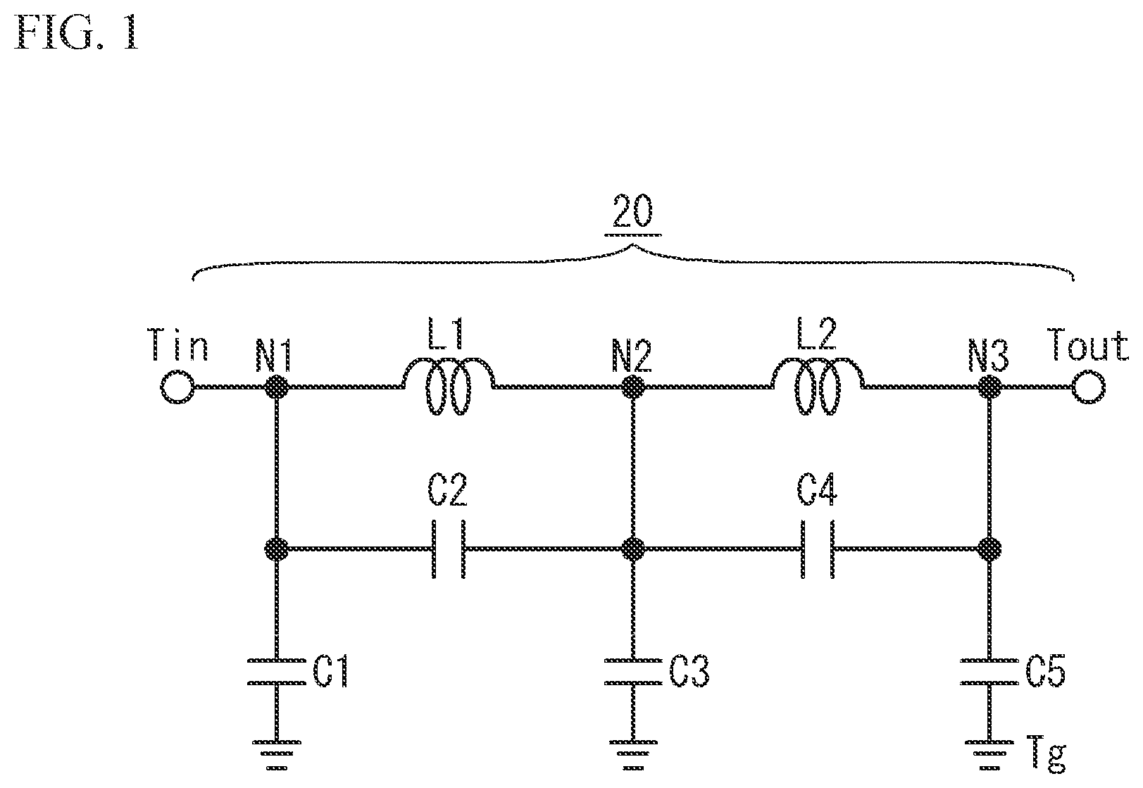
is a circuit diagram of an LPF in a first embodiment;
A and B are a perspective view and a cross-sectional view of a multilayer electronic component in accordance with a first embodiment, respectively;
A to F are plan views illustrating respective dielectric layers in a multilayer structure of the multilayer electronic component in accordance with the first embodiment;
A to D are plan views illustrating respective dielectric layers in the multilayer structure of the multilayer electronic component in accordance with the first embodiment:
A and B are schematic cross-sectional views of a multilayer electronic component in accordance with a first comparative example:
A and B are schematic cross-sectional views of the multilayer electronic component in accordance with the first embodiment;
A to C are plan views illustrating respective dielectric layers in a multilayer structure of a multilayer electronic component in accordance with a first variation of the first embodiment:
A to C are plan views illustrating respective dielectric lavers in a multilayer structure of a multilayer electronic component in accordance with a second variation of the first embodiment:
A to F are plan views illustrating respective dielectric layers in a multilayer structure of a multilayer electronic component in accordance with a third variation of the first embodiment:
A to D are plan views illustrating respective dielectric layers in a multilayer structure of a multilayer electronic component in accordance with a third variation of the first embodiment;
A to C are plan views illustrating respective dielectric layers in a multilayer structure of a multilayer electronic component in accordance with a fourth variation of the first embodiment;
is a perspective view of a simulated structure:
A is a side view of the vicinity of a via wiring line 15 b , and B is a plan view of the vicinity of the via wiring line 15 b;
A to C are graphs presenting the Q factor of an inductor with respect to D 1 to D 3 in the simulation;
A to F are plan views illustrating respective dielectric layers in a multilayer structure of a multilayer electronic component in accordance with a fifth variation of the first embodiment;
A to D are plan views illustrating respective dielectric layers in a multilayer structure of a multilayer electronic component in accordance with the fifth variation of the first embodiment;
A to C are plan views illustrating respective dielectric layers in a multilayer structure of a multilayer electronic component in accordance with a sixth variation of the first embodiment;
A to C are plan views illustrating respective dielectric layers in a multilayer structure of a multilayer electronic component in accordance with a seventh variation of the first embodiment; and
is a circuit diagram of a front-end circuit in which a communication module in accordance with a second embodiment is used.
DETAILED DESCRIPTION
Hereinafter, embodiments of the present disclosure will be described with reference to the accompanying drawings.
First Embodiment
As a first embodiment, a multilayer electronic component having a low-pass filter (LPF) will be described as an example. is a circuit diagram of an LPF in accordance with the first embodiment. As illustrated in , an LPF 20 is connected between an input terminal Tin and an output terminal Tout. The LPF 20 transmits signals in the passband lower than the cutoff frequency to the output terminal Tout among high-frequency signals input to the input terminal Tin, and suppresses signals in frequency bands higher than the cutoff frequency. The LPF 20 includes inductors L 1 and L 2 and capacitors C 1 to C 5 .
The inductors L 1 and L 2 are connected in series between the input terminal Tin and the output terminal Tout. Nodes N 1 to N 3 are provided in a path between the input terminal Tin and the output terminal Tout. The capacitor C 1 is shunt-connected to the node N 1 between the input terminal Tin and the inductor L 1 . The capacitor C 3 is shunt-connected to the node N 2 between the inductors L 1 and L 2 . The capacitor C 5 is shunt-connected to the node N 3 between the inductor L 2 and the output terminal Tout. First ends of the capacitors C 1 , C 3 , and C 5 are coupled to the nodes N 1 to N 3 , respectively, and second ends of the capacitors C 1 , C 3 , and C 5 are coupled to ground terminals Tg. The capacitor C 2 is connected in parallel to the inductor L 1 between the nodes N 1 and N 2 . The capacitor C 4 is connected in parallel to the inductor L 2 between the nodes N 2 and N 3 . In the LPF 20 , the input terminal Tin and the output terminal Tout are electrically connected to each other (i.e., connected in a direct-current (DC) manner).
Table 1 presents examples of the inductances of the inductors L 1 and L 2 and the capacitances of the capacitors C 1 to C 5 .
TABLE 1
L1 L2 C1 C2 C3 C4 C5
5 nH 5 nH 0.7 pF 0.7 pF 1.6 pF 0.7 pF 0.7 pF
The number of inductors and capacitors and the element values (that is, inductance and capacitance) can be set as appropriate.
A and B are a perspective view and a cross-sectional view of the multilayer electronic component in accordance with the first embodiment, respectively. A stack direction of a multilayer structure 10 is defined as a Z direction, a length direction thereof is defined as an X direction, and a width direction thereof is defined as a Y direction. As illustrated in A , the surfaces of both sides in the Z direction of the multilayer structure 10 are an upper surface 10 a (a surface at the +Z side) and a lower surface 10 b (a surface at the −Z side). In a multilayer electronic component 100 , the surfaces of both sides in the Y direction of the multilayer structure 10 are a side surface 10 c (a surface at the +Y side) and a side surface 10 d (a surface at the −Y side). External electrodes 14 are provided on the side surfaces 10 c and 10 d . The external electrode 14 is an electrode for electrically connecting to an external circuit or an external device. The external electrode 14 is bonded to an electrode of the external circuit or the external device by a conductive bonding member such as solder. The external electrodes 14 serve as the input terminal Tin, the output terminal Tout, and the ground terminal Tg. Each external electrode 14 includes an upper-surface electrode 14 a provided on the upper surface 10 a , a lower-surface electrode 14 b provided on the lower surface 10 b , and a side-surface electrode 14 c provided on the side surface 10 c or 10 d . Each external electrode 14 may not necessarily include the upper-surface electrode 14 a and the lower-surface electrode 14 b , and may include only the side-surface electrodes 14 c . By providing the side-surface electrodes 14 c , when the multilayer electronic component 100 is mounted on a mounting substrate, it is possible to observe from above the bonding state between the external electrodes 14 and the mounting substrate by a bonding material such as solder.
As illustrated in B , the multilayer structure 10 includes a plurality of dielectric layers 11 a to 11 i stacked in the Z direction. Conductor patterns 12 a to 12 i are provided on the upper surfaces of the dielectric layers 11 a to 11 i , respectively. In B , conductor patterns 12 b , 12 g , and 12 h are illustrated. Via wiring lines 13 b to 13 h penetrating through the dielectric layers 11 b to 11 h , respectively, are provided. Each of via wiring lines 15 a and 15 b includes the via wiring lines 13 b to 13 h connected in the Z direction. The section including the dielectric layers 11 a to 11 d is an inductor formation section 18 a in which the inductors L 1 and L 2 are formed. The section including the dielectric layers 11 e to 11 i is a capacitor formation section 18 b in which the capacitors C 1 to C 5 are formed. When the multilayer electronic component 100 is mounted on a mounting substrate, if the inductors L 1 and L 2 are close to the mounting substrate, eddy-current loss occurs in the inductors L 1 and L 2 because of the conductor patterns in the mounting substrate, and the Q factors decrease. Therefore, the inductor formation section 18 a is provided at the upper surface 10 a side of the multilayer structure 10 , and the capacitor formation section 18 b is provided between the inductor formation section 18 a and the lower surface 10 b of the multilayer structure 10 . This structure increases the distance between the inductor L 1 and the mounting substrate and the distance between the inductor L 2 and the mounting substrate, and reduces a decrease in the Q factors of the inductors L 1 and L 2 .
A to D are plan views illustrating respective dielectric layers in the multilayer structure of the multilayer electronic component in accordance with the first embodiment. A to C are plan views of the dielectric layers 11 a to 11 i , respectively. D is a plan view of the lower surface of the dielectric layer 11 i as seen through from above. In C , the via wiring lines 13 h are indicated by broken lines. B corresponds to a cross section taken along line A-A in A to D .
As illustrated in A , the conductor pattern 12 a including a direction identification mark and the upper-surface electrodes 14 a are provided on the upper surface 10 a of the dielectric layer 11 a . As illustrated in B , the conductor pattern 12 b including patterns L 1 a and L 2 a is provided on the upper surface of the dielectric layer 11 b . First ends of the patterns L 1 a and L 2 a are coupled to the via wiring lines 13 b that are to be part of the via wiring lines 15 a and 15 b.
As illustrated in C , the conductor pattern 12 c including patterns L 1 b and L 2 b is provided on the upper surface of the dielectric layer 11 c . As illustrated in D , the conductor pattern 12 d including patterns L 1 c and L 2 c is provided on the upper surface of the dielectric layer 11 d . The patterns L 1 a to L 1 c are electrically connected by the via wiring lines 13 b and 13 c to form the inductor L 1 . The patterns L 2 a to L 2 c are electrically connected by the via wiring lines 13 b and 13 c to form the inductor L 2 .
As illustrated in E , the conductor pattern 12 e including patterns C 2 a and C 4 a is provided on the upper surface of the dielectric layer 11 e . As illustrated in F , the conductor pattern 12 f including patterns C 2 b and C 4 b is provided on the upper surface of the dielectric layer 11 f . The patterns C 2 a and C 2 b sandwiching the dielectric layer 11 e therebetween form the capacitor C 2 . The patterns C 4 a and C 4 b sandwiching the dielectric layer 11 e therebetween form the capacitor C 4 .
As illustrated in A , the conductor pattern 12 g including patterns C 1 a , C 3 a , and C 5 a is provided on the upper surface of the dielectric layer 11 g . As illustrated in B , the conductor pattern 12 h including a pattern G is provided on the upper surface of the dielectric layer 11 h . On the upper surface of the dielectric layer 11 h , the pattern G is coupled to the side-surface electrodes 14 c that form the ground terminals Tg. The pattern G includes patterns C 1 b , C 3 b , and C 5 b . The patterns C 1 a and C 1 b sandwiching the dielectric layer 11 g therebetween form the capacitor C 1 . The patterns C 3 a and C 3 b sandwiching the dielectric layer 11 g therebetween form the capacitor C 3 . The patterns C 5 a and C 5 b sandwiching the dielectric layer 11 g therebetween form the capacitor C 5 .
As illustrated in C , the conductor pattern 12 i including patterns 16 a and 16 b is provided on the upper surface of the dielectric layer 11 i . On the upper surface of the dielectric layer 11 i , the pattern 16 a is connected to the side-surface electrode 14 c that forms the input terminal Tin. Thus, the pattern 16 a electrically connects the via wiring line 15 a and the input terminal Tin. On the upper surface of the dielectric layer 11 i , the pattern 16 b is connected to the side-surface electrode 14 c forming the output terminal Tout. As a result, the pattern 16 b electrically connects the via wiring line 15 b and the output terminal Tout. As illustrated in D , the lower-surface electrodes 14 b are provided on the lower surface 10 b of the dielectric layer 11 i . As described above, a first end of the pattern L 1 a provided on the upper surface of the dielectric layer 11 b is electrically connected to the input terminal Tin through the via wiring line 15 a and the pattern 16 a . A first end of the pattern L 2 a provided on the upper surface of the dielectric layer 11 b is electrically connected to the output terminal Tout through the via wiring line 15 b and the pattern 16 b.
The dielectric layers 11 a to 11 i are made of a ceramic material and contain, for example, an oxide of silicon, calcium, and magnesium (for example, CaMgSi 2 O 6 , which is a diopside crystal) as a main component. The main components of the dielectric layers 11 a to 11 i may be oxides other than oxides of Si, Ca, and/or Mg. Furthermore, the dielectric layers 11 a to 11 i may contain an oxide of at least one of the following elements: Ti, Zr, and Al as an insulating material.
The conductor patterns 12 a to 12 i , the via wiring lines 13 b to 13 i , and the external electrodes 14 are non-magnetic metal layers containing, for example, Ag, Pd, Pt, Cu, Ni, Au, Au—Pd alloy, or Ag—Pt alloy as a main component. The external electrode 14 may contain a non-conductive material such as TiO 2 , ZrO 2 , or Al 2 O 3 in addition to the above metal material.
The multilayer structure 10 is manufactured as follows, for example. The dielectric layers 11 a to 11 i are formed using, for example, a doctor-blade method. The via wiring lines 13 b to 13 i penetrating through the dielectric layers 11 b to 11 i are formed. For example, via holes penetrating through the dielectric layers 11 a to 11 i are formed by laser light irradiation. The via wiring lines 13 b to 13 i are formed in the via holes using a squeegee method or the like. The conductor patterns 12 a to 12 i are formed on the surfaces of the dielectric layers 11 a to 11 i . The conductor patterns 12 a to 12 i are formed using, for example, a screen printing method or a transfer method. The dielectric layers 11 a to 11 i are stacked to form the multilayer structure 10 . For example, thermal pressurization or an adhesive is used to stack the dielectric layers 11 a to 11 i . The multilayer structure 10 is fired at, for example, 700° C. or higher. As a result, the dielectric layers 11 a to 11 i become a sintered body. The side-surface electrodes 14 c are formed on the side surfaces of the multilayer structure 10 .
A and B are schematic cross-sectional views of a multilayer electronic component in accordance with a first comparative example. As illustrated in A , in the first comparative example, the inductors L 1 and L 2 are formed by the conductor pattern 12 b in the inductor formation section 18 a . A first end of the inductor L 1 is coupled to the input terminal Tin in the inductor formation section 18 a , and a first end of the inductor L 2 is coupled to the output terminal Tout in the inductor formation section 18 a . The capacitor C is formed by patterns Ca and Cb sandwiching the dielectric layer 11 e therebetween in the capacitor formation section 18 b . The pattern Ca is electrically connected to a second end of the inductor L 1 and a second end of the inductor L 2 through the via wiring lines 13 b to 13 d . The pattern Cb is electrically connected to the ground pattern G through the via wiring lines 13 f to 13 g . As a result, the inductors L 1 and L 2 are connected in series between the input terminal Tin and the output terminal Tout, and the capacitor C is shunt-connected.
As illustrated in B , when the multilayer structure 10 is formed, the positions of the dielectric layers 11 a to 11 i may shift. For example, the dielectric layer 11 g is shifted in the +X direction. As a result, as indicated by a broken line 50 , the positions of the via wiring lines 13 f and 13 g are shifted, and the via wiring lines 13 f and 13 g are disconnected. Or, the contact resistance between the via wiring lines 13 f and 13 g is increased. However, even when the electric continuity between the input terminal Tin and the output terminal Tout is inspected, it is impossible to inspect the positional deviation of the dielectric layers 11 c to 11 i below the inductor formation section 18 a . Further, the continuity check between the input terminal Tin or the output terminal Tout and the ground terminal Tg cannot be performed because of the capacitor C.
A and B are schematic cross-sectional views of the multilayer electronic component in accordance with the first embodiment. As illustrated in A , in the first embodiment, a first end of the inductor L 1 is electrically connected to the input terminal Tin through the via wiring line 15 a and the pattern 16 a , and a first end of the inductor L 2 is electrically connected to the output terminal Tout through the via wiring line 15 b and the pattern 16 b . As described above, the inductors L 1 and L 2 are not connected to the input terminal Tin or the output terminal Tout in the inductor formation section 18 a . The inductors L 1 and L 2 are electrically connected to the input terminal Tin and the output terminal Tout through the patterns 16 a and 16 b that are located lower than the capacitor formation section 18 b.
As illustrated in B , when the dielectric layer 11 g is shifted in the +X direction, as indicated by broken lines 50 a and 50 b , the via wiring lines 13 g forming the via wiring lines 15 a and 15 b are shifted in the +X direction. When the electric continuity between the input terminal Tin and the output terminal Tout is inspected, detected is disconnection or high resistance between the input terminal Tin and the output terminal Tout. Therefore, it is possible to inspect positional deviation of the dielectric layers 11 b to 11 h in the inductor formation section 18 a and the capacitor formation section 18 b . Further, defects in the via wiring lines 13 b to 13 h can be inspected. As the continuity check, the electric continuity between the input terminal Tin and the output terminal Tout may be checked using a direct current or an alternating current.
First Variation of the First Embodiment
A to C are plan views illustrating dielectric layers in a multilayer structure of a multilayer electronic component in accordance with a first variation of the first embodiment. The dielectric layers 11 a to 11 g are the same as those in A to A of the first embodiment. A and B are plan views of the dielectric layers 11 h and 11 i , respectively. C is a plan view of the lower surface of the dielectric layer 11 i as seen through from above. In C , the via wiring lines 13 i are indicated by broken lines.
As illustrated in A , the configurations of the conductor pattern 12 h on the dielectric layer 11 h and the via wiring lines 13 h are the same as those in B . As illustrated in B , the conductor pattern 12 i is not provided on the dielectric layer 11 i . The via wiring lines 13 i penetrating through the dielectric layer 11 i are provided. Each of the via wiring lines 15 a and 15 b is formed of the via wiring lines 13 b to 13 i that are connected.
As illustrated in C , the lower-surface electrodes 14 b provided on the lower surface 10 b of the dielectric layer 11 i include patterns 17 a and 17 b . The via wiring line 15 a is electrically connected to the input terminal Tin through the pattern 17 a . The via wiring line 15 b is electrically connected to the output terminal Tout through the pattern 17 b . Other configurations are the same as those in the first embodiment, and a description thereof will be omitted. In the first variation of the first embodiment, the continuity check of the dielectric layer 11 i can be performed in addition to the dielectric layers 11 b to 11 h.
Second Variation of the First Embodiment
A to C are plan views illustrating respective dielectric layers in a multilayer structure of a multilayer electronic component in accordance with a second variation of the first embodiment. The dielectric layers 11 a to 11 g are the same as those in A to A of the first embodiment. A and B are plan views illustrating the dielectric layers 11 h and 11 i , respectively. C is a plan view of the lower surface of the dielectric layer 11 i as seen through from above. In C , the via wiring lines 13 i are indicated by broken lines.
As illustrated in A , the configurations of the conductor pattern 12 h on the dielectric layer 11 h and the via wiring lines 13 h are the same as those in B . As illustrated in B , the conductor pattern 12 i including the patterns 16 a and 16 b is provided on the dielectric layer 11 i . The via wiring lines 15 a and 15 b are coupled to the patterns 16 a and 16 b , respectively. The patterns 16 a and 16 b are coupled to the input terminal Tin and the output terminal Tout, respectively.
As illustrated in C , the via wiring lines 15 a and 15 b are coupled to the patterns 17 a and 17 b , respectively. The patterns 17 a and 17 b are coupled to the input terminal Tin and the output terminal Tout, respectively. Other configurations are the same as those in the first embodiment, and a description thereof will be omitted. In the second variation of the first embodiment, the patterns 16 a and 17 a are connected in parallel between the via wiring line 15 a and the input terminal Tin, and the patterns 16 b and 17 b are connected in parallel between the via wiring line 15 b and the output terminal Tout. Thus, the parasitic inductance between the via wiring line 15 a and the input terminal Tin can be reduced, and the parasitic inductance between the via wiring line 15 b and the output terminal Tout can be reduced.
Third Variation of the First Embodiment
A to D are plan views illustrating respective dielectric layers in a multilayer structure of a multilayer electronic component in accordance with a third variation of the first embodiment. A to D are plan views of the dielectric layers 11 a to 11 i , respectively. D is a plan view of the lower surface of the dielectric layer 11 i as seen through from above. In D , the via wiring lines 13 i are indicated by broken lines.
As illustrated in A , the dielectric layer 11 a is the same as that illustrated in A of the first embodiment. As illustrated in B , the via wiring line 15 a is not provided, and a first end of the pattern L 1 a is coupled to the input terminal Tin. C to E are the same as C and E of the first embodiment, respectively, except that the via wiring line 15 a is not provided. As illustrated in F , the via wiring line 15 a is not provided, and the pattern C 2 b is coupled to the input terminal Tin on the upper surface of the dielectric layer 11 f . As illustrated in A , the via wiring line 15 a is not provided, and the pattern C 1 a is coupled to the input terminal Tin on the upper surface of the dielectric layer 11 g . B and C are the same as B and C of the first variation of the first embodiment, respectively, except that the via wiring line 15 a is not provided. As illustrated in D , the via wiring line 15 b is coupled to the pattern 17 b , and the pattern 17 b is coupled to the output terminal Tout. Other configurations are the same as those in the first variation of the first embodiment, and a description thereof will be omitted. As in the third variation of the first embodiment, one of the via wiring lines 15 a and 15 b may be omitted.
Fourth Variation of the First Embodiment
A to C are plan views illustrating respective dielectric layers in a multilayer structure of a multilayer electronic component in accordance with a fourth variation of the first embodiment. A to C are plan views of the dielectric layers 11 d to 11 f , respectively. The dielectric layers 11 a to 11 c and 11 g to 11 i are the same as those in the first embodiment or the first variation of the first embodiment.
As illustrated in A , the width W 3 a of a via wiring line 13 d 1 electrically connected between the patterns L 1 c and L 2 c is larger than the widths W 3 of the via wiring lines 13 d in the via wirings 15 a and 15 b . As illustrated in B , the width W 3 a of a via wiring 13 el provided between the patterns C 2 a and C 4 a is larger than the widths W 3 of the via wiring lines 13 e in the via wiring lines 15 a and 15 b . As illustrated in C , the width W 3 a of a via wiring line 13 f 1 coupled to the via wiring line 13 el is larger than the widths W 3 of the via wiring lines 13 f in the via wiring lines 15 a and 15 b . Other configurations are the same as those in the first embodiment or the first variation of the first embodiment, and a description thereof will be omitted.
It is possible to detect misalignment of the dielectric layers 11 b to 11 i by inspecting the electric continuity between the input terminal Tin and the output terminal Tout. In addition, it is possible to inspect the electric continuity failure of the via wiring lines 15 a and 15 b due to a cause other than misalignment. However, it is difficult to inspect the electric continuity failure due to a cause other than misalignment in the via wiring lines 13 d 1 to 13 f 1 other than the via wiring lines 15 a and 15 b . Therefore, the widths W 3 a of the via wiring lines 13 d 1 to 13 f 1 other than the via wiring lines 15 a and 15 b are adjusted to be larger than the widths W 3 of the via wiring lines 15 a and 15 b . This configuration causes the via wiring lines 13 d 1 to 13 f 1 to be less likely to be disconnected or to be less likely to have high resistance. Therefore, even when it is not possible to inspect the electric continuity failure due to a cause other than misalignment in the via wiring lines 13 d 1 to 13 f 1 , it is possible to inhibit the via wiring lines 13 d 1 to 13 f 1 from being defective.
In the first embodiment and the first to fourth variations thereof, the side-surface electrode 14 c (a second side-surface electrode) corresponding to the input terminal Tin and the side-surface electrode 14 c (a first side-surface electrode) corresponding to the output terminal Tout are provided on the side surface 10 c of the multilayer structure 10 . The inductors L 1 and L 2 are provided in the multilayer structure 10 . The capacitors C 1 to C 5 are provided between the inductors L 1 and L 2 and the lower surface 10 b (a first surface). The via wiring line 15 b penetrates through the dielectric layers 11 b to 11 h (or 11 i ) between the dielectric layers 11 b and 11 h (or 11 i ), and electrically connects a first end of the inductor L 2 and the output terminal Tout. Here, the dielectric layer 11 b (a first dielectric layer) is in contact with the inductors L 1 and L 2 . The dielectric layer 11 h (or 11 i ) (a second dielectric layer) is located closer to the lower surface 10 b than at least a part of each of the capacitors C 1 to C 5 . The input terminal Tin and the output terminal Tout are electrically connected to each other through the inductor L 2 and the via wiring lines 15 b . Thus, as illustrated in B , by inspecting the electric continuity between the input terminal Tin and the output terminal Tout, it is possible to inspect defects in the dielectric layers 11 b to 11 h.
The inductor L 2 is not electrically connected to the terminal Tout at the positions closer to the upper surface 10 a (a second surface) than the positions of the capacitors C 1 to C 5 . Thus, by inspecting the electric continuity between the input terminal Tin and the output terminal Tout, it is possible to inspect defects of the dielectric layers 11 b to 11 h.
As in the first embodiment and the first variation thereof, another via wiring line 15 a penetrates through the dielectric layers 11 b to 11 h (or 11 b to 11 i ) and electrically connects a second end of the inductor L 1 to the input terminal Tin. This structure allows defects of the dielectric layers 11 b to 11 h to be inspected accurately because the electric continuity in the via wiring lines 15 a and 15 b can be inspected, as compared with the case in which the via wiring line 15 a is not provided as in the second variation of the first embodiment.
As illustrated in A to C of the fourth variation of the first embodiment, the planar areas of the via wiring lines 13 d 1 to 13 f 1 penetrating through the dielectric layer 11 d to 11 f (at least one dielectric layer of the dielectric layers 11 a to 11 i ) other than the via wiring lines 15 a and 15 b electrically connected between the input terminal Tin and the output terminal Tout are larger than the planar areas of the via wiring lines 15 a and 15 b . This configuration inhibits defects of the via wiring lines 13 d 1 to 13 f of which the electric continuity failure due to a cause other than misalignment of the dielectric layers 11 b to 11 h cannot be inspected. The planar areas of the via wiring lines 13 d 1 to 13 f 1 are preferably equal to or greater than 1.5 times, more preferably equal to or greater than 2 times the planar areas of the via wiring lines 15 a and 15 b.
As illustrated in C of the first embodiment, the pattern 16 b , which is provided between the adjacent dielectric layers 11 h and 11 i between at least a part of each of the capacitors C 1 to C 5 and the lower surface 10 b and electrically connects the via wiring line 15 b and the output terminal Tout, is provided. This structure allows the via wiring line 15 b and the output terminal Tout to be electrically connected. The lower-surface electrodes 14 b may be omitted as in the first variation of the first embodiment.
As illustrated in C of the first variation of the first embodiment, the lower-surface electrodes 14 b are provided on the lower surface 10 b and are connected to the respective side-surface electrodes 14 c . The via wiring 15 b is connected to the pattern 17 b of the lower-surface electrode 14 b . This structure allows the via wiring line 15 b to be electrically connected to the output terminal Tout.
First ends of the capacitors C 1 , C 3 , and C 5 are connected to a path between the input terminal Tin and the output terminal Tout, and second ends of the capacitors C 1 , C 3 , and C 5 are connected to the ground terminals Tg (ground electrodes) provided on the surface of the multilayer structure 10 . By shunt-connecting the capacitors C 1 , C 3 , and C 5 , the LPF 20 including the inductors L 1 and L 2 and the capacitors C 1 to C 5 can be formed.
The first embodiment and the variations thereof have described a case in which the first side-surface electrode and the second side-surface electrode are the output terminal Tout and the input terminal Tin as an example, but the side-surface electrode may be a terminal other than the output terminal Tout and the input terminal Tin. Although an example in which the first side-surface electrode and the second side-surface electrode are provided on the same side surface 10 c has been described, the first side-surface electrode may be provided on the side surface 10 c , and the second side-surface electrode may be provided on the side surface 10 d . The cutoff frequency of the LPF 20 is, for example, 0.5 GHz to 5 GHz. Although an example in which the multilayer electronic component includes the LPF 20 has been described, the multilayer electronic component may be other than a low pass filter. Further, the multilayer electronic component may include a filter other than the low-pass filter.
Simulation
The Q factor of the inductor was simulated by electromagnetic field analysis. is a perspective view of the simulated structure. A is a side view of the vicinity of the via wiring line 15 b , and B is a plan view of the vicinity of the via wiring line 15 b . As illustrated in to B , an inductor L 1 composed of patterns La and Lb is provided in the multilayer structure 10 . The external electrode 14 is provided from the upper surface 10 a to the lower surface 10 b through the side surface 10 c of the multilayer structure 10 . The external electrode 14 includes the upper-surface electrode 14 a provided on the upper surface 10 a , the lower-surface electrode 14 b provided on the lower surface 10 b , and the side-surface electrode 14 c provided on the side surface 10 c . A first end of the inductor L is electrically connected to the lower-surface electrode 14 b through the via wiring line 15 b . A second end of the inductor L is connected to the via wiring line 15 a.
The simulation conditions are as follows.
Multilayer Structure 10
•
• Width Wx 1 : 2.5 mm • Width Wy 1 : 2.0 mm • Thickness T 1 : 0.6 mm • Relative permittivity: 10 Inductor L • Internal diameter Wx 2 : 700 μm • Internal diameter Wy 2 : 600 μm • Width W 2 : 60 μm • Thickness T 2 : 10 μm Frequency at which Q factors were simulated: 3.3 GHz Width W 1 of the external electrode 14 : 40 μm Width of the via wiring line 15 b: 50 μm
The center of the side-surface electrode 14 c in the X direction and the center of the via wiring line 15 b in the X direction substantially coincide with each other. The distance between the side surface 10 c and the via wiring line 15 b is represented by D 1 , the width of the upper-surface electrode 14 a in the Y direction is represented by D 2 , and the distance between the upper surface 10 a and the inductor L is represented by D 3 .
A to C are graphs presenting the Q factor of the inductor with respect to D 1 to D 3 in the simulation. Dots are simulated values. The straight line in A is an approximate straight line of the dots. In A , the Q factor of the inductor L was simulated while D 2 was fixed to 0 mm (that is, no upper-surface electrode 14 a is provided), D 3 was fixed to 0.035 mm, and D 1 was varied. A sample A is a sample in which the side-surface electrode 14 c is provided on the side surface 10 c , and a sample B is a sample in which the side-surface electrode 14 c is not provided on the side surface 10 c and the lower-surface electrode 14 b is provided only on the lower surface 10 b . In the sample B, as D 1 becomes shorter, the Q factor improves. This is because when D 1 is shortened, the distance between the via wiring line 15 b and the spirally winding portion of the inductor L becomes longer. In the sample A, in the range where D 1 is 0.05 mm or greater, the Q factor improves as D 1 becomes shorter. This is the same as the sample B. In the range where D 1 is 0.05 mm or less, the Q factor decreases as D 1 becomes shorter. This is considered because the via wiring line 15 b becomes closer to the side-surface electrode 14 c . Thus, the distance D 1 between the via wiring line 15 b and the side-surface electrode 14 c is preferably 50 μm or greater. In consideration of manufacturing errors, D 1 is more preferably 75 μm or greater, and further preferably 100 μm or greater.
In B , the Q factor of the inductor L was simulated while D 1 was fixed to 0.1 mm, D 3 was fixed to 0.035 mm. D 2 was varied. In the range where D 2 is 0.1 mm or less, the Q factor is almost constant. In the range where D 2 is 0.1 mm or greater, the Q factor decreases, and the variation in the Q factor increases. In the range D 2 is 0.1 mm or greater, the upper-surface electrode 14 a overlaps the inductor L and the via wiring line 15 b in a plan view. This is considered the reason why the Q factor decreased. It is preferable that the upper-surface electrode 14 a do not overlap the inductor L or the via wiring line 15 b in a plan view.
In C , the Q factor of the inductor L was simulated while D 1 was fixed to 0.1 mm, D 2 was fixed to 0.2 mm, and D 3 was varied. In the range where D 3 is 0.05 mm or greater, the Q factor is almost constant. In the range where D 3 is 0.05 mm or less, the Q factor decreases as D 3 becomes shorter. This is because the inductor L becomes closer to the upper-surface electrode 14 a.
As described above, it is preferable that the upper-surface electrode 14 a do not overlap the inductor L or the via wiring line 15 b in a plan view. In the case that the upper-surface electrode 14 a overlaps the inductor L and the via wiring line 15 b , the distance D 3 between the inductor L and the upper-surface electrode 14 a is preferably adjusted to be 50 μm or greater. In consideration of manufacturing errors, D 3 is more preferably 75 μm or greater, and further preferably 100 μm or greater.
Fifth Variation of the First Embodiment
A to D are plan views illustrating respective dielectric layers in a multilayer structure of a multilayer electronic component in accordance with a fifth variation of the first embodiment. A to C are plan views of the dielectric layers 11 a to 11 i , respectively. D is a plan view of the lower surface of the dielectric layer 11 i as seen through from above. In D , the via wiring lines 13 i are indicated by broken lines.
As illustrated in A , the dielectric layer 11 a is the same as that illustrated in A of the first embodiment. As illustrated in B , the via wiring line 15 a is provided between the input terminal Tin and the ground terminal Tg in the X direction, and the via wiring line 15 b is provided between the output terminal Tout and the ground terminal Tg in the X direction. Other configurations are the same as those in B . In C to B , the shapes of the conductor patterns 12 c to 12 h are different from those in C to B according to the positions of the via wiring lines 15 a and 15 b . As illustrated in C , the positions of the via wiring lines 15 a and 15 b are different from those in B . As illustrated in D , the pattern 17 a extends to the +X side more than the input terminal Tin and is coupled to the via wiring line 15 a . The pattern 17 b extends to the −X side more than the output terminal Tout and is coupled to the via wiring line 15 b . Other configurations are the same as those in the first variation of the first embodiment, and a description thereof will be omitted.
As in the simulation, the longer distances D 3 between the via wiring lines 15 a and 15 b and the input terminal Tin and the output terminal Tout improve the Q factor of the inductor. However, as D 3 increases, the size of the multilayer electronic component increases. Therefore, in the fifth variation of the first embodiment, the via wiring lines 15 a and 15 b do not overlap the input terminal Tin or the output terminal Tout as viewed in the Y direction (the thickness direction of the side-surface electrode). This configuration allows the distance D 4 between the via wiring line 15 a and the input terminal Tin and the distance D 4 between the via wiring line 15 b and the output terminal Tout to be, for example, 50 μm or greater even when the distance D 3 between each of the via wiring lines 15 a and 15 b and the side surface 10 c is short, as illustrated in C . Therefore, it is possible to reduce the size of the multilayer electronic component and to improve the Q factors of the inductors L 1 and L 2 . As the via wiring lines 15 a and 15 b are closer to the ground terminals Tg, the Q factor decreases because of eddy-current loss. The decrease in the Q factor caused by the via wiring lines 15 a and 15 b close to the ground terminals Tg is larger than the decrease in the Q factor caused by the via wiring lines 15 a and 15 b close to the input terminal Tin and the output terminal Tout. Therefore, the distance D 4 is preferably shorter than the distances D 5 between the ground terminals Tg and the via wiring lines 15 a and 15 b . The distance D 4 is preferably equal to or less than ½ of the distance D 5 .
Sixth Variation of the First Embodiment
A to C are plan views illustrating respective dielectric layers in a multilayer structure of a multilayer electronic component in accordance with a sixth variation of the first embodiment. The dielectric layers 11 a to 11 g are the same as those in A to A of the fifth variation of the first embodiment. A and B are plan views of the dielectric layers 11 h and 11 i , respectively. C is a plan view of the lower surface of the dielectric layer 11 i as seen through from above. In B , the via wiring lines 13 h are indicated by broken lines.
As illustrated in A , the configurations of the conductor pattern 12 h on the dielectric layer 11 h and the via wiring lines 13 h are the same as those in B . As illustrated in B , the conductor pattern 12 i including the patterns 16 a and 16 b is provided on the dielectric layer 11 i . The pattern 16 a extends to the +X side more than the input terminal Tin and is coupled to the via wiring line 15 a . The pattern 16 b extends to the −X side more than the output terminal Tout and is coupled to the via wiring line 15 b . As illustrated in C , the via wiring line 13 i penetrating through the dielectric layer 11 i is not provided. Other configurations are the same as those of the fifth variation of the first embodiment, and a description thereof will be omitted. As in the sixth variation of the first embodiment, the via wiring lines 15 a and 15 b may be not necessarily provided in the dielectric layer 11 i.
Seventh Variation of the First Embodiment
A to C are plan views illustrating respective dielectric layers in a multilayer structure of a multilayer electronic component in accordance with to a seventh variation of the first embodiment. The dielectric layers 11 a to 11 g are the same as those in A to A of the fifth variation of the first embodiment. A and B are plan views of the dielectric layers 11 h and 11 i , respectively. C is a plan view of the lower surface of the dielectric layer 11 i as seen through from above. In B and C , the via wiring line 13 h and the via wiring line 13 i are indicated by broken lines.
As illustrated in A , the configurations of the conductor pattern 12 h on the dielectric layer 11 h and the via wiring lines 13 h are the same as those in B . As illustrated in B , as viewed from the Y direction, the via wiring lines 13 h are provided so as not to overlap the input terminal Tin or the output terminal Tout, and the via wiring lines 13 i are provided so as to overlap the input terminal Tin and the output terminal Tout, respectively. The patterns 16 a and 16 b are not coupled to the input terminal Tin or the output terminal Tout, and electrically connect the via wiring lines 13 h and 13 i . As illustrated in C , the configurations of the lower-surface electrodes 14 b and the via wiring lines 13 i are the same as those in C of the first variation of the first embodiment. Other configurations are the same as those in the sixth variation of the first embodiment, and a description thereof will be omitted. As in the seventh variation of the first embodiment, in the via wiring lines 15 a (and 15 b ), the via wiring lines 13 h and 13 i may have different planar positions, and the patterns 16 a (and 16 b ) may electrically connect the via wiring lines 13 h and 13 i . As in the seventh variation of the first embodiment, it is only required that at least a part of each of the via wiring lines 15 a and 15 b does not overlap with the input terminal Tin or the output terminal Tout as viewed from the Y direction. This configuration can reduce the size of the multilayer electronic component and improve the Q factors of the inductors L 1 and L 2 .
Second Embodiment
A second embodiment is an example of a multiplexer and a communication module in which the first embodiment and the variations thereof are used. is a circuit diagram of a front-end circuit in which the communication module according to the second embodiment is used. As illustrated in , the front-end circuit includes a triplexer 30 , switches 34 , duplexers 37 , power amplifiers (PA) 38 , and low-noise amplifiers (LNA) 39 . The triplexer 30 includes a high-pass filter (HPF) 31 , a band-pass filter (BPF) 32 , and a low-pass filter (LPF) 33 .
An antenna 40 is connected to a common terminal Ta. First ends of the HPF 31 , the BPF 32 , and the LPF 33 are commonly coupled to the common terminal Ta. The switches 34 are coupled to second ends of the HPF 31 , the BPF 32 , and the LPF 33 , respectively. The HPF 31 allows high-frequency signals in the high band to pass therethrough and suppresses signals with other frequencies. The BPF 32 allows high-frequency signals in the middle band, which is lower in frequency than the high band, to pass therethrough, and suppresses signals with other frequencies. The LPF 33 allows high-frequency signals in the low band, which is lower in frequency than the middle band, to pass therethrough, and suppresses signals with other frequencies.
Common nodes Na of the duplexers 37 are coupled to the switch 34 . Each switch 34 selects one of the duplexers 37 and connects it to the corresponding one of the second ends of the HPF 31 , the BPF 32 , and the LPF 33 . The duplexer 37 includes a transmit filter 35 that is a BPF and a receive filter 36 that is a BPF. The transmit filter 35 and the receive filter 36 are coupled to the PA 38 and the LNA 39 , respectively.
The transmission signals input to a transmission terminal Tx are amplified by the PA 38 . The transmit filter 35 outputs high-frequency signals in the transmit band among the amplified signals to the common node Na and suppresses signals with other frequencies. The filtered transmit signal passes through the switch 34 and either the HPF 31 , the BPF 32 or the LPF 33 and is output from the antenna 40 .
The reception signal input to the antenna 40 passes through either the HPF 31 , the BPF 32 , or the LPF 33 and the switch 34 . The receive filter 36 allows signals in the receive band among high-frequency signals input to the common node Na to pass therethrough and suppresses signals with other frequencies. The filtered reception signal is amplified by the LNA 39 and output to the receive terminal Rx.
The filter according to any one of the first embodiment and the variations thereof can be used for the LPF 33 of the triplexer 30 . The multilayer electronic component may include, in addition to the LPF 33 , at least one of the BPF 32 or the HPF 31 . Although the triplexer 30 has been described as an example of the multiplexer, the multiplexer may be a diplexer, a duplexer, or a quadplexer.
Although the embodiments of the present invention have been described in detail, the present invention is not limited to such a specific embodiment, and it is to be understood that the various change, substitutions, and alterations could be made hereto without departing from the spirit and scope of the invention.
Figures (19)
Citations
This patent cites (11)
- US5945892
- US2015/0028969
- US2019/0333691
- US203734631
- US118487571
- USH 09-238040
- US2009-159328
- US2013-150100
- US5598548
- US2017-212717
- USWO 2018/142667