Pixel Circuit and Drive Method Therefor, Display Panel and Display Device
Abstract
Provided are a pixel circuit and a drive method therefor, a display panel and a display device. The pixel circuit includes: a light emitting device; a drive transistor configured to generate, according to a data voltage, a drive current for driving the light emitting device to emit light; a data writing circuit coupled to the drive transistor, where the data writing circuit is configured to input the data voltage in response to a signal applied to the data writing circuit; and a voltage control circuit coupled to the drive transistor, where the voltage control circuit is configured to reset a control electrode, a first electrode and a second electrode of the drive transistor in response to a signal applied to the voltage control circuit before the data voltage is input.
Claims (13)
1 . A pixel circuit, comprising: a light emitting device; a drive transistor configured to generate, according to a data voltage, a drive current for driving the light emitting device to emit light; a data writing circuit coupled to the drive transistor; and a voltage control circuit comprising a first transistor, a second transistor and a storage capacitor; wherein a control electrode of the first transistor is coupled to a first control signal terminal, a first electrode of the first transistor is coupled to a first initialization signal terminal, and a second electrode of the first transistor is coupled to a control electrode of the drive transistor; a control electrode of the second transistor is coupled to a second control signal terminal, a first electrode of the second transistor is coupled to the control electrode of the drive transistor, and a second electrode of the second transistor is coupled to a second electrode of the drive transistor; and a first electrode of the storage capacitor is coupled to the control electrode of the drive transistor, and a second electrode of the storage capacitor is coupled to a first electrode of the drive transistor; wherein the voltage control circuit is configured to, before the data voltage is input, reset the control electrode, the first electrode and the second electrode of the drive transistor in response to a signal applied to the voltage control circuit; wherein the data writing circuit comprises a fifth transistor and a sixth transistor; a control electrode of the fifth transistor is coupled to a fifth control signal terminal, a first electrode of the fifth transistor is coupled to the first electrode of the drive transistor and a second electrode of the fifth transistor is directly connected to a first electrode of the sixth transistor; and a control electrode of the sixth transistor is coupled to a sixth control signal terminal, and a second electrode of the sixth transistor is coupled to a data signal terminal; wherein the data writing circuit is further configured to: in response to a fifth control signal applied to the fifth control signal terminal and a sixth control signal applied to the sixth control signal terminal, input the data voltage applied to a data signal terminal to the first electrode of the drive transistor; wherein the data writing circuit is further configured to: in response to the fifth control signal applied to the fifth control signal terminal and the sixth control signal applied to the sixth control signal terminal, input the data voltage applied to the data signal terminal to the first electrode of the drive transistor; wherein the second control signal, the fifth control signal, and the sixth control signal are different signals with different timing diagrams, a kickoff moment of an active level of the fifth control signal is earlier than a kickoff moment of an active level of the second control signal and the kickoff moment of the active level of the second control signal is earlier than a kickoff moment of the active level of the sixth control signal, a duration of the active level of the second control signal, a duration of the active level of the fifth control signal and a duration of the active level of the sixth control signal have overlapping time, and the overlapping time is smaller than a duration of an active level of the first control signal and the duration of the active level of the second control signal respectively; wherein the active level of each first, second, fifth and sixth control signal is a level of control signal that, when applied to the control electrode, turns on corresponding first, second, fifth, and sixth transistor; wherein the pixel circuit further comprises a threshold compensation circuit; and the threshold compensation circuit is coupled to the drive transistor; and the threshold compensation circuit is configured to: while the data voltage is input, compensate a threshold voltage of the drive transistor in response to a third control signal applied to a third control signal terminal; wherein the threshold compensation circuit comprises: a third transistor; wherein a control electrode of the third transistor is coupled to the third control signal terminal, a first electrode of the third transistor is directly connected to the control electrode of the drive transistor, and a second electrode of the third transistor is directly coupled to the second electrode of the drive transistor.
Show 12 dependent claims
2 . The pixel circuit according to claim 1 , wherein the voltage control circuit is further configured to: while the data voltage is input, compensate the threshold voltage of the drive transistor in response to the second control signal applied to the second control signal terminal.
3 . The pixel circuit according to claim 1 , wherein the data writing circuit is further configured to: in response to a fourth control signal applied to a fourth control signal terminal, input the data voltage applied to the data signal terminal to the first electrode of the drive transistor.
4 . The pixel circuit according to claim 3 , wherein the data writing circuit comprises a fourth transistor; wherein a control electrode of the fourth transistor is coupled to the fourth control signal terminal, a first electrode of the fourth transistor is coupled to the data signal terminal, and a second electrode of the fourth transistor is coupled to the first electrode of the drive transistor.
5 . The pixel circuit according to claim 4 , wherein a duration of an active level of the fourth control signal is not longer than a duration of the active level of the first control signal.
6 . The pixel circuit according to claim 1 , wherein at least one of the duration of the active level of of the fifth control signal and the duration of the active level of the sixth control signal is substantially the same as the duration of the active level of the second control signal.
7 . The pixel circuit according to claim 1 , wherein the fifth control signal terminal and the second control signal terminal are a same signal terminal.
8 . The pixel circuit according to claim 1 , wherein the pixel circuit further comprises: an element reset circuit coupled to the light emitting device; wherein the element reset circuit is configured to: in response to a seventh control signal of a seventh control signal terminal, provide a second initialization signal of a second initialization signal terminal to the light emitting device.
9 . The pixel circuit according to claim 8 , wherein the seventh control signal terminal and one of the first control signal terminal to the fourth control signal terminal are a same signal terminal.
10 . A display panel, comprising: a plurality of sub-pixels, wherein at least one of the plurality of sub-pixels comprises the pixel circuit of claim 1 ; a plurality of control signal lines, wherein at least one of the plurality of control signal lines is coupled to the pixel circuit in a row of sub-pixels; and a drive and control circuit, wherein the drive and control circuit is coupled to the plurality of control signal lines.
11 . The display panel according to claim 10 , wherein the plurality of control signal lines comprise a plurality of first control signal lines, a plurality of second control signal lines, a plurality of fifth control signal lines and a plurality of sixth control signal lines; wherein one of the first control signal lines is coupled to a first control signal terminal of a pixel circuit in a row of sub-pixels; one of the second control signal lines is coupled to a second control signal terminal of a pixel circuit in the row of sub-pixels; one of the fifth control signal lines is coupled to a fifth control signal terminal of a pixel circuit in the row of sub-pixels; and one of the sixth control signal lines is coupled to a sixth control signal terminal of a pixel circuit in the row of sub-pixels; the drive and control circuit comprises a first driving control circuit, and the first driving control circuit comprises a plurality of first driving shift register units sequentially arranged; a plurality of first driving shift register units adjacent to each other serve as a first unit group, and one row of sub-pixels correspond to one first unit group; and in the first unit group; a first one of the plurality of first driving shift register units is coupled to a first control signal line coupled to a corresponding row of sub-pixels; a third one of the plurality of first driving shift register units is coupled to a fifth control signal line coupled to the corresponding row of sub-pixels; a fourth one of the plurality of first driving shift register units is coupled to a second control signal line coupled to the corresponding row of sub-pixels; and a fifth one of the plurality of first driving shift register units is coupled to a sixth control signal line coupled to the corresponding row of sub-pixels.
12 . The display panel according to claim 10 , wherein the plurality of control signal lines comprise a plurality of first control signal lines, a plurality of second control signal lines and a plurality of sixth control signal lines; one of the first control signal lines is coupled to a first control signal terminal of a pixel circuit in a row of sub-pixels; one of the second control signal lines is coupled to a second control signal terminal and a fifth control signal terminal of the pixel circuit in a row of sub-pixels; and one of the sixth control signal lines is coupled to a sixth control signal terminal of a pixel circuit in the row of sub-pixels; the drive and control circuit comprises a second driving control circuit, and the second driving control circuit comprises a plurality of second driving shift register units sequentially arranged; a plurality of second driving shift register units adjacent to each other serve as a second unit group, and one row of sub-pixels correspond to one second unit group; and in the second unit group: a first one of the plurality of second driving shift register units is coupled to a first control signal line coupled to a corresponding row of sub-pixels; a third one of the plurality of second driving shift register units is coupled to a second control signal line coupled to the corresponding row of sub-pixels; and a fifth one of the plurality of second driving shift register units is coupled to a sixth control signal line coupled to the corresponding row of sub-pixels.
13 . The display panel according to claim 10 , wherein the plurality of control signal lines comprise plurality of first control signal lines, a plurality of second control signal lines and a plurality of fourth control signal lines; one of the first control signal lines is coupled to a first control signal terminal of a pixel circuit in a row of sub-pixels; one of the second control signal lines is coupled to a second control signal terminal of a pixel circuit in the row of sub-pixels; and one of the fourth control signal lines is coupled to a fourth control signal terminal of a pixel circuit in a row of sub-pixels; the drive and control circuit comprises a third driving control circuit and a fourth driving control circuit; the third driving control circuit comprises a plurality of third driving shift register units sequentially arranged; a plurality of third driving shift register units adjacent to each other serve as a third unit group, and one row of sub-pixels correspond to one third unit group; in the third unit group: a first one of the plurality of third driving shift register units is coupled to a first control signal line coupled to a corresponding row of sub-pixels; and a fifth one of the plurality of third driving shift register units is coupled to a second control signal line coupled to a corresponding row of sub-pixels; the fourth driving control circuit comprises a plurality of fourth driving shift register units sequentially arranged; one row of sub-pixels correspond to one fourth driving shift register unit; and the fourth driving shift register unit is coupled to a fourth control signal line coupled to a corresponding row of sub-pixels.
Full Description
Show full text →
CROSS REFERENCE TO RELATED APPLICATIONS
This application is a national phase entry under 35 U.S.C. § 371 of International Application No. PCT/CN2022/088832, filed on Apr. 24, 2022, the entire content of which is incorporated herein by reference.
FIELD
The disclosure relates to the field of display technology, and particularly to a pixel circuit and a drive method therefor, a display panel and a display device.
BACKGROUND
With advantages of self-illumination and low energy consumption, electroluminescent diodes such as an organic light emitting diode (OLED), a quantum dot light emitting diode (QLED) and a micro light emitting diode (Micro LED) have become a focus of application and research of electroluminescent display devices at present. Generally, pixel circuits are used in the electroluminescent display devices to drive the electroluminescent diodes to emit light.
SUMMARY
An embodiment of the disclosure provides a pixel circuit. The pixel circuit includes: a light emitting device, a drive transistor configured to generate, according to a data voltage, a drive current for driving the light emitting device to emit light, a data writing circuit coupled to the drive transistor, the data writing circuit being configured to input the data voltage by a data writing circuit in response to a signal applied to the data writing circuit, and a voltage control circuit coupled to the drive transistor, where the voltage control circuit is configured to reset a control electrode, a first electrode and a second electrode of the drive transistor in response to a signal applied to the voltage control circuit, before the data voltage is input.
In some examples, the voltage control circuit is further configured to: in response to a first control signal applied to a first control signal terminal, provide a first initialization signal applied to a first initialization signal terminal to the control electrode of the drive transistor, so as to reset the control electrode of the drive transistor; and in response to a second control signal applied to a second control signal terminal, reset the first electrode and the second electrode of the drive transistor.
In some examples, the voltage control circuit includes a first transistor, a second transistor and a storage capacitor. A control electrode of the first transistor is coupled to the first control signal terminal, a first electrode of the first transistor is coupled to the first initialization signal terminal, and a second electrode of the first transistor is coupled to the control electrode of the drive transistor. A control electrode of the second transistor is coupled to the second control signal terminal, a first electrode of the second transistor is coupled to the control electrode of the drive transistor, and a second electrode of the second transistor is coupled to the second electrode of the drive transistor. A first electrode of the storage capacitor is coupled to the control electrode of the drive transistor, and a second electrode of the storage capacitor is coupled to the first electrode of the drive transistor.
In some examples, the voltage control circuit is further configured to, while the data voltage is input, compensate a threshold voltage of the drive transistor in response to the second control signal applied to the second control signal terminal.
In some examples, the pixel circuit further includes a threshold compensation circuit. The threshold compensation circuit is coupled to the drive transistor, and the threshold compensation circuit is configured to: while the data voltage is input, compensate the threshold voltage of the drive transistor in response to a third control signal applied to a third control signal terminal.
In some examples, the threshold compensation circuit includes a third transistor. A control electrode of the third transistor is coupled to the third control signal terminal, a first electrode of the third transistor is coupled to the control electrode of the drive transistor, and a second electrode of the third transistor is coupled to the second electrode of the drive transistor.
In some examples, the data writing circuit is further configured to: in response to a fourth control signal applied to a fourth control signal terminal, input the data voltage applied to a data signal terminal to the first electrode of the drive transistor.
In some examples, the data writing circuit includes a fourth transistor. A control electrode of the fourth transistor is coupled to the fourth control signal terminal, a first electrode of the fourth transistor is coupled to the data signal terminal, and a second electrode of the fourth transistor is coupled to the first electrode of the drive transistor.
In some examples, a duration of an active level of the fourth control signal is not longer than a duration of an active level of the first control signal.
In some examples, the data writing circuit is further configured to: in response to a fifth control signal applied to a fifth control signal terminal and a sixth control signal applied to a sixth control signal terminal, input the data voltage applied to a data signal terminal to the first electrode of the drive transistor. An active level of the fifth control signal and an active level of the sixth control signal have second overlapping time. A kickoff moment of the active level of the fifth control signal is earlier than a kickoff moment of the active level of the sixth control signal.
In some examples, the data writing circuit includes a fifth transistor and a sixth transistor. A control electrode of the fifth transistor is coupled to the fifth control signal terminal, a first electrode of the fifth transistor is coupled to the first electrode of the drive transistor, and a second electrode of the fifth transistor is coupled to a first electrode of the sixth transistor. A control electrode of the sixth transistor is coupled to the sixth control signal terminal, and a second electrode of the sixth transistor is coupled to the data signal terminal.
In some examples, a duration of an active level of at least one of the fifth control signal and the sixth control signal is substantially the same as a duration an active level of the second control signal.
In some examples, the kickoff moment of the active level of the fifth control signal is earlier than a kickoff moment of the active level of the second control signal, and the kickoff moment of the active level of the second control signal is earlier than the kickoff moment of the active level of the sixth control signal.
In some examples, the fifth control signal terminal and the second control signal terminal are the same signal terminal.
In some examples, the pixel circuit further includes an element reset circuit coupled to the light emitting device. The element reset circuit is configured to: in response to a seventh control signal of a seventh control signal terminal, provide a second initialization signal of a second initialization signal terminal to the light emitting device.
In some examples, the seventh control signal terminal and one of the first control signal terminal to the fourth control signal terminal are the same signal terminal.
An embodiment of the disclosure provides a display panel. The display panel includes the above pixel circuit.
In some examples, the display panel includes: a plurality of sub-pixels, where at least one of the plurality of sub-pixels includes the above pixel circuit; a plurality of control signal lines, where at least one of the plurality of control signal lines is coupled to the pixel circuit in a row of sub-pixels; and a drive and control circuit, where the drive and control circuit is coupled to the plurality of control signal lines.
In some examples, the plurality of control signal lines include a plurality of first control signal lines, a plurality of second control signal lines, a plurality of fifth control signal lines and a plurality of sixth control signal lines. One of the first control signal lines is coupled to a first control signal terminal of a pixel circuit in a row of sub-pixels, one of the second control signal lines is coupled to a second control signal terminal of the pixel circuit in a row of sub-pixels, one of the fifth control signal lines is coupled to a fifth control signal terminal of a pixel circuit in the row of sub-pixels, and one of the sixth control signal lines is coupled to a sixth control signal terminal of a pixel circuit in the row of sub-pixels. The drive and control circuit includes a first driving control circuit. The first driving control circuit includes a plurality of first driving shift register units sequentially arranged, a plurality of first driving shift register units adjacent to each other serve as a first unit group, and one row of sub-pixels correspond to one first unit group. In the first unit group, a first one of first driving shift register units is coupled to a first control signal line coupled to a corresponding row of sub-pixels, a third one of first driving shift register units is coupled to a fifth control signal line coupled to the corresponding row of sub-pixels, a fourth one of first driving shift register units is coupled to a second control signal line coupled to the corresponding row of sub-pixels, and a fifth one of first driving shift register units is coupled to a sixth control signal line coupled to the corresponding row of sub-pixels.
In some examples, the plurality of control signal lines include a plurality of first control signal lines, a plurality of second control signal lines and a plurality of sixth control signal lines. One of the first control signal lines is coupled to a first control signal terminal of a pixel circuit in a row of sub-pixels, one of the second control signal lines is coupled to a second control signal terminal and a fifth control signal terminal of a pixel circuit in the row of sub-pixels, and one of the sixth control signal lines is coupled to a sixth control signal terminal of a pixel circuit in a row of sub-pixels. The drive and control circuit includes a second driving control circuit. The second driving control circuit includes a plurality of second driving shift register units sequentially arranged; a plurality of second driving shift register units adjacent to each other serve as a second unit group, and one row of sub-pixels correspond to one second unit group. In the second unit group, a first one of second driving shift register units is coupled to a first control signal line coupled to a corresponding row of sub-pixels, a third one of second driving shift register units is coupled to a second control signal line coupled to the corresponding row of sub-pixels, and a fifth one of second driving shift register units is coupled to a sixth control signal line coupled to the corresponding row of sub-pixels.
In some examples, the plurality of control signal lines include a plurality of first control signal lines, a plurality of second control signal lines and a plurality of fourth control signal lines. One of the first control signal lines is coupled to a first control signal terminal of a pixel circuit in a row of sub-pixels, one of the second control signal lines is coupled to a second control signal terminal of a pixel circuit in a row of sub-pixels, and one of the fourth control signal lines is coupled to a fourth control signal terminal of a pixel circuit in a row of sub-pixels. The drive and control circuit includes a third driving control circuit and a fourth driving control circuit. The third driving control circuit includes a plurality of third driving shift register units sequentially arranged; a plurality of third driving shift register units adjacent to each other serve as a third unit group, and a row of sub-pixels correspond to one third unit group. In the third unit group, a first one of third driving shift register units is coupled to a first control signal line coupled to a corresponding row of sub-pixels, and a fifth one third driving shift register units is coupled to a second control signal line coupled to a corresponding row of sub-pixels. The fourth driving control circuit includes a plurality of fourth driving shift register units sequentially arranged; a row of sub-pixels correspond to one fourth driving shift register unit; and the fourth driving shift register unit is coupled to a fourth control signal line coupled to a corresponding row of sub-pixels.
An embodiment of the disclosure provides a display device. The display device includes the above display panel.
An embodiment of the disclosure provides a drive method for the above pixel circuit. The drive method includes: in a reset stage, resetting a control electrode, a first electrode and a second electrode of a drive transistor by a voltage control circuit, in response to a signal applied to the voltage control circuit before a data voltage is input; in a data writing stage, inputting the data voltage by a data writing circuit in response to a signal applied to the data writing circuit; and in a light emission stage, generating, by the drive transistor according to the data voltage, a drive current for driving a light emitting device to emit light, so as to drive the light emitting device to emit light.
BRIEF DESCRIPTION OF THE DRAWINGS
shows a schematic structural diagram of a pixel circuit according to an embodiment of the disclosure.
shows a schematic structural diagram of another pixel circuit according to an embodiment of the disclosure.
shows a specific schematic structural diagram of a pixel circuit according to an embodiment of the disclosure.
A shows a timing chart of signals according to an embodiment of the disclosure.
B shows a timing chart of signals according to an embodiment of the disclosure.
shows a flow chart of a drive method for a pixel circuit according to an embodiment of the disclosure.
shows a specific schematic structural diagram of a pixel circuit according to an embodiment of the disclosure.
shows a timing chart of signals according to an embodiment of the disclosure.
shows a timing chart of signals according to an embodiment of the disclosure.
shows a timing chart of signals according to an embodiment of the disclosure.
shows a specific schematic structural diagram of a pixel circuit according to an embodiment of the disclosure.
shows a timing chart of signals according to an embodiment of the disclosure.
shows a specific schematic structural diagram of a pixel circuit according to an embodiment of the disclosure.
A shows a timing chart of signals according to an embodiment of the disclosure.
B shows a timing chart of signals according to an embodiment of the disclosure.
shows a specific schematic structural diagram of a pixel circuit according to an embodiment of the disclosure.
shows a timing chart of signals according to an embodiment of the disclosure.
shows a specific schematic structural diagram of a pixel circuit according to an embodiment of the disclosure.
shows a timing chart of signals according to an embodiment of the disclosure.
shows a schematic structural diagram of a display panel according to an embodiment of the disclosure.
shows a schematic structural diagram of a display panel according to an embodiment of the disclosure.
shows a schematic structural diagram of a display panel according to an embodiment of the disclosure.
shows a schematic structural diagram of a display panel according to an embodiment of the disclosure.
shows a schematic structural diagram of a display panel according to an embodiment of the disclosure.
DETAILED DESCRIPTION
In order to make objectives, technical solutions and advantages of embodiments of the disclosure clearer, the technical solutions of the disclosure will be clearly and completely described below in combination with accompanying drawings in the embodiments of the disclosure. Apparently, the described embodiments are merely some embodiments rather than all embodiments of the disclosure. In addition, embodiments of the disclosure and features in the embodiments can be combined with each other without conflict. On the basis of the described embodiments of the disclosure, all other embodiments obtained by those of ordinary skill in the art without making creative efforts fall within the scope of protection of the disclosure.
Unless otherwise defined, technical terms or scientific terms used in the disclosure should have the ordinary meanings understood by those of ordinary skill in the art to which the disclosure belongs. “First”, “second” and other similar words used in the disclosure do not indicate any order, quantity or importance, but are merely used to distinguish between different components. “Comprise”, “include” or other similar words mean that an element or object appearing before the word contains elements or objects listed after the word and equivalents thereof, without excluding other elements or objects. “Connected”, “connected with each other” or other similar words are not limited to physical or mechanical connections, but can include electrical connections, whether direct or indirect.
It should be noted that sizes and shapes of all figures in accompanying drawings do not reflect true scales and are merely intended to illustrate contents of the disclosure. In addition, throughout the description, identical or similar reference numerals denote identical or similar elements or elements having identical or similar functions.
It should be noted that in an actual process, due to a limitation of process conditions or other factors, the same as mentioned in the disclosure cannot be completely the same, and there may be some measurement errors. Therefore, a fluctuation within 20% of the same relation in embodiments of the disclosure is allowable, which all fall within the scope of protection of the disclosure.
In some embodiments of the disclosure, a display device may include a display panel. The display panel may include a substrate. Herein, the substrate may include a display region and a non-display region (that is, a region of the substrate other than the display region). The display region may include a plurality of pixel units arranged in an array. In some embodiments, each pixel unit includes sub-pixels in the same color or sub-pixels in a plurality of different colors. For example, the pixel units may include red sub-pixels, green sub-pixels and blue sub-pixels, and color display may be implemented by mixing red, green and blue. Alternatively, the pixel units may include red sub-pixels, green sub-pixels, blue sub-pixels and white sub-pixels, and color display may be implemented by mixing red, green, blue and white. During practical application, illumination colors of the sub-pixels in the pixel units may be designed and determined according to practical application scenarios, and are not limited herein. The pixel units including red sub-pixels, green sub-pixels and blue sub-pixels are taken as an example for description below.
In some embodiments of the disclosure, each sub-pixel may include a pixel circuit, and the pixel circuit may include a drive transistor M 0 and a light emitting device L, so as to control the light emitting device L to emit light, thereby enabling the display panel to implement a image display function. However, a threshold voltage Vth of the drive transistor M 0 may shift due to a process, aging and other reasons, which may affect a generated drive current. Moreover, a hysteresis effect during switching between a high gray scale and a low gray scale may cause a ghosting.
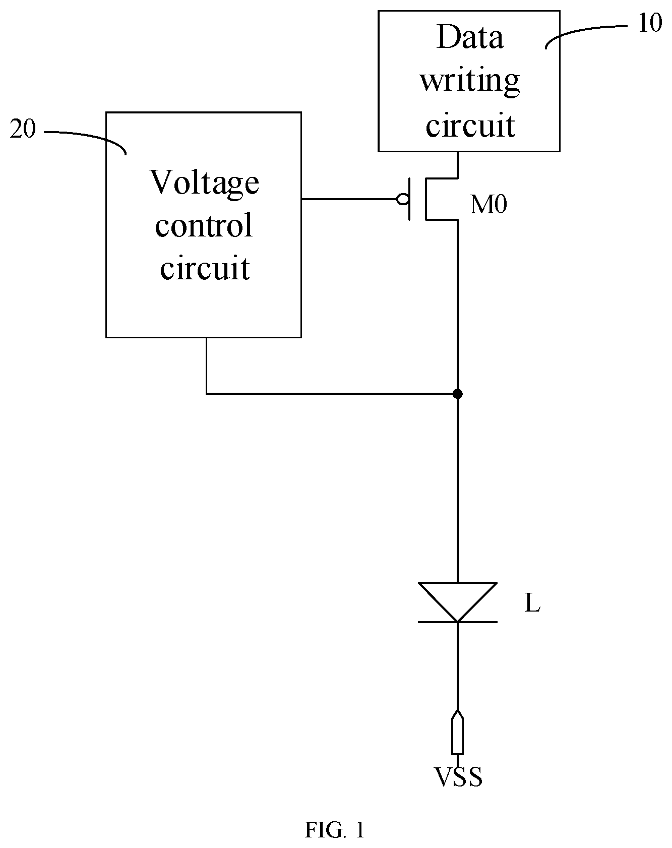
In order to solve the above problems, an embodiment of the disclosure provides some pixel circuits. As shown in , the pixel circuit may include: a drive transistor M 0 , a data writing circuit 10 and a light emitting device L. The data writing circuit 10 is coupled to the drive transistor M 0 , and a voltage control circuit 20 is coupled to the drive transistor M 0 . In addition, the drive transistor M 0 may be configured to generate, according to a data voltage, a current for driving the light emitting device L to emit light. The data writing circuit 10 may be configured to provide the data voltage in response to an applied signal. Moreover, the voltage control circuit 20 may be configured to reset a control electrode, a first electrode and a second electrode of the drive transistor M 0 in response to the loaded signal before the data voltage is input.
According to the pixel circuit provided in an embodiment of the disclosure, by arranging the voltage control circuit, the control electrode, the first electrode and the second electrode of the drive transistor may be reset before the data voltage is input. In this way, while the pixel circuit works in each display frame, before the data voltage is input, a voltage of the control electrode of the drive transistor is substantially the same, a voltage of the first electrode of the drive transistor is substantially the same, and a voltage of the second electrode of the drive transistor is substantially the same, thereby solving the ghosting problem caused by a hysteresis effect during switching between a high gray scale and a low gray scale.
In some embodiments of the disclosure, as shown in , the voltage control circuit 20 may be coupled to a first control signal terminal CS 1 , a first initialization signal terminal VINIT 1 , a second control signal terminal CS 2 , and the control electrode and the second electrode of the drive transistor M 0 . In addition, the voltage control circuit 20 is further configured to, in response to a first control signal cs 1 applied to the first control signal terminal CS 1 , provide a first initialization signal applied to the first initialization signal terminal VINIT 1 to the control electrode of the drive transistor M 0 , so as to reset the control electrode of the drive transistor M 0 , and is configured to reset the first electrode and the second electrode of the drive transistor M 0 in response to a second control signal cs 2 applied to the second control signal terminal CS 2 . Further, the voltage control circuit 20 is further configured to compensate, while the data voltage is input, a threshold voltage of the drive transistor M 0 in response to the second control signal cs 2 applied to the second control signal terminal CS 2 .
In some embodiments of the disclosure, as shown in , the data writing circuit 10 may be coupled to a fourth control signal terminal CS 4 , a data signal terminal DA and the first electrode of the drive transistor M 0 . In addition, the data writing circuit 10 may be configured to provide, in response to a fourth control signal cs 4 applied to the fourth control signal terminal CS 4 , the data voltage applied to the data signal terminal DA to the first electrode of the drive transistor M 0 .
In some embodiments of the disclosure, as shown in , the pixel circuit may further include a light emission control circuit 30 . The light emission control circuit 30 may be coupled to the drive transistor M 0 and the light emitting device L. In addition, the light emission control circuit 30 may be configured to, in response to a first light emission control signal em 1 from a first light emission control signal terminal EM 1 , cause the first electrode of the drive transistor M 0 to be coupled to a first power supply terminal; and cause the second electrode of the drive transistor M 0 to be coupled to the light emitting device L in response to a second light emission control signal em 2 from a second light emission control signal terminal EM 2 . In some embodiments, the light emission control circuit 30 may be coupled to the first power supply terminal, the first electrode and the second electrode of the drive transistor M 0 , and a first electrode of the light emitting device L.
In some embodiments of the disclosure, as shown in , the pixel circuit may further include an element reset circuit 40 . The element reset circuit 40 is coupled to the light emitting device L. In addition, the element reset circuit 40 is configured to provide a second initialization signal from a second initialization signal terminal VINIT 2 to the light emitting device L in response to a seventh control signal cs 7 from a seventh control signal terminal CS 7 . In some embodiments, the element reset circuit 40 may be coupled to the seventh control signal terminal CS 7 , the second initialization signal terminal VINIT 2 , and the first electrode of the light emitting device L.
In some embodiments of the disclosure, the first electrode of the light emitting device L may be coupled to the second electrode of the drive transistor M 0 , or the first electrode of the light emitting device L may be coupled to the second electrode of the drive transistor M 0 via the light emission control circuit 30 . The second electrode of the light emitting device L may be coupled to a second power supply terminal VSS. In addition, the first electrode of the light emitting device L may be an anode thereof, and the second electrode may be a cathode thereof. In some embodiments, the light emitting device L may be an electroluminescent diode. For example, the light emitting device L may include at least one of a micro light emitting diode (Micro LED), an organic light emitting diode (OLED), and a quantum dot light emitting diode (QLED). During practical application, the specific structure of the light emitting device L may be designed and determined according to practical application scenarios, and is not limited herein.
In some embodiments of the disclosure, as shown in , the drive transistor M 0 may be a P-type transistor. The first electrode of the drive transistor M 0 may be a source, the second electrode of the drive transistor M 0 may be a drain. When the drive transistor M 0 is in a saturation state, a current flows from the source to the drain of the drive transistor M 0 . Alternatively, the drive transistor M 0 may be an N-type transistor, which is not limited herein.
In some embodiments of the disclosure, as shown in , the voltage control circuit 20 may include: a first transistor M 1 , a second transistor M 2 and a storage capacitor CST. A control electrode of the first transistor M 1 is coupled to the first control signal terminal CS 1 , a first electrode of the first transistor M 1 is coupled to the first initialization signal terminal VINIT 1 , and a second electrode of the first transistor M 1 is coupled to the control electrode of the drive transistor M 0 . Moreover, a control electrode of the second transistor M 2 is coupled to the second control signal terminal CS 2 , a first electrode of the second transistor M 2 is coupled to the control electrode of the drive transistor M 0 , and a second electrode of the second transistor M 2 is coupled to the second electrode of the drive transistor M 0 . Moreover, a first electrode of the storage capacitor CST is coupled to the control electrode of the drive transistor M 0 , and a second electrode of the storage capacitor CST is coupled to the first electrode of the drive transistor M 0 .
In some embodiments, the first transistor M 1 may be turned on under the control of an active level of the first control signal cs 1 , and may be turned off under the control of an inactive level of the first control signal cs 1 . For example, the first transistor M 1 is a P-type transistor, an active level of the first control signal cs 1 is a low level, and an inactive level of the first control signal cs 1 is a high level. Alternatively, the first transistor M 1 is an N-type transistor, an active level of the first control signal cs 1 is a high level, and an inactive level of the first control signal cs 1 is a low level.
In some embodiments, the second transistor M 2 may be turned on under the control of an active level of the second control signal cs 2 , and may be turned off under the control of an inactive level of the second control signal cs 2 . For example, the second transistor M 2 is a P-type transistor, an active level of the second control signal cs 2 is a low level, and an inactive level of the second control signal cs 2 is a high level. Alternatively, the second transistor M 2 is an N-type transistor, an active level of the second control signal cs 2 is a high level, and an inactive level of the second control signal cs 2 is a low level.
In some embodiments of the disclosure, as shown in , the data writing circuit 10 may include a fourth transistor M 4 . A control electrode of the fourth transistor M 4 is coupled to a fourth control signal terminal CS 4 , a first electrode of the fourth transistor M 4 is coupled to a data signal terminal DA, and a second electrode of the fourth transistor M 4 is coupled to the first electrode of the drive transistor M 0 . In some embodiments, the fourth transistor M 4 may be turned on under the control of an active level of the fourth control signal cs 4 , and may be turned off under the control of an inactive level of the fourth control signal cs 4 . For example, the fourth transistor M 4 is a P-type transistor, an active level of the fourth control signal cs 4 is a low level, and an inactive level of the fourth control signal cs 4 is a high level. Alternatively, the fourth transistor M 4 is an N-type transistor, an active level of the fourth control signal cs 4 is a high level, and an inactive level of the fourth control signal cs 4 is a low level.
It should be noted that in an embodiment of the disclosure, preferably, one transistor may be arranged in the data writing circuit 10 . In this way, less transistors are included in the pixel circuit, and an occupied space thereof in the display panel is small.
In some embodiments of the disclosure, as shown in , the light emission control circuit 30 may include a seventh transistor M 7 and an eighth transistor M 8 . A control electrode of the seventh transistor M 7 is coupled to the first light emission control signal terminal EM 1 , a first electrode of the seventh transistor M 7 is coupled to the first power supply terminal, and a second electrode of the seventh transistor M 7 is coupled to the first electrode of the drive transistor M 0 . Moreover, a control electrode of the eighth transistor M 8 is coupled to the second light emission control signal terminal EM 2 , a first electrode of the eighth transistor M 8 is coupled to the second electrode of the drive transistor M 0 , and a second electrode of the eighth transistor M 8 is coupled to the light emitting device L.
In some embodiments, the seventh transistor M 7 may be turned on under the control of an active level of the first light emission control signal em 1 , and may be turned off under the control of an inactive level of the first light emission control signal em 1 . For example, the seventh transistor M 7 is a P-type transistor, an active level of the first light emission control signal em 1 is a low level, and an inactive level of the first light emission control signal em 1 is a high level. Alternatively, the seventh transistor M 7 is an N-type transistor, an active level of the first light emission control signal em 1 is a high level, and an inactive level of the first light emission control signal em 1 is a low level.
In some embodiments, the eighth transistor M 8 may be turned on under the control of an active level of the second light emission control signal em 2 , and may be turned off under the control of an inactive level of the second light emission control signal em 2 . For example, under the condition that the eighth transistor M 8 is a P-type transistor, an active level of the second light emission control signal em 2 is a low level, and an inactive level of the second light emission control signal em 2 is a high level. Alternatively, under the condition that the eighth transistor M 8 is an N-type transistor, an active level of the second light emission control signal em 2 is a high level, and an inactive level of the second light emission control signal em 2 is a low level.
In some embodiments of the disclosure, as shown in , the element reset circuit 40 may include a ninth transistor M 9 . A control electrode of the ninth transistor M 9 is coupled to the seventh control signal terminal CS 7 , a first electrode of the ninth transistor M 9 is coupled to the second initialization signal terminal VINIT 2 , and a second electrode of the ninth transistor M 9 is coupled to the light emitting device L. In some embodiments, the ninth transistor M 9 may be turned on under the control of an active level of the seventh light emission control signal, and may be turned off under the control of an inactive level of the seventh light emission control signal. For example, the ninth transistor M 9 is a P-type transistor, an active level of the seventh light emission control signal is a low level, and an inactive level of the seventh light emission control signal is a high level. Alternatively, the ninth transistor M 9 is an N-type transistor, an active level of the seventh light emission control signal is a high level, and an inactive level of the seventh light emission control signal is a low level.
Generally, a transistor having an active layer made of a low temperature poly-silicon (LTPS) material has a high migration rate, may be made thinner and less, and has lower power consumption, etc. During specific implementation, a material of an active layer of at least one of the above transistors may be set as a low temperature poly-silicon material. In this way, the above transistor may be an LTPS type transistor, such that a pixel circuit may have a high migration rate, may be made thinner and less, and has lower power consumption, etc.
Generally, a transistor having an active layer made of a metal oxide semiconductor material has a relatively small leakage current. Therefore, in order to reduce a leakage current, in some embodiments of the disclosure, a material of an active layer of at least one of the above transistors may include a metal oxide semiconductor material, such as indium gallium zinc oxide (IGZO), or other metal oxide semiconductor materials, which is not limited herein. In this way, the above transistor may be an oxide thin film transistor, so as to reduce a leakage current of a pixel circuit.
In some embodiments, all the transistors may be LTPS type transistors. Alternatively, all the transistors may be oxide type transistors. Alternatively, some of the transistors may be oxide type transistors, and the remaining transistors may be LTPS type transistors. For example, the first transistor M 1 and the second transistor M 2 are oxide type transistors, and the remaining transistors are LTPS type transistors. In this way, processes for preparing the LTPS type transistor and the oxide type transistor are combined to prepare a pixel circuit made of a low temperature poly-silicon oxide (LTPS) such that a leakage current of the control electrode of the drive transistor M 0 may be relatively small, and power consumption is relatively low. Therefore, by applying the pixel circuit to a display panel, when a refresh frequency of the display panel is reduced for display, display uniformity may be ensured.
During specific implementation, based on a type of a transistor and a signal of a control electrode thereof, the control electrode of the transistor may serve as a gate, a first electrode of the transistor may serve as a source, and a second electrode of the transistor may serve as a drain; or, a first electrode of the transistor may serve as a drain, and a second electrode of the transistor may serve as s source, which may be designed and determined according to actual application scenario, and is not be specifically distinguished herein.
What are mentioned above are merely examples taken to illustrate the specific structure of each circuit in the pixel circuits provided in an embodiment of the disclosure. During specific implementation, the specific structure of the above circuit is not limited to the above structure provided in an embodiment of the disclosure, and may be other structures known by those skilled in the art, which all fall within the scope of protection of the disclosure, and are not limited herein.
In some embodiments of the disclosure, the first power supply terminal may be configured to provide a constant first power supply voltage, and the first power supply voltage is generally positive. Moreover, the second power supply terminal may be configured to provide a constant second power supply voltage, and the second power supply voltage may generally be a grounding voltage or negative. During practical application, specific values of the first power supply voltage and the second power supply voltage may be designed and determined according to practical application scenarios, and are not limited herein.
What are mentioned above are merely examples taken to illustrate the specific structure of each circuit in the pixel circuits provided in an embodiment of the disclosure. During specific implementation, the specific structure of the above circuit is not limited to the above structure provided in an embodiment of the disclosure, and may be other structures known by those skilled in the art, which all fall within the scope of protection of the disclosure, and are not limited herein.
Each of the above transistors being a P-type transistor is taken as an example for description. In some embodiments, a timing chart of signals corresponding to a pixel circuit shown in is shown in A . A duration tcs 1 of an active level (for example, a high level) of the first control signal cs 1 may be substantially the same as a duration tcs 2 of an active level (for example, a high level) of the second control signal cs 2 . In addition, a kickoff moment kcs 1 of the active level (for example, a high level) of the first control signal cs 1 is earlier than a kickoff moment kcs 2 of the active level of the second control signal cs 2 (for example, a high level).
In some embodiments, as shown in A , the active level (for example, a high level) of the first control signal cs 1 and the active level (for example, a high level) of the second control signal cs 2 may have no overlapping time.
In some embodiments, as shown in A , a kickoff moment kcs 4 of an active level (for example, a high level) of the fourth control signal cs 4 may be later than a kickoff moment kcs 4 of the active level (for example, a high level) of the second control signal cs 2 . In addition, there may be a time gap tg between the kickoff moment kcs 4 and the kickoff moment kcs 2 . In some embodiments, the time gap tg may be shorter than, longer than or equal to a duration of a data writing stage. During practical application, the time gap tg may be determined according to requirements of practical applications, which is not limited herein.
In some embodiments, as shown in A , a duration tcs 4 of the active level (for example, a high level) of the fourth control signal cs 4 may be shorter than a duration tcs 1 of the active level (for example, a high level) of the first control signal cs 1 .
In some embodiments, as shown in A , the fourth control signal cs 4 and the seventh control signal cs 7 may be controlled to have substantially the same timing.
In some embodiments, as shown in A , the first light emission control signal em 1 and the second light emission control signal em 2 may be controlled to have substantially the same timing.
As shown in , a drive method for a pixel circuit provided in an embodiment of the disclosure may include steps as follows.
S 100 : in a reset stage, reset a control electrode, a first electrode and a second electrode of a drive transistor by a voltage control circuit in response to a signal applied to the voltage control circuit before a data voltage is input.
S 200 : in a data writing stage, input a data voltage by a data writing circuit in response to a signal applied to the data writing circuit.
S 300 : in a light emission stage, generate, by the drive transistor according to the data voltage, a drive current for driving a light emitting device to emit light, so as to drive the light emitting device to emit light.
A working process of a pixel circuit provided in an embodiment of the disclosure in one display frame is described below by taking the structure of the pixel circuit shown in as an example and in combination with the signal timing chart shown in A . The reset stage T 1 , the data writing stage T 2 and the light emission stage T 3 in the signal timing chart shown in A are mainly illustrated. The reset stage T 1 includes a stage T 11 and a stage T 12 . Sign em 1 represents the first light emission control signal em 1 applied to the first light emission control signal terminal EM 1 . Sign em 2 represents the second light emission control signal em 2 applied to the second light emission control signal terminal EM 2 . Sign cs 1 represents the first control signal cs 1 applied to the first control signal terminal CS 1 . Sign cs 2 represents the second control signal cs 2 applied to the second control signal terminal CS 2 . Sign cs 4 represents the fourth control signal cs 4 applied to the fourth control signal terminal CS 4 . Sign cs 7 represents the seventh control signal cs 7 applied to the seventh control signal terminal CS 7 .
In the stage T 11 of the reset stage T 1 , the second transistor M 2 is turned off under the control of the high level of the signal cs 2 . The fourth transistor M 4 is turned off under the control of the high level of the signal cs 4 . The seventh transistor M 7 is turned off under the control of the high level of the signal em 1 . The eighth transistor M 8 is turned off under the control of the high level of the signal em 2 . The ninth transistor M 9 is turned off under the control of the high level of the signal cs 7 . The first transistor M 1 is turned on under the control of the low level of the signal cs 1 to provide the first initialization voltage vinit 1 applied to the first initialization signal terminal VINIT 1 to the control electrode of the drive transistor M 0 , so as to reset the control electrode of the drive transistor M 0 , and maintain the voltage of the control electrode of the drive transistor M 0 by the storage capacitor CST.
In the stage T 12 of the reset stage T 1 , the first transistor M 1 is turned off under the control of the high level of the signal cs 1 . The fourth transistor M 4 is turned off under the control of the high level of the signal cs 4 . The seventh transistor M 7 is turned off under the control of the high level of the signal em 1 . The eighth transistor M 8 is turned off under the control of the high level of the signal em 2 . The ninth transistor M 9 is turned off under the control of the high level of the signal cs 7 . The second transistor M 2 is turned on under the control of the low level of the signal cs 2 , so as to cause the control electrode to be coupled to the second electrode of the drive transistor M 0 , such that the drive transistor M 0 works in a diode manner. Since the storage capacitor CST maintains the voltage of the control electrode of the drive transistor M 0 as the first initialization voltage vinit 1 , it is possible to change the voltage of the second electrode of the drive transistor M 0 into the first initialization voltage vinit 1 , and change the voltage of the first electrode of the drive transistor M 0 into vinit 1 -Vth. here Vth represents the threshold voltage of the drive transistor M 0 . In this way, the control electrode, the first electrode and the second electrode of the drive transistor M 0 may be reset before the data voltage is written. In addition, after reset, the voltage of the control electrode of the drive transistor M 0 is the first initialization voltage vinit 1 , the voltage of the second electrode changes into the first initialization voltage vinit 1 , and the voltage of the first electrode changes into vinit 1 -Vth, while the pixel circuit works in each display frame, before the data voltage is input, the voltage of the control electrode of the drive transistor M 0 is substantially the same, the voltage of the first electrode of the drive transistor M 0 is substantially the same, and the voltage of the second electrode of the drive transistor M 0 is substantially the same, thereby solving the ghosting problem caused by a hysteresis effect during switching between a high gray scale and a low gray scale.
In the data writing stage T 2 , the first transistor M 1 is turned off under the control of the high level of the signal cs 1 . The seventh transistor M 7 is turned off under the control of the high level of the signal em 1 . The eighth transistor M 8 is turned off under the control of the high level of the signal em 2 . The second transistor M 2 is turned on under the control of the low level of the signal cs 2 , so as to cause the control electrode and the second electrode of the drive transistor M 0 to be connected, such that the drive transistor M 0 works in a diode manner. The fourth transistor M 4 is turned on under the control of the low level of the signal cs 4 , so as to provide the data voltage Vda applied to the data signal terminal DA to the first electrode of the drive transistor M 0 , and the control electrode of the drive transistor M 0 is charged via the activated second transistor M 2 to cause the voltage of the control electrode of the drive transistor M 0 to change into Vda+Vth. Moreover, the ninth transistor M 9 is turned on under the control of the low level of the signal cs 7 , so as to provide the second initialization voltage applied to the second initialization signal terminal VINIT 2 to the first electrode of the light emitting device L to initialize the light emitting device L.
In the light emission stage T 3 , the first transistor M 1 is turned off under the control of the high level of the signal cs 1 . The second transistor M 2 is turned off under the control of the high level of the signal cs 2 . The fourth transistor M 4 is turned off under the control of the high level of the signal cs 4 . The ninth transistor M 9 is turned off under the control of the high level of the signal cs 7 . The seventh transistor M 7 is turned on under the control of the low level of the signal em 1 , so as to provide the first power supply voltage of the first power supply terminal VDD to the first electrode of the drive transistor M 0 , such that the voltage of the first electrode of the drive transistor M 0 is Vdd. The voltage of the control electrode of the drive transistor M 0 is Vda+Vth, and the drive current IL flowing the drive transistor M 0 is: IL=K(Vda+Vth−Vdd−Vth) 2 =K(Vda−Vdd) 2 . The activated eighth transistor M 8 connects the second electrode of the drive transistor M 0 to the first electrode of the light emitting device L, thereby providing the drive current IL for the light emitting device L, so as to drive the light emitting device L to emit light. Here, K is a structural constant of the drive transistor M 0 .
It should be noted that in the T 12 stage, the control electrode, the first electrode and the second electrode of the drive transistor M 0 may be reset before the data voltage is written. After reset, the voltage of the control electrode of the drive transistor M 0 is the first initialization voltage vinit 1 , the voltage of the second electrode changes into the first initialization voltage vinit 1 , and the voltage of the first electrode changes into vinit 1 -Vth. While the pixel circuit works in each display frame, before the data voltage is input, the voltage of the control electrode of the drive transistor M 0 is substantially the same, the voltage of the first electrode of the drive transistor M 0 is substantially the same, and the voltage of the second electrode of the drive transistor M 0 is substantially the same, thereby solving the ghosting problem caused by a hysteresis effect during switching between a high gray scale and a low gray scale.
It should be noted that in the light emission stage T 3 , the drive current IL for driving the light emitting device L to emit light is independent of the threshold voltage of the drive transistor M 0 , according to the formula IL=K(Vda+Vth−Vdd−Vth) 2 =K(Vda−Vdd) 2 . As such, the influence of a threshold voltage shift of the drive transistor M 0 on light emission of the light emitting device L may be avoided, and light emission stability may be further improved.
It should be noted that the first control signal cs 1 , the second control signal cs 2 and the fourth control signal cs 4 may be signals in cascade. The pixel circuit in an embodiment of the disclosure may be applied to a display panel for display switched between a high frequency and a low frequency. Under the condition that the display panel is used for display at a low frequency, the data voltage Vda may be refreshed only in a refresh frame, while the data voltage Vda is not written in a holding frame. For example, the first control signal cs 1 , the second control signal cs 2 and the fourth control signal cs 4 are required to be refreshed at a low frequency, so as to control the first transistor M 1 , the second transistor M 2 and the fourth transistor M 4 to be refreshed at a low frequency. However, in order to reduce flickers of the light emitting device, the first electrode of the light emitting device is required to be reset at a high frequency, and in this case, the control electrode of the ninth transistor M 9 is required to be refreshed at a high frequency. In this case, the signal cs 7 is required to be controlled by a separate circuit, and is not cascaded with the signal cs 1 and the signal cs 2 . On this basis, the seventh control signal terminal and the fourth control signal terminal are not set as the same signal terminal.
An embodiment of the disclosure provides another signal timing chart of a pixel circuit, as shown in B , which is a variation of an implementation mode in the above embodiment. Only the differences between the embodiment and the above embodiment will be described below, and the similarities will not be repeated herein.
In some embodiments, as shown in B , the duration tcs 4 of the active level (for example, a high level) of the fourth control signal cs 4 may be substantially the same as the duration tcs 1 of the active level (for example, a high level) of the first control signal cs 1 . Moreover, in some embodiments, as shown in B , the fourth control signal cs 4 and the seventh control signal cs 7 may be controlled to have substantially the same timing.
In some embodiments, as shown in B , the active level (for example, a high level) of the first control signal cs 1 and the active level (for example, a high level) of the second control signal cs 2 have first overlapping time td 1 . The active level (for example, a high level) of the second control signal cs 2 and the active level (for example, a high level) of the fourth control signal cs 4 have first overlapping time td 1 . In addition, the active level (for example, a high level) of the second control signal cs 2 and the active level (for example, a high level) of the seventh control signal cs 7 have first overlapping time td 1 . The first overlapping time td 1 may be substantially the same as time of data voltage input (that is, time of the data writing stage T 2 ).
It should be noted that a signal timing chart corresponding to the pixel circuit shown in may be as shown in B . In the stage T 12 , the first transistor M 1 is turned on under the control of the low level of the signal cs 1 , such that the first initialization voltage applied to the first initialization signal terminal VINIT 1 is provided to the control electrode of the drive transistor M 0 . The second transistor M 2 is turned on under the control of the low level of the signal cs 2 , so as to cause the control electrode and the second electrode of the drive transistor M 0 to be connected, such that the drive transistor M 0 works in a diode manner. In this way, the control electrode, the first electrode and the second electrode of the drive transistor M 0 may be reset before the data voltage is written. In addition, other processes of the pixel circuit shown in working in combination with signal timing shown in B may be substantially the same as the process of the pixel circuit shown in working in combination with signal timing shown in A , and will not be repeated herein.
It should be noted that the first control signal cs 1 , the second control signal cs 2 and the fourth control signal cs 4 may be signals in cascade. The pixel circuit in an embodiment of the disclosure may be applied to a display panel for display switched between a high frequency and a low frequency. Under the condition that the display panel is used for display at a low frequency, the data voltage Vda may be refreshed only in a refresh frame, and the data voltage Vda is not written into a holding frame. For example, the first control signal cs 1 , the second control signal cs 2 and the fourth control signal cs 4 are required to be refreshed at a low frequency, so as to control the first transistor M 1 , the second transistor M 2 and the fourth transistor M 4 to be refreshed at a low frequency. However, in order to reduce flickers of the light emitting device, the first electrode of the light emitting device is required to be reset at a high frequency, and in this case, the control electrode of the ninth transistor M 9 is required to be refreshed at a high frequency. In this case, the signal cs 7 is required to be controlled by a separate circuit, and is not cascaded with the signal cs 1 and the signal cs 2 . On this basis, the seventh control signal terminal and the fourth control signal terminal are not set as the same signal terminal.
An embodiment of the disclosure provides some other schematic structural diagrams of the pixel circuit, as shown in , which is a variation of an implementation mode in the above embodiment. Only the differences between the embodiment and the above embodiment will be described below, and the similarities will not be repeated herein.
In some embodiments of the disclosure, the first light emission control signal terminal and the second light emission control signal terminal may be set as the same signal terminal. In this way, the number of signal traces may be decreased to reduce wiring difficulty. In some embodiments, as shown in , a control electrode of the seventh transistor M 7 and a control electrode of the eighth transistor M 8 both may be coupled to the first light emission control signal terminal EM 1 . Alternatively, the control electrode of the seventh transistor M 7 and the control electrode of the eighth transistor M 8 both may be coupled to the second light emission control signal terminal EM 2 .
In some embodiments of the disclosure, the seventh control signal terminal and the fourth control signal terminal may be set as the same signal terminal. In this way, the number of signal traces may be decreased to reduce wiring difficulty. In some embodiments, as shown in , a control electrode of the fourth transistor M 4 and a control electrode of the ninth transistor M 9 both may be coupled to the fourth control signal terminal CS 4 . Alternatively, the control electrode of the fourth transistor M 4 and the control electrode of the ninth transistor M 9 both may be coupled to the seventh control signal terminal CS 7 .
It should be noted that a signal timing chart corresponding to the pixel circuit shown in may be as shown in . The duration tcs 4 of the active level (for example, a high level) of the fourth control signal cs 4 may be shorter than the duration tcs 1 of the active level (for example, a high level) of the first control signal cs 1 . Moreover, the active level (for example, a high level) of the first control signal cs 1 and the active level (for example, a high level) of the second control signal cs 2 may have no overlap. In addition, a process of the pixel circuit shown in working in combination with signal timing shown in may be substantially the same as the process of the pixel circuit shown in working in combination with signal timing shown in A , and will not be repeated herein.
It should be noted that a signal timing chart corresponding to the pixel circuit shown in may be as shown in . The duration tcs 4 of the active level (for example, a high level) of the fourth control signal cs 4 may be equal to the duration tcs 1 of the active level (for example, a high level) of the first control signal cs 1 . Moreover, the active level (for example, a high level) of the first control signal cs 1 and the active level (for example, a high level) of the second control signal cs 2 may have no overlap. In addition, a process of the pixel circuit shown in working in combination with signal timing shown in may be substantially the same as the process of the pixel circuit shown in working in combination with signal timing shown in A , and will not be repeated herein.
It should be noted that a signal timing chart corresponding to the pixel circuit shown in may be as shown in . The duration tcs 4 of the active level (for example, a high level) of the fourth control signal cs 4 may be equal to the duration tcs 1 of the active level (for example, a high level) of the first control signal cs 1 . Moreover, the active level (for example, a high level) of the first control signal cs 1 and the active level (for example, a high level) of the second control signal cs 2 may have overlapping time td 1 . The first overlapping time td 1 may be substantially the same as time of data voltage input (that is, time of the data writing stage T 2 ). In the stage T 12 , the first transistor M 1 is turned on under the control of the low level of the signal cs 1 , such that the first initialization voltage applied to the first initialization signal terminal VINIT 1 is provided to the control electrode of the drive transistor M 0 . The second transistor M 2 is turned on under the control of the low level of the signal cs 2 , so as to cause the control electrode and the second electrode of the drive transistor M 0 to be connected, such that the drive transistor M 0 works in a diode manner. In this way, the control electrode, the first electrode and the second electrode of the drive transistor M 0 may be reset before the data voltage is written. In addition, other processes of the pixel circuit shown in working in combination with signal timing shown in may be substantially the same as the process of the pixel circuit shown in working in combination with signal timing shown in a , and will not be repeated herein.
Certainly, the seventh control signal terminal CS 7 and the first control signal terminal CS 1 may be set as the same signal terminal. Alternatively, the seventh control signal terminal CS 7 and the second control signal terminal CS 2 may be set as the same signal terminal. During practical application, the seventh control signal terminal CS 7 may be arranged according to requirements of practical applications, which is not limited herein.
An embodiment of the disclosure provides yet some other schematic structural diagrams of the pixel circuit, as shown in , which is a variation of an implementation mode in the above embodiment. Only the differences between the embodiment and the above embodiment will be described below, and the similarities will not be repeated herein.
In some embodiments of the disclosure, the seventh control signal terminal CS 7 and the second control signal terminal CS 2 may be set as the same signal terminal. In this way, the number of signal traces may be decreased to reduce wiring difficulty. In some embodiments, as shown in , the control electrode of the fourth transistor M 4 and the control electrode of the ninth transistor M 9 both may be coupled to the second control signal terminal CS 2 . Alternatively, the control electrode of the fourth transistor M 4 and the control electrode of the ninth transistor M 9 both may be coupled to the seventh control signal terminal CS 7 .
In some embodiments of the disclosure, as shown in , the data writing circuit 10 is further configured to input, in response to a fifth control signal cs 5 applied to a fifth control signal terminal CS 5 and a sixth control signal cs 6 applied to a sixth control signal terminal CS 6 , the data voltage applied to the data signal terminal DA to the first electrode of the drive transistor M 0 . In some embodiments, as shown in , the data writing circuit 10 may include a fifth transistor M 5 and a sixth transistor M 6 . A control electrode of the fifth transistor M 5 is coupled to the fifth control signal terminal CS 5 , a first electrode of the fifth transistor M 5 is coupled to the first electrode of the drive transistor M 0 , and a second electrode of the fifth transistor M 5 is coupled to a first electrode of the sixth transistor M 6 . A control electrode of the sixth transistor M 6 is coupled to the sixth control signal terminal CS 6 , and a second electrode of the sixth transistor M 6 is coupled to the data signal terminal DA.
In some embodiments, the fifth transistor M 5 may be turned on under the control of an active level of the fifth control signal cs 5 , and turned off under the control of an inactive level of the fifth control signal cs 5 . For example, the fifth transistor M 5 is a P-type transistor, an active level of the fifth control signal cs 5 is a low level, and an inactive level of the fifth control signal cs 5 is a high level. Alternatively, the fifth transistor M 5 is an N-type transistor, an active level of the fifth control signal cs 5 is a high level, and an inactive level of the fifth control signal cs 5 is a low level.
In some embodiments, the sixth transistor M 6 may be turned on under the control of an active level of the sixth control signal cs 6 , and turned off under the control of an inactive level of the sixth control signal cs 6 . For example, the sixth transistor M 6 is a P-type transistor, an active level of the sixth control signal cs 6 is a low level, and an inactive level of the sixth control signal cs 6 is a high level. Alternatively, the sixth transistor M 6 is an N-type transistor, an active level of the sixth control signal cs 6 is a high level, and an inactive level of the sixth control signal cs 6 is a low level.
In some embodiments of the disclosure, a duration of an active level of at least one of the fifth control signal cs 5 and the sixth control signal cs 6 is substantially the same as the duration the active level of the second control signal cs 2 . In some embodiments, as shown in , the duration tcs 1 of the active level (for example, a high level) of the first control signal cs 1 , the duration tcs 2 of the active level (for example, a high level) of the second control signal cs 2 , the duration tcs 5 of the active level (for example, a high level) of the fifth control signal cs 5 , and the duration tcs 6 of the active level (for example, a high level) of the sixth control signal cs 6 may be substantially the same.
In some embodiments of the disclosure, as shown in , the active level (for example, a high level) of the first control signal cs 1 and the active level (for example, a high level) of the second control signal cs 2 may have no overlap. The active level of the fifth control signal cs 5 and the active level of the sixth control signal cs 6 have second overlapping time td 2 .
In some embodiments of the disclosure, as shown in , the kickoff moment kcs 1 of the active level (for example, a high level) of the first control signal cs 1 may be earlier than a kickoff moment kcs 5 of the active level (for example, a high level) of the fifth control signal cs 5 . Moreover, the kickoff moment kcs 5 of the active level (for example, a high level) of the fifth control signal cs 5 is earlier than the kickoff moment kcs 2 of the active level (for example, a high level) of the second control signal cs 2 . In addition, the kickoff moment kcs 5 of the active level (for example, a high level) of the fifth control signal cs 5 is earlier than a kickoff moment kcs 6 of the active level (for example, a high level) of the sixth control signal cs 6 . Moreover, the kickoff moment kcs 2 of the active level (for example, a high level) of the second control signal cs 2 is earlier than the kickoff moment kcs 6 of the active level (for example, a high level) of the sixth control signal cs 6 .
In some embodiments of the disclosure, as shown in , the second control signal cs 2 and the seventh control signal cs 7 may have substantially the same timing.
A working process of a pixel circuit provided in an embodiment of the disclosure in one display frame is described below by taking the structure of the pixel circuit shown in as an example and in combination with the signal timing chart shown in . The reset stage T 1 , the data writing stage T 2 and the light emission stage T 3 in the signal timing chart shown in are mainly shown. The reset stage T 1 includes a stage T 11 and a stage T 12 . In addition, sign em 1 represents the first light emission control signal em 1 applied to the first light emission control signal terminal EM 1 . Sign em 2 represents the second light emission control signal em 2 applied to the second light emission control signal terminal EM 2 . Sign cs 1 represents the first control signal cs 1 applied to the first control signal terminal CS 1 . Sign cs 2 represents the second control signal cs 2 applied to the second control signal terminal CS 2 . Sign cs 5 represents the fifth control signal cs 5 applied to the fifth control signal terminal CS 5 . Sign cs 6 represents the fourth control signal cs 4 applied to the sixth control signal terminal CS 6 .
In the stage T 11 of the reset stage T 1 , the second transistor M 2 and the ninth transistor M 9 are turned off under the control of the high level of the signal cs 2 . The sixth transistor M 6 is turned off under the control of the high level of the signal cs 6 . The seventh transistor M 7 is turned off under the control of the high level of the signal em 1 . The eighth transistor M 8 is turned off under the control of the high level of the signal em 2 . The first transistor M 1 is turned on under the control of the low level of the signal cs 1 to provide the first initialization voltage vinit 1 applied to the first initialization signal terminal VINIT 1 to the control electrode of the drive transistor M 0 , so as to reset the control electrode of the drive transistor M 0 , and maintain the voltage of the control electrode of the drive transistor M 0 by the storage capacitor CST. In this stage, although the fifth transistor M 5 is turned on under the control of the low level of the signal cs 5 , the sixth transistor M 6 is turned off. Therefore, a working process of the pixel circuit is not affected.
In the stage T 12 of the reset stage T 1 , the first transistor M 1 is turned off under the control of the high level of the signal cs 1 . The sixth transistor M 6 is turned off under the control of the high level of the signal cs 6 . The seventh transistor M 7 is turned off under the control of the high level of the signal em 1 . The eighth transistor M 8 is turned off under the control of the high level of the signal em 2 . The second transistor M 2 is turned on under the control of the low level of the signal cs 2 , so as to cause the control electrode and the second electrode of the drive transistor M 0 to be connected, such that the drive transistor M 0 works in a diode manner. Since the storage capacitor CST maintains the voltage of the control electrode of the drive transistor M 0 at the first initialization voltage vinit 1 , it is possible to change the voltage of the second electrode of the drive transistor M 0 into the first initialization voltage vinit 1 , and change the voltage of the first electrode of the drive transistor M 0 into vinit 1 -Vth. Vth represents the threshold voltage of the drive transistor M 0 . In this way, the control electrode, the first electrode and the second electrode of the drive transistor M 0 may be reset before the data voltage is written. After reset, the voltage of the control electrode of the drive transistor M 0 is the first initialization voltage vinit 1 , the voltage of the second electrode changes into the first initialization voltage vinit 1 , and the voltage of the first electrode changes into vinit 1 -Vth, while the pixel circuit works in each display frame, before the data voltage is input, the voltage of the control electrode of the drive transistor M 0 is substantially the same, the voltage of the first electrode of the drive transistor M 0 is substantially the same, and the voltage of the second electrode of the drive transistor M 0 is substantially the same, thereby solving the ghosting problem caused by a hysteresis effect during switching between a high gray scale and a low gray scale. In addition, the ninth transistor M 9 is turned on under the control of the low level of the signal cs 2 , so as to input the second initialization voltage applied to the second initialization signal terminal VINIT 2 to the first electrode of the light emitting device L to initialize the light emitting device L. Moreover, although the fifth transistor M 5 is turned on under the control of the low level of the signal cs 5 , the sixth transistor M 6 is deactivated. Therefore, a working process of the pixel circuit is not affected.
In the data writing stage T 2 , the first transistor M 1 is turned off under the control of the high level of the signal cs 1 . The seventh transistor M 7 is turned off under the control of the high level of the signal em 1 . The eighth transistor M 8 is turned off under the control of the high level of the signal em 2 . The second transistor M 2 is turned on under the control of the low level of the signal cs 2 , so as to cause the control electrode and the second electrode of the drive transistor M 0 to be connected, such that the drive transistor M 0 works in a diode manner. The fifth transistor M 5 is turned on under the control of the low level of the signal cs 5 , and the sixth transistor M 6 is turned on under the control of the low level of the signal cs 6 , so as to input the data voltage Vda applied to the data signal terminal DA to the first electrode of the drive transistor M 0 , and the control electrode of the drive transistor M 0 is charged by means of the activated second transistor M 2 such that the voltage of the control electrode of the drive transistor M 0 changes into Vda+Vth. Moreover, the ninth transistor M 9 is turned on under the control of the low level of the signal cs 2 , so as to input the second initialization voltage applied to the second initialization signal terminal VINIT 2 to the first electrode of the light emitting device L to initialize the light emitting device L.
In the light emission stage T 3 , the first transistor M 1 is turned off under the control of the high level of the signal cs 1 . The second transistor M 2 and the ninth transistor M 9 are turned off under the control of the high level of the signal cs 2 . The fifth transistor M 5 is turned off under the control of the high level of the signal cs 5 . The sixth transistor M 6 is turned off under the control of the high level of the signal cs 6 . The seventh transistor M 7 is turned on under the control of the low level of the signal em 1 , so as to provide the first power supply voltage of the first power supply terminal VDD to the first electrode of the drive transistor M 0 , such that the voltage of the first electrode of the drive transistor M 0 is Vdd. The voltage of the control electrode of the drive transistor M 0 is Vda+Vth, and the drive current IL flowing the drive transistor M 0 is: IL=K(Vda+Vth−Vdd−Vth) 2 =K(Vda−Vdd) 2 . The activated eighth transistor M 8 connects the second electrode of the drive transistor M 0 to the first electrode of the light emitting device L, thereby providing the drive current IL for the light emitting device L, so as to drive the light emitting device L to emit light. Here, K is a structural constant of the drive transistor M 0 .
It should be noted that in the T 12 stage, the control electrode, the first electrode and the second electrode of the drive transistor M 0 may be reset before the data voltage is written. In addition, after reset, the voltage of the control electrode of the drive transistor M 0 is the first initialization voltage vinit 1 , the voltage of the second electrode changes into the first initialization voltage vinit 1 , and the voltage of the first electrode changes into vinit 1 -Vth, while the pixel circuit works in each display frame, before the data voltage is input, the voltage of the control electrode of the drive transistor M 0 is substantially the same, the voltage of the first electrode of the drive transistor M 0 is substantially the same, and the voltage of the second electrode of the drive transistor M 0 is substantially the same, thereby solving the ghosting problem caused by a hysteresis effect during switching between a high gray scale and a low gray scale.
It should be noted that in the light emission stage T 3 , the drive current IL for driving the light emitting device L to emit light is independent of the threshold voltage of the drive transistor M 0 according to the formula IL=K(Vda+Vth−Vdd−Vth) 2 =K(Vda−Vdd) 2 . As such, the influence of a threshold voltage shift of the drive transistor M 0 on light emission of the light emitting device L may be avoided, and light emission stability may be further improved.
It should be noted that a buffer stage T 4 may be further provided between the data writing stage T 2 and the light emission stage T 3 . In the buffer stage T 4 , the voltage Vda+Vth of the drive transistor M 0 can be further stabilized, before the light emission stage T 3 .
An embodiment of the disclosure provides still some other schematic structural diagrams of the pixel circuit, as shown in , which is a variation of an implementation in the above embodiment. Only the differences between the embodiment and the above embodiment will be described below, and the similarities will not be repeated herein.
In some embodiments of the disclosure, the first light emission control signal terminal and the second light emission control signal terminal may be set as the same signal terminal. In this way, the number of signal traces may be decreased to reduce wiring difficulty. In some embodiments, as shown in , the control electrode of the seventh transistor M 7 and the control electrode of the eighth transistor M 8 both may be coupled to the first light emission control signal terminal EM 1 . Alternatively, the control electrode of the seventh transistor M 7 and the control electrode of the eighth transistor M 8 both may be coupled to the second light emission control signal terminal EM 2 .
It should be noted that a signal timing chart corresponding to the pixel circuit shown in may be as shown in A . In addition, a process of the pixel circuit shown in working in combination with signal timing shown in A may be substantially the same as a process of the pixel circuit shown in working in combination with signal timing shown in , and will not be repeated herein.
It should be noted that a signal timing chart corresponding to the pixel circuit shown in may be as shown in B . In addition, a process of the pixel circuit shown in working in combination with signal timing shown in B may be substantially the same as a process of the pixel circuit shown in working in combination with signal timing shown in , and will not be repeated herein.
An embodiment of the disclosure provides still some other schematic structural diagrams of the pixel circuit, as shown in , which is a variation of an implementation in the above embodiment. Only the differences between the embodiment and the above embodiment will be described below, and the similarities will not be repeated herein.
In some embodiments of the disclosure, the fifth control signal terminal and the second control signal terminal may be set as the same signal terminal. The seventh control signal terminal CS 7 and the second control signal terminal CS 2 are set as the same signal terminal. Moreover, the first light emission control signal terminal EM 1 and the second light emission control signal terminal EM 2 may be set as the same signal terminal. In this way, the number of signal traces may be decreased to reduce wiring difficulty. In some embodiments, as shown in , the control electrode of the seventh transistor M 7 and the control electrode of the eighth transistor M 8 both may be coupled to the first light emission control signal terminal EM 1 . The control electrode of the second transistor M 2 , the control electrode of the fifth transistor M 5 , and the control electrode of the ninth transistor M 9 all may be coupled to the second control signal terminal CS 2 .
In some embodiments of the disclosure, as shown in , the duration tcs 1 of the active level (for example, a high level) of the first control signal cs 1 , the duration tcs 2 of the active level (for example, a high level) of the second control signal cs 2 , and the duration tcs 6 of the active level (for example, a high level) of the sixth control signal cs 6 may be substantially the same. In addition, the kickoff moment of the duration tcs 1 of the active level (for example, a high level) of the first control signal cs 1 is earlier than the kickoff moment of the duration tcs 2 of the active level (for example, a high level) of the second control signal cs 2 . Moreover, the kickoff moment of the duration tcs 2 of the active level (for example, a high level) of the second control signal cs 2 is earlier than the kickoff moment of the duration tcs 6 of the active level (for example, a high level) of the sixth control signal cs 6 .
A working process of a pixel circuit provided in an embodiment of the disclosure in one display frame is described below by taking the structure of the pixel circuit shown in as an example and in combination with a signal timing chart shown in . The reset stage T 1 , the data writing stage T 2 and the light emission stage T 3 in the signal timing chart shown in are mainly shown. The reset stage T 1 includes a stage T 11 and a stage T 12 . In addition, sign em 1 represents the first light emission control signal em 1 applied to the first light emission control signal terminal EM 1 . Sign em 2 represents the second light emission control signal em 2 applied to the second light emission control signal terminal EM 2 . Sign cs 1 represents the first control signal cs 1 applied to the first control signal terminal CS 1 . Sign cs 2 represents the second control signal cs 2 applied to the second control signal terminal CS 2 . Sign cs 6 represents the sixth control signal cs 6 applied to the sixth control signal terminal CS 6 . Sign cs 7 represents the seventh control signal cs 7 applied to the seventh control signal terminal CS 7 .
In the stage T 11 of the reset stage T 1 , the second transistor M 2 , the fifth transistor M 5 , and the ninth transistor M 9 are turned off under the control of the high level of the signal cs 2 . The sixth transistor M 6 is turned off under the control of the high level of the signal cs 6 . The seventh transistor M 7 and the eighth transistor M 8 are turned off under the control of the high level of the signal em 1 . The first transistor M 1 is turned on under the control of the low level of the signal cs 1 to provide the first initialization voltage vinit 1 applied to the first initialization signal terminal VINIT 1 to the control electrode of the drive transistor M 0 , so as to reset the control electrode of the drive transistor M 0 , and maintain the voltage of the control electrode of the drive transistor M 0 by the storage capacitor CST.
In the stage T 12 of the reset stage T 1 , the first transistor M 1 is turned off under the control of the high level of the signal cs 1 . The sixth transistor M 6 is turned off under the control of the high level of the signal cs 6 . The seventh transistor M 7 and the eighth transistor M 8 are turned off under the control of the high level of the signal em 1 . The second transistor M 2 is turned on under the control of the low level of the signal cs 2 , so as to cause the control electrode and the second electrode of the drive transistor M 0 to be connected, such that the drive transistor M 0 works in a diode manner. Since the storage capacitor CST maintains the voltage of the control electrode of the drive transistor M 0 at the first initialization voltage vinit 1 , it is possible to change the voltage of the second electrode of the drive transistor M 0 into the first initialization voltage vinit 1 , and change the voltage of the first electrode of the drive transistor M 0 into vinit 1 -Vth. Vth represents the threshold voltage of the drive transistor M 0 . In this way, the control electrode, the first electrode and the second electrode of the drive transistor M 0 may be reset before the data voltage is written. After reset, the voltage of the control electrode of the drive transistor M 0 is the first initialization voltage vinit 1 , the voltage of the second electrode changes into the first initialization voltage vinit 1 , and the voltage of the first electrode changes into vinit 1 -Vth, while the pixel circuit works in each display frame, before the data voltage is input, the voltage of the control electrode of the drive transistor M 0 is substantially the same, the voltage of the first electrode of the drive transistor M 0 is substantially the same, and the voltage of the second electrode of the drive transistor M 0 is substantially the same, thereby solving the ghosting problem caused by a hysteresis effect during switching between a high gray scale and a low gray scale. In addition, the ninth transistor M 9 is turned on under the control of the low level of the signal cs 2 , so as to input the second initialization voltage applied to the second initialization signal terminal VINIT 2 to the first electrode of the light emitting device L to initialize the light emitting device L. Moreover, although the fifth transistor M 5 is turned on under the control of the low level of the signal cs 2 , the sixth transistor M 6 is deactivated. Therefore, a working process of the pixel circuit is not affected.
In the data writing stage T 2 , the first transistor M 1 is turned off under the control of the high level of the signal cs 1 . The seventh transistor M 7 and the eighth transistor M 8 are turned off under the control of the high level of the signal em 1 . The second transistor M 2 is turned on under the control of the low level of the signal cs 2 , so as to cause the control electrode and the second electrode of the drive transistor M 0 to be connected, such that the drive transistor M 0 works in a diode manner. The fifth transistor M 5 is turned on under the control of the low level of the signal cs 2 , and the sixth transistor M 6 is turned on under the control of the low level of the signal cs 6 , so as to input the data voltage Vda applied to the data signal terminal DA to the first electrode of the drive transistor M 0 , and the control electrode of the drive transistor M 0 is charged by means of the activated second transistor M 2 such that the voltage of the control electrode of the drive transistor M 0 changes into Vda+Vth. Moreover, the ninth transistor M 9 is turned on under the control of the low level of the signal cs 2 , so as to input the second initialization voltage applied to the second initialization signal terminal VINIT 2 to the first electrode of the light emitting device L to initialize the light emitting device L.
In the light emission stage T 3 , the first transistor M 1 is turned off under the control of the high level of the signal cs 1 . The second transistor M 2 , the fifth transistor M 5 and the ninth transistor M 9 are turned off under the control of the high level of the signal cs 2 . The sixth transistor M 6 is turned off under the control of the high level of the signal cs 6 . The seventh transistor M 7 is turned on under the control of the low level of the signal em 1 , so as to provide the first power supply voltage of the first power supply terminal VDD to the first electrode of the drive transistor M 0 , such that the voltage of the first electrode of the drive transistor M 0 is Vdd. Since the voltage of the control electrode of the drive transistor M 0 is Vda+Vth, the drive current IL flowing the drive transistor M 0 is: IL=K(Vda+Vth−Vdd−Vth) 2 =K(Vda−Vdd) 2 . The activated eighth transistor M 8 connects the second electrode of the drive transistor M 0 to the first electrode of the light emitting device L, thereby providing the drive current IL for the light emitting device L, so as to drive the light emitting device L to emit light. In addition, K is a structural constant of the drive transistor M 0 .
It should be noted that in the T 12 stage, the control electrode, the first electrode and the second electrode of the drive transistor M 0 may be reset before the data voltage is written. After reset, the voltage of the control electrode of the drive transistor M 0 is the first initialization voltage vinit 1 , the voltage of the second electrode changes into the first initialization voltage vinit 1 , and the voltage of the first electrode changes into vinit 1 -Vth, while the pixel circuit works in each display frame, before the data voltage is input, the voltage of the control electrode of the drive transistor M 0 is substantially the same, the voltage of the first electrode of the drive transistor M 0 is substantially the same, and the voltage of the second electrode of the drive transistor M 0 is substantially the same, thereby solving the ghosting problem caused by a hysteresis effect during switching between a high gray scale and a low gray scale.
It should be noted that in the light emission stage T 3 , the drive current IL for driving the light emitting device L to emit light is independent of the threshold voltage of the drive transistor M 0 according to the formula IL=K(Vda+Vth−Vdd−Vth) 2 =K(Vda−Vdd) 2 . As such, the influence of a threshold voltage shift of the drive transistor M 0 on light emission of the light emitting device L may be avoided, and light emission stability may be further improved.
It should be noted that a buffer stage T 4 may be further provided between the data writing stage T 2 and the light emission stage T 3 . In the buffer stage T 4 , the voltage Vda+Vth of the drive transistor M 0 is further stabilized, before the light emission stage T 3 .
An embodiment of the disclosure provides still some other schematic structural diagrams of the pixel circuit, as shown in , which is a variation of an implementation mode in the above embodiment. Only the differences between the embodiment and the above embodiment will be described below, and the similarities will not be repeated herein.
In some embodiments of the disclosure, the pixel circuit may further include a threshold compensation circuit 50 . In addition, the threshold compensation circuit 50 is coupled to the drive transistor M 0 , and the threshold compensation circuit 50 is configured to compensate, when the data voltage is input, the threshold voltage of the drive transistor M 0 in response to a third control signal cs 3 applied to a third control signal terminal CS 3 . In some embodiments, the threshold compensation circuit 50 may include: a third transistor M 3 . A control electrode of the third transistor M 3 is coupled to the third control signal terminal CS 3 , a first electrode of the third transistor M 3 is coupled to the control electrode of the drive transistor M 0 , and a second electrode of the third transistor M 3 is coupled to the second electrode of the drive transistor M 0 . In some embodiments, the third transistor M 3 is turned on under the control of the active level of the third control signal cs 3 and turned off under the control of the inactive level of the third control signal cs 3 . For example, the third transistor M 3 is a P-type transistor, an active level of the third control signal cs 3 is a low level, and an inactive level thereof is a high level. Alternatively, high level, and an inactive level thereof is a low level.
It should be noted that a signal timing chart corresponding to the pixel circuit shown in may be as shown in . In addition, a process of the pixel circuit shown in working in combination with signal timing shown in may be substantially the same as a process of the pixel circuit shown in working in combination with signal timing shown in , and will not be repeated herein.
At least one sub-pixel (for example, each sub-pixel) in the display panel provided in an embodiment of the disclosure may include any one of the above pixel circuits provided in embodiments of the disclosure. In addition, the display panel may further include a plurality of control signal lines and a drive and control circuit. At least one of the plurality of control signal lines is coupled to a pixel circuit in a row of sub-pixels, and the drive and control circuit is coupled to the plurality of control signal lines.
In some embodiments of the disclosure, under the condition that the first light emission control signal terminal EM 1 and the second light emission control signal terminal EM 2 of the same pixel circuit are mutually independent signal terminals, and the pixel circuit shown in is used in the display panel, as shown in , the plurality of control signal lines include a plurality of first light emission control signal lines, a plurality of second light emission control signal lines, a plurality of first control signal lines, a plurality of second control signal lines, a plurality of fifth control signal lines and a plurality of sixth control signal lines. One of the first control signal lines is coupled to a first control signal terminal CS 1 of a pixel circuit in a row of sub-pixels, one of the second control signal lines is coupled to a second control signal terminal CS 2 of a pixel circuit in a row of sub-pixels, one of the fifth control signal lines is coupled to a fifth control signal terminal CS 5 of a pixel circuit in a row of sub-pixels, one of the sixth control signal lines is coupled to a sixth control signal terminal CS 6 of a pixel circuit in a row of sub-pixels, one of the first light emission control signal lines is coupled to a first light emission control signal terminal EM 1 of a pixel circuit in a row of sub-pixels, and one of the second light emission control signal lines is coupled to a second light emission control signal terminal EM 2 of a pixel circuit in a row of sub-pixels.
In some embodiments of the disclosure, as shown in , the drive and control circuit may be arranged in a non-display region, and the drive and control circuit may include: a first light emission control circuit 210 , a second light emission control circuit 220 , and a first driving control circuit 310 . The first light emission control circuit 210 includes a plurality of first shift register units for light emission control sequentially arranged, and one first shift register unit for light emission control is coupled to the first light emission control signal line coupled to a row of sub-pixels. The second light emission control circuit 220 includes a plurality of second shift register units for light emission control sequentially arranged, and one second shift register unit for light emission control is coupled to the second light emission control signal line coupled to a row of sub-pixels. The first driving control circuit 310 includes a plurality of first driving shift register units sequentially arranged; a plurality of first driving shift register units adjacent to each other serve as a first unit group, and a row of sub-pixels correspond to one first unit group; and in the first unit group, a first one of first driving shift register units is coupled to a first control signal line coupled to a corresponding row of sub-pixels, a third one of first driving shift register units is coupled to a fifth control signal line coupled to a corresponding row of sub-pixels, a fourth one of first driving shift register units is coupled to a second control signal line coupled to a corresponding row of sub-pixels, and a fifth one of first driving shift register units is coupled to a sixth control signal line coupled to a corresponding row of sub-pixels.
In some embodiments, with every five adjacent first driving shift register units serving as a first unit group as an example, as shown in , five adjacent first driving shift register units in the first driving control circuit 310 : an (N−2)th first driving shift register unit SRGA 2 (N−2)—an (N+2)th first driving shift register unit SRGA 2 (N+2), an Nth first shift register unit for light emission control SREM 1 (N) in the first light emission control circuit 210 , and an Nth second shift register unit for light emission control SREM 2 (N) in the second light emission control circuit 220 are illustrated. The Nth first shift register unit for light emission control SREM 1 (N) in the first light emission control circuit 210 is coupled to a first light emission control signal line EM 1 L(N) corresponding to an Nth row of sub-pixels. The Nth second shift register unit for light emission control SREM 2 (N) in the second light emission control circuit 220 is coupled to a second light emission control signal line EM 2 L(N) corresponding to the Nth row of sub-pixels. The (N−2)th first driving shift register unit SRGA 2 (N−2) in the first driving control circuit 310 is coupled to a first control signal line CS 1 L(N) corresponding to the Nth row of sub-pixels. The Nth first driving shift register unit SRGA 2 (N) in the first driving control circuit 310 is coupled to a fifth control signal line CS 5 L(N) corresponding to the Nth row of sub-pixels. The (N+1)th first driving shift register unit SRGA 2 (N+1) in the first driving control circuit 310 is coupled to a second control signal line CS 2 L(N) corresponding to the Nth row of sub-pixels. The (N+2)th first driving shift register unit SRGA 2 (N+2) in the first driving control circuit 310 is coupled to a sixth control signal line CS 6 L(N) corresponding to the Nth row of sub-pixels.
It should be noted that six, seven or more first driving shift register units are arranged in the first unit group. During practical application, the number of the first driving shift register units in the first unit group may be determined according to practical applications, and a correspondence relation between the first driving shift register units in the first unit group and a corresponding row of control signal lines only is required to satisfy a relation in the above timing chart.
An embodiment of the disclosure provides some other schematic structural diagrams of a display panel, as shown in , which is a variation of an implementation mode in the above embodiment. Only the differences between the embodiment and the above embodiment will be described below, and the similarities will not be repeated herein.
In some embodiments of the disclosure, under the condition that the first emission control signal terminal EM 1 and the second emission control signal terminal EM 2 of the same pixel circuit are the same signal terminal, for example, under the condition that the pixel circuit shown in is used in the display panel, as shown in , a plurality of control signal lines may include a plurality of third emission control signal lines, and one third light emission control signal line is coupled to a first light emission control signal terminal EM 1 and a second light emission control signal terminal EM 2 of a pixel circuit in a row of sub-pixels. In addition, the drive and control circuit includes a third light emission control circuit 230 , the third light emission control circuit 230 includes a plurality of third shift register units for light emission control sequentially arranged, and one third shift register unit for light emission control is coupled to a third light emission control signal line coupled to a row of sub-pixels.
In some embodiments, with every five adjacent first driving shift register units serving as a first unit group as an example, as shown in , five adjacent first driving shift register units in the first driving control circuit 310 : an (N−2)th first driving shift register unit SRGA 1 (N−2)—an (N+2)th first driving shift register unit SRGA 1 (N+2), an Nth third shift register unit for light emission control SREM 3 (N) in the third light emission control circuit 230 are illustrated. The Nth third shift register unit for light emission control SREM 3 (N) in the third light emission control circuit 230 is coupled to a third light emission control signal line EM 3 L(N) corresponding to an Nth row of sub-pixels. The (N−2)th first driving shift register unit SRGA 1 (N−2) in the first driving control circuit 310 is coupled to a first control signal line CS 1 L(N) corresponding to the Nth row of sub-pixels. The Nth first driving shift register unit SRGA 1 (N) in the first driving control circuit 310 is coupled to a fifth control signal line CS 5 L(N) corresponding to the Nth row of sub-pixels. The (N+1)th first driving shift register unit SRGA 1 (N+1) in the first driving control circuit 310 is coupled to a second control signal line CS 2 L(N) corresponding to the Nth row of sub-pixels. The (N+2)th first driving shift register unit SRGA 1 (N+2) in the first driving control circuit 310 is coupled to a sixth control signal line CS 6 L(N) corresponding to the Nth row of sub-pixels.
It should be noted that six, seven or more first driving shift register units are arranged in the first unit group. During practical application, the number of the first driving shift register units in the first unit group may be determined according to practical applications, and a correspondence relation between the first driving shift register units in the first unit group and a corresponding row of control signal lines only is required to satisfy a relation in the above timing chart.
An embodiment of the disclosure provides yet some other schematic structural diagrams of a display panel, as shown in , which is a variation of an implementation mode in the above embodiment. Only the differences between the embodiment and the above embodiment will be described below, and the similarities will not be repeated herein.
In some embodiments of the disclosure, under the condition that the first emission control signal terminal EM 1 and the second emission control signal terminal EM 2 of the same pixel circuit are the same signal terminal, for example, under the condition that the pixel circuit shown in is used in the display panel, as shown in , the plurality of control signal lines may include a plurality of third emission control signal lines, a plurality of first control signal lines, a plurality of second control signal lines, and a plurality of sixth control signal lines. One of the third light emission control signal lines is coupled to a first light emission control signal terminal EM 1 and a second light emission control signal terminal EM 2 of a pixel circuit in a row of sub-pixels, one of the first control signal lines is coupled to a first control signal terminal CS 1 of a pixel circuit in a row of sub-pixels, one of the second control signal lines is coupled to a second control signal terminal CS 2 and a fifth control signal terminal CS 5 of a pixel circuit in a row of sub-pixels, and one of the sixth control signal lines is coupled to a sixth control signal terminals CS 6 of a pixel circuit in a row of sub-pixels.
In some embodiments of the disclosure, as shown in , the drive and control circuit includes a third light emission control circuit 230 and a second driving control circuit 320 . The third light emission control circuit 230 includes a plurality of third shift register units for light emission control sequentially arranged, and one third shift register unit for light emission control is coupled to the third light emission control signal line coupled to a row of sub-pixels. The second driving control circuit 320 includes a plurality of second driving shift register units sequentially arranged; a plurality of second driving shift register units adjacent to each other serve as a second unit group, and a row of sub-pixels correspond to one second unit group. In the second unit group, a first one of second driving shift register units is coupled to a first control signal line coupled to a corresponding row of sub-pixels, a third one of second driving shift register units is coupled to a second control signal line coupled to a corresponding row of sub-pixels, and a fifth one of second driving shift register units is coupled to a sixth control signal line coupled to a corresponding row of sub-pixels.
In some embodiments, with every five adjacent second driving shift register units serving as a second unit group as an example, as shown in , five adjacent second driving shift register units in the second driving control circuit 320 : an (N−2)th second driving shift register units SRGA 2 (N−2)—an (N+2)th second driving shift register units SRGA 2 (N+2), and an Nth third shift register unit for light emission control SREM 3 (N) in the third light emission control circuit 230 are illustrated. The Nth third shift register unit for light emission control SREM 3 (N) in the third light emission control circuit 230 is coupled to a third light emission control signal line EM 3 L(N) corresponding to an Nth row of sub-pixels. The (N−2)th second driving shift register unit SRGA 2 (N−2) in the second driving control circuit 320 is coupled to a first control signal line CS 1 L(N) corresponding to the Nth row of sub-pixels. The Nth second driving shift register unit SRGA 2 (N) in the second driving control circuit 320 is coupled to a second control signal line CS 2 L(N) corresponding to the Nth row of sub-pixels. The (N+2)th second driving shift register unit SRGA 2 (N+2) in the second driving control circuit 320 is coupled to a sixth control signal line CS 6 L(N) corresponding to the Nth row of sub-pixels.
It should be noted that six, seven or more second driving shift register units are arranged in the second unit group. During practical application, the number of the second driving shift register units in the second unit group may be determined according to practical applications, and a correspondence relation between the second driving shift register units in the second unit group and a corresponding row of control signal lines only is required to satisfy a relation in the above timing chart.
An embodiment of the disclosure provides still some other schematic structural diagrams of a display panel, as shown in , which is a variation of an implementation mode in the above embodiment. Only the differences between the embodiment and the above embodiment will be described below, and the similarities will not be repeated herein.
In some embodiments of the disclosure, under the condition that the first light emission control signal terminal EM 1 and the second light emission control signal terminal EM 2 of the same pixel circuit are the same signal terminal, for example, under the condition that the pixel circuit shown in is used in the display panel, as shown in , the plurality of control signal lines may include a plurality of third light emission control signal lines, a plurality of first control signal lines, a plurality of second control signal lines, and a plurality of fourth control signal lines. One of the third light emission control signal lines is coupled to a first light emission control signal terminal EM 1 and a second light emission control signal terminal EM 2 of a pixel circuit in a row of sub-pixels, one of the first control signal lines is coupled to a first control signal terminal CS 1 of a pixel circuit in a row of sub-pixels, one of the second control signal lines is coupled to a second control signal terminal CS 2 of a pixel circuit in a row of sub-pixels, and one of the fourth control signal lines is coupled to a fourth control signal terminal CS 4 of a pixel circuit in a row of sub-pixels.
In some embodiments of the disclosure, as shown in , the drive and control circuit includes a third light emission control circuit 230 , a third driving control circuit 330 and a fourth driving control circuit 340 . The third light emission control circuit 230 includes a plurality of third shift register units for light emission control sequentially arranged; and one third shift register unit for light emission control is coupled to a third light emission control signal line coupled to a row of sub-pixels. Moreover, the third driving control circuit 330 includes a plurality of third driving shift register units sequentially arranged; a plurality of third driving shift register units adjacent to each other are taken as a third unit group, and a row of sub-pixels correspond to one third unit group. In the third unit group, a first one of third driving shift register units is coupled to a first control signal line coupled to a corresponding row of sub-pixels, and a fifth one of third driving shift register units is coupled to a second control signal line coupled to a corresponding row of sub-pixels. The fourth driving control circuit 340 includes a plurality of fourth driving shift register units sequentially arranged; a row of sub-pixels correspond to one fourth driving shift register unit; and the fourth driving shift register unit is coupled to a fourth control signal line coupled to the corresponding row of sub-pixels.
In some embodiments, with every five adjacent third driving shift register units serving as a third unit group as an example, as shown in , five adjacent third driving shift register units in the third driving control circuit 330 : an (N−4)th third driving shift register units SRGA 3 (N−4)—an (N+1)th third driving shift register units SRGA 3 (N+1), a fourth driving shift register unit SRGA 4 (N) in a fourth driving control circuit 340 , and an Nth third shift register unit for light emission control SREM 3 (N) in a third light emission control circuit 230 are illustrated. The Nth third shift register unit for light emission control SREM 3 (N) in the third light emission control circuit 230 is coupled to a third light emission control signal line EM 3 L(N) corresponding to an Nth row of sub-pixels. The Nth fourth driving shift register unit SRGA 4 (N) in the fourth driving control circuit 340 is coupled to a fourth control signal line CS 4 L(N) corresponding to the Nth row of sub-pixels. The (N−4)th third driving shift register unit SRGA 3 (N−4) in the third driving control circuit 330 is coupled to a first control signal line CS 1 L(N) corresponding to the Nth row of sub-pixels. The Nth third driving shift register unit SRGA 3 (N) in the third driving control circuit 330 is coupled to a second control signal line CS 2 L(N) corresponding to the Nth row of sub-pixels.
In some embodiments, as shown in , seven adjacent third driving shift register units in the third driving control circuit 330 : an (N−5)th third driving shift register units SRGA 3 (N−3)—an (N+1)th third driving shift register units SRGA 3 (N+3), two fourth driving shift register units SRGA 4 (N−1) and SRGA 4 (N) in the fourth driving control circuit 340 , and two third shift register units for light emission control SREM 3 (N−1) and SREM 3 (N) in the third light emission control circuit 230 are illustrated. The (N−1)th third shift register unit for light emission control SREM 3 (N−1) in the third light emission control circuit 230 is coupled to the third light emission control signal line EM 3 L(N−1) corresponding to an (N−1)th row of sub-pixels. The Nth third shift register unit for light emission control SREM 3 (N) in the third light emission control circuit 230 is coupled to a third light emission control signal line EM 3 L(N) corresponding to an Nth row of sub-pixels. The (N−1)th fourth driving shift register unit SRGA 4 (N−1) in the fourth driving control circuit 340 is coupled to a fourth control signal line CS 4 L(N−1) corresponding to the (N−1)th row of sub-pixels. The Nth fourth driving shift register unit SRGA 4 (N) in the fourth driving control circuit 340 is coupled to a fourth control signal line CS 4 L(N) corresponding to the Nth row of sub-pixels. In the third driving control circuit 330 , an (N−5)th third driving shift register unit SRGA 3 (N−5) is coupled to a first control signal line CS 1 L(N−1) corresponding to the (N−1)th row of sub-pixels. The (N−1)th third driving shift register unit SRGA 3 (N−1) is coupled to a second control signal line CS 2 L(N−1) corresponding to the (N−1)th row of sub-pixels. The (N−4)th third driving shift register unit SRGA 3 (N−4) is coupled to a first control signal line CS 1 L(N) corresponding to the Nth row of sub-pixels. The Nth third driving shift register unit SRGA 3 (N) is coupled to a second control signal line CS 2 L(N) corresponding to the Nth row of sub-pixels.
It should be noted that seven, eight or more third driving shift register units are arranged in the third unit group. During practical application, the number of the third driving shift register units in the third unit group may be determined according to practical applications, and a correspondence relation between the third driving shift register units in the third unit group and a corresponding row of control signal lines only is required to satisfy a relation in the above timing chart.
It should be noted that, during specific implementation, in an embodiment of the disclosure, the display device may be a mobile phone, a tablet computer, a television, a monitor, a notebook computer, a digital photo frame, a navigator or other products or components with display functions. Other essential components of the display device that would be understood by those of ordinary skill in the art will not be repeated herein, and should not be regarded as a limitation to the disclosure.
Although preferred embodiments of the disclosure have been described, those skilled in the art can make additional changes and modifications to these embodiments once they learn the basic inventive concept. Therefore, the appended claims are intended to be interpreted as including preferred embodiments and all changes and modifications falling within the scope of the disclosure.
Apparently, those skilled in the art can make various modifications and variations to embodiments of the disclosure without departing from the spirit and scope of the disclosure. In this way, if these modifications and variations of embodiments of the disclosure fall within the scope of the claims of the disclosure and equivalent technologies thereof, the disclosure is further intended to include these modifications and variations.
Figures (20)
Citations
This patent cites (16)
- US2023/0222978
- US2023/0410744
- US107452339
- US108389549
- US109285500
- US109559686
- US110544458
- US110570813
- US111710298
- US112435629
- US112435630
- US113112955
- US109658870
- US113838419
- US113870758
- US113870789