Display Device with Driving Current Modulation Using Pulse Amplitude Modulation and Pulse Width Modulation
Abstract
According to an aspect of the present disclosure, a display device includes a display panel in which a plurality of pixel groups is defined; one PAM circuit disposed in each of the plurality of pixel groups; a plurality of PWM circuits which is disposed in each of the plurality of pixel groups and is connected to one PAM circuit; a plurality of light emitting diodes which is disposed in each of the plurality of pixel groups and is connected to the plurality of PWM circuits. The plurality of PWM circuits is connected to an output terminal of one PAM circuit in parallel in each of the plurality of pixel groups. Accordingly, the plurality of PWM circuits shares one PAM circuit to reduce the number of overall transistors and simplify the structure of the display device.
Claims (25)
1 . A display device, comprising: a display panel including a plurality of pixel groups, each of the plurality of pixel groups including a plurality of light emitting diodes; a plurality of pulse amplitude modulation (PAM) circuits, each of the plurality of pixel groups including a respective PAM circuit; and a set of pulse width modulation (PWM) circuits, wherein a corresponding plurality of PWM circuits from the set are included in each of the plurality of pixel groups, a set of light emitting diodes of the plurality of light emitting diodes within the corresponding plurality of PWM circuits receiving a driving current from the respective PAM circuit, wherein in each of the plurality of pixel groups, the corresponding plurality of PWM circuits are connected in parallel to an output terminal of the respective PAM circuit.
15 . A display device comprising: a plurality of light emitting elements that emit a same color of light; a pulse amplitude modulation (PAM) circuit, the PAM including a first driving transistor that controls an intensity of a driving current that is generated by the PAM circuit based on a first data voltage; and a plurality of pulse width modulation (PWM) circuits that are electrically connected to the PAM circuit and receive the driving current generated by the PAM circuit, wherein a set of light emitting elements of the plurality of light emitting elements within the plurality of PWM circuits receive the driving current from the PAM circuit, and wherein each of the PWM circuits includes a second driving transistor that is connected to a corresponding light emitting element from the plurality of light emitting elements and controls a duration of time that the driving current from the PAM circuit is supplied to the corresponding light emitting element based on a second data voltage that has a magnitude that is image dependent.
Show 23 dependent claims
2 . The display device according to claim 1 , wherein a PAM circuit from the plurality of PAM circuits is configured to adjust an intensity of the driving current that drives the plurality of light emitting diodes that are included in the pixel group that is connected to the PAM circuit based on a first data voltage.
3 . The display device according to claim 2 , wherein the first data voltage is applied to the plurality of pixel groups.
4 . The display device according to claim 3 , wherein the PAM circuit is configured to supply the driving current with a same intensity to the plurality of PWM circuits that is connected to the PAM circuit.
5 . The display device according to claim 2 , wherein each of the plurality of PWM circuits that is connected to the PAM circuit is configured to adjust a pulse width of the driving current output from the PAM circuit based on a second data voltage.
6 . The display device according to claim 5 , wherein the second data voltage that is applied to each of the plurality of PWM circuits in the set is based on a gray scale level of an image.
7 . The display device according to claim 5 , further comprising: a plurality of emission control transistors, each emission control transistor connected to the PAM circuit and a PWM circuit from the corresponding plurality of PWM circuits that are connected to the PAM circuit, wherein each emission control transistor is configured to connect or disconnect a driving current path between the PAM circuit and the corresponding plurality of PWM circuits.
8 . The display device according to claim 7 , further comprising: a plurality of emission control lines connected to gate electrodes of the plurality of emission control transistors, wherein each of the plurality of emission control transistors is connected to a different emission control line from the plurality of emission control lines.
9 . The display device according to claim 7 , wherein the PAM circuit includes a first driving transistor that controls the intensity of the driving current based on the first data voltage and each of the plurality of PWM circuits includes a second driving transistor that controls a time to supply the driving current to the plurality of light emitting diodes based on the second data voltage.
10 . The display device according to claim 9 , wherein an emission period of each of the plurality of light emitting diodes in the pixel group is a same as a period during which second driving transistors of the corresponding plurality of PWM circuits and the plurality of emission control transistors are turned on.
11 . The display device according to claim 9 , wherein the PAM circuit further comprises a first sensing transistor that is connected to the first driving transistor of the PAM circuit and each of the corresponding plurality of PWM circuits further includes a second sensing transistor that is connected to the second driving transistor that is included in the PWM circuit.
12 . The display device according to claim 11 , further comprising: a plurality of third sensing transistors, each third sensing transistor connected to a corresponding second driving transistor from the corresponding plurality of PWM circuits and supplying a sensing voltage to the corresponding second driving transistor, wherein any one of a source electrode and a drain electrode of each first driving transistor is connected to a high potential power line and the other of the source electrode and the drain electrode of the first driving transistor is connected to the first sensing transistor, and any one of a source electrode and a drain electrode of the second driving transistor is connected to the third sensing transistor and the other of the source electrode and the drain electrode of the second driving transistor is connected to the second sensing transistor.
13 . The display device according to claim 9 , wherein the PAM circuit further comprises: a first capacitor having a first end connected to a gate electrode of the first driving transistor and a second end; a first switching transistor that is connected to the second end of the first capacitor, the first switching transistor transmitting the first data voltage to the first capacitor; and a second switching transistor that is connected to any one of a source electrode and a drain electrode of the first driving transistor and the gate electrode of the first driving transistor, the second switching transistor is configured to be turned on and diode-connect the first driving transistor.
14 . The display device according to claim 13 , wherein each of the corresponding plurality of PWM circuits further includes: a second capacitor having a first end connected to a gate electrode of the second driving transistor; a fifth switching transistor that is connected to the second driving transistor, the fifth switching transistor transmitting the second data voltage to the second driving transistor; and a sixth switching transistor that is connected to any one of a source electrode and a drain electrode of the second driving transistor and the gate electrode of the second driving transistor, the sixth switching transistor configured to be turned on and diode-connect the second driving transistor.
16 . The display device of claim 15 , wherein the first data voltage has a constant value.
17 . The display device of claim 16 , wherein the second data voltage has a first magnitude that corresponds to a first image at a first time such that the driving current is supplied to the second driving transistor for a first duration and the second data voltage has a second magnitude that corresponds to a second image at a second time such that the driving current is supplied to the second driving transistor for a second duration that is different from the first duration.
18 . The display device of claim 15 , further comprising: a plurality of emission control transistors, each emission control transistor connected to the PAM circuit and a corresponding PWM circuit from the plurality of PWM circuits, wherein each emission control transistor is configured to connect or disconnect the PAM circuit from the corresponding PWM circuit.
19 . The display device according to claim 18 , further comprising: a plurality of emission control lines connected to gate electrodes of the plurality of emission control transistors, wherein each of the plurality of emission control transistors is connected to a different emission control line from the plurality of emission control lines.
20 . The display device according to claim 18 , wherein the first driving transistor includes a gate electrode, a first electrode, and a second electrode that is connected to each of the plurality of emission control transistors, and the PAM circuit further comprises: a first switching transistor including a gate electrode that receives a first scan signal, a first electrode that receives the first driving voltage, and a second electrode connected to the gate electrode of the first driving transistor, the first switching transistor configured to supply the first driving voltage to the gate electrode of the first driving transistor responsive to the first scan signal; a first sensing transistor including a gate electrode that receives a sensing signal, a first electrode that is connected to the second electrode of the first driving transistor and each of the plurality of emission control transistors, and a second electrode that is connected to a reference line; and a first capacitor connected to the gate electrode of the first driving transistor and the second electrode of the first driving transistor.
21 . The display device according to claim 20 , wherein each second driving transistor includes a gate electrode, a first electrode, and a second electrode of the second driving transistor, and each of the plurality of the PWM circuits further comprises: a second switching transistor including a gate electrode that receives a second scan signal, a first electrode that receives the second data voltage, and a second electrode connected to the gate electrode of the second driving transistor, the second switching transistor configured to supply the second data voltage to the gate electrode of the second driving transistor responsive to the second scan signal; a second sensing transistor including a gate electrode that receives the sensing signal, a first electrode that is connected to the second electrode of the second driving transistor and the light emitting element, and a second electrode that is connected to the reference line; a second capacitor connected to the gate electrode of the second driving transistor; and a third capacitor connected to the gate electrode of the second driving transistor and the second electrode of the second driving transistor and the first electrode of the second sensing transistor.
22 . The display device according to claim 21 , wherein the plurality of PWM circuits further comprise: a third sensing transistor including a gate electrode that receives a third scan signal, a first electrode that is connected to the first electrode of each of the second driving transistors that are included in the plurality of PWM circuits, and a second electrode that is connected to a sensing line.
23 . The display device according to claim 18 , wherein the first driving transistor includes a gate electrode, a first electrode, and a second electrode that is connected to each of the plurality of emission control transistors, and the PAM circuit further comprises: a first capacitor having a first end connected to a gate electrode of the first driving transistor and a second end; a first switching transistor including a gate electrode that receives a scan signal, a first electrode that receives the first data voltage, and a second electrode connected to the second end of the first capacitor, the first switching transistor transmitting the first data voltage to the first capacitor responsive to the first scan signal; a second switching transistor including a gate electrode that receives a second scan signal, a first electrode that is connected to the gate electrode of the first driving transistor, and a second electrode that is connected to the second electrode of the first driving transistor, the second switching transistor is configured to be turned on and diode-connect the first driving transistor responsive to the second scan signal; a third switching transistor including a gate electrode that receives an emission signal, a first electrode that is connected to the second electrode of the first switching transistor and the second end of the first capacitor, and a second electrode that is connected to a reference line; and a fourth switching transistor including a gate electrode that is connected to the gate electrode of the second switching transistor and receives the second scan signal, a first electrode that is connected to the reference line and the second electrode of the third switching transistor, and a second electrode that is connected to the plurality of emission control transistors.
24 . The display device according to claim 23 , wherein each second driving transistor includes a gate electrode, a first electrode, and a second electrode of the second driving transistor and each of the plurality of PWM circuits further includes: a second capacitor having a first end connected to the gate electrode of the second driving transistor; a fifth switching transistor including a gate electrode that receives a third scan signal, a first electrode that receives the second data voltage, and a second electrode that is connected to the first electrode of the second driving transistor, the fifth switching transistor transmitting the second data voltage to the second driving transistor responsive to the third scan signal; and a sixth switching transistor including a gate electrode that is connected to the gate electrode of the fifth switching transistor and the gate electrode of the second driving transistor and receives the third scan signal, a first electrode connected to the first end of the second capacitor and the second electrode of the second driving transistor, and a second electrode that is connected to the second electrode of the second driving transistor and the light emitting element.
25 . The display device of claim 24 , wherein the plurality of PWM circuits further comprises: an initialization transistor including a gate electrode that receives an initialization scan signal, a first electrode that receives an initialization voltage, and a second electrode that is connected to the gate electrode of each of the second driving transistors and the first electrode of each of the sixth switching transistors.
Full Description
Show full text →
CROSS-REFERENCE TO RELATED APPLICATION
This application claims the priority of Republic of Korea Patent Application No. 10-2023-0166454 filed on Nov. 27, 2023, which is hereby incorporated by reference in its entirety.
BACKGROUND
Field
The present disclosure relates to a display device and more particularly, to a display device which simplifies a structure of a pixel circuit.
Description of the Related Art
As display devices which are used for a monitor of a computer, a television, a cellular phone, or the like, there are an organic light emitting display (OLED) device which is a self-emitting device, a liquid crystal display (LCD) device which requires a separate light source, and the like.
An applicable range of the display device is diversified to personal mobile devices as well as monitors of computers and televisions and a display device with a large display area and a reduced volume and weight is being studied.
In the meantime, various types of display elements may be used for the display device and in recent years, a light emitting diode (LED) or a micro-LED (micro light-emitting diode) which is formed of an inorganic material to have a high reliability and excellent luminous efficiency is being used. Further, a pixel circuit which drives the LED is configured by a pulse amplitude modulation (PAM) method which expresses a gray scale level with an amplitude of a driving current and/or a pulse width modulation (PWM) method which expresses a gray scale level with a pulse width of a driving current.
SUMMARY
An object to be achieved by the present disclosure is to provide a display device in which a plurality of sub pixels shares one PAM circuit to reduce the number of transistors.
Another object to be achieved by the present disclosure is to provide a display device in which the number of transistors disposed in each of the plurality of sub pixels is reduced to reduce a design area of each sub pixel.
Still another object to be achieved by the present disclosure is to provide a display device in which a design area of each of a plurality of sub pixels is reduced to implement a high resolution.
Still another object to be achieved by the present disclosure is to provide a display device in which color coordinate distortion of a light emitting diode in a low current band is minimized.
Still another object to be achieved by the present disclosure is to provide a display device in which an emission timing of each of a plurality of sub pixels which shares a PAM circuit may be individually controlled.
Still another object to be achieved by the present disclosure is to provide a display device which compensates for a threshold voltage of a driving transistor of each of a PAM circuit and a PWM circuit using an external compensation method.
Still another object to be achieved by the present disclosure is to provide a display device which compensates for a threshold voltage of a driving transistor of each of a PAM circuit and a PWM circuit using an internal compensation method.
Objects of the present disclosure are not limited to the above-mentioned objects, and other objects, which are not mentioned above, can be clearly understood by those skilled in the art from the following descriptions.
In order to achieve the objects as described above, according to an embodiment of the present disclosure, a display device comprises: a display panel including a plurality of pixel groups, each of the plurality of pixel groups including a plurality of light emitting diodes; a plurality of pulse amplitude modulation (PAM) circuits, each PAM circuit connected to one pixel group from the plurality of pixel groups; a set of pulse width modulation (PWM) circuits, wherein a corresponding plurality of PWM circuits from the set are included in each of the plurality of pixel groups and are connected to the PAM circuit that is connected to the pixel group and connected to the plurality of light emitting diodes that are included in the pixel group, wherein in each of the plurality of pixel groups, the corresponding plurality of PWM circuits are connected in parallel to an output terminal of the PAM circuit that is connected to the pixel group. Accordingly, the plurality of PWM circuits shares one PAM circuit to reduce the number of overall transistors and simplify the structure of the display device.
In one embodiment, a display device comprises: a plurality of light emitting elements that emit a same color of light; a pulse amplitude modulation (PAM) circuit, the PAM including a first driving transistor that controls an intensity of a driving current that is generated by the PAM circuit based on a first data voltage; and a plurality of pulse width modulation (PWM) circuits that are electrically connected to the PAM circuit and receive the driving current generated by the PAM circuit, each of the PWM circuits including a second driving transistor that is connected to a corresponding light emitting element from the plurality of light emitting elements and controls a duration of time that the driving current from the PAM circuit is supplied to the corresponding light emitting element based on a second data voltage that has a magnitude that is image dependent.
Other detailed matters of the exemplary embodiments are included in the detailed description and the drawings.
According to the present disclosure, a plurality of sub pixels shares one PAM circuit to reduce the number of transistors.
According to the present disclosure, the number of transistors disposed in each of the plurality of sub pixels is reduced to reduce a design area of the sub pixel.
According to the present disclosure, a design area of each of the plurality of sub pixels is reduced to implement a display device with a high resolution.
According to the present disclosure, a driving current excluding a low current band is supplied to a light emitting diode in which color coordinate distortion occurs to minimize the color coordinate distortion.
According to the present disclosure, an emission timing and a gray scale level of each of a plurality of sub pixels which share one PAM circuit may be individually controlled.
According to the present disclosure, an external compensation method which directly senses and compensates for a threshold voltage of a driving transistor of each of a PAM circuit and a PWM circuit is used to reduce a luminance difference between the plurality of sub pixels.
According to the present disclosure, an internal compensation method which internally samples and compensates for a threshold voltage of a driving transistor of each of a PAM circuit and a PWM circuit is used to reduce a luminance difference between the plurality of sub pixels.
The effects according to the present disclosure are not limited to the contents exemplified above, and more various effects are included in the present specification.
BRIEF DESCRIPTION OF THE DRAWINGS
The above and other aspects, features and other advantages of the present disclosure will be more clearly understood from the following detailed description taken in conjunction with the accompanying drawings, in which:
is a schematic diagram of a display device according to an exemplary embodiment of the present disclosure;
is a schematic diagram of a sub pixel of a display device according to an exemplary embodiment of the present disclosure;
is a circuit diagram of a first pixel group of a display device according to an exemplary embodiment of the present disclosure;
A to 4 C are driving timing diagrams of a sub pixel of a display device according to an exemplary embodiment of the present disclosure;
A is a circuit diagram of a first pixel group of a display device during an initialization period according to an exemplary embodiment of the present disclosure;
B is a circuit diagram of a first pixel group of a display device during a data writing period according to an exemplary embodiment of the present disclosure;
C is a circuit diagram of a first pixel group of a display device during an emission period according to an exemplary embodiment of the present disclosure;
is a timing diagram of external compensation of a PAM circuit of a display device according to an exemplary embodiment of the present disclosure;
is a circuit diagram of a first pixel group of a display device during an external compensation period of a PAM circuit according to an exemplary embodiment of the present disclosure;
is a timing diagram of external compensation of a PWM circuit of a display device according to an exemplary embodiment of the present disclosure;
is a circuit diagram of a first pixel group of a display device during an external compensation period of a PWM circuit according to an exemplary embodiment of the present disclosure;
is a circuit diagram of a first pixel group of a display device according to another exemplary embodiment of the present disclosure;
is a driving timing diagram of a sub pixel of a display device according to another exemplary embodiment of the present disclosure;
A is a circuit diagram of a first pixel group of a display device during a first initialization period according to another exemplary embodiment of the present disclosure;
B is a circuit diagram of a first pixel group of a display device during a second initialization period according to another exemplary embodiment of the present disclosure;
C is a circuit diagram of a first pixel group of a display device during a sampling and data writing period of a first PWM circuit according to another exemplary embodiment of the present disclosure;
D is a circuit diagram of a first pixel group of a display device during an emission period of a first PWM circuit and a sampling and data writing period of a second PWM circuit according to another exemplary embodiment of the present disclosure;
E is a circuit diagram of a first pixel group of a display device during an emission period of a second PWM circuit and a sampling and data writing period of a third PWM circuit according to another exemplary embodiment of the present disclosure; and
F is a circuit diagram of a first pixel group of a display device during an emission period of a third PWM circuit according to another exemplary embodiment of the present disclosure.
DETAILED DESCRIPTION
Advantages and characteristics of the present disclosure and a method of achieving the advantages and characteristics will be clear by referring to exemplary embodiments described below in detail together with the accompanying drawings. However, the present disclosure is not limited to the exemplary embodiments disclosed herein but will be implemented in various forms. The exemplary embodiments are provided by way of example only so that those skilled in the art can fully understand the disclosures of the present disclosure and the scope of the present disclosure.
The shapes, sizes, ratios, angles, numbers, and the like illustrated in the accompanying drawings for describing the exemplary embodiments of the present disclosure are merely examples, and the present disclosure is not limited thereto. Like reference numerals generally denote like elements throughout the specification. Further, in the following description of the present disclosure, a detailed explanation of known related technologies may be omitted to avoid unnecessarily obscuring the subject matter of the present disclosure. The terms such as “including,” “having,” and “comprising” used herein are generally intended to allow other components to be added unless the terms are used with the term “only”. Any references to singular may include plural unless expressly stated otherwise.
Components are interpreted to include an ordinary error range even if not expressly stated.
When the position relation between two parts is described using the terms such as “on”, “above”, “below”, and “next”, one or more parts may be positioned between the two parts unless the terms are used with the term “immediately” or “directly”.
When an element or layer is disposed “on” another element or layer, another layer or another element may be interposed directly on the other element or therebetween.
Although the terms “first”, “second”, and the like are used for describing various components, these components are not confined by these terms. These terms are merely used for distinguishing one component from the other components. Therefore, a first component to be mentioned below may be a second component in a technical concept of the present disclosure.
Like reference numerals generally denote like elements throughout the specification.
A size and a thickness of each component illustrated in the drawing are illustrated for convenience of description, and the present disclosure is not limited to the size and the thickness of the component illustrated.
The features of various embodiments of the present disclosure can be partially or entirely adhered to or combined with each other and can be interlocked and operated in technically various ways, and the embodiments can be carried out independently of or in association with each other.
Hereinafter, an exemplary embodiments of the present disclosure will be described in detail with reference to accompanying drawings.
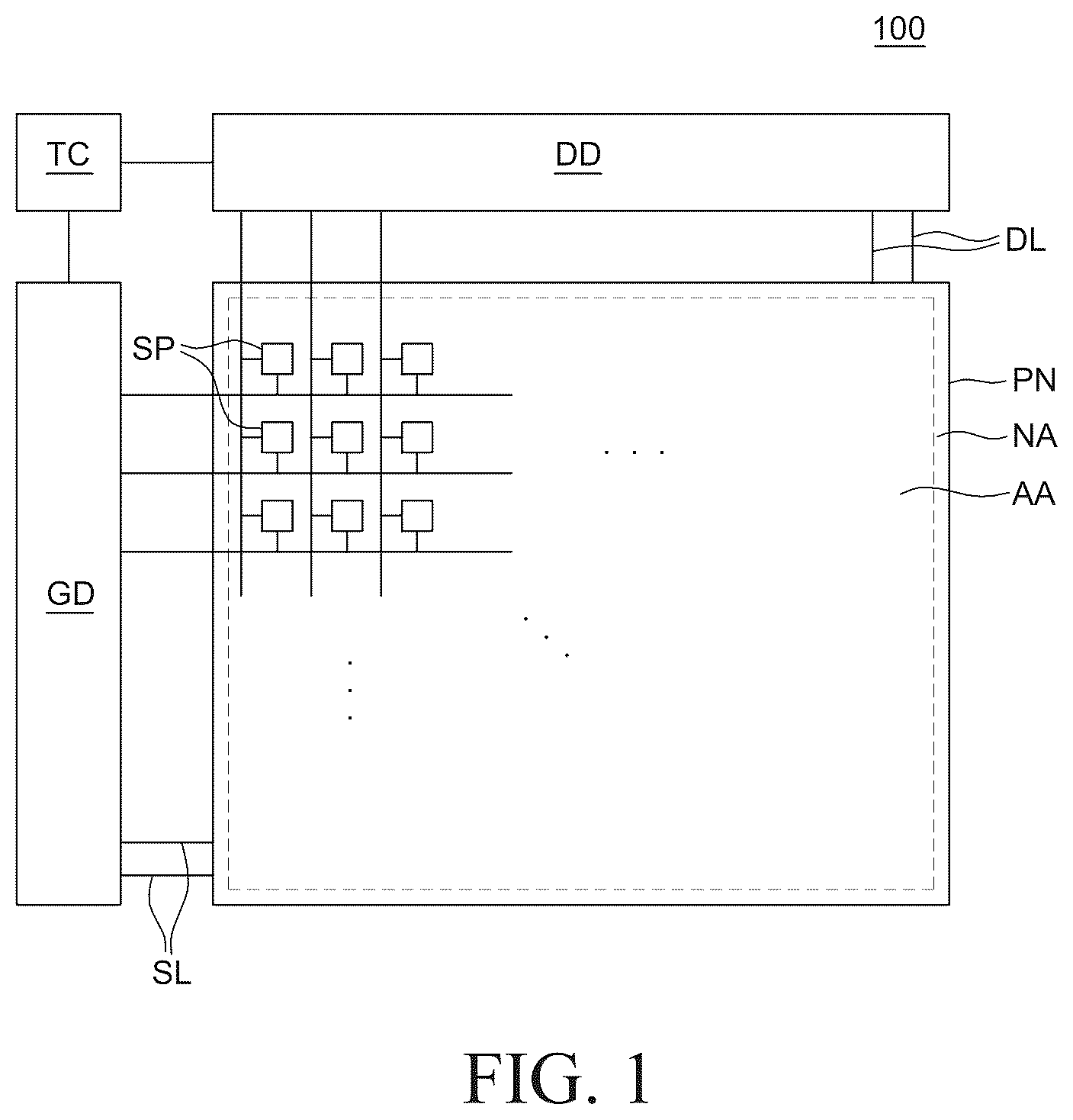
is a schematic diagram of a display device according to an exemplary embodiment of the present disclosure. In , for the convenience of description, among various components of the display device 100 , a display panel PN, a gate driver GD, a data driver DD, and a timing controller TC are illustrated.
Referring to , the display device 100 includes the display panel PN including a plurality of sub pixels SP, the gate driver GD and the data driver DD which supply various signals to the display panel PN, and the timing controller TC which controls the gate driver GD and the data driver DD.
The gate driver GD supplies a plurality of scan signals to a plurality of scan lines SL according to a plurality of gate control signals supplied from the timing controller TC. Even though in , it is illustrated that one gate driver GD is disposed to be spaced apart from one side of the display panel PN, the number of the gate drivers GD and the placement thereof are not limited thereto.
The data driver DD supplies a data voltage to a plurality of data lines DL according to a plurality of data control signals and image data supplied from the timing controller TC. The data driver DD may convert the image data into a data voltage using a reference gamma voltage and supply the converted data voltage to the plurality of data lines DL.
The timing controller TC aligns image data input from the outside to supply the image data to the data driver DD. The timing controller TC may generate a gate control signal and a data control signal using synchronization signals input from the outside, such as a dot clock signal, a data enable signal, and horizontal/vertical synchronization signals. The timing controller TC supplies the generated gate control signal and data control signal to the gate driver GD and the data driver DD, respectively, to control the gate driver GD and the data driver DD.
The display panel PN is a configuration which displays images to the user and includes the plurality of sub pixels SP. In the display panel PN, the plurality of scan lines SL and the plurality of data lines DL intersect each other and the plurality of sub pixels SP may be formed at intersections of the scan lines SL and the data lines DL.
In the display panel PN, an active area AA and a non-active area NA may be defined.
The active area AA is an area in which images are displayed in the display device 100 . In the active area AA, a plurality of sub pixels SP which configure a plurality of pixels and a pixel circuit for driving the plurality of sub pixels SP may be disposed. The plurality of sub pixels SP is a minimum unit which configures the active area AA and n sub pixels SP may form one pixel. In each of the plurality of sub pixels SP, a thin film transistor for driving the plurality of light emitting diodes EL may be disposed. The plurality of light emitting diodes EL may be defined in different ways depending on the type of the display panel PN. For example, when the display panel PN is an inorganic light emitting display panel PN, the light emitting diode EL may be a light emitting diode (LED) or a micro light emitting diode (micro-LED).
In the active area AA, a plurality of signal lines which transmit various signals to the plurality of sub pixels SP is disposed. For example, the plurality of signal lines may include a plurality of data lines DL which supplies a data voltage to each of the plurality of sub pixels SP and a plurality of scan lines SL which supplies a scan signal to each of the plurality of sub pixels SP. The plurality of scan lines SL extends to one direction in the active area AA to be connected to the plurality of sub pixels SP and the plurality of data lines DL extends to a direction different from the one direction in the active area AA to be connected to the plurality of sub pixels SP. In addition, in the active area AA, a low potential power line, a high potential power line, and the like may be further disposed, but are not limited thereto.
The non-active area NA is an area where images are not displayed so that the non-active area NA may be defined as an area extending from the active area AA. In the non-active area NA, a link line which transmits a signal to the sub pixel SP of the active area AA, a pad electrode, or a driving IC, such as a gate driver IC or a data driver IC, may be disposed.
In the meantime, the non-active area NA may be located on a rear surface of the display panel PN, that is, a surface on which the sub pixels SP are not disposed or may be omitted, and is not limited as illustrated in the drawing.
In the meantime, a driver, such as the gate driver GD, the data driver DD, and the timing controller TC, may be connected to the display panel PN in various ways. For example, the gate driver GD may be mounted in the non-active area NA in a gate in panel (GIP) manner or mounted between the plurality of sub pixels SP in the active area AA in a gate in active area (GIA) manner.
For example, the data driver DD and the timing controller TC are formed in separate flexible film and printed circuit board. The display panel PN may be electrically connected to the data driver DD and the timing controller TC by bonding the flexible film and the printed circuit board to the pad electrode formed in the non-active area NA of the display panel PN.
As another example, when the gate driver GD is mounted in the active area AA in the GIA manner and a side line which connects the signal line on the front surface of the display panel PN to the pad electrode on a rear surface of the display panel PN is formed to bond the flexible film and the printed circuit board onto a rear surface of the display panel PN, the non-active area NA may be minimized on the front surface of the display panel PN. Therefore, when the gate driver GD, the data driver DD, and the timing controller TC are connected to the display panel PN as described above, a zero bezel with substantially no bezel may be implemented.
Hereinafter, the plurality of sub pixels SP will be described in more detail with reference to .
is a schematic diagram of a sub pixel of a display device according to an exemplary embodiment of the present disclosure.
Referring to , the plurality of sub pixels SP includes a plurality of first sub pixels SP 1 , a plurality of second sub pixels SP 2 , and a plurality of third sub pixels SP 3 . Each of the plurality of sub pixels SP includes a light emitting diode EL and a pixel circuit to independently emit light. The plurality of sub pixels SP may include a first sub pixel SP 1 , a second sub pixel SP 2 , and a third sub pixel SP 3 which emit different color light. For example, the first sub pixel SP 1 is a red sub pixel that emits red light, the second sub pixel SP 2 is a green sub pixel that emits green light, and the third sub pixel SP 3 is a blue sub pixel that emits blue light, but it is not limited thereto.
The plurality of first sub pixels SP 1 may be disposed to form a plurality of columns and the plurality of second sub pixels SP 2 may be disposed in a column adjacent to a column in which the plurality of first sub pixels SP 1 is disposed. The plurality of third sub pixels SP 3 may be disposed in a column adjacent to columns in which the plurality of first sub pixels SP 1 and the plurality of second sub pixels SP 2 are disposed. That is, the plurality of first sub pixels SP 1 , the plurality of second sub pixels SP 2 , and the plurality of third sub pixels SP 3 may be disposed in different columns. Therefore, the plurality of sub pixels SP may be disposed such that the first sub pixels SP 1 , the second sub pixels SP 2 , and the third sub pixels SP 3 are repeatedly disposed in this order in a row direction.
In the meantime, the plurality of first sub pixels SP 1 , the plurality of second sub pixels SP 2 , and the plurality of third sub pixels SP 3 may form a plurality of first pixel groups GSP 1 , a plurality of second pixel groups GSP 2 , and a plurality of third pixel groups GSP 3 , respectively. Each of the plurality of pixel groups may be formed by n sub pixels SP. Each of the plurality of pixel groups may include n pulse width modulation (PWM) circuits and one pulse amplitude modulation (PAM) circuit.
In this case, each of the plurality of sub pixels SP includes a PWM circuit PWM, a PAM circuit PAM, and a light emitting diode EL and the PAM circuits PAM of the plurality of sub pixels SP are integrated into one so that the plurality of sub pixels SP may be defined to share one PAM circuit PAM. One pixel group configured by n sub pixels SP may be defined to include n PWM circuits PWM and one PAM circuit PAM (e.g., a single PAM circuit PAM). Thus, the display device includes a set of PWM circuits and a corresponding plurality of PWM circuits from the set are included in each pixel group.
The PWM circuit PWM is a circuit which expresses a gray scale level with a pulse width of a driving current. When the PWM circuit PWM is used, a time when the light emitting diode EL emits light is adjusted by configuring a pulse width of the driving current to be different to display images with various gray scale levels. At this time, the pulse width may be expressed by a duty ratio of a driving current or a duration of the driving current. For example, when an image with a low gray scale level is displayed, the PWM circuit PWM shortens a pulse width of the driving current, for example, shortens the duty ratio of the driving current or the duration of outputting the driving current to reduce the emission period of the light emitting diode EL and display the image with a low gray scale level. In contrast, when an image with a high gray scale level is displayed, the PWM circuit PWM increases a pulse width of the driving current, for example, increases the duty ratio of the driving current or the duration of outputting the driving current to increase the emission period of the light emitting diode EL and display the image with a high gray scale level.
The PAM circuit PAM is a circuit which expresses a gray scale level with an amplitude of a driving current. When the PAM circuit PAM is used, a time when the light emitting diode EL emits light is adjusted by configuring an amplitude of the driving current, that is, an intensity of the driving current to be different to display images with various gray scale levels. For example, when an image with a low gray scale level is displayed, the PAM circuit PAM lowers the intensity of the driving current to lower a luminance of light emitted from the light emitting diode EL and display an image with a low gray scale. In contrast, when an image with a high gray scale level is displayed, the PAM circuit PAM increases the intensity of the driving current to increase a luminance of light emitted from the light emitting diode EL and display an image with a high gray scale level.
Referring to again, each of the plurality of first pixel groups GSP 1 may include n first sub pixels SP 1 disposed in the same column. Each of the plurality of first pixel groups GSP 1 may include n first sub pixels SP 1 which are continuously disposed in the same column and each of n first sub pixels SP 1 may include a PAM circuit PAM and a PWM circuit PWM. In one embodiment, n first sub pixels SP 1 may share one PAM circuit PAM. Specifically, each of n first sub pixels SP 1 which form one first pixel group GSP 1 may include a corresponding PWM circuit PWM which independently operates from the other PWM circuits. At this time, n first sub pixels SP 1 may share one PAM circuit PAM. Therefore, one first sub pixel SP 1 includes one PAM circuit PAM and n PWM circuits PWM of n first sub pixels SP 1 may be connected to one PAM circuit PAM in parallel.
That is, in the first pixel group GSP 1 , n PWM circuits PWM and one PAM circuit PAM may be disposed to drive n first sub pixels SP 1 . For example, the first pixel group GSP 1 may include one PAM circuit PAM and a plurality of PWM circuits PWM and the plurality of PWM circuits PWM may include a first PWM circuit PWM 1 , a second PWM circuit PWM 2 , and a third PWM circuit PWM 3 .
At this time, an emission control transistor ET may be connected between each of the plurality of PWM circuits PWM and the PAM circuit PAM. For example, a first emission control transistor ET which is turned on or turned off by a first emission control signal EM 1 may be connected between the first PWM circuit PWM 1 and the PAM circuit PAM. A second emission control transistor ET which is turned on or turned off by a second emission control signal EM 2 may be connected between the second PWM circuit PWM 2 and the PAM circuit PAM. A third emission control transistor ET which is turned on or turned off by a third emission control signal EM 3 may be connected between the third PWM circuit PWM 3 and the PAM circuit PAM. The plurality of emission control transistors ET may control a driving timing of each of the plurality of PWM circuits PWM, which will be described in more detail with reference to .
The plurality of second pixel groups GSP 2 and the plurality of third pixel groups GSP 3 may be formed with the substantially same configuration as the plurality of first pixel groups GSP 1 .
Specifically, each of the plurality of second pixel groups GSP 2 may include n second sub pixels SP 2 disposed in the same column. Each of the plurality of second pixel groups GSP 2 may include n second sub pixels SP 2 which are continuously disposed in the same column and each of n second sub pixels SP 2 may include a PAM circuit PAM and a PWM circuit PWM. At this time, the PAM circuits PAM of n second sub pixels SP 2 are integrated so that n second sub pixels SP 2 may share one PAM circuit PAM. Specifically, each of n second sub pixels SP 2 which form one second pixel group GSP 2 may include PWM circuits PWM which independently operate. N second sub pixels SP 2 may share one PAM circuit PAM. Therefore, in one second pixel group GSP 2 , n PWM circuits PWM and one PAM circuit PAM may be disposed to drive n second sub pixels SP 2 .
Each of the plurality of third pixel groups GSP 3 may include n third sub pixels SP 3 disposed in the same column. Each of the plurality of third pixel groups GSP 3 may include n third sub pixels SP 3 which are continuously disposed in the same column and each of n third sub pixels SP 3 may include a PAM circuit PAM and a PWM circuit PWM. At this time, the PAM circuits PAM of n third sub pixels SP 3 are integrated so that n third sub pixels SP 3 may share one PAM circuit PAM. Specifically, each of n third sub pixels SP 3 which form one third pixel group GSP 3 may include a PWM circuit PWM which independently operates. N third sub pixels SP 3 may share one PAM circuit PAM. Therefore, in one third pixel group GSP 3 , n PWM circuits PWM and one PAM circuit PAM may be disposed to drive n third sub pixels SP 3 .
Even though in , it is illustrated that three sub pixels SP are included in one pixel group, this is illustrative and the number of sub pixels SP which are included in one pixel group is not limited thereto.
Hereinafter, a PAM circuit PAM and a PWM circuit PWM which form one pixel group will be described in detail with reference to .
is a circuit diagram of a first pixel group of a display device according to an exemplary embodiment of the present disclosure. Even though in , a circuit diagram of a first pixel group GSP 1 among the plurality of pixel groups is illustrated, circuit diagrams of the second pixel group GSP 2 and the third pixel group GSP 3 are the substantially same as the circuit diagram of the first pixel group GSP 1 .
Referring to , a plurality of transistors are disposed in one first pixel group GSP 1 . The plurality of transistors may be N-type transistors or P-type transistors. In the N-type transistor, carriers are electrons so that electrons may flow from the source electrode to the drain electrode and currents may flow from the drain electrode to the source electrode. In the P-type transistor, carriers are holes so that holes may flow from the source electrode to the drain electrode and currents may flow from the source electrode to the drain electrode. For example, one of the plurality of transistors may be an N-type transistor and the other one of the plurality of transistors may be a P-type transistor.
Hereinafter, it is assumed that the plurality of transistors is N-type transistors, but is not limited thereto.
First, the plurality of first sub pixels SP 1 which form one first pixel group GSP 1 shares one PAM circuit PAM. The PAM circuit PAM includes a first switching transistor ST 1 , a first driving transistor DT 1 , a first sensing transistor SST 1 , and a first capacitor C 1 . The PAM circuit PAM may be connected to a first data line, a first scan line, a sensing line, a reference line, and a high potential power line VDD.
The first switching transistor ST 1 is a transistor which is turned on by a first scan signal SCAN 1 to transmit a first data voltage Data_PAM to the first driving transistor DT 1 . A gate electrode of the first switching transistor ST 1 is connected to the first scan line, a drain electrode is connected to the first data line, and a source electrode is connected to a gate electrode of the first driving transistor DT 1 which is a first node N 1 . The first switching transistor ST 1 is turned on by the first scan signal SCAN 1 from the first scan line to transmit the first data voltage Data_PAM of the first data line to the gate electrode of the first driving transistor DT 1 .
The first driving transistor DT 1 is a transistor which controls an intensity of the driving current based on the first data voltage Data_PAM transmitted from the first switching transistor ST 1 . The gate electrode of the first driving transistor DT 1 is connected to the first node N 1 , a drain electrode is connected to the high potential power line VDD, and a source electrode is connected to a second node N 2 . A driving current of the PAM circuit PAM may be output from the first driving transistor DT 1 to each of the plurality of PWM circuits PWM.
The first sensing transistor SST 1 is a transistor which senses a threshold voltage of the first driving transistor DT 1 to compensate for a threshold voltage difference of the first driving transistor DT 1 . A gate electrode of the first sensing transistor SST 1 is connected to the sensing line, a drain electrode is connected to the reference line, and a source electrode is connected to the second node N 2 . The first sensing transistor SST 1 is turned on by a sensing signal Sense from the sensing line to connect the second node N 2 which is the source electrode of the first driving transistor DT 1 to the reference line.
Next, the first capacitor C 1 maintains a potential difference between the gate electrode and the source electrode of the first driving transistor DT 1 while the light emitting diode EL emits light to supply a constant driving current. The first capacitor C 1 includes a plurality of capacitor electrodes and a first capacitor electrode is connected to the first node N 1 and a second capacitor electrode is connected to the second node N 2 .
Next, each of the plurality of PWM circuits includes a second switching transistor ST 2 , a second driving transistor DT 2 , an emission control transistor ET, a second sensing transistor SST 2 , a third sensing transistor SST 3 , a second capacitor C 2 , and a third capacitor C 3 . The PWM circuit PWM may be connected to a second data line, a second scan line, a third scan line, the sensing line, the reference line, and a low potential power line VSS. Each of the plurality of PWM circuits PWM may be electrically connected to the second node N 2 which is an output terminal of the PAM circuit PAM from which a driving current is output. That is, a plurality of PWM circuits PWM may be connected to one PAM circuit PAM in parallel.
First, the second switching transistor ST 2 is a transistor which is turned on by a second scan signal SCAN 2 to transmit a second data voltage Data_PWM to the second driving transistor DT 2 . A gate electrode of the second switching transistor ST 2 is connected to the second scan line, a drain electrode is connected to the second data line, and a source electrode is connected to a gate electrode of the second driving transistor DT 2 which is a third node N 3 . The second switching transistor ST 2 is turned on by the second scan signal SCAN 2 from the second scan line to transmit the second data voltage Data_PWM of the second data line to the gate electrode of the second driving transistor DT 2 .
The second driving transistor DT 2 is a transistor which controls the driving current based on the second data voltage Data_PWM transmitted from the second switching transistor ST 2 . The gate electrode of the second driving transistor DT 2 is connected to the third node N 3 , a drain electrode is connected to a fourth node N 4 , and a source electrode is connected to a fifth node N 5 . The second driving transistor DT 2 is turned on to supply the driving current to the light emitting diode EL.
The second sensing transistor SST 2 is a transistor which senses a threshold voltage of the second driving transistor DT 2 to compensate for a threshold voltage difference of the second driving transistor DT 2 . A gate electrode of the second sensing transistor SST 2 is connected to the sensing line, a drain electrode is connected to the reference line, and a source electrode is connected to the fifth node N 5 . The second sensing transistor SST 2 is turned on by a sensing signal Sense from the sensing line to connect the fifth node N 5 which is the source electrode of the second driving transistor DT 2 to the reference line.
The emission control transistor ET is a transistor which blocks or connects a path through which the driving current flows between the PAM circuit PAM and the PWM circuit PWM. A gate electrode of the emission control transistor ET is connected to the emission control line, a drain electrode is connected to the second node N 2 which is an output terminal of the PAM circuit PAM, and a source electrode is connected to the fourth node N 4 which is the drain electrode of the second driving transistor DT 2 . The emission control transistor ET is turned on by the emission control signal EM from the emission control line to transmit the driving current from the PAM circuit PAM to the second driving transistor DT 2 .
At this time, the emission control transistor ET of each of the plurality of PWM circuits PWM may be connected to a different emission control line. Each of the plurality of PWM circuits PWM is connected to a different emission control line to independently control an emission period of the light emitting diode EL connected to each of the plurality of PWM circuits PWM. That is, the emission period of each of the plurality of PWM circuits PWM may be separately controlled. For example, one emission control transistor ET of emission control transistors ET of three PWM circuits PWM is connected to a first emission control line to be applied with a first emission control signal EM 1 . Another emission control transistor ET is connected to a second emission control line to be applied with a second emission control signal EM 2 . The other emission control transistor ET is connected to a third emission control line to be applied with a third emission control signal EM 3 . Accordingly, the first emission control signal EM 1 , the second emission control signal EM 2 , and the third emission control signal EM 3 are applied to the first emission control line, the second emission control line, and the third emission control line, respectively. Therefore, turning-on and turning-off operations of the emission control transistors ET of the plurality of PWM circuits PWM may be independently controlled.
In the meantime, in the present disclosure, the PWM circuits PWM are referred to as a plurality of PWM circuits PWM without distinction. However, the plurality of PWM circuits PWM may be separately defined as a first PWM circuit connected to the first emission control line, a second PWM circuit connected to the second emission control line, and a third PWM circuit connected to the third emission control line, but is not limited thereto.
Next, the third sensing transistor SST 3 is a transistor which supplies a voltage to the drain electrode of the second driving transistor DT 2 when the threshold voltage of the second driving transistor DT 2 is sensed. A gate electrode of the third sensing transistor SST 3 is connected to the third scan line, a drain electrode is connected to the sensing voltage line, and a source electrode is connected to the drain electrode of the second driving transistor DT 2 which is the fourth node N 4 . The third sensing transistor SST 3 is turned on by a third scan signal SCAN 3 of the third scan line and transmits a sensing voltage V_sense to the drain electrode of the second driving transistor DT 2 . A sensing current may flow from the drain electrode of the second driving transistor DT 2 to the source electrode by the sensing voltage V_sense. The second sensing transistor SST 2 transmits the sensing current to the reference line to sense the threshold voltage of the second driving transistor DT 2 . Specifically, the drain electrode of the first driving transistor DT 1 is connected to the high potential power line VDD so that even though the third sensing transistor SST 3 is not connected, the sensing current may flow. However, the drain electrode of the second driving transistors DT 2 is not connected to a separate power line so that the sensing current may not flow in the second driving transistor, like the first driving transistor DT 1 . Therefore, only when the third sensing transistor SST 3 is connected to the drain electrode of the second driving transistor DT 2 to sense the threshold voltage, the sensing voltage V_sense is supplied to the drain electrode of the second driving transistor DT 2 to flow the sensing current.
In the meantime, one third sensing transistor SST 3 may be connected to the fourth node N 4 of each of the plurality of PWM circuits PWM. That is, the plurality of PWM circuits PWM may share one third sensing transistor SST 3 . Therefore, the plurality of PWM circuits PWM includes one third sensing transistor SST 3 to reduce the number of overall transistors and simply the design.
The second capacitor C 2 is a capacitor which is connected between a sweep line and the third node N 3 to transmit a sweep signal Sweep of the sweep line to the third node N 3 . The second capacitor C 2 includes a plurality of capacitor electrodes and a first capacitor electrode is connected to the sweep line and a second capacitor electrode is connected to the third node N 3 which is the gate electrode of the second driving transistor DT 2 . The sweep signal Sweep which is applied to the sweep line linearly changes. During the emission period, when the sweep signal Sweep is applied to one end of the second capacitor C 2 , a coupling voltage may be generated in the gate electrode of the second driving transistor DT 2 which is floated. Accordingly, the voltage of the gate electrode of the second driving transistor DT 2 is coupled to the sweep signal Sweep to be decreased or increased and the second driving transistor DT 2 may be turned off or turned on.
The third capacitor C 3 maintains a potential difference between the gate electrode and the source electrode of the second driving transistor DT 2 while the light emitting diode EL emits light to supply a constant driving current. The third capacitor C 3 includes a plurality of capacitor electrodes and a first capacitor electrode is connected to the third node N 3 and a second capacitor electrode is connected to the fifth node N 5 .
Next, the light emitting diode EL is connected to the fifth node N 5 of each of the plurality of PWM circuits PWM. The light emitting diode EL includes an anode and a cathode. The anode of the light emitting diode EL is connected to the fifth node N 5 and the cathode is connected to the low potential power line VSS to which a low potential power voltage is supplied. Accordingly, the light emitting diode EL may emit light based on a driving current which is transmitted from the second driving transistor DT 2 to the anode.
In the meantime, a micro-LED which has excellent luminous efficiency may be mainly used as the light emitting diode EL. In the micro-LED, the color coordinate is distorted in a low current band. When a driving current in the low current band is supplied to the light emitting diode EL according to a characteristic of an image to be displayed, the color coordinate of the light emitting diode EL is distorted to degrade an image display quality.
Accordingly, in the display device 100 according to the exemplary embodiment of the present disclosure, the first data voltage Data_PAM having a constant value is applied to the PAM circuit PAM. Therefore, the color coordinate distortion of the light emitting diode EL which is generated in the low current band may be suppressed and the light emitting diode EL may be stably driven. The PAM circuit is a circuit configured to adjust an amplitude of the driving current, that is, an intensity of the driving current. If only a first data voltage Data_PAM with a specific value is applied to the PAM circuit PAM, the PAM circuit PAM may generate a driving current which always has a constant intensity and output the driving current to the PWM circuit PWM. That is, the PAM circuit PAM may generate and output a driving current which is always constant regardless of the gray scale level of the displayed image. At this time, a first data voltage Data_PAM may be set to fix a driving current which is primarily generated in the PAM circuit PAM as a current excluding the low current band. Accordingly, the first data voltage Data_PAM is fixed to a specific value to supply a driving current which has always a constant intensity to the light emitting diode EL so that the color coordinate distortion may not occur.
At this time, the first data voltage Data_PAM applied to the PAM circuit may be determined according to an efficiency of the light emitting diode EL of a pixel group in which the PAM circuit PAM is disposed. That is, the first data voltage Data_PAM has a constant value that is dependent on the color of the light emitting diodes EL of the pixel group. A different type of light emitting diode EL may be disposed in each of the first sub pixel SP 1 , the second sub pixel SP 2 , and the third sub pixel SP 3 . For example, in the first sub pixel SP 1 which is a red sub pixel SP, a red light emitting diode which emits red light may be disposed. In the second sub pixel SP 2 which is a green sub pixel SP, a green light emitting diode which emits green light may be disposed. In the third sub pixel SP 3 which is a blue sub pixel SP, a blue light emitting diode which emits blue light may be disposed. The red light emitting diode, the green light emitting diode, and the blue light emitting diode which emit different colors of light have different efficiencies so that even though the driving current with the same intensity is supplied, the luminance of light emitted from the red light emitting diode, the green light emitting diode, and the blue light emitting diode may be different. Therefore, the first data voltage Data_PAM supplied to the PAM circuit PAM of each of the first pixel group GSP 1 , the second pixel group GSP 2 , and the third pixel group GSP 3 may be determined in consideration of the characteristic of the light emitting diode EL of each pixel group.
In the meantime, when a PAM circuit PAM which generates a driving current always having a constant intensity is used, it may be difficult to express various gray scale levels. Accordingly, in the display device 100 according to the exemplary embodiment of the present disclosure, a PWM circuit PWM which controls a pulse width of the driving current is used together to display images with various gray scale levels. The PWM circuit PWM is connected between the PAM circuit PAM and the light emitting diode EL to adjust a duty ratio or a duration that the driving current generated in the PAM circuit PAM is supplied to the light emitting diode EL. The PWM circuit PWM adjusts the duty ratio or the duration that the driving current is supplied to the light emitting diode EL to display images with various gray scale levels. At this time, a second data voltage Data_PWM applied to the PWM circuit PWM may vary depending on the gray scale level, unlike the first data voltage Data_PAM. For example, a value of the second data voltage Data_PWM which is output for the low-gray scale image and a value of the second data voltage Data_PWM which is output for a high-gray scale image may be different. The PWM circuit PWM may adjust the emission time of the light emitting diode EL based on the second data voltage Data_PWM to be different. Thus, the magnitude of the second data voltage Data_PWM is image dependent. For example, the second data voltage Data_PWM may have a first magnitude that corresponds to a first image at a first time such that the driving current is supplied to the second driving transistor DT 2 for a first duration and the second data voltage Data_PWM has a second magnitude that corresponds to a second image at a second time such that the driving current is supplied to the second driving transistor DT 2 for a second duration that is different from the first duration. Accordingly, the display device 100 according to the exemplary embodiment of the present disclosure uses the PAM circuit PAM and the PWM circuit PWM together to stably drive the light emitting diode EL and improve a display quality of the image while suppressing the color coordinate distortion in the low current band. The PAM circuit PAM generates a driving current with a constant intensity in a band other than the low current band and the PWM circuit PWM adjusts the pulse width of the driving current generated in the PAM circuit to supply the driving current to the light emitting diode EL to express the gray scale level.
Hereinafter, a driving process of the sub pixel SP of the display device 100 according to the exemplary embodiment of the present disclosure will be described in more detail with reference to A to 5 C .
A to 4 C are driving timing diagrams of a sub pixel of a display device according to an exemplary embodiment of the present disclosure. A is a circuit diagram of a first pixel group of a display device during an initialization period according to an exemplary embodiment of the present disclosure. B is a circuit diagram of a first pixel group of a display device during a data writing period according to an exemplary embodiment of the present disclosure. C is a circuit diagram of a first pixel group of a display device during an emission period according to an exemplary embodiment of the present disclosure.
Referring to A , the plurality of sub pixels SP of the display device 100 according to the exemplary embodiment of the present disclosure may be driven in the order of the initialization period, the data writing period, and the emission period. A period between a time A and a time B is the initialization period, a period between a time B and a time D is the data writing period, and the emission period is after the time D.
In the meantime, each of the plurality of PWM circuits is connected to different sweep line, second scan line, and sensing line so that the driving timings of the initialization period and the data writing period may be independently controlled. For example, the first PWM circuit is connected to n-th lines, among the plurality of lines to be applied with an n-th sweep signal Sweep (n), an n-th second scan signal SCAN 2 ( n ), and an n-th sensing signal Sense (n). The second PWM circuit is connected to n+1-th lines, among the plurality of lines to be applied with an n+1-th sweep signal Sweep (n+1), an n+1-th second scan signal SCAN 2 (n+1), and an n+1-th sensing signal Sense (n+1). The third PWM circuit is connected to n+2-th lines, among the plurality of lines to be applied with an n+2-th sweep signal Sweep (n+2), an n+2-th second scan signal SCAN 2 (n+2), and an n+2-th sensing signal Sense (n+2). At this time, the driving timings of the initialization period and the data writing period of each of the first PWM circuit, the second PWM circuit, and the third PWM circuit may be determined according to a timing when a signal is output to each of the n-th line, the n+1-th line, and the n+2-th line.
In A , for the convenience of description, the description will be made as follows: An n-th sweep signal Sweep (n), an n+1-th sweep signal Sweep (n+1), and an n+2-th sweep signal Sweep (n+2) are illustrated to be unified as one sweep signal Sweep. An n-th second scan signal SCAN 2 ( n ), an n+1-th second scan signal SCAN 2 (n+1), and an n+2-th second scan signal SCAN 2 (n+2) are illustrated to be unified as one second scan signal SCAN 2 . An n-th sensing signal Sense (n), an n+1-th sensing signal Sense (n+1), and an n+2-th sensing signal Sense (n+2) are illustrated to be unified as one sensing signal Sense. Further, all the plurality of PWM circuits PWM is applied with the second data voltage Data_PWM at the same timing. However, each of the plurality of PWM circuits PWM may be applied with a second data voltage Data_PWM at different timings, but it is not limited thereto.
Referring to A and 5 A together, during the initialization period between the times A and B, a high level of sensing signal Sense is output to the sensing line. Therefore, the first sensing transistor SST 1 and the second sensing transistor SST 2 connected to the sensing line through the gate electrodes are turned on to apply the reference voltage Vref to the second node N 2 and the fourth node N 4 . Accordingly, the source electrode of the first driving transistor DT 1 of the PAM circuit PAM and the source electrode of the second driving transistor DT 2 of the PWM circuit PWM may be initialized to the reference voltage Vref.
Referring to A and 5 B together, during the data writing period between the times B and D, a high level of first scan signal SCAN 1 is output to the first scan line and a high level of second scan signal SCAN 2 is output to the second scan line. The first switching transistor ST 1 of the PAM circuit PAM is turned on by the first scan signal SCAN 1 to transmit the first data voltage Data_PAM to the first node N 1 . The second switching transistor ST 2 of the PWM circuit PWM is turned on by the second scan signal SCAN 2 to transmit the second data voltage Data_PWM to the third node N 3 .
In the meantime, in the present disclosure, it is described that the first scan signal SCAN 1 and the second scan signal SCAN 2 are output in different periods to configure periods where the data voltages are written in the PAM circuit PAM and the PWM circuit PWM to be different. However, the data voltages may be simultaneously written in the PAM circuit PAM and the PWM circuit PWM, but it is not limited thereto.
Next, referring to A and 5 C , during the emission period after the time D, a high level of emission control signal EM is output to the emission control line. Accordingly, the driving current from the PAM circuit PAM may flow to the second driving transistor DT 2 of the PWM circuit PWM through the turned-on emission control transistor ET. The second driving transistor DT 2 may transmit the driving current to the light emitting diode EL according to the sweep signal Sweep applied to the gate electrode. Finally, the light emitting diode EL may be supplied with the driving current from the first driving transistor DT 1 and the second driving transistor DT 2 to emit light.
The second driving transistor DT 2 may determine a length of a period when the light emitting diode EL actually emits light within a period when the emission control transistor ET is turned on. The actual emission period of the light emitting diode EL may correspond to a period when the second driving transistor DT 2 is turned on in the period when the emission control transistor ET is turned on. For example, even though the emission control transistor ET is turned on, the second driving transistor DT 2 may be turned off to control the light emitting diode EL so as not to emit light. As another example, only in a partial period of the period when the emission control transistor ET is turned on, the second driving transistor DT 2 is turned on to control the light emitting diode EL so as to emit light only during a partial period.
In the meantime, the emission signal may be output to the emission control line in various orders. For example, referring to B , a plurality of pixel groups is disposed to form a plurality of rows and an emission control signal EM including a first emission control signal EM 1 , a second emission control signal EM 2 , and a third emission control signal EM 3 may be sequentially applied to the pixel groups, starting from a pixel group in an uppermost row. The first emission control signal EM 1 , the second emission control signal EM 2 , and the third emission control signal EM 3 may be sequentially applied to the first emission control line, the second emission control line, and the third emission control line connected to pixel groups in a first row. The first emission control signal EM 1 , the second emission control signal EM 2 , and the third emission control signal EM 3 may be sequentially applied to the first emission control line, the second emission control line, and the third emission control line connected to pixel groups in a second row. Finally, the first emission control signal EM 1 , the second emission control signal EM 2 , and the third emission control signal EM 3 may be applied to the first emission control line, the second emission control line, and the third emission control line connected to pixel groups in a lowermost row. Accordingly, the plurality of sub pixels SP which is disposed to form a plurality of rows, may emit light sequentially in the order from a sub pixel SP in the uppermost row to a sub pixel SP in the lowermost row.
As another example, referring to C , the first emission control signal EM 1 may be applied first to the first emission control line of each of the plurality of pixel groups. In this case, among three sub pixels SP included in each of the plurality of pixel groups, only a sub pixel SP connected to the first emission control line may emit light first. Next, the second emission control signal EM 2 may be applied to the second emission control line of each of the plurality of pixel groups. Therefore, a sub pixel SP connected to the second emission control line may emit light. Finally, the third emission control signal EM 3 may be connected to the third emission control line of each of the plurality of pixel groups. Accordingly, among three sub pixels SP included in each of the plurality of pixel groups, a sub pixel SP connected to the third emission control line may emit light last.
Accordingly, in the display device 100 according to the exemplary embodiment of the present disclosure, the plurality of sub pixels SP shares one PAM circuit PAM to reduce the number of transistors. That is, one PWM circuit PWM is disposed in each of the plurality of sub pixels SP and the plurality of PWM circuits PWM is connected to an output terminal of the one PAM circuit PAM in parallel to drive the light emitting diode EL. Accordingly, a PAM circuit PAM which is individually disposed in each of the plurality of sub pixels SP is deleted to reduce the number of overall transistors. Therefore, a design area occupied by one sub pixel SP may be reduced and a larger number of sub pixels SP may be formed in the same area. Accordingly, a design area of each of the plurality of sub pixels SP is reduced to implement a display device 100 with a high resolution.
Hereinafter, an external compensation process of a PAM circuit PAM and a PWM circuit PWM will be described with reference to to 9 .
is a timing diagram of external compensation of a PAM circuit of a display device according to an exemplary embodiment of the present disclosure. is a circuit diagram of a first pixel group of a display device during an external compensation period of a PAM circuit according to an exemplary embodiment of the present disclosure. is a timing diagram of external compensation of a PWM circuit of a display device according to an exemplary embodiment of the present disclosure. is a circuit diagram of a first pixel group of a display device during an external compensation period of a PWM circuit according to an exemplary embodiment of the present disclosure.
In the display device 100 according to the exemplary embodiment of the present disclosure, threshold voltages of a first driving transistor DT 1 of a PAM circuit PAM and a second driving transistor DT 2 of a PWM circuit PWM may be sensed and compensated by an external compensation method using a source follower. The threshold voltage may be sensed and compensated in a state when the display device 100 is turned off and the threshold voltage of the first driving transistor DT 1 of the PAM circuit PAM and the threshold voltage of the second driving transistor DT 2 of the PWM circuit PWM may be sensed in different periods.
First, referring to , the threshold voltage of the first driving transistor DT 1 of the PAM circuit PAM may be sensed in the order of an initialization period, a source following period, and a sampling period. A period between a time A and a time B is the initialization period, a period between a time B and a time C is the source following period, and the sampling period is after the time C.
During the initialization period between the times A and B, a voltage of the source electrode of the first driving transistor DT 1 of the PAM circuit PAM may be initialized. At the time A, a high level of sensing signal Sense is applied to the sensing line to turn on the first sensing transistor SST 1 and connect the reference line and the second node N 2 which is the source electrode of the first driving transistor DT 1 . Accordingly, at the time A, the voltage of the source electrode of the first driving transistor DT 1 may be initialized.
Next, during the source following period between the times B and C, the sensing current may flow while holding the voltage of the gate electrode of the first driving transistor DT 1 of the PAM circuit PAM. At the time B, a high level of first scan signal SCAN 1 is output to the first scan line to apply a sensing data voltage to the gate electrode of the first driving transistor DT 1 . The sensing current may flow from the drain electrode to the source electrode of the first driving transistor DT 1 and a voltage of the source electrode of the first driving transistor DT 1 may gradually increase. The sensing current which flows through the first driving transistor DT 1 may flow until a potential difference between the source electrode and the gate electrode of the first driving transistor DT 1 is equal to a threshold voltage.
Finally, during the sampling period after the time C, a high level of sensing signal Sense is output to the sensing line to turn on the first sensing transistor SST 1 . When the sensing current does not flow, an analog to digital converter may detect a voltage of the source electrode of the first driving transistor DT 1 through the turned-on first sensing transistor SST 1 and the reference line. Accordingly, the threshold voltage of the first driving transistor DT 1 may be detected from the sensing data voltage applied to the gate electrode of the first driving transistor DT 1 and the voltage of the source electrode of the first driving transistor DT 1 . Accordingly, the data driver DD compensates for the first data voltage Data_PAM based on the threshold voltage of the first driving transistor DT 1 to output the compensated voltage to the sub pixel SP.
Next, referring to , the threshold voltage of the second driving transistor DT 2 of the PWM circuit PWM may be sensed in the order of an initialization period, a source following period, and a sampling period. A period between a time A and a time B is the initialization period, a period between a time B and a time C is the source following period, and the sampling period is after the time C.
During the initialization period between the times A and B, a voltage of the source electrode of the second driving transistor DT 2 of the PWM circuit PWM may be initialized. At the time A, a high level of sensing signal Sense is applied to the sensing line to turn on the second sensing transistor SST 2 and connect the reference line and the fifth node N 5 which is the source electrode of the second driving transistor DT 2 . Accordingly, at the time A, the voltage of the source electrode of the second driving transistor DT 2 may be initialized.
Next, during the source following period between the times B and C, the voltage of the gate electrode of the second driving transistor DT 2 of the PWM circuit PWM is held for the sensing data voltage and the sensing voltage V_sense is applied to the drain electrode to flow a sensing current in the second driving transistor DT 2 . At the time B, a high level of second scan signal SCAN 2 is output to the second scan line to apply a sensing data voltage to the gate electrode of the second driving transistor DT 2 . A high level of third scan signal SCAN 3 is output to the third scan line to turn on the third sensing transistor SST 3 . During the entire period when the threshold voltage is sensed, the third scan line may continuously output the high level of third scan signal SCAN 3 and the sensing voltage V_sense may be applied to the fourth node N 4 which is the drain electrode of the second driving transistor DT 2 . Accordingly, the sensing current may flow from the drain electrode to the source electrode of the second driving transistor DT 2 and a voltage of the source electrode of the second driving transistor DT 2 may gradually increase. The sensing current which flows through the second driving transistor DT 2 may flow until a potential difference between the source electrode and the gate electrode of the second driving transistor DT 2 is equal to a threshold voltage.
Finally, during the sampling period after the time C, a high level of sensing signal Sense is output to the sensing line to turn on the second sensing transistor SST 2 . The analog to digital converter may detect a voltage of the source electrode of the second driving transistor DT 2 through the turned-on second sensing transistor SST 2 and the reference line. Accordingly, the threshold voltage of the second driving transistor DT 2 may be detected from the sensing data voltage applied to the gate electrode of the second driving transistor DT 2 and the voltage of the source electrode of the second driving transistor DT 2 . Accordingly, the data driver DD compensates for the second data voltage Data_PWM based on the threshold voltage of the second driving transistor DT 2 to output the compensated voltage to the sub pixel SP.
Accordingly, in the display device 100 according to the exemplary embodiment of the present disclosure, the threshold voltage of the first driving transistor DT 1 of the PAM circuit PAM may be sensed using the first sensing transistor SST 1 . Further, the threshold voltage of the second driving transistor DT 2 of the PWM circuit PWM may be sensed using the second sensing transistor SST 2 and the third sensing transistor SST 3 . Therefore, the threshold voltage difference between the plurality of sub pixels SP is compensated to apply the first data voltage Data_PAM and the second data voltage Data_PWM to improve the luminance uniformity and improve the display quality of the image.
is a circuit diagram of a first pixel group of a display device according to another exemplary embodiment of the present disclosure. A display device 1000 of includes a circuit which senses and compensates for threshold voltages of the first driving transistor DT 1 of the PAM circuit PAM and the second driving transistor DT 2 of the PWM circuit PWM by an internal compensation method. This is different from the circuit configuration of the sub pixel SP of the display device 100 of to 9 . However, another configuration is substantially the same so that a redundant description will be omitted. Even though in , only a circuit diagram of a first pixel group GSP 1 among the plurality of pixel groups is illustrated, circuits of the second pixel group GSP 2 and the third pixel group GSP 3 are the substantially same as the circuit of the first pixel group GSP 1 .
Referring to , a plurality of transistors are disposed in one first pixel group GSP 1 . The plurality of transistors may be N-type transistors in which a current flows from drain electrodes to source electrodes or P-type transistors in which a current flows from source electrodes to drain electrodes. Hereinafter, it is assumed that the plurality of transistors is P-type transistors, but is not limited thereto.
The plurality of first sub pixels SP 1 which form one first pixel group GSP 1 shares one PAM circuit PAM. The PAM circuit PAM includes a first switching transistor ST 1 , a second switching transistor ST 2 , a third switching transistor ST 3 , a fourth switching transistor ST 4 , a first driving transistor DT 1 , a first emission control transistor ET 1 , and a first capacitor C 1 . The PAM circuit PAM is connected to a first data line, a first scan line, a second scan line, a first emission control line, a reference line, and a high potential power line VDD.
The first switching transistor ST 1 is a transistor which is turned on by a first scan signal SCAN 1 to transmit a first data voltage Data_PAM to an internal configuration of the PAM circuit PAM. A gate electrode of the first switching transistor ST 1 is connected to the first scan line, a source electrode is connected to the first data line, and a drain electrode is connected to the first capacitor C 1 at a first node N 1 . The first switching transistor ST 1 is turned on by the first scan signal SCAN 1 from the first scan line to transmit the first data voltage Data_PAM of the first data line to the first capacitor C 1 .
The second switching transistor ST 2 is a transistor which samples the threshold voltage of the first driving transistor DT 1 to compensate for a threshold voltage difference between the first driving transistors DT 1 of the plurality of sub pixels SP. A gate electrode of the second switching transistor ST 2 is connected to the second scan line and a source electrode and a drain electrode are connected to the second node N 2 and the third node N 3 , respectively. The second switching transistor ST 2 shorts the gate electrode and the drain electrode of the first driving transistor DT 1 and may form diode connection of the first driving transistor DT 1 . In the diode connection, the gate electrode and the drain electrode are shorted so that the transistor operates as a diode.
The third switching transistor ST 3 is a transistor for transmitting the reference voltage Vref to the first node N 1 . A gate electrode of the third switching transistor ST 3 is connected to the first emission control line, a source electrode is connected to the reference line, and a drain electrode is connected to the first node N 1 . The third switching transistor ST 3 may transmit the reference voltage Vref to the first node N 1 while applying a low level of first emission control signal EM 1 from the first emission control line and the first node N 1 may be initialized to the reference voltage Vref.
The fourth switching transistor ST 4 is a transistor for transmitting the reference voltage Vref to the fourth node N 4 . A gate electrode of the fourth switching transistor ST 4 is connected to the second scan line, a source electrode is connected to the reference line, and a drain electrode is connected to the fourth node N 4 . The fourth switching transistor ST 4 is turned on by the second scan signal SCAN 2 to transmit the reference voltage Vref to the fourth node N 4 . The reference voltage Vref of the fourth node N 4 may be transmitted to the third node N 3 which is the drain electrode of the first driving transistor DT 1 through the first emission control transistor ET 1 which is turned on together with the fourth switching transistor ST 4 . The voltages of the gate electrode and the drain electrode of the first driving transistor DT 1 may be initialized using the third switching transistor ST 3 and the fourth switching transistor ST 4 , which will be described in more detail with reference to A to 12 F .
The first driving transistor DT 1 is a transistor which controls an intensity of the driving current based on the first data voltage Data_PAM. The gate electrode of the first driving transistor DT 1 is connected to the second node N 2 , the source electrode is connected to the high potential power line VDD, and the drain electrode is connected to the third node N 3 . A driving current of the PAM circuit PAM may be output from the first driving transistor DT 1 to each of the plurality of PWM circuits PWM.
The first emission control transistor ET 1 is a transistor for transmitting the driving current from the first driving transistor DT 1 to each of the plurality of PWM circuits PWM. A gate electrode of the first emission control transistor ET 1 is connected to the first emission control line, a source electrode is connected to the third node N 3 , and a drain electrode is connected to the fourth node N 4 . The first emission control transistor is turned on to transmit the reference voltage Vref from the fourth switching transistor ST 4 to the drain electrode of the first driving transistor DT 1 or transmit the driving current from the first driving transistor DT 1 to each of the plurality of PWM circuits PWM.
The first capacitor C 1 maintains a potential difference between the gate electrode and the drain electrode of the first driving transistor DT 1 while the light emitting diode EL emits light to supply a constant driving current. The first capacitor C 1 includes a plurality of capacitor electrodes and a first capacitor electrode is connected to the first node N 1 and the a second capacitor electrode is connected to the second node N 2 .
Next, the plurality of first sub pixels SP 1 includes a plurality of PWM circuits PWM. Each of the plurality of PWM circuits PWM includes a fifth switching transistor ST 5 , a sixth switching transistor ST 6 , a second driving transistor DT 2 , a second emission control transistor ET 2 , and a second capacitor C 2 . The plurality of PWM circuits PWM may share and include one initialization transistor IT. The PWM circuit PWM is connected to a second data line, a third scan line, a second emission control line, a sweep line, an initialization line, and a low potential power line VSS. Each of the plurality of PWM circuits PWM may be electrically connected to the fourth node N 4 which is an output terminal of the PAM circuit PAM from which the driving current is output. That is, a plurality of PWM circuits PWM may be connected to one PAM circuit PAM in parallel.
The fifth switching transistor ST 5 is a transistor which is turned on by a third scan signal SCAN 3 to transmit a second data voltage Data_PWM to the second driving transistor DT 2 . A gate electrode of the fifth switching transistor ST 5 is connected to the third scan line, a source electrode is connected to the second data line, and a drain electrode is connected to the fifth node N 5 . The fifth switching transistor ST 5 is turned on by the third scan signal SCAN 3 from the third scan line to transmit the second data voltage Data_PWM of the second data line to the fifth node N 5 which is the source electrode of the second driving transistor DT 2 .
The sixth switching transistor ST 6 is a transistor which samples the threshold voltage of the second driving transistor DT 2 to compensate for a threshold voltage difference of the second driving transistors DT 2 of the plurality of sub pixels SP. A gate electrode of the sixth transistor ST 6 is connected to the third scan line and a source electrode and a drain electrode are connected to a sixth node N 6 and a seventh node N 7 . The sixth switching transistor ST 6 shorts the gate electrode and the drain electrode of the second driving transistor DT 2 and form diode connection of the second driving transistor DT 2 .
The second driving transistor DT 2 is a transistor which controls the driving current based on the second data voltage Data_PWM. The gate electrode of the second driving transistor DT 2 is connected to the sixth node N 6 , the source electrode is connected to the fifth node N 5 , and the drain electrode is connected to the seventh node N 7 . The second driving transistor DT 2 is turned on to supply the driving current to the light emitting diode EL.
The second emission control transistor ET 2 is a transistor which blocks or connects a path through which the driving current flows between the PAM circuit PAM and the PWM circuit PWM. A gate electrode of the second emission control transistor ET 2 is connected to any one of the second emission control line, the third emission control line, and the fourth emission control line and a source electrode is connected to the fourth node N 4 which is an output terminal of the PAM circuit PAM. Further, a drain electrode is connected to the fifth node N 5 which is the source electrode of the second driving transistor DT 2 . The second emission control transistor ET 2 is turned on by a second emission control signal EM 2 from the second emission control line to transmit the driving current from the PAM circuit PAM to the second driving transistor DT 2 .
The second emission control transistor ET 2 of each of the plurality of PWM circuits PWM may be connected to a different emission control line. Each of the plurality of PWM circuits PWM is connected to a different emission control line to independently control an emission period of the light emitting diode EL connected to each of the plurality of PWM circuits PWM. That is, the emission period of each of the plurality of PWM circuits PWM may be separately controlled. For example, a second emission control transistor ET 2 of a first PWM circuit PWM 1 among three PWM circuits PWM is connected to the second emission control line to be applied with the second emission control signal EM 2 . A second emission control transistor ET 2 of a second PWM circuit PWM 2 among three PWM circuits PWM is connected to the third emission control line to be applied with the third emission control signal EM 3 . A second emission control transistor ET 2 of a third PWM circuit PWM 3 among three PWM circuits PWM is connected to the fourth emission control line to be applied with the fourth emission control signal EM 4 . Accordingly, the second emission control signal EM 2 , the third emission control signal EM 3 , and the fourth emission control signal EM 4 are applied to the second emission control line, the third emission control line, and the fourth emission control line, respectively. Therefore, turning-on and turning-off operations of the second emission control transistors ET of the plurality of PWM circuits PWM may be independently controlled.
The second capacitor C 2 is a capacitor which transmits a sweep signal of the sweep line to the sixth node N 6 which is the gate electrode of the second driving transistor DT 2 . The second capacitor C 2 includes a plurality of second capacitor C 2 electrodes and a first second capacitor C 2 electrode is connected to the sweep line and a second capacitor C 2 electrode is connected to the third node N 3 which is the gate electrode of the second driving transistor DT 2 . When the sweep signal is applied to one end of the second capacitor C 2 , a coupling voltage may generate in the gate electrode of the second driving transistor DT 2 . Accordingly, the voltage of the gate electrode of the second driving transistor DT 2 is coupled to the sweep signal to be decreased or increased and the second driving transistor DT 2 may be turned off or turned on.
The second capacitor C 2 of each of the plurality of PWM circuits PWM may also be connected to different sweep lines. Each of the plurality of PWM circuits PWM is connected to a different sweep line to independently control an emission period of the light emitting diode EL connected to each of the plurality of PWM circuits PWM. For example, the second capacitor C 2 of a first PWM circuit PWM 1 among three PWM circuits PWM is connected to a first sweep line to be applied with a first sweep signal Sweep 1 . A second capacitor C 2 of the second PWM circuit PWM 2 among three PWM circuits PWM is connected to a second sweep line to be applied with a second sweep signal Sweep 2 . A second capacitor C 2 of the third PWM circuit PWM 3 among three PWM circuits PWM is connected to a third sweep line to be applied with a third sweep signal Sweep 3 . Accordingly, the first sweep signal Sweep 1 , the second sweep signal Sweep 2 , and the third sweep signal Sweep 3 are applied to the first sweep line, the second sweep line, and the third sweep line to independently control the turning-on and turning-off operations of the second driving transistor DT 2 which is coupled to the second capacitor C 2 in each of the plurality of PWM circuits PWM.
One initialization transistor IT is connected to the sixth node of each of the plurality of PWM circuits PWM. That is, the plurality of PWM circuits PWM may share one initialization transistor IT. Therefore, the plurality of PWM circuits PWM includes one initialization transistor IT to reduce the number of overall transistors and simply the design.
The initialization transistor IT is a transistor which is connected to the sixth node N 6 of each of the plurality of PWM circuits PWM and initializes a voltage of the gate electrode of the second driving transistor DT 2 . A gate electrode of the initialization transistor IT is connected to an initialization scan line, a source line is connected to the initialization line, and a drain line is connected to the sixth node N 6 which is the gate electrode of the second driving transistor DT 2 . The initialization transistor IT is turned on by an initialization scan signal ISCAN of the initialization scan line to transmit an initialization voltage Vini from the initialization line to the gate electrode of the second driving transistor DT 2 .
Next, the light emitting diode EL is connected to the seventh node N 7 of each of the plurality of PWM circuits PWM. The light emitting diode EL includes an anode and a cathode. The anode of the light emitting diode EL is connected to the seventh node N 7 and the cathode is connected to the low potential power line VSS to which a low potential power voltage is supplied. Accordingly, the light emitting diode EL may emit light based on a driving current which is transmitted from the second driving transistor DT 2 to the anode.
In the meantime, in the display device 1000 according to another exemplary embodiment of the present disclosure, each of the PAM circuit PAM and the plurality of PWM circuits PWM may compensate for a threshold voltage difference of the first driving transistor DT 1 and the second driving transistor DT 2 by an internal compensation method while the display device 1000 is driven.
Hereinafter, a driving process of the sub pixel SP of the display device 1000 according to another exemplary embodiment of the present disclosure will be described in more detail with reference to to 12 F .
is a driving timing diagram of a sub pixel of a display device according to another exemplary embodiment of the present disclosure. A is a circuit diagram of a first pixel group of a display device during a first initialization period according to another exemplary embodiment of the present disclosure. B is a circuit diagram of a first pixel group of a display device during a second initialization period according to another exemplary embodiment of the present disclosure. C is a circuit diagram of a first pixel group of a display device during a sampling and data writing period of a first PWM circuit according to another exemplary embodiment of the present disclosure. D is a circuit diagram of a first pixel group of a display device disclosure during an emission period of a first PWM circuit and a sampling and data writing period of a second PWM circuit according to another exemplary embodiment of the present. E is a circuit diagram of a first pixel group of a display device during an emission period of a second PWM circuit and a sampling and data writing period of a third PWM circuit according to another exemplary embodiment of the present disclosure. F is a circuit diagram of a first pixel group of a display device during an emission period of a third PWM circuit according to another exemplary embodiment of the present disclosure.
Referring to , a plurality of sub pixels SP of the display device 1000 according to another exemplary embodiment of the present disclosure may be driven in the order of a first initialization period, a second initialization period, a sampling and data writing period, and an emission period. A period between the time A and the time B is the first initialization period and a period between the tine B and the time C is the second initialization period. A period when the first scan signal SCAN 1 and the third scan signal SCAN 3 are low levels from the time C is the sampling and data writing period of the PAM circuit PAM and the first PWM circuit PWM 1 . A period between the time D and the time F is an emission period of the light emitting diode EL connected to the first PWM circuit PWM 1 . A period when the fourth scan signal SCAN 4 is a low level from the time E is a sampling and data writing period of the second PWM circuit PWM 2 and a period between the time F and the time H is an emission period of the light emitting diode EL connected to the second PWM circuit PWM 2 . A period when the fifth scan signal SCAN 5 is a low level from the time G is a sampling and data writing period of the third PWM circuit PWM 3 and a period between the time H and the time I is an emission period of the light emitting diode EL connected to the third PWM circuit PWM 3 .
In the meantime, unlike the display device 100 according to the exemplary embodiment of the present disclosure which directly senses the threshold voltage of the driving transistor by the external compensation method, the display device 1000 according to another exemplary embodiment of the present disclosure uses an internal compensation method. According to the internal compensation method, when the data voltage is written, the threshold voltage of the driving transistor is sampled together to be compensated.
First, referring to A , during the first initialization period between the time A and the time B, a low level of initialization scan signal ISCAN is output to the initialization scan line. Therefore, the initialization transistor IT connected to the initialization scan line through the gate electrode is turned on to apply the initialization voltage Vini to the sixth node N 6 which is the gate electrode of the second driving transistor DT 2 of the plurality of PWM circuits PWM. Accordingly, during the first initialization period, a voltage of the sixth node N 6 which is a voltage of the gate electrode of the second driving transistor DT 2 of the plurality of PWM circuits PWM may be initialized to the initialization voltage Vini.
Further, even though it is not illustrated in A , during the first initialization period between the time A and the time B, some nodes of the PAM circuit PAM may be also initialized to the reference voltage Vref. For example, during the period between the times A and B, a low level of first emission control signal EM 1 is output to turn on the third switching transistor ST 3 and the first emission control transistor ET 1 to transmit the reference voltage Vref to the first node N 1 and the third node N 3 .
Next, referring to B , during the second initialization period between the time B and the time C, a low level of second scan signal SCAN 2 is output to the second scan line. At this time, a low level of first emission control signal EM 1 may be output to the first emission control line while outputting the low level of second scan signal SCAN 2 . Therefore, the second switching transistor ST 2 and the fourth switching transistor ST 4 of the PAM circuit PAM may be turned on by the second scan signal SCAN 2 and the third switching transistor ST 3 and the first emission control transistor ET 1 may be turned on by the first emission control signal EM 1 . The reference voltage Vref may be transmitted to the fourth node N 4 , the third node N 3 , and the second node N 2 through the fourth switching transistor ST 4 , the first emission control transistor ET 1 , and the second switching transistor ST 2 which are turned on. The voltage of the gate electrode and the voltage of the drain electrode of the first driving transistor DT 1 and the voltage of the fourth node N 4 may be initialized to the reference voltage Vref. The reference voltage Vref may be applied to the first node N 1 through the turned-on third switching transistor ST 3 . Accordingly, during the second initialization period between the time B and the time C, a voltage of both ends of the first capacitor C 1 of the PAM circuit is initialized to the reference voltage Vref and the voltages of the gate electrode and the drain electrode of the first driving transistor DT 1 may also be initialized to the reference voltage Vref.
Referring to C , during a period when the third scan signal SCAN 3 is output to a low level from the time C, that is, a sampling and data writing period of the PAM circuit PAM and the first PWM circuit PWM 1 , a low level of first scan signal SCAN 1 is output to the first scan line and a low level of third scan signal SCAN 3 is output to the third scan line. The second scan signal SCAN 2 which starts outputting at the low level at the time B is continuously output at a low level also at the time C.
First, the first switching transistor ST 1 of the PAM circuit PAM is turned on by a low level of first scan signal SCAN 1 output at the time C and the first data voltage Data_PAM may be applied to the first node N 1 through the turned-on first switching transistor ST 1 . At this time, the fourth switching transistor ST 4 is turned on by the second scan signal SCAN 2 which is continuously output at the low level and the reference voltage Vref may be applied to the fourth node N 4 . As the second switching transistor ST 2 is turned on by the second scan signal SCAN 2 , the first driving transistor DT 1 may be in a diode-connection state in which the gate electrode and the drain electrode of the first driving transistor DT 1 are connected. In this case, the first driving transistor DT 1 operates as a diode so that the current may flow from the source electrode to the drain electrode of the first driving transistor DT 1 . A voltage of the second node N 2 and the third node N 3 may have a value VDD+Vth obtained by adding a high potential power voltage and a threshold voltage of the first driving transistor DT 1 . Accordingly, during the period when the low level of first scan signal SCAN 1 and second scan signal SCAN 2 are simultaneously output from the time C, the voltage of the first node N 1 of the PAM circuit PAM is a first data voltage DATA_PAM. Further, a voltage of the second node N 2 may be a voltage VDD+Vth obtained by adding the high potential power voltage and the threshold voltage of the first driving transistor DT 1 .
Next, the fifth switching transistor ST 5 and the sixth switching transistor ST 6 of the first PWM circuit PWM 1 may be turned on by the low level of third scan signal SCAN 3 output at the time C. The second data voltage Data_PWM is applied to the fifth node N 5 through the turned-on fifth switching transistor ST 5 and the second driving transistor DT 2 may be in a diode-connection state by the turned-on sixth transistor. A current flows in the second driving transistor DT 2 in the diode-connection state by the second data voltage Data_PWM transmitted to the fifth node N 5 which is the source electrode of the second driving transistor DT 2 . A voltage of the sixth node N 6 which is the gate electrode of the second driving transistor DT 2 may be a value Data_PWM+Vth obtained by adding the threshold voltage of the second driving transistor DT 2 and the second data voltage Data_PWM. Accordingly, during a low level of third scan signal SCAN 3 is simultaneously output from the time C, a voltage Data_PWM+Vth to which the threshold voltage of the second driving transistor DT 2 and the second data voltage Data_PWM are reflected may be charged in the sixth node N 6 and the second capacitor C 2 connected to the sixth node N 6 .
Next, referring to D , a period between the time D and the time F is an emission period of the light emitting diode EL connected to the first PWM circuit PWM 1 . A low level of first emission control signal EM 1 is output to the first emission control line and a low level of second emission control signal EM 2 is output to the second emission control line. Therefore, the first emission control transistor ET 1 and the third switching transistor ST 3 of the PAM circuit PAM are turned on and the second emission control transistor ET 2 of the first PWM circuit PWM 1 may be turned on.
First, in the PAM circuit PAM, the reference voltage Vref may be supplied to the first node N 1 through the turned-on third switching transistor ST 3 . In this case, the voltage of the first node N 1 drops from the first data voltage Data_PAM to the reference voltage Vref and a voltage variance of the first node N 1 may be a value Data_PAM-Vref obtained by subtracting the reference voltage Vref from the first data voltage Data_PAM. Further, the second switching ST 2 is turned off and the floated second node N 2 is coupled to the first node N 1 so that the voltage may vary according to the voltage change of the first node N 1 . For example, the voltage variance of the first node N 1 is reflected to the second node N 2 so that the voltage of the second node N 2 may be lowered by a voltage variance of the first node N 1 from the voltage VDD+Vth which is set in a previous period. Therefore, the voltage of the second node N 2 may be a voltage VDD+Vth−(Vdata−Vref) obtained by subtracting a value obtained by subtracting the reference voltage Vref from the first data voltage Data_PAM, from the value obtained by adding the high potential power voltage and the threshold voltage of the first driving transistor DT 1 . That is, a voltage of the second node N 2 which is the voltage of the gate electrode of the first driving transistor DT 1 may be VDD+Vth−Vdata+Vref.
The gate-source voltage of the first driving transistor DT 1 may be determined according to the voltage of the second node N 2 and the driving current flowing through the first driving transistor DT 1 may be determined by the gate-source voltage of the first driving transistor DT 1 . For example, the gate-source voltage is a value obtained by subtracting a voltage of the source electrode from a voltage of the gate electrode. The driving current may be determined based on a value obtained by subtracting the threshold voltage of the first driving transistor DT 1 from the gate-source voltage of the first driving transistor DT 1 as represented in the following Equation 1.
I = K ( Vgs - Vth ) 2 = K ( ( VDD + Vth - Vdata + Vref ) - VDD ) - Vth ) 2 = K ( Vda □ a - Vref ) 2 [ Equation 1 ]
Accordingly, the driving current of the PAM circuit PAM which is supplied to each of the plurality of PWM circuits PWM is not affected by the threshold voltage of the first driving transistor DT 1 , but may be determined only by the first data voltage Data_PAM and the reference voltage Vref. Therefore, the threshold voltage of the first driving transistor DT 1 of the PAM circuit PAM may be compensated through the second initialization period, the sampling and data writing period, and the emission period. In each of the plurality of sub pixels SP, the luminance difference according to the threshold voltage difference of the first driving transistor DT 1 may be compensated.
Next, during the period between the time D and the time F, a low level of second emission control signal EM 2 is output to the second emission control line to turn on the second emission control transistor ET 2 of the first PWM circuit PWM 1 . The driving current from the PAM circuit PAM may flow to the second driving transistor DT 2 of the first PWM circuit PWM 1 through the turned-on second emission control transistor ET 2 . The driving current from the first driving transistor DT 1 may flow from the third node N 3 to the fourth node N 4 through the turned-on first emission control transistor ET 1 and flow to the second emission control transistor ET 2 of each of the plurality of PWM circuits PWM. At this time, during the period between the time D and the time F, only the second emission control transistor ET 2 of the first PWM circuit PWM 1 is turned on to supply the driving current only to the fifth node N 5 of the first PWM circuit PWM 1 . Accordingly, the driving current from the PAM circuit PAM may flow to the second driving transistor DT 2 of the first PWM circuit PWM 1 through the turned-on second emission control transistor ET 2 . That is, a predetermined voltage may be applied to the source electrode of the second driving transistor DT 2 through the turned-on first driving transistor DT 1 and the turned-on first emission control transistor ET 1 of the PAM circuit PAM and the turned-on second emission control transistor ET 2 of the first PWM circuit PWM 1 .
At this time, the driving current flowing in the second driving transistor DT 2 may also be determined by the above Equation 1. In this case, the driving current flowing in the second driving transistor DT 2 may be proportional to a value obtained by subtracting the threshold voltage Vth of the second driving transistor DT 2 from the gate-source voltage which is a value obtained by subtracting the voltage of the fifth node N 5 from the voltage Data_PWM+Vth of the gate electrode of the second driving transistor DT 2 . During a process of calculating a value obtained by subtracting the threshold voltage Vth of the second driving transistor DT 2 from the gate-source voltage of the second driving transistor DT 2 , the threshold voltage of the second driving transistor DT 2 may be cancelled out. The threshold voltage of the second driving transistor DT 2 of the PWM circuit PWM may be compensated through the first initialization period, the sampling and data writing period, and the emission period. In each of the plurality of sub pixels SP, the luminance difference according to the threshold voltage difference of the second driving transistor DT 2 may be compensated. Accordingly, the first PWM circuit PWM 1 may also internally compensate for the threshold voltage of the second driving transistor DT 2 by the same method as the PAM circuit PAM and the driving current flowing in the second driving transistor DT 2 may be determined regardless of the threshold voltage of the second driving transistor DT 2 .
In the meantime, the voltage of the gate electrode of the second driving transistor DT 2 of the first PWM circuit PWM 1 may be coupled to the first sweep signal Sweep 1 by the second capacitor C 2 connected to the gate electrode. In this case, the voltage variance of the first sweep signal Sweep 1 is reflected to the voltage of the gate electrode of the second driving transistor DT 2 so that the voltage of the gate electrode may be changed and the second driving transistor DT 2 may be turned on or turned off. For example, the first sweep signal Sweep 1 gradually increases to increase the voltage of the gate electrode of the second driving transistor DT 2 and when the voltage of the gate electrode is higher than the threshold voltage, the second driving transistor DT 2 may be turned off. Therefore, the time when the driving current is supplied to the light emitting diode EL in the first PWM circuit PWM 1 and an actual emission period of the light emitting diode EL may be controlled using the first sweep signal Sweep 1 . Accordingly, the driving current is supplied to the light emitting diode EL connected to the first PWM circuit PWM 1 as long as a period when the second driving transistor DT 2 is turned on by the first sweep signal Sweep 1 in the period between the time D and the time E to allow the light emitting diode EL to emit light.
Next, a low level of fourth scan signal SCAN 4 is output to the fourth scan line at the time E to turn on the fifth switching transistor ST 5 and the sixth switching transistor ST 6 of the second PWM circuit PWM 2 . A period when the light emitting diode EL connected to the first PWM circuit PWM 1 emits light may overlap the sampling and data writing period of the second PWM circuit PWM 2 . In the second PWM circuit PWM 2 , the second data voltage Data_PWM is applied to the fifth node N 5 through the turned-on fifth switching transistor ST 5 and the second driving transistor DT 2 may be in a diode-connection state by the turned-on sixth transistor. Therefore, the current may flow in the second driving transistor DT 2 in the diode-connection state and a voltage of the sixth node N 6 which is the gate electrode of the second driving transistor DT 2 may be a value Data_PWM+Vth obtained by adding the threshold voltage of the second driving transistor DT 2 and the second data voltage Data_PWM. Accordingly, the second data voltage Data_PWM may be charged while sampling the threshold voltage of the second driving transistor DT 2 of the second PWM circuit PWM 2 at the time E. For example, a voltage Data_PWM+Vth to which the threshold voltage of the second driving transistor DT 2 and the second data voltage Data_PWM are reflected may be charged in the sixth node N 6 of the second PWM circuit PWM 2 and the second capacitor C 2 connected to the sixth node N 6 .
Next, referring to E , during the period between the time F and the time H, a low level of third emission control signal EM 3 is output to the third emission control line to turn on the second emission control transistor ET 2 of the second PWM circuit PWM 2 . Accordingly, the driving current from the PAM circuit PAM may flow to the second driving transistor DT 2 of the second PWM circuit PWM 2 through the turned-on second emission control transistor ET 2 . The second driving transistor DT 2 of the second PWM circuit PWM 2 may supply the driving current to the light emitting diode EL based on the second data voltage Data_PWM written in the previous time E and the second sweep signal Sweep 2 . At this time, the driving current flowing in the second driving transistor DT 2 is not affected by the threshold voltage of the second driving transistor DT 2 similar to the first PWM circuit PWM 1 and may be determined by the second data voltage Data_PWM. Accordingly, an actual turn-on period of the second driving transistor DT 2 of the second PWM circuit PWM 2 may be determined according to the voltage change of the second sweep signal Sweep 2 in the period between the time F and the time H. During the period between the time F and the time H, the driving current is supplied to the light emitting diode EL connected to the second PWM circuit PWM 2 so that the light emitting diode EL may emit light.
At a time G in the period between the time F and the time H, a low level of fifth scan signal SCAN 5 is output to the fifth scan line to turn on the fifth switching transistor ST 5 and the sixth switching transistor ST 6 of the third PWM circuit PWM 3 . A period when the light emitting diode EL connected to the second PWM circuit PWM 2 emits light may overlap the sampling and data writing period of the third PWM circuit PWM 3 . In the third PWM circuit PWM 3 , the second data voltage Data_PWM is applied to the fifth node N 5 through the turned-on fifth switching transistor ST 5 and the second driving transistor DT 2 may be in a diode-connection state by the turned-on sixth transistor. Therefore, the current flows in the second driving transistor DT 2 in the diode-connection state and a voltage of the sixth node N 6 which is the gate electrode of the second driving transistor DT 2 may be a value Data_PWM+Vth obtained by adding the threshold voltage of the second driving transistor DT 2 and the second data voltage Data_PWM. Accordingly, the second data voltage Data_PWM may be charged while sampling the threshold voltage of the second driving transistor DT 2 of the third PWM circuit PWM 3 at the time G. For example, a voltage Data_PWM+Vth to which the threshold voltage of the second driving transistor DT 2 and the second data voltage Data_PWM are reflected may be charged in the sixth node N 6 of the third PWM circuit PWM 3 and the second capacitor C 2 connected to the sixth node N 6 .
Finally, referring to F , during the period between the time H and the time I, a low level of fourth emission control signal EM 4 is output to the fourth emission control line to turn on the second emission control transistor ET 2 of the third PWM circuit PWM 3 . Accordingly, the driving current from the PAM circuit PAM may flow to the second driving transistor DT 2 of the third PWM circuit PWM 3 through the turned-on second emission control transistor ET 2 . The second driving transistor DT 2 of the third PWM circuit PWM 3 may supply the driving current to the light emitting diode EL based on the second data voltage Data_PWM written in the previous time G and the third sweep signal Sweep 3 . At this time, the driving current flowing in the second driving transistor DT 2 is not affected by the threshold voltage of the second driving transistor DT 2 similar to the first PWM circuit PWM 1 and the second PWM circuit PWM 2 and may be determined by the second data voltage Data_PWM. Accordingly, an actual turn-on period of the second driving transistor DT 2 of the third PWM circuit PWM 3 may be determined according to the voltage change of the third sweep signal Sweep 3 in the period between the time H and the time I. During period between the time H and the time I, the driving current is supplied to the light emitting diode EL connected to the third PWM circuit PWM 3 so that the light emitting diode EL emits light.
Accordingly, in the display device 1000 according to another exemplary embodiment of the present disclosure, the threshold voltage difference of the first driving transistor DT 1 of the PAM circuit PAM and the second driving transistor DT 2 of the plurality of PWM circuits PWM is internally compensated. Therefore, the luminance difference between the plurality of sub pixels SP may be minimized. Specifically, in the PAM circuit, the second switching transistor ST 2 which forms a diode connection of the first driving transistor DT 1 is formed to sample the threshold voltage of the first driving transistor DT 1 . The driving current generated in the PAM circuit is generated based on a value obtained by subtracting the threshold voltage from the gate-source voltage of the first driving transistor DT 1 so that the driving current which is finally generated may not be affected by the threshold voltage of the first driving transistor DT 1 . Further, also in the PWM circuit PWM, the sixth switching transistor ST 6 which forms a diode connection of the second driving transistor DT 2 is formed to sample the threshold voltage of the second driving transistor DT 2 . The threshold voltage is cancelled out during the process of writing the data voltage and generating the driving current so that the driving current may be compensated so as not to be changed according to the threshold voltage difference. Accordingly, in the display device 1000 according to another exemplary embodiment of the present disclosure, the threshold voltage difference of the first driving transistor DT 1 of the PAM circuit PAM and the second driving transistor DT 2 of the plurality of PWM circuits PWM is internally compensated to improve the luminance uniformity of the display device 1000 and improve a display quality.
The exemplary embodiments of the present disclosure can also be described as follows:
According to an aspect of the present disclosure, a display panel in which a plurality of pixel groups is defined, one PAM circuit disposed in each of the plurality of pixel groups, a plurality of PWM circuits which is disposed in each of the plurality of pixel groups and is connected to the one PAM circuit, and a plurality of light emitting diodes which is disposed in each of the plurality of pixel groups and is connected to the plurality of PWM circuits, in each of the plurality of pixel groups, the plurality of PWM circuits may be connected to an output terminal of the one PAM circuit in parallel.
The one PAM circuit may be configured to adjust an intensity of a driving current for driving the plurality of light emitting diodes based on a first data voltage.
The same first data voltage may be applied to the plurality of pixel groups, respectively.
The one PAM circuit may be configured to supply the driving current with the same intensity to the plurality of PWM circuits.
Each of the plurality of PWM circuits may be configured to adjust a pulse width of the driving current output from the one PAM circuit based on a second data voltage.
The second data voltage which is applied to each of the plurality of PWM circuits may vary based on a gray scale level of an image.
The display device may further include a plurality of emission control transistors which is connected between each of the plurality of PWM circuits and the one PAM circuit, the plurality of emission control transistors may be configured to connect or separate a driving current path between the one PAM circuit and the plurality of PWM circuits.
The display device may further include a plurality of emission control lines connected to gate electrodes of the plurality of emission control transistors, each of the plurality of emission control transistors may be connected to a different emission control line among the plurality of emission control lines.
The one PAM circuit may include a first driving transistor which controls an intensity of the driving current based on the first data voltage and each of the plurality of PWM circuits may include a second driving transistor which controls a time to supply the driving current to the plurality of light emitting diodes based on the second data voltage.
An emission period of each of the plurality of light emitting diodes may be the same as a period when the second driving transistor is turned on in a turned-on state of the plurality of emission control transistors.
The one PAM circuit may further include a first sensing transistor connected to the first driving transistor and each of the plurality of PWM circuits may further include a second sensing transistor connected to the second driving transistor.
The display device may further include a third sensing transistor which is connected to the second driving transistor of each of the plurality of PWM circuits to supply a sensing voltage to the second driving transistor, any one of a source electrode and a drain electrode of the first driving transistor may be connected to a high potential power line and the other may be connected to the first sensing transistor and any one of a source electrode and a drain electrode of the second driving transistor may be connected to the third sensing transistor and the other may be connected to the second sensing transistor.
The one PAM circuit may further include a first capacitor having one end connected to a gate electrode of the first driving transistor, a first switching transistor which is connected to the other end of the first capacitor to transmit the first data voltage to the first capacitor, and a second switching transistor which is connected between any one of a source electrode and a drain electrode of the first driving transistor and the gate electrode of the first driving transistor, and the second switching transistor may be configured to be turned on to form diode-connection of the first driving transistor.
Each of the plurality of PWM circuits may further include a second capacitor having one end connected to a gate electrode of the second driving transistor, a fifth switching transistor which is connected to the second driving transistor to transmit the second data voltage to the second driving transistor; and a sixth switching transistor which is connected between any one of a source electrode and a drain electrode of the second driving transistor and the gate electrode of the second driving transistor, and the sixth switching transistor may be configured to be turned on to form diode-connection of the second driving transistor.
Although the exemplary embodiments of the present disclosure have been described in detail with reference to the accompanying drawings, the present disclosure is not limited thereto and may be embodied in many different forms without departing from the technical concept of the present disclosure. Therefore, the exemplary embodiments of the present disclosure are provided for illustrative purposes only but not intended to limit the technical concept of the present disclosure. The scope of the technical concept of the present disclosure is not limited thereto. Therefore, it should be understood that the above-described exemplary embodiments are illustrative in all aspects and do not limit the present disclosure. All the technical concepts in the equivalent scope of the present disclosure should be construed as falling within the scope of the present disclosure.
Figures (20)
Citations
This patent cites (5)
- US2019/0371232
- US2020/0111403
- US2022/0301500
- US2023/0012711
- US10-2021-0108742