Abstract
An electronic device includes a display layer, a sensor layer in which an active area is defined, and a sensor driving unit, wherein the active area is defined as a first area and a second area, the sensor layer includes a plurality of first electrodes, each of which includes a plurality of first sub-electrodes and a plurality of second sub-electrodes arranged alternately in the first direction, a plurality of second electrodes, a first line, a second line, a third line connected to one of the plurality of first sub-electrodes and in the first area, and a fourth line connected to one of the plurality of second sub-electrodes and in the second area, and the senor driving unit is configured to compensate for coordinates based on a difference between a first sensing signal sensed in the third line and a second sensing signal sensed in the fourth line.
Claims (20)
1 . An electronic device comprising: a display layer; a sensor layer on the display layer and in which an active area is defined; and a sensor driving unit configured to drive the sensor layer, wherein a portion of the active area is defined as a first area, and the other portion of the active area is defined as a second area adjacent to the first area in a first direction, wherein the sensor layer includes: a plurality of first electrodes, each of the plurality of first electrodes includes a plurality of first sub-electrodes and a plurality of second sub-electrodes arranged alternately in the first direction; a plurality of second electrodes, each of the plurality of second electrodes extends in a second direction intersecting the first direction; a first line electrically connected to the plurality of first sub-electrodes; a second line electrically connected to the plurality of second sub-electrodes; a third line extending in the second direction, connected to one of the plurality of first sub-electrodes, and in the first area; and a fourth line extending in the second direction, connected to one of the plurality of second sub-electrodes, and in the second area, and wherein the sensor driving unit is configured to compensate for coordinates based on a difference between a first sensing signal sensed in the third line and a second sensing signal sensed in the fourth line.
13 . An electronic device comprising: a display layer; a sensor layer on the display layer; and a sensor driving unit configured to drive the sensor layer, wherein the sensor layer includes: a plurality of first electrodes, each of the plurality of first electrodes includes a plurality of first sub-electrodes and a plurality of second sub-electrodes arranged alternately in a first direction; a plurality of second electrodes, each of the plurality of second electrodes extends in a second direction intersecting the first direction; a first line extending in the first direction and electrically connected to the plurality of first sub-electrodes; a second line extending in the first direction and electrically connected to the plurality of second sub-electrodes; a third line extending in the second direction and connected to one of the plurality of first sub-electrodes; and a fourth line extending in the second direction and connected to one of the plurality of second sub-electrodes, wherein the third line and the fourth line are spaced apart from each other in the first direction with at least one of the plurality of first sub-electrodes and/or at least one of the plurality of second sub-electrodes interposed therebetween, and wherein the sensor driving unit is configured to compensate for coordinates based on a difference between a first sensing signal sensed in the third line and a second sensing signal sensed in the fourth line.
Show 18 dependent claims
2 . The electronic device of claim 1 , wherein the third line and the fourth line are spaced apart from each other in the first direction with at least one of the plurality of first sub-electrodes and/or at least one of the plurality of second sub-electrodes interposed therebetween.
3 . The electronic device of claim 1 , wherein the sensor layer further includes a plurality of fifth lines connected to the plurality of second electrodes, respectively.
4 . The electronic device of claim 1 , wherein at least a portion of each of the first line and the second line extends in the first direction and is in the active area.
5 . The electronic device of claim 1 , wherein the plurality of first sub-electrodes and the plurality of second sub-electrodes are electrically insulated from each other.
6 . The electronic device of claim 1 , wherein the first line, the second line, the third line, and the fourth line are connected to the sensor driving unit.
7 . The electronic device of claim 6 , wherein the sensor driving unit includes a differential amplifier, the first line is electrically connected to a first terminal of the differential amplifier, and the second line is electrically connected to a second terminal of the differential amplifier.
8 . The electronic device of claim 1 , wherein, in a plan view, the third line and the fourth line overlap the plurality of second electrodes.
9 . The electronic device of claim 1 , wherein the sensor driving unit includes a sensor controlling circuit, a signal generating circuit, and an input detecting circuit, and wherein the signal generating circuit is configured to sequentially provide a driving signal to the plurality of second electrodes.
10 . The electronic device of claim 9 , wherein the input detecting circuit includes a plurality of signal receiving unit, each of which includes an amplifier, and wherein the third line and the fourth line are electrically connected to the plurality of signal receiving units.
11 . The electronic device of claim 1 , wherein the first line and the second line are arranged in the active area.
12 . The electronic device of claim 1 , wherein the plurality of first electrodes extends in the first direction, and the plurality of first electrodes are arranged in the second direction, wherein the plurality of second electrodes is arranged in the first direction, and wherein the plurality of first electrodes and the plurality of second electrodes are insulated from and intersect each other.
14 . The electronic device of claim 13 , wherein an active area including a first area and a second area adjacent to the first area in the first direction is defined in the sensor layer, and wherein the third line is in the first area, and the fourth line is in the second area.
15 . The electronic device of claim 14 , wherein the first line and the second line are arranged in the active area.
16 . The electronic device of claim 13 , wherein the sensor layer further includes a plurality of fifth lines connected to the plurality of second electrodes, respectively.
17 . The electronic device of claim 14 , wherein at least a portion of each of the first line and the second line extends in the first direction and is in the active area.
18 . The electronic device of claim 13 , wherein the plurality of first sub-electrodes and the plurality of second sub-electrodes are electrically insulated from each other.
19 . The electronic device of claim 13 , wherein, in a plan view, the third line and the fourth line overlap the plurality of second electrodes.
20 . The electronic device of claim 13 , wherein the sensor driving unit includes a sensor controlling circuit, a signal generating circuit, and an input detecting circuit, wherein the input detecting circuit includes a plurality of signal receiving unit, each of which includes an amplifier, and wherein the third line and the fourth line are electrically connected to the plurality of signal receiving units.
Full Description
Show full text →
CROSS-REFERENCE TO RELATED APPLICATION
The present application claims priority to and the benefit of Korean Patent Application No 10-2024-0013894, filed on Jan. 30, 2024, in the Korean Intellectual Property Office, the entire disclosure of which is incorporated herein by reference.
BACKGROUND
1. Field
Aspects of some embodiments of the present disclosure described herein relate to an electronic device.
2. Description of the Related Art
Multimedia electronic devices such as televisions, mobile phones, tablet computers, navigation systems, game consoles, and vehicle displays may display images and provide a touch-based input manner that allows a user to relatively easily, intuitively, and conveniently input information or commands in addition to general input manners such as buttons, keyboards, and mice.
The above information disclosed in this Background section is only for enhancement of understanding of the background and therefore the information discussed in this Background section does not necessarily constitute prior art.
SUMMARY
Aspects of some embodiments of the present disclosure described herein relate to an electronic device having relatively improved sensing reliability.
According to some embodiments, an electronic device includes a display layer, a sensor layer on the display layer and in which an active area is defined, and a sensor driving unit that drives the sensor layer, wherein a portion of the active area is defined as a first area, and the other portion of the active area is defined as a second area adjacent to the first area in a first direction, the sensor layer includes a plurality of first electrodes, each of which includes a plurality of first sub-electrodes and a plurality of second sub-electrodes arranged alternately in the first direction. a plurality of second electrodes, each of which extends in a second direction intersecting the first direction, a first line electrically connected to the plurality of first sub-electrodes, a second line electrically connected to the plurality of second sub-electrodes, a third line extending in the second direction, connected to one of the plurality of first sub-electrodes, and in the first area, and a fourth line extending in the second direction, connected to one of the plurality of second sub-electrodes, and in the second area, and the senor driving unit compensates for coordinates based on a difference between a first sensing signal sensed in the third line and a second sensing signal sensed in the fourth line.
According to some embodiments, the third line and the fourth line may be spaced apart from each other in the first direction with at least one of the plurality of first sub-electrodes and/or at least one of the plurality of second sub-electrodes interposed therebetween.
According to some embodiments, the sensor layer may further include a plurality of fifth lines connected to the plurality of second electrodes, respectively.
According to some embodiments, at least a portion of each of the first line and the second line may extends in the first direction and may be in the active area.
According to some embodiments, the plurality of first sub-electrodes and the plurality of second sub-electrodes may be electrically insulated from each other.
According to some embodiments, the first line, the second line, the third line, and the fourth line may be connected to the sensor driving unit.
According to some embodiments, the sensor driving unit may include a differential amplifier, the first line may be electrically connected to a first terminal of the differential amplifier, and the second line may be electrically connected to a second terminal of the differential amplifier.
According to some embodiments, in a plan view, the third line and the fourth line overlap the plurality of second electrodes.
According to some embodiments, the sensor driving unit may include a sensor controlling circuit, a signal generating circuit, and an input detecting circuit, and the signal generating circuit sequentially may provide a driving signal to the plurality of second electrodes.
According to some embodiments, the input detecting circuit may include a plurality of signal receiving unit, each of which includes an amplifier, and the third line and the fourth line may be electrically connected to the plurality of signal receiving units.
According to some embodiments, the first line and the second line may be arranged in the active area.
According to some embodiments, the plurality of first electrodes may extend in the first direction, the plurality of first electrodes may be arranged in the second direction, the plurality of second electrodes may be arranged in the first direction, and the plurality of first electrodes and the plurality of second electrodes may be insulated from and intersect each other.
According to some embodiments, an electronic device includes a display layer, a sensor layer on the display layer, and a sensor driving unit that drives the sensor layer, wherein the sensor layer includes a plurality of first electrodes, each of which includes a plurality of first sub-electrodes and a plurality of second sub-electrodes arranged alternately in a first direction, a plurality of second electrodes, each of which extends in a second direction intersecting the first direction, a first line extending in the first direction and electrically connected to the plurality of first sub-electrodes, a second line extending in the first direction and electrically connected to the plurality of second sub-electrodes. a third line extending in the second direction and connected to one of the plurality of first sub-electrodes, and a fourth line extending in the second direction and connected to one of the plurality of second sub-electrodes, the third line and the fourth line are spaced apart from each other in the first direction with at least one of the plurality of first sub-electrodes and/or at least one of the plurality of second sub-electrodes interposed therebetween, and the senor driving unit compensates for coordinates based on a difference between a first sensing signal sensed in the third line and a second sensing signal sensed in the fourth line.
According to some embodiments, an active area including a first area and a second area adjacent to the first area in the first direction may be defined in the sensor layer, the third line may be in the first area, and the fourth line may be in the second area.
According to some embodiments, the first line and the second line may be arranged in the active area.
According to some embodiments, the sensor layer may further include a plurality of fifth lines connected to the plurality of second electrodes, respectively.
According to some embodiments, at least a portion of each of the first line and the second line may extends in the first direction and may be in the active area.
According to some embodiments, the plurality of first sub-electrodes and the plurality of second sub-electrodes may be electrically insulated from each other.
According to some embodiments, in a plan view, the third line and the fourth line overlap the plurality of second electrodes.
According to some embodiments, the sensor driving unit may include a sensor controlling circuit, a signal generating circuit, and an input detecting circuit, the input detecting circuit may include a plurality of signal receiving unit, each of which includes an amplifier, and the third line and the fourth line may be electrically connected to the plurality of signal receiving units.
BRIEF DESCRIPTION OF THE DRAWINGS
The above and other aspects and features of the present disclosure will become apparent by describing in more detail aspects of some embodiments thereof with reference to the accompanying drawings.
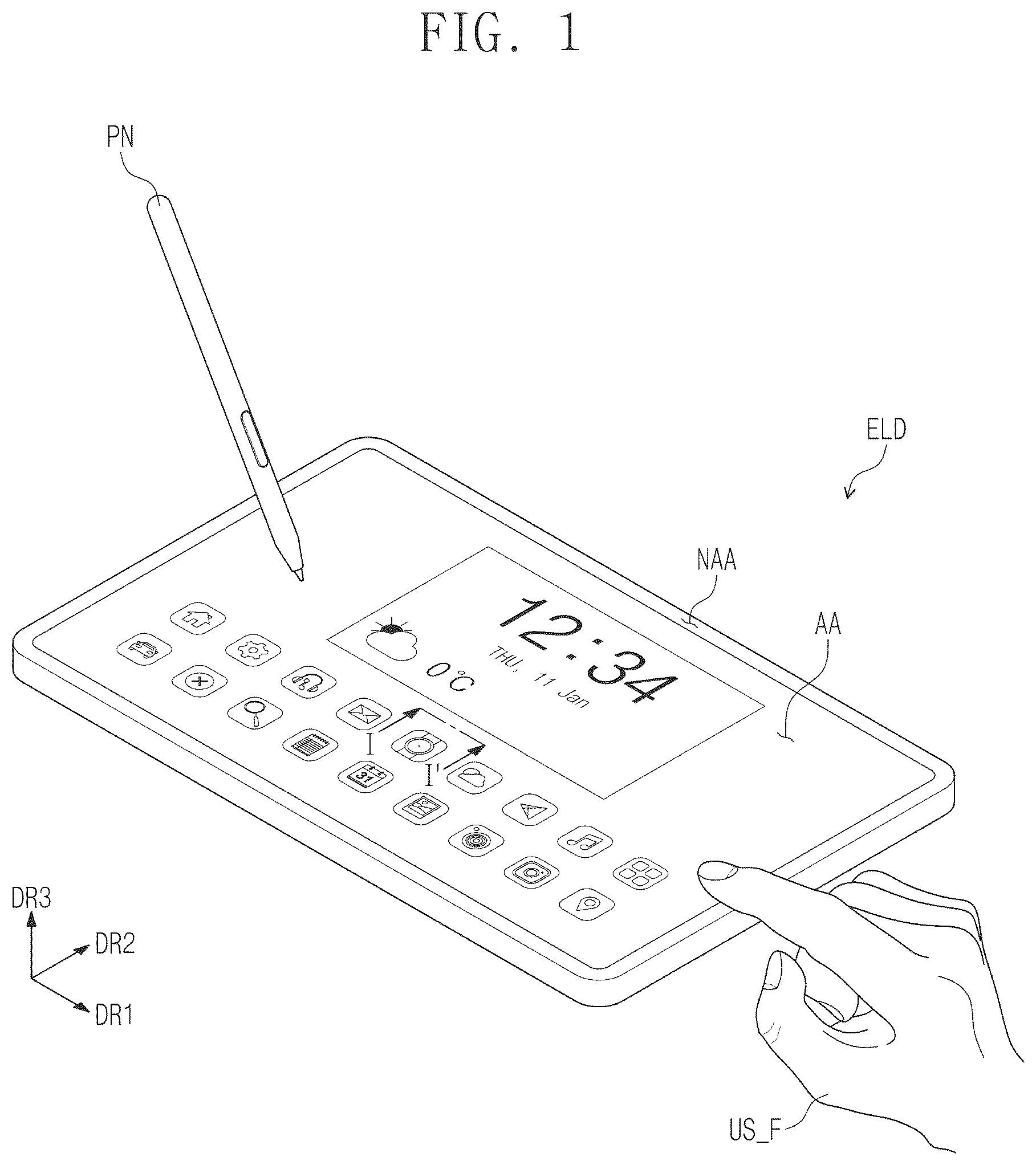
is a perspective view of an electronic device according to some embodiments of the present disclosure.
is a cross-sectional view of the electronic device according to some embodiments of the present disclosure.
is a cross-sectional view of a display module according to some embodiments of the present disclosure.
is a view for describing an operation of the electronic device according to some embodiments of the present disclosure.
is a cross-sectional view of the display module along line I-I′ of according to some embodiments of the present disclosure.
is a block diagram of a sensor layer and a sensor driving unit according to some embodiments of the present disclosure.
is a plan view of the sensor layer and the sensor driving unit according to some embodiments of the present disclosure.
is a block diagram of the sensor layer and an input detection circuit according to some embodiments of the present disclosure.
is an enlarged plan view illustrating area AA of according to some embodiments of the present disclosure.
is a cross-sectional view along line II-II′ of according to some embodiments of the present disclosure.
is a cross-sectional view along line III-III′ of according to some embodiments of the present disclosure.
is a plan view illustrating a portion of the electronic device according to some embodiments of the present disclosure.
is a view illustrating an operation of the electronic device according to some embodiments of the present disclosure.
DETAILED DESCRIPTION
In the present specification, the expression that a first component (or area, layer, part, portion, etc.) is “located on”, “connected with” or “coupled to” a second component means that the first component is directly located on/connected with/coupled to the second component or means that a third component is interposed therebetween.
The same reference numerals refer to the same components. Further, in the drawings, the thickness, the ratio, and the dimension of components are exaggerated for effective description of technical contents. The expression “and/or” includes one or more combinations which associated components are capable of defining.
Although the terms “first”, “second”, etc. may be used to describe various components, the components should not be limited by the terms. The terms are only used to distinguish one component from another component. For example, without departing from the right scope of the present disclosure, a first component may be referred to as a second component, and similarly, the second component may be also referred to as the first component. Singular expressions include plural expressions unless clearly otherwise indicated in the context.
Also, the terms “under”, “below”, “on”, “above”, etc. are used to describe the correlation of components illustrated in drawings. The terms that are relative in concept are described based on a direction illustrated in drawings.
It will be understood that the terms “include”, “comprise”, “have”, etc. specify the presence of features, numbers, steps, operations, elements, or components, described in the specification, or a combination thereof, and do not exclude in advance the presence or additional possibility of one or more other features, numbers, steps, operations, elements, or components or a combination thereof.
Unless otherwise defined, all terms (including technical terms and scientific terms) used in the specification have the same meaning as commonly understood by those skilled in the art to which the present disclosure belongs. Further, terms such as terms defined in the dictionaries commonly used should be interpreted as having a meaning consistent with the meaning in the context of the related technology and should not be interpreted in overly ideal or overly formal meanings unless explicitly defined herein.
Hereinafter, aspects of some embodiments of the present disclosure will be described with reference to the accompanying drawings.
is a perspective view of an electronic device according to some embodiments of the present disclosure.
Referring to , an electronic device ELD may be a device that is activated according to an electric signal. For example, the electronic device ELD may be a mobile phone, a foldable mobile phone, a laptop computer, a television, a tablet, a vehicle navigation system, a game console, or a wearable device, but embodiments according to the present disclosure are not limited thereto. As an example for purposes of description, illustratively illustrates that the electronic device ELD is a mobile phone.
The electronic device ELD may display images and may sense inputs applied from an external unit. The external input may be input of a user. The input of the user may include various types of external input such as a portion US_F of a body of the user, a pen PN, light, heat or a pressure. The input of the user may include all inputs that may change a capacitance of a sensor layer.
An active area AA and a peripheral area NAA may be defined in the electronic device ELD. The electronic device ELD may display images at the active area AA. The active area AA may include a plane defined by a first direction DR 1 and a second direction DR 2 . The peripheral area NAA may surround a periphery (or outside a footprint) of the active area AA. According to some embodiments of the present disclosure, the peripheral area NAA may be omitted.
A thickness direction of the electronic device ELD may be parallel to a third direction DR 3 intersecting the first direction DR 1 and the second direction DR 2 . Thus, front surfaces (or upper surfaces) and rear surfaces (or lower surfaces) of members constituting the electronic device ELD may be defined based on the third direction DR 3 .
illustratively illustrates a bar-type electronic device ELD, but embodiments according to the present disclosure are not limited thereto. For example, the following descriptions may be applied to various electronic devices ELD such as a foldable electronic device, a rollable electronic device, or a slidable electronic device.
is a cross-sectional view of the electronic device according to some embodiments of the present disclosure.
Referring to , the electronic device ELD may include a display module DM and a window WM. The display module DM may display images and detect external inputs. The display module DM may include a display layer DP and a sensor layer ISP.
A display area and a non-display area corresponding to the active area AA (see ) and the peripheral area NAA (see ) of the electronic device ELD may be defined in the display layer DP.
The display layer DP according to some embodiments of the present disclosure may be a light emitting display layer, but embodiments according to the present disclosure are not limited thereto. For example, the display layer DP may be an organic light emitting display layer, a quantum dot light emitting display layer, a micro light emitting diode (LED) display layer, or a nano LED display layer. A light emitting layer of the organic light emitting display layer may include an organic light emitting material. A light emitting layer of the quantum dot light emitting display layer may include a quantum dot, a quantum rod and the like. A light emitting layer of the micro LED display layer may include a micro LED. A light emitting layer of the nano LED display layer may include a nano LED.
The sensor layer ISP may be directly located on the display layer DP. According to some embodiments of the present disclosure, the sensor layer ISP may be formed on the display layer DP through a continuous process. That is, when the sensor layer ISP is directly located on the display layer DP, an internal adhesive layer IAL is not located between the sensor layer ISP and the display layer DP.
The electronic device ELD may further include an optical member located on the display module DM. The optical member may be a reflection preventing layer that may reduce external light reflectance. The optical member may include a polarizer and a phase retarder. The polarizer and the phase retarder may be of a stretched type or a coated type. An optical axis of the coated type optical film is defined according to a stretching direction of a functional film. The coated type optical film may include liquid crystal molecules arranged on a base film.
According to some embodiments of the present disclosure, the optical member may be omitted. In this case, the display module DM may further include a color filter and a black matrix that replace the optical member.
The window WM provides an outer surface of the electronic device ELD. The window WM may include a base substrate and may further include functional layers such as a reflection preventing layer and a fingerprint preventing layer.
According to some embodiments, the display module DM may further include at least one adhesive layer ADL. The adhesive layer ADL may couple components of the display module DM. The adhesive layer ADL may be an optical transparent adhesive layer or a pressure-sensitive adhesive layer.
The window WM may include a light shielding pattern WBM for defining the peripheral area NAA (see ). The light shielding pattern WBM may be a colored organic layer and may be formed on one surface of a window base layer WM-BS using, for example, a coating method.
is a cross-sectional view of a display module according to some embodiments of the present disclosure.
Referring to , the display module DM may include the display layer DP and the sensor layer ISP.
The display layer DP may include a base layer BL, a circuit layer DP-CL, a light emitting element layer DP-ED, and an encapsulation layer TFL.
The base layer BL may be a member that provides a base surface on which the circuit layer DP-CL is located. The base layer BL may have a multi-layer structure or a single-layer structure. The base layer BL may be a glass substrate, a metal substrate, a silicon substrate, a polymer substrate or the like, but embodiments according to the present disclosure are not limited thereto.
The circuit layer DP-CL may be located on the base layer BL. The circuit layer DP-CL may include an insulation layer, a semiconductor pattern, a conductive pattern, a signal line, and the like. The insulating layer, a semiconductor layer, and a conductive layer may be formed on the base layer BL in a manner such as coating and deposition, and the insulating layer, the semiconductor layer, and the conductive layer may be selectively patterned through a plurality of photolithography processes.
The light emitting element layer DP-ED may be located on the circuit layer DP-CL. The light emitting element layer DP-ED may include a light emitting element. For example, the light emitting element layer DP-ED may include an organic light emitting material, an inorganic light emitting material, an organic-inorganic light emitting material, a quantum dot, a quantum rod, a micro-LED, or a nano-LED.
The encapsulation layer TFL may be located on the light emitting element layer DP-ED. The encapsulation layer TFL may protect the light emitting element layer DP-ED from foreign substances or contaminants such as moisture, oxygen, and dust particles.
The sensor layer ISP may be located on the display layer DP. The sensor layer ISP may sense an external input applied from an external unit. The sensor layer ISP may be an integrated sensor formed continuously during a process of manufacturing the display layer DP or the sensor layer ISP may be an external sensor attached to the display layer DP.
is a view for describing an operation of the electronic device according to some embodiments of the present disclosure.
Referring to , the electronic device ELD may include the display layer DP, the sensor layer ISP, a display driving unit 100 C, a sensor driving unit 200 C, a main driving unit 1000 C, and a power circuit 1000 P.
The sensor layer ISP may sense first input 2000 and second input 3000 applied from an external unit. The first input 2000 and the second input 3000 may be input means that may provide a change in a capacitance of the sensor layer ISP or may be input means that may cause an induced current in the sensor layer ISP. For example, the first input 2000 may be a passive type input mechanism such as the body of the user. The second input 3000 may be an input by the pen PN or an input by a radio frequency integrated circuit (RFIC) tag. For example, the pen PN may be a passive type pan or an active type pen.
According to some embodiments of the present disclosure, the pen PN may be a device that generates a magnetic field having a resonant frequency (e.g., a set or predetermined resonant frequency). The pen PN may be configured to transmit an output signal based on an electromagnetic resonance method. The pen PN may be referred to as an input device, an input pen, a magnetic pen, a stylus pen, or an electromagnetic resonance pen.
The pen PN may include an RLC resonant circuit, and the RLC resonant circuit may include an inductor “L” and a capacitor “C.” According to some embodiments of the present disclosure, the RLC resonant circuit may be a variable resonant circuit having a variable resonant frequency. In this case, the inductor “L” may be a variable inductor and/or the capacitor “C” may be a variable capacitor, but embodiments according to the present disclosure are not limited thereto.
The inductor “L” generates a current by a magnetic field formed in the sensor layer ISP. However, embodiments according to the present disclosure are not limited thereto. For example, when the pen PN operates as an active type, the pen PN may generate a current even when the pen PN does not receive a magnetic field from an external unit. The generated current is transmitted to the capacitor “C.” The capacitor “C” charges a current input from the inductor “L” and discharges the charged current to the inductor “L.” Thereafter, the inductor “L” may emit a magnetic field having a resonant frequency. The induced current may flow in the sensor layer ISP by the magnetic field emitted by the pen PN, and the induced current as a reception signal (or a sensing signal) may be transmitted to the sensor driving unit 200 C.
The main driving unit 1000 C may control the overall operation of the electronic device ELD. For example, the main driving unit 1000 C may control operations of the display driving unit 100 C and the sensor driving unit 200 C. The main driving unit 1000 C may include at least one microprocessor and may further include a graphic controller. The main driving unit 1000 C may be referred to as an application processor, a central processing unit, or a main processor.
The display driving unit 100 C may drive the display layer DP. The display driving unit 100 C may receive image data and a control signal from the main driving unit 1000 C. The control signal may include various signals. For example, the control signal may include an input vertical synchronization signal, an input horizontal synchronization signal, a main clock, a data enable signal, and the like.
The sensor driving unit 200 C may drive the sensor layer ISP. The sensor driving unit 200 C may receive the control signal from the main driving unit 1000 C. The control signal may include a clock signal of the sensor driving unit 200 C. Further, the control signal may further include a mode determination signal that determines driving modes of the sensor driving unit 200 C and the sensor layer ISP.
The sensor driving unit 200 C may be implemented as an integrated circuit (IC) and electrically connected to the sensor layer ISP. For example, the sensor driving unit 200 C may be directly mounted on an area (e.g., a set or predetermined area) of the display layer DP or mounted on a separate printed circuit board using a chip on film (COF) method and electrically connected to the sensor layer ISP.
The sensor driving unit 200 C and the sensor layer ISP may selectively operate in a first mode or a second mode. For example, the first mode may be a mode for sensing a touch input, for example, the first input 2000 . The second mode may be a mode for sensing the input by the pen PN, for example, the second input 3000 . The first mode may be referred to as a touch sensing mode, and the second mode may be referred to as a pen sensing mode.
Switching between the first mode and the second mode may be performed in various manners. For example, the sensor driving unit 200 C and the sensor layer ISP may be driven in the first mode and the second mode in a time division manner and may sense the first input 2000 and the second input 3000 . Alternatively, the switching between the first mode and the second mode may be generated by selection by the user or by a specific action of the user, any one of the first mode and the second mode may be activated or deactivated by activating or deactivating a specific application, or a current mode may be switched from one to the other one of the first mode and the second mode. Alternatively, while the sensor driving unit 200 C and the sensor layer ISP are operating alternately in the first mode and the second mode, when the first input 2000 is sensed, the first mode is maintained or when the second input 3000 is sensed, the second mode is maintained.
The sensor driving unit 200 C may calculate coordinate information of input based on a signal received from the sensor layer ISP and provide a coordinate signal having the coordinate information to the main driving unit 1000 C. The main driving unit 1000 C executes an operation corresponding to the input of the user based on the coordinate signal. For example, the main driving unit 1000 C may operate the display driving unit 100 C so that a new application image is displayed on the display layer DP.
The power circuit 1000 P may include a power management integrated circuit (PMIC). The power circuit 1000 P may generate a plurality of driving voltages for driving the display layer DP, the sensor layer ISP, the display driving unit 100 C, and the sensor driving unit 200 C. For example, the plurality of driving voltages may include a first driving voltage (e.g., an ELVSS voltage), a second driving voltage (e.g., an ELVDD voltage), an initialization voltage or the like, but embodiments according to the present disclosure are not limited to the above example.
is a cross-sectional view of the display module along the line I-I′ of according to some embodiments of the present disclosure. In the description of , the components described through are designated by the same reference numerals, and some repetitive description thereof may be omitted.
Referring to , the base layer BL may provide a base surface on which the circuit layer DP-CL is located. The circuit layer DP-CL may be located on the base layer BL. The circuit layer DP-CL may include an insulation layer, a semiconductor pattern, a conductive pattern, a signal line, and the like. The insulating layer, the semiconductor layer, and the conductive layer may be formed on the base layer BL in a manner such as coating and deposition, and then the insulating layer, the semiconductor layer, and the conductive layer may be selectively patterned through a plurality of photolithography processes. Thereafter, the semiconductor pattern, the conductive pattern, and the signal line included in the circuit layer DP-CL may be formed.
At least one inorganic layer is formed on an upper surface of the base layer BL. According to some embodiments, it is illustrated that the display layer DP includes a buffer layer BFL. The buffer layer BFL may relatively improve a coupling force between the base layer BL and the semiconductor pattern. The buffer layer BFL may include a silicon oxide layer and a silicon nitride layer, and the silicon oxide layer and the silicon nitride layer may be alternately laminated.
The semiconductor pattern may be located on the buffer layer BFL. The semiconductor pattern may include polysilicon. However, embodiments according to the present disclosure are not limited thereto, and the semiconductor pattern may include amorphous silicon or metal oxide.
merely illustrates a portion of the semiconductor pattern, and the semiconductor pattern may be further located in another area. The semiconductor pattern may be located in a specific rule across pixels. The semiconductor pattern may have a different electrical property depending on whether or not the semiconductor pattern is doped. The semiconductor pattern may include a first area having higher conductivity and a second area having lower conductivity. The first area may be doped with an N-type dopant or a P-type dopant. A P-type transistor includes a doped area doped with the P-type dopant. The second area may be a non-doped area or may be doped at a concentration lower than that of the first area.
A conductivity of the first area is greater than a conductivity of the second area, and the first area substantially serves as an electrode or a signal line. The second area may substantially correspond to an active area (or a channel area) of a pixel transistor TR-P. In other words, a portion of the semiconductor pattern may be the active area of the transistor, and the other portion thereof may be a source area or a drain area of the transistor.
Each of pixels may have an equivalent circuit including seven transistors, one capacitor, and a light emitting element, and the equivalent circuit of the pixel may be modified into various forms. illustratively illustrates one pixel transistor TR-P and one light emitting element ED included in the pixel.
A source area SR, a channel area CHR, and a drain area DR of the pixel transistor TR-P may be formed from the semiconductor pattern. The source area SR and the drain area DR may extend from the channel area CHR in opposite directions on a cross section. illustrates a portion of a signal transmitting area SCL formed in the first area of the semiconductor pattern. According to some embodiments, the signal transmitting area SCL may be electrically connected to the pixel transistor TR-P on a plane.
A first insulating layer IL 1 may be located on the buffer layer BFL. The first insulating layer IL 1 may commonly overlap the plurality of pixels and cover the semiconductor pattern. The first insulating layer IL 1 may be an inorganic layer and/or an organic layer and may have a single-layer structure or a multi-layer structure. The first insulating layer IL 1 may include at least one of an aluminum oxide, a titanium oxide, a silicon oxide, a silicon nitride, a silicon oxy nitride, a zirconium oxide, or a hafnium oxide. According to some embodiments, the first insulating layer IL 1 may be a single-layered silicon oxide layer. An insulating layer of the circuit layer DP-CL, which will be described below, as well as the first insulating layer IL 1 may be an inorganic layer and/or an organic layer and may have a single-layer structure or a multi-layer structure. The inorganic layer may include at least one of the above-described materials, but embodiments according to the present disclosure are not limited thereto.
A gate GE of the pixel transistor TR-P is located on the first insulating layer IL 1 . The gate GE may be a portion of a metal pattern. The gate GE overlaps the channel area CHR. The gate GE may function as a mask in a process of doping the semiconductor pattern.
A second insulating layer IL 2 may be located on the first insulating layer IL 1 and cover the gate GE. The second insulating layer IL 2 may commonly overlap the pixels. The second insulating layer IL 2 may be an inorganic layer and/or an organic layer and may have a single-layer structure or a multi-layer structure. According to some embodiments, the second insulating layer IL 2 may be a single-layered silicon oxide layer.
A third insulating layer IL 3 may be located on the second insulating layer IL 2 , and according to some embodiments, the third insulating layer IL 3 may be a single-layer silicon oxide layer. A first connection electrode CNE 1 may be located on the third insulating layer IL 3 . The first connection electrode CNE 1 may be connected to the signal transmitting area SCL through a contact hole CNT 1 passing through the first insulating layer IL 1 , the second insulating layer IL 2 , and the third insulating layer IL 3 .
A fourth insulating layer IL 4 may be located on the third insulating layer IL 3 . The fourth insulating layer IL 4 may be a single-layer silicon oxide layer. A fifth insulating layer IL 5 may be located on the fourth insulating layer IL 4 . The fifth insulating layer IL 5 may be an organic layer. Meanwhile, the fourth insulating layer IL 4 may be omitted, and the fifth insulating layer IL 5 may be located on the third insulating layer IL 3 .
A second connection electrode CNE 2 may be located on the fifth insulating layer IL 5 . The second connection electrode CNE 2 may be connected to the first connection electrode CNE 1 through a contact hole CNT 2 passing through the fourth insulating layer IL 4 and the fifth insulating layer IL 5 .
A sixth insulating layer IL 6 may be located on the fifth insulating layer IL 5 and cover the second connection electrode CNE 2 . The sixth insulating layer IL 6 may be an organic layer. The light emitting element layer DP-ED may be located on the circuit layer DP-CL. The light emitting element layer DP-ED may include the light emitting element ED. The light emitting element ED may include a first electrode AE, a light emitting layer EL, and a second electrode CE. For example, the light emitting layer EL may include an organic light emitting material, a quantum dot, a quantum rod, a micro LED, or a nano LED.
The first electrode AE may be located on the sixth insulating layer IL 6 . The first electrode AE may be connected to the second connection electrode CNE 2 through a contact hole CNT 3 passing through the sixth insulating layer IL 6 .
A pixel defining film IL 7 may be located on the sixth insulating layer IL 6 and cover a portion of the first electrode AE. An opening OP 7 is defined in the pixel defining film IL 7 . At least a portion of the first electrode AE is exposed through the opening OP 7 of the pixel defining film IL 7 . According to some embodiments, a light emitting area PXA is defined to correspond to a partial area of the first electrode AE, which is exposed by the opening OP 7 . A non-light emitting area NPXA may surround the light emitting area PXA.
The light emitting layer EL may be located on the first electrode AE. The light emitting layer EL may be arranged to correspond to the opening OP 7 . That is, the light emitting layers EL may be formed separately from the respective pixels. When the light emitting layers EL are formed separately from the respective pixels, each of the light emitting layers EL may emit a light having at least one of a blue color, a red color, or a green color. However, embodiments according to the present disclosure are not limited thereto, and the light emitting layers EL may be connected to the pixels and may be provided commonly. In this case, the light emitting layer EL may also provide a blue light or a white light.
The second electrode CE may be located on the light emitting layer EL. The second electrode CE may have an integral shape and may be arranged in the plurality of pixels in common. A common voltage may be provided to the second electrode CE and the second electrode CE may be referred to as a common electrode.
According to some embodiments, a hole control layer may be located between the first electrode AE and the light emitting layer EL. The hole control layer may be commonly located in the light emitting area PXA and the non-light emitting area NPXA. The hole control layer may include a hole transport layer and may further include a hole injection layer. An electron control layer may be located between the light emitting layer EL and the second electrode CE. The electron control layer may include an electron transport layer and may further include an electron injection layer. The hole control layer and the electron control layer may be commonly formed in the pixels using an open mask.
The sensor layer ISP may be directly formed on an upper surface of the encapsulation layer TFL through a continuous process. The sensor layer ISP may include a first sensor insulating layer IIL 1 , a first sensor conductive layer ICL 1 , a second sensor insulating layer IIL 2 , a second sensor conductive layer ICL 2 , and a third sensor insulating layer IIL 3 . In the specification, the first sensor insulating layer IIL 1 may be referred to as a “base insulating layer.”
Each of the first sensor conductive layer ICL 1 and the second sensor conductive layer ICL 2 may include a plurality of patterns having a single-layer structure or having a multi-layer structure in which layers are laminated in the third direction DR 3 . The conductive layer having the single-layer structure may include a metal layer or a transparent conductive layer. The metal layer may include molybdenum, silver, titanium, copper, aluminum, or alloys thereof. The transparent conductive layer may include a transparent conductive oxide such as an indium tin oxide (ITO), an indium a zinc oxide (IZO), a zinc oxide (ZnO), an indium zinc tin oxide (IZTO). In addition, the transparent conductive layer may include a conductive polymer such as poly(3,4-ethylenedioxythiophene) (PEDOT), metal nanowire, graphene, or the like.
The conductive layer having a multi-layer structure may include metal layers. The metal layers may have, for example, a three-layer structure of titanium/aluminum/titanium. The conductive layer having the multi-layer structure may include at least one metal layer and at least one transparent conductive layer.
The second sensor insulating layer IIL 2 covers the first sensor conductive layer ICL 1 , and the third sensor insulating layer IIL 3 covers the second sensor conductive layer ICL 2 . It is illustrated that the first sensor insulating layer IIL 1 to the third sensor insulating layer IIL 3 have the single-layer structures, but embodiments according to the present disclosure are not limited thereto.
At least one of the first sensor insulating layer IIL 1 or the second sensor insulating layer IIL 2 may include an inorganic layer. The inorganic film may include at least one of an aluminum oxide, a titanium oxide, a silicon oxide, a silicon nitride, a silicon oxy nitride, a zirconium oxide, or a hafnium oxide.
At least one of the second sensor insulating layer IIL 2 or the third sensor insulating layer IIL 3 may include an organic layer. The organic film may include at least one of an acryl-based resin, a methacrylate-based resin, a polyisoprene-based resin, a vinyl-based resin, an epoxy-based resin, a urethane-based resin, a cellulose-based resin, a siloxane-based resin, a polyimide-based resin, a polyamide-based resin, or a perylene-based resin.
is a block diagram of a sensor layer and a sensor driving unit according to some embodiments of the present disclosure.
Referring to , an active area SA and a peripheral area NSA adjacent to the active area SA may be defined in the sensor layer ISP. The active area SA and the peripheral area NSA may correspond to the active area AA (see ) and the peripheral area NAA (see ) of the electronic device ELD (see ), respectively. The active area SA may be an area that is activated according to an electric signal. For example, the active area SA may be an area that senses an input.
The sensor layer ISP may include a plurality of first electrodes RE and a plurality of second electrodes TE.
The plurality of first electrodes RE may be arranged to be spaced apart from each other in the second direction DR 2 . The plurality of first electrodes RE may extend in the first direction DR 1 .
The plurality of second electrodes TE may be arranged to be spaced apart from each other in the first direction DR 1 . The plurality of second electrodes TE may extend in the second direction DR 2 .
The sensor driving unit 200 C may be electrically connected to the sensor layer ISP. The sensor driving unit 200 C may control the sensor layer ISP. The sensor driving unit 200 C may receive a control signal I-CS from the main driving unit 1000 C (see ) and provide a coordinate signal I-SS to the main driving unit 1000 C (see ).
The sensor driving unit 200 C may include a sensor controlling circuit 200 C 1 , a signal generating circuit 200 C 2 , and an input detecting circuit 200 C 3 . The sensor controlling circuit 200 C 1 , the signal generating circuit 200 C 2 , and the input detecting circuit 200 C 3 may be implemented in a single chip or some and the others of the sensor controlling circuit 200 C 1 , the signal generating circuit 200 C 2 , and the input detecting circuit 200 C 3 may be implemented within different chips.
The sensor controlling circuit 200 C 1 may control a mode of the sensor layer ISP. The sensor controlling circuit 200 C 1 may control an operation of the signal generating circuit 200 C 2 and calculate coordinates of an external input from a signal received from the input detecting circuit 200 C 3 .
The signal generating circuit 200 C 2 may output an output signal corresponding to an operation mode to the sensor layer ISP. The signal generating circuit 200 C 2 may provide a first touch signal TS (or a driving signal), which is referred to as a TX signal, to the sensor layer ISP. The first touch signal TS may be sequentially provided to the plurality of second electrodes TE.
The input detecting circuit 200 C 3 may convert an analog signal, which is a second touch signal RS (or a detecting signal) referred to as an RX signal received from the sensor layer ISP, into a digital signal. The input detecting circuit 200 C 3 may amplify and then filter the received analog signal. Thereafter, the input detecting circuit 200 C 3 may convert the filtered signal into the digital signal. The input detecting circuit 200 C 3 may reduce or remove noise of the received second touch signal RS. This will be described below.
is a plan view of the sensor layer and the sensor driving unit according to some embodiments of the present disclosure. In the description of , the components described through are designated by the same reference numerals, and some repetitive description thereof may be omitted.
Referring to , an active area SA and a peripheral area NSA may be defined in the sensor layer ISP. A portion of the active area may be defined as a first area AR 1 , and the other portion of the active area SA may be defined as a second area AR 2 . That is, when viewed on a plane (e.g., in a plan view), the first area AR 1 and the second area AR 2 may not overlap each other. The second area AR 2 may be adjacent to the first area AR 1 in the first direction DR 1 .
The sensor layer ISP may include the plurality of first electrodes RE, the plurality of second electrodes TE, a first line L 1 , a second line L 2 , a third line L 3 , a fourth line L 4 , and a fifth line L 5 .
The plurality of first electrodes RE and the plurality of second electrodes TE may be electrically insulated from each other and may intersect each other.
Each of the plurality of first electrodes RE may include a plurality of first sub-electrodes SME 1 and a plurality of second sub-electrodes SME 2 . The plurality of first sub-electrodes SME 1 and the plurality of second sub-electrodes SME 2 may be alternately arranged in the first direction DR 1 . The plurality of first sub-electrodes SME 1 and the plurality of second sub-electrodes SME 2 may be electrically insulated from each other.
According to the present disclosure, a first channel including the plurality of first sub-electrodes SME 1 and a second channel including the plurality of second sub-electrodes SME 2 may be defined in each of the plurality of first electrodes RE. The number of channels of the plurality of first electrodes RE that receive the second touch signal RS (see ) may increase, and accordingly, noise may be reduced by half. Accordingly, the electronic device ELD (see ) having relatively improved sensing reliability may be provided.
The plurality of first electrodes RE may include a first row first electrode RE 1 , a second row first electrode RE 2 , a (k−1) th row first electrode REk−1, and a k th row first electrode REk. In this case, k may be a natural number greater than 3. The first row first electrode RE 1 , the second row first electrode RE 2 , the (k−1) th row first electrode REk−1, and the k th row first electrode REk may be arranged in the second direction DR 2 .
The plurality of second electrodes TE may include a first column second electrode TE 1 , a second column second electrode TE 2 , a (n−1) th column second electrode TEn−1, and a n th column second electrode TEn. In this case, n may be a natural number greater than 3. The first column second electrode TE 1 , the second column second electrode TE 2 , the (n−1) th column second electrode TEn−1, and the n th column second electrode TEn may be arranged in the first direction DR 1 .
The first line L 1 may be electrically connected to a plurality of first sub-electrodes SME 1 . The first line L 1 located in the active area SA may extend in the first direction DR 1 , and the first line L 1 located in the peripheral area NSA may extend in the second direction DR 2 .
The plurality of first sub-electrodes SME 1 may be electrically connected to the sensor driving unit 200 C through the first line L 1 .
The second line L 2 may be electrically connected to the plurality of second sub-electrodes SME 2 . The second line L 2 located in the active area SA may extend in the first direction DR 1 , and the second line L 2 located in the peripheral area NSA may extend in the second direction DR 2 . Within the active area SA, the second line L 2 may be spaced apart from the first line L 1 in the second direction DR 2 .
The third line L 3 may be connected to one of the plurality of first sub-electrodes SME 1 . The third line L 3 may extend in the second direction DR 2 . The third line L 3 may be located in the first area AR 1 . When viewed on a plane (e.g., in a plan view), the third line L 3 may not overlap the second area AR 2 . The third line L 3 may be provided as a plurality of third lines L 3 , and the plurality of third lines L 3 may be electrically connected to the plurality of first electrodes RE, respectively. In a plan view, the third line L 3 may overlap one of the plurality of second electrodes TE.
The fourth line L 4 may be connected to one of the plurality of second sub-electrodes SME 2 . The fourth line L 4 may extend in the second direction DR 2 . The fourth line L 4 may be located in the second area AR 2 . When viewed on a plane (e.g., in a plan view), the fourth line L 4 may not overlap the first area AR 1 . The fourth line L 4 may be provided as a plurality of fourth lines L 4 , and the plurality of fourth lines L 4 may be electrically connected to the plurality of first electrodes RE, respectively. In a plan view, the fourth line L 4 may overlap one of the plurality of second electrodes TE.
According to the present disclosure, the third line L 3 and the fourth line L 4 may extend to overlap the active area SA. For example, the third line L 3 and the fourth line L 4 may not be arranged in the peripheral area NSA adjacent to the active area SA in the first direction DR 1 . An area of the peripheral area NSA may be reduced. Thus, an area of the peripheral area NAA (see ) may be reduced, and the electronic device ELD (see ) in which a narrow bezel is implemented may be provided.
The first to fourth lines L 1 to L 4 may be electrically connected to the sensor driving unit 200 C. The first to fourth lines L 1 to L 4 may transmit the second touch signal RS (see ) to the sensor driving unit 200 C.
According to the present disclosure, four wiring lines including the first to fourth lines L 1 to L 4 may be connected to one first electrode RE. A resistance of the wiring line that transmits the second touch signal RS (see ) may be reduced. Accordingly, a bandwidth of the wiring line may increase. A range of a selectable frequency increases, and thus noise may be more easily avoided, and touch performance may be relatively improved. Accordingly, the electronic device ELD (see ) having relatively improved sensing reliability may be provided.
The fifth line L 5 may be provided as a plurality of fifth lines L 5 . The plurality of fifth lines L 5 may be connected to the plurality of second electrodes TE, respectively. The plurality of fifth lines L 5 may be arranged in the peripheral area NSA.
The plurality of fifth lines L 5 may be electrically connected to the sensor driving unit 200 C. The plurality of fifth lines L 5 may sequentially provide the first touch signal TS (see ) to the plurality of second electrodes TE.
The sensor driving unit 200 C may acquire information on the input of the user based on a change in a mutual capacitance between the plurality of first electrodes RE and the plurality of second electrodes TE.
The change in the mutual capacitance between the plurality of second electrodes TE and the plurality of first electrodes RE may occur at a position in which the input of the user is provided. The sensor driving unit 200 C may generate coordinate values for the position in which the input of the user is provided, based on the reception signals received from the first to fourth lines L 1 to L 4 .
is a block diagram of the sensor layer and an input detection circuit according to some embodiments of the present disclosure.
Referring to , the input detecting circuit 200 C 3 may include a differential amplifier DAMP. The first line L 1 may be electrically connected to a first terminal (e.g., a negative terminal) of the differential amplifier DAMP, and the second line L 2 may be electrically connected to a second terminal (e.g., a positive terminal) thereof.
The second touch signal RS input to the first terminal is referred to as a first reception signal, and the second touch signal RS input to the second terminal is referred to as a second reception signal. The differential amplifier DAMP may generate a difference between the first reception signal and the second reception signal as an output signal. That is, the sensor driving unit 200 C may acquire touch information in the active area SA using the difference between the first reception signal and the second reception signal.
is an enlarged plan view illustrating area AA of according to some embodiments of the present disclosure, is a cross-sectional view along line II-II′ of according to some embodiments of the present disclosure, and is a cross-sectional view along line III-III′ of according to some embodiments of the present disclosure. In the description of , the components described through are designated by the same reference numerals, and some repetitive description thereof may be omitted.
Referring to to 11 , open parts T_OP 1 and T_OP 2 extending in the second direction DR 2 may be defined in the plurality of second electrodes TE. illustratively illustrates the first open part T_OP 1 defined in the first column second electrode TE 1 and the second open part T_OP 2 defined in the second column second electrode TE 2 .
A boundary open part T_BOP may be defined between two adjacent second electrodes TE among the plurality of second electrodes TE.
A corresponding first sub-electrode SME 1 among the plurality of first sub-electrodes SME 1 may be arranged to correspond to the first open part T_OP 1 and the boundary open part T_BOP. The plurality of first sub-electrodes SME 1 may include a plurality of first segment electrodes S_SME 1 and a plurality of first bridge electrodes SBE 1 .
Each of the plurality of first segment electrodes S_SME 1 may have a quadrangular shape including two horizontal sides parallel to the first direction DR 1 and two vertical sides parallel to the second direction DR 2 . The plurality of first segment electrodes S_SME 1 may be spaced apart from each other in the first direction DR 1 and the second direction DR 2 . The plurality of first bridge electrodes SBE 1 may be connected to the plurality of first segment electrodes S_SME 1 .
The plurality of first sub-electrodes SME 1 may be electrically connected to the first line L 1 through a first contact hole CCH 1 . The first line L 1 may extend in the first direction DR 1 .
A corresponding second sub-electrode SME 2 among the plurality of second sub-electrodes SME 2 may be arranged to correspond to the second open part T_OP 2 and the boundary open part T_BOP. The plurality of second sub-electrodes SME 2 may include a plurality of second segment electrodes S_SME 2 and a plurality of second bridge electrodes SBE 2 .
Each of the plurality of second segment electrodes S_SME 2 may have a quadrangular shape including two horizontal sides parallel to the first direction DR 1 and two vertical sides parallel to the second direction DR 2 . The plurality of second segment electrodes S_SME 2 may be spaced apart from each other in the first direction DR 1 and the second direction DR 2 . The plurality of second bridge electrodes SBE 2 may be connected to the plurality of second segment electrodes S_SME 2 .
The plurality of second sub-electrodes SME 2 may be electrically connected to the second line L 2 through a second contact hole CCH 2 . The second line L 2 may extend in the first direction DR 1 .
The first line L 1 and the second line L 2 may be spaced apart from each other in the second direction DR 2 with the plurality of first sub-electrodes SME 1 and the plurality of second sub-electrodes SME 2 interposed therebetween.
The third line L 3 may be connected to one of the plurality of first sub-electrodes SME 1 . The third line L 3 may extend in the second direction DR 2 . The third line L 3 may be located on the first sensor insulating layer IIL 1 . The second sensor insulating layer IIL 2 may cover the third line L 3 . The plurality of first segment electrodes S_SME 1 may be arranged on the second sensor insulating layer IIL 2 . The third line L 3 may be electrically connected to the plurality of first segment electrodes S_SME 1 through a segment contact hole SCH 1 . The third line L 3 and the plurality of first segment electrodes S_SME 1 may have a mesh structure.
The third line L 3 may include a first part SLP 1 and a second part SLP 2 . The first part SLP 1 , the second part SLP 2 , the first line L 1 , and the second line L 2 may be arranged on the first sensor insulating layer IIL 1 . The first part SLP 1 may be provided as a plurality of first parts SLP 1 . The first line L 1 and the second line L 2 may be arranged between the plurality of first parts SLP 1 .
The second sensor insulating layer IIL 2 may cover the plurality of first parts SLP 1 , the first line L 1 , and the second line L 2 . The second part SLP 2 may be located on the second sensor insulating layer IIL 2 . The second part SLP 2 may be electrically connected to the plurality of first parts SLP 1 through a plurality of line contact holes BCNT 1 and BCNT 2 .
When viewed on a plane (e.g., in a plan view), the second part SLP 2 may overlap the first line L 1 and the second line L 2 .
illustratively illustrates the plurality of first electrodes RE and the plurality of second electrodes TE having a bar stripe shape, but the shapes of the plurality of first electrodes RE and the plurality of second electrodes TE according to some embodiments of the present disclosure are not limited thereto. For example, the plurality of first electrodes RE and the plurality of second electrodes TE may have a diamond pattern shape.
is a plan view illustrating a portion of the electronic device according to some embodiments of the present disclosure, and is a view illustrating an operation of the electronic device according to some embodiments of the present disclosure. In the description of , the components described through are designated by the same reference numerals, and some repetitive description thereof may be omitted.
Referring to , when the user uses the pen PN, the user may use the pen PN while an arm of the user is seated on the active area SA. In this case, the arm may act as a large-area conductor TC, extend in the same direction as that of the third line L 3 or the fourth line L 4 , and generate a coupling capacitor C_TC. For example, when the third line L 3 directly connected to the first sub-electrode SME 1 located on a leftmost side among the plurality of first sub-electrodes SME 1 of the first row first electrode RE 1 overlaps the large-area conductor TC on a plane, a capacitance of the coupling capacitor C_TC of a node corresponding to the first sub-electrode SME 1 may increase.
When viewed on a plane (e.g., in a plan view), and when the large-area conductor TC overlaps the third line L 3 located in the first area AR 1 , the large-area conductor TC may not overlap the second area AR 2 spaced apart from the first area AR 1 in the first direction DR 1 . Accordingly, the large-area conductor TC may not overlap the fourth line L 4 on a plane. That is, when one of the third line L 3 and the fourth line L 4 overlaps the large-area conductor TC, the other one of the third line L 3 and the fourth line L 4 may not overlap the large-area conductor TC.
The third line L 3 and the fourth line L 4 connected to the plurality of first electrodes RE may be spaced apart from each other in the first direction DR 1 with at least one of the plurality of first sub-electrodes SME 1 or at least one of the plurality of second sub-electrodes SME 2 interposed therebetween. That is, the third line L 3 may be located in the first area AR 1 , and the fourth line L 4 may be located on the second area AR 2 spaced apart from the first area AR 1 in the first direction DR 1 .
The third line L 3 may be expressed as a first resistor R_L 3 and a first capacitor C_L 3 .
When the coupling capacitor C_TC is formed on the third line L 3 by the large-area conductor TC, the fourth line L 4 may be spaced a distance (e.g., a set or predetermined distance) from the third line L 3 in the first direction DR 1 and thus may not overlap the large-area conductor TC. That is, the fourth line L 4 may be spatially separated from the large-area conductor TC. Accordingly, a coupling capacitor may not be formed in the fourth line L 4 .
The fourth line L 4 may be expressed as a second resistor R_L 4 and a second capacitor C_L 4 .
The third line L 3 and the fourth line L 4 may be connected to the sensor driving unit 200 C through a pad part PAD. The sensor driving unit 200 C may include the input detecting circuit 200 C 3 .
The input detecting circuit 200 C 3 may include a plurality of signal receiving units 201 C 3 , a plurality of conversion circuits 202 C 3 , and a signal processing unit 203 C 3 .
The plurality of signal receiving units 201 C 3 may amplify and output the received signal. The plurality of signal receiving units 201 C 3 may be connected to the pad part PAD. That is, the third line L 3 may be electrically connected to one of the plurality of signal receiving units 201 C 3 , and the fourth line L 4 may be electrically connected to the other one of the plurality of signal receiving units 201 C 3 .
The plurality of signal receiving units 201 C 3 may output a signal corresponding to a voltage difference between the first terminal and the second terminal through an output terminal. Each of the plurality of signal receiving units 201 C 3 may be implemented as an analog front end (AFE) including an amplifier AMP, the capacitor “C,” and a switch SW. The amplifier AMP may include an operational (OP) amplifier.
A first terminal of the amplifier AMP may be electrically connected to the pad part PAD. A reference voltage Vref may be provided to a second terminal of the amplifier AMP.
The capacitor “C” and the switch SW may be connected in parallel between the first terminal of the amplifier AMP and the output terminal.
The plurality of conversion circuits 202 C 3 may convert analog signals input from the plurality of signal receiving units 201 C 3 into digital signals. Each of the plurality of conversion circuits 202 C 3 may include an analog-digital converter ADC.
The signal processing unit 203 C 3 may process the converted signal (digital signal) from the plurality of conversion circuits 202 C 3 and compensate for a ghost touch based on the signal processing result.
A first sensing signal sensed by the third line L 3 may include noise due to the large-area conductor TC. In this case, a second sensing signal sensed by the fourth line L 4 may be a signal that does not include noise.
The signal processing unit 203 C 3 may calculate a difference between the first sensing signal and the second sensing signal that are converted into digital signals. The signal processing unit 203 C 3 may compensate for coordinates based on the difference.
The sensor driving unit 200 C may compensate for the coordinates based on the difference between the first sensing signal sensed by the third line L 3 and the second sensing signal sensed by the fourth line L 4 . Malfunction such as a ghost touch caused by the large-area conductor TC may be prevented or reduced.
According to the present disclosure, when the large-area conductor TC overlaps any one of the third line L 3 and the fourth line L 4 and thus the coupling capacitor C_TC is formed at a specific node, the other one of the third line L 3 and the fourth line L 4 may not overlap the large-area conductor TC. The signal processing unit 203 C 3 may receive the first sensing signal obtained by converting a signal in which noise is generated by the coupling capacitor C_TC into the digital signal and the second sensing signal obtained by converting a signal in which the noise is not generated into the digital signal. The signal processing unit 203 C 3 may extract only a noise signal corresponding to the noise based on the difference between the first sensing signal and the second sensing signal. The signal processing unit 203 C 3 may compensate for the coordinates based on the noise signal. Accordingly, the electronic device ELD (see ) having relatively improved sensing reliability may be provided.
According to the above description, when a large-area conductor overlaps any one of the third line and the fourth line so that a coupling capacitor is formed at a specific node, the other one of the third line and the fourth line may not overlap the large-area conductor. A sensor driving unit may receive a first sensing signal obtained by converting a signal in which noise is generated by the coupling capacitor into a digital signal and a second sensing signal obtained by converting a signal in which no noise is generated into a digital signal. The sensor driving unit may extract only a noise signal corresponding to the noise based on a difference between the first sensing signal and the second sensing signal. The sensor driving unit may compensate for coordinates based on the noise signal. Thus, an electronic device having relatively improved sensing reliability may be provided.
Although the description has been made above with reference to aspects of some embodiments of the present disclosure, it may be understood that those skilled in the art or those having ordinary knowledge in the art may variously modify and change the present disclosure without departing from the spirit and technical scope of the present disclosure described in the appended claims, and their equivalents. Thus, the technical scope of the present disclosure is not limited to the detailed description of the specification, but should be defined by the appended claims, and their equivalents.
Figures (11)
Citations
This patent cites (17)
- US9081453
- US9898146
- US10775942
- US10969907
- US11531438
- US11567617
- US11573663
- US11789561
- US11847283
- US11861112
- US2011/0234523
- US2013/0181943
- US2015/0261348
- US2018/0373359
- US2021/0382580
- US2022/0276761
- US2024/0118769