Display Device Including a Touch Electrode
Abstract
A display device includes a substrate; a plurality of light emitting units disposed on the substrate; a plurality of light sensing units disposed on the substrate; a pixel defining layer partitioning the plurality of light emitting units and the plurality of light sensing units; and a touch electrode disposed on the pixel defining layer. A shape of a mesh hole defined by the touch electrode and in which the plurality of light sensing units are disposed is defined by the touch electrode, and is different from a shape of a mesh hole in which a first light emitting unit among the plurality of light emitting units is disposed.
Claims (21)
1 . A display device, comprising: a substrate; a plurality of light emitting units disposed on the substrate; a plurality of light sensing units disposed on the substrate; a pixel defining layer partitioning the plurality of light emitting units and the plurality of light sensing units; and a touch electrode disposed on the pixel defining layer, wherein a shape of a mesh hole defined by the touch electrode and in which the plurality of light sensing units are disposed is defined by the touch electrode, and is different from a shape of a mesh hole in which a particular light emitting unit among the plurality of light emitting units is disposed, wherein a first distance between any one of the plurality of light sensing units and the touch electrode in one direction is equal to a second distance between the touch electrode and the particular light emitting unit, of the plurality of light emitting units, adjacent to the light sensing unit in the one direction, wherein the mesh hole in which each of the plurality of light sensing units is disposed has a rectangular planar shape, and the mesh hole in which each the plurality of light emitting units is disposed has a hexagonal planar shape, wherein the rectangular mesh hole of each of the plurality of light sensing units is surrounded on four sides thereof by four hexagonal mesh holes of four light emitting units of the plurality of light emitting units that are closest thereto, and wherein the rectangular mesh hole of the plurality of light sensing units combines with the hexagonal mesh holes of the four light emitting units to form an octagonal pixel unit in which the rectangular mesh hole of the plurality of light sensing units is at a center of.
8 . A display device, comprising: a substrate; a plurality of light emitting units disposed on the substrate; a plurality of light sensing units disposed on the substrate; a pixel defining layer partitioning the plurality of light emitting units and the plurality of light sensing units; and a touch electrode disposed on the pixel defining layer, wherein the touch electrode comprises first electrode lines extending in a first direction, second electrode lines extending in a second direction intersecting the first direction, third electrode lines extending in a first diagonal direction inclined with respect to the first direction, and fourth electrode lines extending in a second diagonal direction intersecting the first diagonal direction, wherein a first distance between any one of the plurality of light sensing units and the touch electrode in one direction is equal to a second distance between the touch electrode and a particular light emitting unit, of the plurality of light emitting units, adjacent to the light sensing unit in the one direction, wherein the touch electrode defines rectangular mesh holes surrounding each of the plurality of light emitting units and hexagonal mesh holes surrounding each of the plurality of light sensing units, wherein the rectangular mesh hole of each of the plurality of light sensing units is surrounded on four sides thereof by four hexagonal mesh holes of four light emitting units of the plurality of light emitting units that are closest thereto, and wherein the rectangular mesh hole of the plurality of light sensing units combines with the hexagonal mesh holes of the four light emitting units to form an octagonal pixel unit in which the rectangular mesh hole of the plurality of light sensing units is at a center of.
17 . An electronic device, comprising: a substrate; a plurality of light emitting units disposed on the substrate; a plurality of light sensing units disposed on the substrate; a pixel defining layer partitioning the plurality of light emitting units and the plurality of light sensing units; and a plurality of first sensor portions disposed on the pixel defining layer and extending in one direction and a contact area connecting the plurality of first sensor portions, wherein the plurality of first sensor portions comprise a first electrode line disposed outside any one of the plurality of light sensing units and a second electrode line intersecting the first electrode line, wherein the contact area is not disposed on either the first electrode line or the second electrode line, wherein a first distance between any one of the plurality of light sensing units and the first sensor portions in one direction is equal to a second distance between the first sensor portions and a particular light emitting unit, of the plurality of light emitting units, adjacent to the light sensing unit in the one direction, wherein the first and second electrode lines define rectangular mesh holes surrounding each of the plurality of light emitting units and hexagonal mesh holes surrounding each of the plurality of light sensing units, wherein the rectangular mesh hole of each of the plurality of light sensing units is surrounded on four sides thereof by four hexagonal mesh holes of four light emitting units of the plurality of light emitting units that are closest thereto, and wherein the rectangular mesh hole of the plurality of light sensing units combines with the hexagonal mesh holes of the four light emitting units to form an octagonal pixel unit in which the rectangular mesh hole of the plurality of light sensing units is at a center of.
Show 18 dependent claims
2 . The display device of claim 1 , wherein a planar shape of the plurality of light sensing units is different from the shape of the mesh hole in which the plurality of light sensing units are disposed.
3 . The display device of claim 1 , wherein a planar shape of the particular light emitting unit among the plurality of light emitting units is different from the shape of the mesh hole in which the particular light emitting unit among the plurality of light emitting units is disposed.
4 . The display device of claim 3 , wherein a planar shape of the plurality of light sensing units is equal to the shape of the mesh hole in which the plurality of light sensing units are disposed.
5 . The display device of claim 1 , wherein: the plurality of light emitting units comprise first light emitting units, second light emitting units, third light emitting units, and fourth light emitting units spaced apart from each other, the first light emitting units are alternately arranged with the third light emitting units in a first direction, and the second light emitting units are alternately arranged with the fourth light emitting units in a second direction intersecting the first direction, wherein the first light emitting units, the second light emitting units, and the third light emitting units may each emit light of a different color and the fourth light emitting units emits light of a same color as one of the first light emitting units, the second light emitting units, and the third light emitting units.
6 . The display device of claim 5 , wherein the light sensing unit is disposed between the first light emitting units and the third light emitting units adjacent in the second direction, and disposed between the second light emitting units and the fourth light emitting units adjacent in the first direction.
7 . The display device of claim 1 , wherein the particular light emitting unit comprises an anode electrode on the substrate, a cathode electrode on the pixel electrode and a light emitting layer disposed between the anode electrode and the cathode electrode, wherein each of the plurality of light sensing units comprises a first electrode on the substrate, a second electrode on the first electrode and a photoelectric conversion layer disposed between the second electrode and the first electrode, and wherein the cathode electrode and the second electrode are integrally formed as one body.
9 . The display device of claim 8 , wherein each of the plurality of light sensing units is at least partially surrounded by the first electrode lines and the second electrode lines.
10 . The display device of claim 9 , wherein: a first particular light emitting unit among the plurality of light emitting units is at least partially surrounded by the first electrode lines, the third electrode lines, and the fourth electrode lines, and a second particular light emitting unit among the plurality of light emitting units is at least partially surrounded by the second electrode lines, the third electrode lines, and the fourth electrode lines.
11 . The display device of claim 10 , wherein the second particular light emitting unit among the plurality of light emitting units is at least partially surrounded by the first electrode lines, the second electrode lines, the third electrode lines, and the fourth electrode lines.
12 . The display device of claim 8 , further comprising: a scan line connected to the plurality of light emitting units and applying a scan signal; and a data line connected to the plurality of light emitting units and applying a data voltage, wherein the scan line extends in the first direction, and the data line extends in the second direction.
13 . The display device of claim 8 , wherein the touch electrode comprises a plurality of first sensor portions and a first connection portion connecting the plurality of first sensor portions in contact areas, and wherein a width of each of the contact areas in one direction is greater than a width of the first electrode lines in one direction.
14 . The display device of claim 8 , wherein: the plurality of light emitting units comprise first light emitting units, second light emitting units, third light emitting units, and fourth light emitting units spaced apart from each other, the first light emitting units are alternately arranged with the third light emitting units in a first direction, and the second light emitting units are alternately arranged with the fourth light emitting units in a second direction intersecting the first direction, wherein the first light emitting units, the second light emitting units, and the third light emitting units may each emit light of a different color and the fourth light emitting units emits light of a same color as one of the first light emitting units, the second light emitting units, and the third light emitting units.
15 . The display device of claim 8 , wherein: each of the first electrode lines includes a first sub-electrode line at least partially surrounding each of the plurality of light sensing units and a second sub-electrode line at least partially surrounding any one of the plurality of light emitting units, and each of the second electrode lines comprises a third sub-electrode line at least partially surrounding each of the plurality of light sensing units and a fourth sub-electrode line at least partially surrounding another one of the plurality of light emitting units.
16 . The display device of claim 8 , wherein the particular light emitting unit comprises an anode electrode on the substrate, a cathode electrode on the pixel electrode and a light emitting layer disposed between the anode electrode and the cathode electrode, wherein each of the plurality of light sensing units comprises a first electrode on the substrate, a second electrode on the first electrode and a photoelectric conversion layer disposed between the second electrode and the first electrode, and wherein the cathode electrode and the second electrode are integrally formed as one body.
18 . The electronic device of claim 17 , wherein: the plurality of first sensor portions further comprise a third electrode line and a fourth electrode line that intersect in different directions from the first electrode line and the second electrode line, and the contact area is formed in a region where the third electrode line and the fourth electrode line intersect.
19 . The electronic device of claim 17 , wherein: each of the first electrode lines comprises a first sub-electrode line disposed outside any one of the plurality of light sensing units and a second sub-electrode line disposed outside any one of the plurality of light emitting units, each of the second electrode lines comprises a third sub-electrode line at least partially surrounding each of the plurality of light sensing units and a fourth sub-electrode line at least partially surrounding another one of the plurality of light emitting units, and the contact area is disposed on the second sub-electrode line.
20 . The electronic device of claim 17 , wherein a first width of one of the first electrode line and the second electrode line in one direction is smaller than a second width of the contact area in the one direction.
21 . The electronic device of claim 17 , wherein the particular light emitting unit comprises an anode electrode on the substrate, a cathode electrode on the pixel electrode and a light emitting layer disposed between the anode electrode and the cathode electrode, wherein each of the plurality of light sensing units comprises a first electrode on the substrate, a second electrode on the first electrode and a photoelectric conversion layer disposed between the second electrode and the first electrode, and wherein the cathode electrode and the second electrode are integrally formed as one body.
Full Description
Show full text →
CROSS-REFERENCE TO RELATED APPLICATION
This application claims priority under 35 U.S.C. § 119 to Korean Patent Application No. 10-2022-0041994, filed on Apr. 5, 2022, in the Korean Intellectual Property Office, the contents of which are herein incorporated by reference in its entirety.
TECHNICAL FIELD
The present disclosure relates to a display device and, more specifically, to a display device including a touch electrode.
DISCUSSION OF THE RELATED ART
Display devices are employed in various electronic devices such as smartphones, digital cameras, laptop computers, navigation devices, smart watches and smart televisions. The display device may be a flat panel display device such as a liquid crystal display device, a field emission display device, and an organic light emitting display device.
Optical sensors for touch recognition or fingerprint recognition may be incorporated into the display panels of display devices.
In addition, the display panel may include a touch member for recognizing a touch input.
The touch member determines whether a user's touch input is made by using a plurality of touch electrodes, and calculates a corresponding position as touch input coordinates.
SUMMARY
A display device includes a substrate; a plurality of light emitting units disposed on the substrate; a plurality of light sensing units disposed on the substrate; a pixel defining layer partitioning the plurality of light emitting units and the plurality of light sensing units; and a touch electrode disposed on the pixel defining layer. A shape of a mesh hole defined by the touch electrode and in which the plurality of light sensing units are disposed is defined by the touch electrode, and is different from a shape of a mesh hole in which a first light emitting unit among the plurality of light emitting units is disposed.
A display device includes a substrate; a plurality of light emitting units disposed on the substrate; a plurality of light sensing units disposed on the substrate; a pixel defining layer partitioning the plurality of light emitting units and the plurality of light sensing units; and a touch electrode disposed on the pixel defining layer. The touch electrode includes first electrode lines extending in a first direction, second electrode lines extending in a second direction intersecting the first direction, third electrode lines extending in a first diagonal direction inclined with respect to the first direction, and fourth electrode lines extending in a second diagonal direction intersecting the first diagonal direction.
A display device includes a substrate; a plurality of light emitting units disposed on the substrate; a plurality of light sensing units disposed on the substrate; a pixel defining layer partitioning the plurality of light emitting units and the plurality of light sensing units; and a plurality of first sensor portions disposed on the pixel defining layer and extending in one direction and a contact area configured to connect the plurality of first sensor portions. The plurality of first sensor portions includes a first electrode line disposed outside any one of the plurality of light sensing units and a second electrode line intersecting the first electrode line. The contact area is not disposed on the first electrode line and the second electrode line.
BRIEF DESCRIPTION OF THE DRAWINGS
The above and other aspects and features of the present disclosure will become more apparent by describing in detail embodiments thereof with reference to the attached drawings, in which:
is a plan view illustrating a display device according to an embodiment of the present disclosure;
illustrates fingerprint sensing of a display device according to an embodiment of the present disclosure;
is a schematic plan layout view of a display layer according to an embodiment of the present disclosure;
is a circuit diagram illustrating a pixel and an optical sensor according to an embodiment of the present disclosure;
is a schematic plan layout view of a touch sensing layer of a display panel according to an embodiment of the present disclosure;
is an enlarged view illustrating a pixel and an optical sensor of a display layer and touch electrodes of a touch sensing layer according to an embodiment of the present disclosure;
is an enlarged view illustrating area A of in detail;
is a cross-sectional view illustrating an example of the display device taken along line I-I′ of ;
is a cross-sectional view illustrating an example of the display device taken along line II-II′ of ;
is an enlarged view illustrating a pixel and an optical sensor of a display layer and touch electrodes of a touch sensing layer according to an embodiment of the present disclosure;
is an enlarged view illustrating area B of in detail according to an embodiment of the present disclosure;
is a cross-sectional view illustrating an example of the display device taken along line III-III′ of ;
is an enlarged view illustrating area B of in detail according to an embodiment of the present disclosure;
is a cross-sectional view illustrating an example of the display device taken along line IV-IV′ of ;
is an enlarged view illustrating area B of in detail according to an embodiment of the present disclosure;
is an enlarged view illustrating a pixel and an optical sensor of a display layer and touch electrodes of a touch sensing layer according to an embodiment of the present disclosure;
is an enlarged view illustrating area C of in the detail;
is an enlarged view illustrating a pixel and an optical sensor of a display layer and touch electrodes of a touch sensing layer according to an embodiment of the present disclosure; and
is an enlarged view illustrating area D of in detail.
DETAILED DESCRIPTION OF THE EMBODIMENTS
Embodiments of the present disclosure will now be described more fully hereinafter with reference to the accompanying drawings. This invention may, however, be embodied in different forms and should not necessarily be construed as limited to the embodiments set forth herein. Rather, these embodiments are provided so that this disclosure will be thorough and complete, and will filly convey the scope of the invention to those skilled in the art. The same reference numbers may indicate the same components throughout the specification and the drawings. The attached figures are intended to be drawn to scall to show at least one particular embodiment of the present disclosure and so the relative sizes, angles, arrangements, etc. shown in the figures may be considered part of the disclosure, however, various changes may be made to the illustrated embodiments without departing from the spirit and scope of the present disclosure.
It will also be understood that when a layer or an element is referred to as being “on” another layer or substrate, it can be directly on the other layer or substrate, or intervening layers may also be present. In contrast, when an element is referred to as being “directly on” another element, there are no intervening elements present.
It will be understood that, although the terms first, second, etc. may be used herein to describe various elements, components, regions, layers and/or sections, these elements, components, regions, layers and/or sections should not be limited by these terms. These terms are only used to distinguish one element, component, region, layer or section from another region, layer or section. Thus, a first element, component, region, layer or section discussed below could be termed a second element, component, region, layer or section without departing from the teachings of the inventive concept.
Hereinafter, embodiments of the present disclosure will be described in detail with reference to the accompanying drawings.
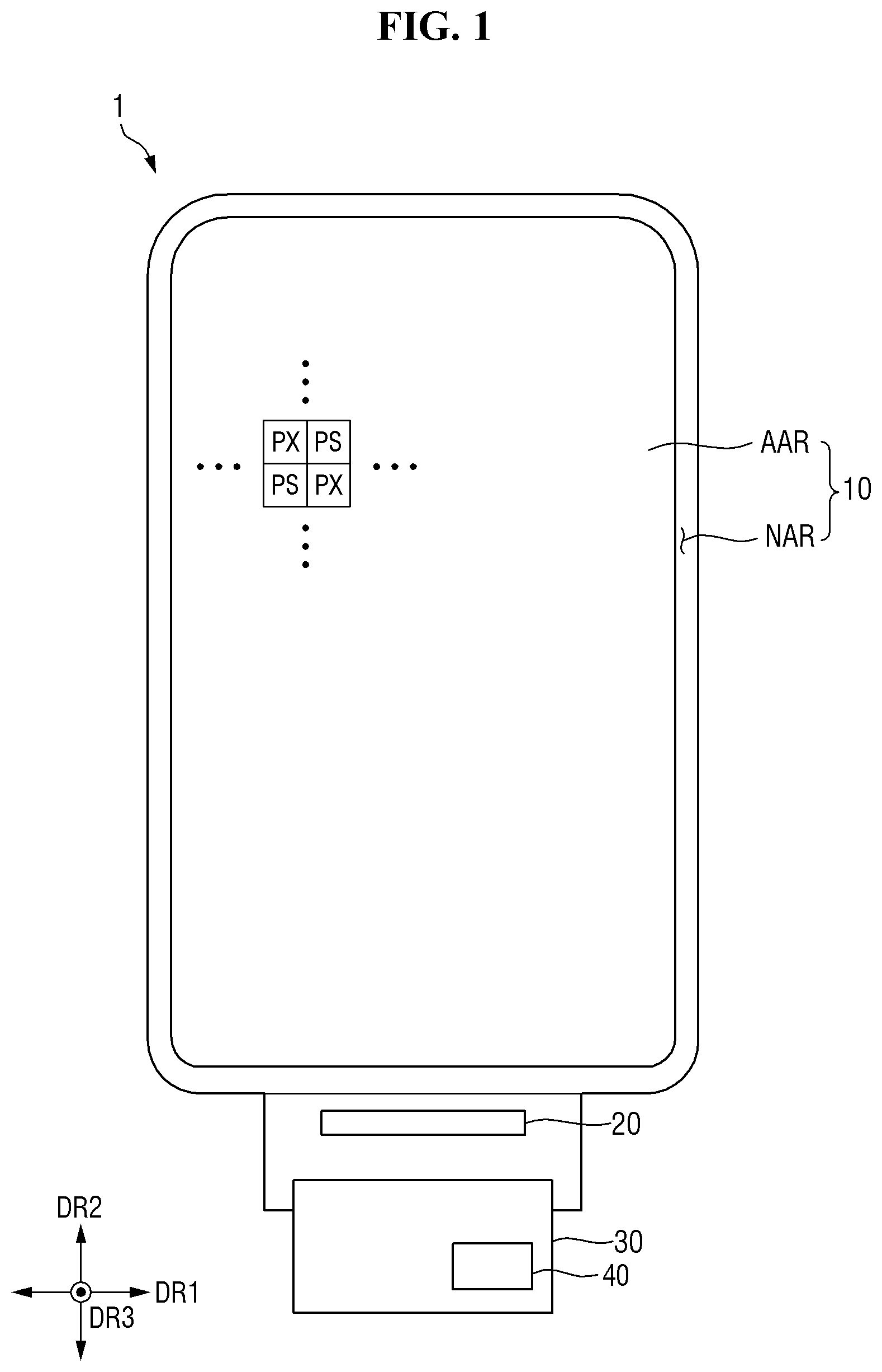
is a plan view illustrating a display device according to an embodiment of the present disclosure.
, a first direction DR 1 , a second direction DR 2 , and a third direction DR 3 are indicated. The first direction DR 1 may be a direction parallel to one side of a display device 1 in plan view and may be, for example, a horizontal direction of the display device 1 . The second direction DR 2 may be a direction parallel to the other side in contact with one side of the display device 1 in plan view and may be, for example, a vertical direction of the display device 1 .
Hereinafter, for simplicity of description, it is assumed that one side of the first direction DR 1 refers to a rightward direction in plan view, the other side of the first direction DR 1 refers to a leftward direction in plan view, one side of the second direction DR 2 refers an upward direction in plan view, and the other side of the second direction DR 2 refers to a downward direction in plan view, respectively. The third direction DR 3 may be a thickness direction of the display device 1 and may extend out of the page, in the plan view shown. It should be understood, however, that a direction mentioned in the embodiment refers to a relative direction and the embodiment is not necessarily limited to the direction mentioned.
Unless otherwise defined, with respect to the third direction DR 3 , the terms “above,” and “top surface” as used herein refer to a display surface's side of a display panel 10 , and the terms “below,” “bottom surface,” and “rear surface” as used herein refer to a side opposite to the display surface of the display panel 10 .
Referring to , the display device 1 may include various electronic devices that provide a display screen. Examples of the display device 1 may include, but are not necessarily limited to including, a mobile phone, a smart phone, a tablet personal computer (PC), a mobile communication terminal, an electronic notebook, an electronic book, a personal digital assistant (PDA), a portable multimedia player (PMP), a navigation device, an ultra-mobile PC (UMPC), a television, a game console, a wrist watch type electronic device, a head-mounted display, a personal computer monitor, a laptop computer, a car dashboard, a digital camera, a camcorder, an external billboard, an electric billboard, various medical devices, various inspection devices, various home appliances including a display area such as a refrigerator or a washing machine, an Internet-of-Things (IoT) device, and the like. A typical example of the display device 1 to be described later may be a smart phone, a tablet PC, or a laptop computer, but is not necessarily limited thereto.
The display device 1 may include a display panel 10 , a display driving circuit 20 , a circuit board 30 , and a read-out circuit 40 .
The display device 1 includes a display panel 10 having an active region AAR and a non-active region NAR. The active region AAR includes a display area on which an image is displayed. The active region AAR may completely overlap the display area. A plurality of pixels PX for displaying an image may be disposed within the display area. Each pixel PX may include a light emitting element (‘EL’ in ).
The active region AAR further includes a fingerprint sensing area. The fingerprint sensing area is a region that reacts to light, and is configured to sense the amount and/or wavelength of incident light. The fingerprint sensing area may overlap the display area. For example, the fingerprint sensing area may be disposed within a limited area necessary for fingerprint recognition within the active region AAR, rather than within an entirety of the display area. In this case, the fingerprint sensing area may overlap a portion of the display area while it does not overlap another portion of the display area. Alternatively, the fingerprint sensing area may be defined as an entire area of the active region AAR. In this case, the entire surface of the active region AAR may be utilized as an area for fingerprint sensing. A plurality of optical sensors PS that react to light may be disposed in the fingerprint sensing area. Each optical sensor PS may include a photoelectric conversion element‘PD’ in that detects incident light and converts the light into an electrical signal.
The non-active region NAR is disposed around the active region AAR. The non-active region NAR may be a bezel area of the display panel. The non-active region NAR may surround all sides (e.g., four sides in the drawing) of the active region AAR, but is not necessarily limited thereto, and may surround three, two, or even one side of the active region AAR.
The non-active region NAR may be disposed around the active region AAR. The display driving circuit 20 may be disposed in the non-active region NAR. The display driving circuit 20 may drive the plurality of pixels PX and/or the plurality of optical sensors PS. The display driving circuit 20 may output signals and voltages for driving the display panel 10 . The display driving circuit 20 may be formed as an integrated circuit (IC) and mounted on the display panel 10 . Signal lines for transferring signals between the display driving circuit 20 and the active region AAR may be further disposed in the non-active region NAR. For example, the display driving circuit 20 may be mounted on the circuit board 30 .
Signal lines for applying a signal to the active region AAR or the read-out circuit 40 may be disposed in the non-active region NAR. The read-out circuit 40 may be connected to each optical sensor PS through the signal line and may receive a current flowing in each optical sensor PS to detect a user's fingerprint input. The read-out circuit 40 may be formed as an integrated circuit (IC) and attached on a display circuit board in a chip on film (COF) structure, but is not necessarily limited thereto, and may be attached on the non-active region NAR of the display panel 10 in a chip on glass (COG) method, a chip on plastic (COP) method or an ultrasonic bonding method.
The circuit board 30 may be attached to one end of the display panel 10 using an anisotropic conductive film (ACF). Lead lines of the circuit board 30 may be electrically connected to a pad unit of the display panel 10 . The circuit board 30 may be a flexible film such as a flexible printed circuit board or a chip on film.
illustrates fingerprint sensing of a display device according to an embodiment of the present disclosure.
Referring to , the display device 1 may further include a window WDL disposed on the display panel 10 . The display panel 10 may include a substrate SUB, a display layer DPL disposed on the substrate SUB and including the pixels PX and the optical sensors PS, an encapsulation layer TFEL disposed on the display layer DPL, and a touch sensing layer TSL disposed on the encapsulation layer TFEL.
When the user's finger comes into contact with the top surface of the window WDL of the display device 1 , the light outputted from the pixels PX of the display panel 10 may be reflected from a ridge RID of a fingerprint F of the user and valleys VAL between the ridges RID. In this case, a portion of the ridge RID of the fingerprint F comes into contact with the top surface of the window WDL, whereas a portion of the valley VAL of the fingerprint F does not come into contact with the window WDL. For example, the top surface of the window WDL is in contact with the air at the valley VAL portion.
When the fingerprint F is in contact with the top surface of the window WDL, light outputted from emission portions of the pixels PX may be reflected from the ridge RID and the valley VAL of the fingerprint F. In this case, since the refractive index of the fingerprint F and the refractive index of the air are different, the amount of the light reflected from the ridge RID of the fingerprint F and the amount of the light reflected from the valley VAL of the fingerprint F may be different. Accordingly, the ridge RID portion and the valley VAL portion of the fingerprint F may be detected based on a difference in the amount of the reflected light, for example, the light incident on the optical sensors PS. Since the optical sensor PS outputs an electrical signal (i.e., photocurrent) according to the difference in the amount of light, the pattern of the fingerprint F of the finger may be identified.
is a schematic plan layout view of a display layer according to an embodiment of the present disclosure.
Referring to , in the active region AAR of the display layer DPL, scan lines SL and power voltage lines VL connected to the plurality of pixels PX and the plurality of optical sensors PS, emission control lines EML and data lines DL connected to the plurality of pixels PX, and a reset control line RSTL and a read-out line ROL connected to the plurality of optical sensors PS may be disposed.
The scan line SL may supply the scan signal received from a scan driver SDC to the plurality of pixels PX and the plurality of optical sensors PS. The scan lines SL may extend in the first direction DR 1 and may be spaced apart from each other in the second direction DR 2 .
The emission control line EML may supply the emission control signal received from the scan driver SDC to the plurality of pixels PX. The emission control lines EML may extend in the first direction DR 1 and may be spaced apart from each other in the second direction DR 2 .
The data line DL may supply the data voltage received from the display driving circuit 20 to the plurality of pixels PX. The data lines DL may extend in the second direction DR 2 and may be spaced apart from each other in the first direction DR 1 .
The power voltage line VL may supply the power voltage received from the display driving circuit 20 to the plurality of pixels PX and the plurality of optical sensors PS. Here, the power voltage may be at least one of a driving power voltage ELVDD, a common voltage ELVSS, a first initialization voltage VINT, and a second initialization voltage VAINT. The driving power voltage ELVDD may be a relatively high potential voltage for driving the light emitting element and the photoelectric conversion element, and the common voltage ELVSS may be a relatively low potential voltage for driving the light emitting element and the photoelectric conversion element. For example, the driving power voltage ELVDD may have a higher potential than the common voltage ELVSS. The power voltage lines VL may extend from the active region AAR in the second direction DR 2 , may be spaced apart from each other in the first direction DR 1 , and may be connected to each other in the non-active region NAR.
The reset control line RSTL may supply the reset control signal received from the scan driver SDC to the plurality of optical sensors PS. The reset control lines RSTL may extend in the first direction DR 1 and may be spaced apart from each other in the second direction DR 2 .
The read-out line ROL may supply a sensing current generated in the optical sensor PS according to external light to the read-out circuit 40 of . The read-out lines ROL may extend in the second direction DR 2 and may be spaced apart from each other in the first direction DR 1 .
The non-active region NAR of the display layer DPL may include the scan driver SDC and a display driving circuit 20 .
The scan driver SDC may generate a plurality of scan signals based on the scan control signal, and may sequentially supply the plurality of scan signals to the plurality of scan lines SL according to a set order. In addition, the scan driver SDC may sequentially supply the emission control signal to the plurality of emission control lines EML according to a set order. The scan driver SDC may sequentially supply the reset control signal to the plurality of reset control lines RSTL according to a set order.
The display driving circuit 20 may output signals and voltages for driving the display panel 10 . The display driving circuit 20 may supply a data voltage to the data line DL. The data voltage may be supplied to the plurality of pixels PX, and the luminance of the plurality of pixels PX may be determined.
The non-active region NAR may include a read-out circuit. The read-out circuit may be connected to each optical sensor PS through the read-out line ROL, and may generate fingerprint detection data according to the magnitude of current sensed by each optical sensor PS to transmit the fingerprint detection data to the main processor. By analyzing the fingerprint sensing data, the main processor may determine whether the fingerprint detection data matches the user's fingerprint by comparing the fingerprint detection data with a preset fingerprint. When the preset fingerprint and the fingerprint sensing data transmitted from the read-out circuit are the same, the set functions may be performed.
The non-active region NAR of the display layer DPL may further include a display pad unit DPD and first and second touch pad units TPD 1 and TPD 2 . The display pad unit DPD, the first touch pad unit TPD 1 , and the second touch pad unit TPD 2 may be electrically connected to the circuit board 30 by using a low-resistance high-reliability material such as an anisotropic conductive film or SAP. The display pad unit DPD may include a plurality of display pads.
In the present embodiment, each scan line SL is illustrated as being simultaneously connected to the plurality of pixels PX and the plurality of optical sensors PS, but the present disclosure is not necessarily limited thereto, and the type and disposition shape of the signal lines may vary. In this case, the plurality of pixels PX and the plurality of optical sensors PS may be turned on or off based on the same scan signal. Accordingly, the shape of the fingerprint may be optically sensed during the period when the screen is displayed.
is a circuit diagram illustrating a pixel and an optical sensor according to an embodiment of the present disclosure.
, for simplicity of description, exemplifies a circuit diagram of the pixel PX connected to a k scan initialization line G 1 Lk, a k th scan write line GWLk, a k th scan control line GCLk, a (k−1) th scan write line GWLk-1, and a j th data line DLj, and the optical sensor PS connected to the k th scan write line GWLk, a k th reset control line RSTLk, and a q th read-out line ROLq.
The pixel PX may include a light emitting element EL and a pixel driving unit controlling the emission amount of the light emitting element EL. The pixel driving unit may include a driving transistor DT, a plurality of switch elements, and a first capacitor Cst. The switch elements include first to sixth transistors T 1 , T 2 , T 3 , T 4 , T 5 , and T 6 . The pixel driving unit may be connected to a driving voltage line VDL to which the driving voltage ELVDD is applied, a common voltage line VSL to which the common voltage ELVSS is applied, a first initialization voltage line VIL 1 to which the first initialization voltage VINT is applied, and a second initialization voltage line VIL 2 to which the second initialization voltage VAINT is applied.
The driving transistor DT may include a gate electrode, a first electrode, and a second electrode. The driving transistor DT controls a drain-source current Isd (hereinafter, referred to as “driving current”) flowing between the first electrode and the second electrode according to a data voltage applied to the gate electrode. The driving current Isd flowing through a channel of the driving transistor DT is proportional to the square of the difference between a threshold voltage and a voltage Vgs between the first electrode and the gate electrode of the driving transistor DT, as shown in Equation 1. Isd=k ′×( Vsg−Vth ) 2 [Equation 1]
In Equation 1, Isd is a source-drain current flowing through the channel of the driving transistor DT as a driving current, k th is a proportional coefficient determined by the structure and physical characteristics of the driving transistor, Vsg is a voltage between the first electrode and the gate electrode of the driving transistor, and Vth is the threshold voltage of the driving transistor.
The light emitting element EL emits light by the driving current Isd. As the driving current Isd increases, the amount of light emitted from the light emitting element EL may increase.
The light emitting element EL may be an organic light emitting diode including an organic light emitting layer disposed between an anode electrode and a cathode electrode. Alternatively, the light emitting element EL may be a quantum dot light emitting element including a quantum dot light emitting layer disposed between an anode electrode and a cathode electrode.
Alternatively, the light emitting element EL may be an inorganic light emitting element including an inorganic semiconductor disposed between an anode electrode and a cathode electrode. When the light emitting element EL is an inorganic light emitting element, a micro light emitting diode or a nano light emitting diode may be included. In , the anode electrode of the light emitting element EL corresponds to a pixel electrode 170 , and the cathode electrode thereof corresponds to a common electrode 190 .
The anode electrode of the light emitting element EL may be connected to the second electrode of the fifth transistor T 5 and the first electrode of the sixth transistor T 6 , and the cathode electrode may be connected to the common voltage line VSL to which the common voltage ELVSS is applied.
The first transistor T 1 is turned on by the k th scan write signal of the k th scan write line GWLk to connect the first electrode of the driving transistor DT to the j th data line DLj. Accordingly, the data voltage of the j th data line DLj may be applied to the first electrode of the driving transistor DT. The gate electrode of the first transistor T 1 may be connected to the k th scan write line GWLk, the first electrode thereof may be connected to the j th data line DLj, and the second electrode thereof may be connected to the first electrode of the driving transistor DT.
The second transistor T 2 is turned on by the k th scan control signal of the k th scan control line GCLk to connect the gate electrode of the driving transistor DT to the second electrode of the driving transistor DT. When the gate electrode of the driving transistor DT is connected to the second electrode thereof, the driving transistor DT is driven as a diode. The gate electrode of the second transistor T 2 may be connected to the k th scan control line GCLk, the first electrode may be connected to the gate electrode of the driving transistor DT, and the second electrode may be connected to the second electrode of the driving transistor DT.
The third transistor T 3 is turned on by the k th scan initialization signal of the k th scan initialization line GILk to connect the gate electrode of the driving transistor DT to the first initialization voltage line VIL 1 . Accordingly, the first initialization voltage VINT 1 of the first initialization voltage line VIL 1 may be applied to the gate electrode of the driving transistor DT. The gate electrode of the third transistor T 3 may be connected to the k th scan initialization line GILk, the first electrode thereof may be connected to the first initialization voltage line VIL 1 , and the second electrode thereof may be connected to the gate electrode of the driving transistor DT.
The fourth transistor T 4 is turned on by the k th emission control signal of the k th emission control line EMLk to connect the first electrode of the driving transistor DT to the driving voltage line VDL to which the driving voltage ELVDD is applied. The gate electrode of the fourth transistor T 4 may be connected to the k th emission control line EMLk, the first electrode thereof may be connected to the driving voltage line VDL, and the second electrode thereof may be connected to the first electrode of the driving transistor DT.
The fifth transistor T 5 is turned on by the k th emission control signal of the k th emission control line EMLk to connect the second electrode of the driving transistor DT to the anode electrode of the light emitting element EL. The gate electrode of the fifth transistor T 5 may be connected to the k th emission control line EMLk, the first electrode thereof may be connected to the second electrode of the driving transistor DT, and the second electrode thereof may be connected to the anode electrode of the light emitting element EL.
When both the fourth transistor T 4 and the fifth transistor T 5 are turned on, the driving current Isd of the driving transistor DT according to the voltage of the gate electrode of the driving transistor DT may flow through the light emitting element EL.
The sixth transistor T 6 is turned on by the (k−1) th scan signal of the (k−1) th scan write line GWLk−1 to connect the anode electrode of the light emitting element EL to the second initialization voltage line VIL 2 . The second initialization voltage VAINT of the second initialization voltage line VIL 2 may be applied to the anode electrode of the light emitting element EL. The gate electrode of the sixth transistor T 6 may be connected to the (k−1) th scan write line GWLk−1, the first electrode thereof may be connected to the anode electrode of the light emitting element EL, and the second electrode thereof may be connected to the second initialization voltage line VIL 2 .
The first capacitor Cst is formed between the gate electrode of the driving transistor DT and the driving voltage line VDL. The first capacitor electrode of the first capacitor Cst may be connected to the gate electrode of the driving transistor DT, and the second capacitor electrode thereof may be connected to the driving voltage line VDL.
When the first electrode of each of the driving transistor DT and the first to sixth transistors T 1 , T 2 , T 3 , T 4 , T 5 , and T 6 is a source electrode, the second electrode thereof may be a drain electrode. Alternatively, when the first electrode of each of the driving transistor DT and the first to sixth transistors T 1 , T 2 , T 3 , T 4 , T 5 , and T 6 is a drain electrode, the second electrode thereof may be a source electrode.
The active layer of each of the driving transistor DT and the first to sixth transistors T 1 , T 2 , T 3 , T 4 , T 5 , and T 6 may also be formed of any one of polysilicon, amorphous silicon, and oxide semiconductor. For example, the active layer of each of the driving transistor DT, the first transistor T 1 , and the fourth to sixth transistors T 4 to T 6 may be made of polysilicon. The active layer of each of the second transistor T 2 and the third transistor T 3 may be formed of an oxide semiconductor. In this case, the driving transistor DT, the first transistor T 1 , and the fourth to sixth transistors T 4 to T 6 may be formed of a P-type MOSFET, and the second transistor T 2 and the third transistor T 3 may also be formed of an N-type MOSFET.
Each of the plurality of optical sensors PS may include a photoelectric conversion element PD and a sensing driver controlling a sensing current according to a photocurrent of the photoelectric conversion element PD. The sensing driver includes a plurality of sensing transistors LT 1 , LT 2 , and LT 3 for controlling a sensing current generated by the photoelectric conversion element PD. The sensing driver may be connected to a reset voltage line VRL to which a reset voltage Vrst is applied, the second initialization voltage line VIL 2 to which the second initialization voltage VAINT is applied, and the common voltage line VSL to which the common voltage ELVSS is applied.
Each of the photoelectric conversion elements PD may be a photodiode including a sensing anode electrode, a sensing cathode electrode, and a photoelectric conversion layer disposed between the sensing anode electrode and the sensing cathode electrode. Each of the photoelectric conversion elements PD may convert externally incident light into an electrical signal. The photoelectric conversion element PD may be an inorganic photodiode or a phototransistor formed of a pn-type or pin-type inorganic material. Alternatively, the photoelectric conversion element PD may also be an organic photodiode including an electron donating material generating donor ions and an electron accepting material generating acceptor ions. In , the sensing anode electrode of the photoelectric conversion element PD corresponds to a first electrode 180 , and the sensing cathode electrode corresponds to the common electrode 190 .
When the photoelectric conversion element PD is exposed to external light, photocharges may be generated, and the generated photocharges may be accumulated in the sensing anode electrode of the photoelectric conversion element PD. In this case, the voltage of a first node N 1 electrically connected to the sensing anode electrode may increase. When the photoelectric conversion element PD and the q th read-out line ROLq are connected according to the turn-on of the first and third sensing transistors LT 1 and LT 3 , a sensing voltage may be accumulated at the third node N 3 between the qh read-out line ROLq and the third sensing transistor LT 3 in proportion to the voltage of the first node N 1 in which the electric charges are accumulated.
The first sensing transistor LT 1 may be turned on by the voltage of the first node N 1 applied to the gate electrode to connect the second initialization voltage line VIL 2 to the second electrode of the third sensing transistor LT 3 . The gate electrode of the first sensing transistor LT 1 may be connected to the first node N 1 , the first electrode thereof may be connected to the second initialization voltage line VIL 2 , and the second electrode thereof may be connected to the first electrode of the third sensing transistor LT 3 . The first sensing transistor LT 1 may be a source follower amplifier that generates a source-drain current in proportion to the amount of electric charges of the first node N 1 inputted to the gate electrode thereof. Although the first electrode of the first sensing transistor LT 1 is illustrated as being connected to the second initialization voltage line VIL 2 , the present disclosure is not necessarily limited thereto, and the first electrode of the first sensing transistor LT 1 may also be connected to the driving voltage line VDL or the first initialization voltage line VILL.
The second sensing transistor LT 2 may be turned on by the k th reset control signal of the k th reset control line RSTLk to connect the first node N 1 to the reset voltage line VRL applying the reset voltage Vrst. The gate electrode of the second sensing transistor LT 2 may be connected to the k th reset control line RSTLk, the first electrode thereof may be connected to the reset voltage line VRL, and the second electrode thereof may be connected to the first node N.
The third sensing transistor LT 3 may be turned on by the k th scan write signal of the k th scan write line GWLk to connect the second electrode of the first sensing transistor LT 1 and the q th read-out line ROLq. The gate electrode of the third sensing transistor LT 3 may be connected to the k th scan write line GWLk, the first electrode thereof may be connected to the second electrode of the first sensing transistor LT 1 , and the second electrode thereof may be connected to the third node N 3 and the q th read-out line ROLq.
An active layer of each of the first to third sensing transistors LT 1 , LT 2 , and LT 3 may also be formed of any one of polysilicon, amorphous silicon, and an oxide semiconductor. For example, the active layer of the first sensing transistor LT 1 and the third sensing transistor LT 3 may be made of polysilicon. The active layer of the second sensing transistor LT 2 may be formed of an oxide semiconductor. In this case, the first sensing transistor LT and the third sensing transistor LT 3 may be formed of a P-type MOSFET, and the second sensing transistor LT 2 may also be formed of an N-type MOSFET.
is a schematic plan layout view of a touch sensing layer of a display panel according to an embodiment of the present disclosure.
Referring to , the touch sensing layer TSL includes the active region AAR and the non-active region NAR. The active region AAR may be a touch sensing area for sensing a user's touch, and the non-active region NAR may be a touch peripheral area disposed in the periphery of the touch sensing area. The touch sensing area may overlap the display area and the fingerprint sensing area of the display layer DPL described above, and may overlap the non-display area of the display layer DPL described above in the touch peripheral area.
The active region AAR may include a plurality of first touch electrodes IE 1 and a plurality of second touch electrodes IE 2 . One of the first touch electrode IE 1 and the second touch electrode IE 2 may be a driving electrode, and the other may be a sensing electrode. In the present embodiment, the case where the first touch electrode IE 1 is a driving electrode and the second touch electrode IE 2 is a sensing electrode is exemplified.
The first touch electrode IE 1 may extend in the second direction DR 2 . The first touch electrode IE 1 may include a plurality of first sensor portions SP 1 arranged along the second direction DR 2 and a first connection portion CP 1 electrically connecting the adjacent first sensor portions SP 1 to each other. The plurality of first touch electrodes IE 1 may be arranged in the first direction DR 1 .
The second touch electrode IE 2 may extend in the first direction DR 1 . The second sensing electrode IE 2 may include a plurality of second sensor portions SP 2 arranged in the first direction DR 1 and a second connection portion CP 2 electrically connecting the adjacent second sensor portions SP 2 to each other. The plurality of second touch electrodes IE 2 may be arranged in the second direction DR 2 .
At least some of the first sensor portions SP 1 and the second sensor portions SP 2 may have a rhombic shape. Some of the first sensor portions SP 1 and the second sensor portions SP 2 may have a shape of a figure cut from a rhombus (e.g., a rhombic section). For example, each of the first sensor portions SP 1 and the second sensor portions SP 2 positioned at both ends in the extension direction may have a triangular shape obtained by cutting a rhombus in half. The first sensor portions SP 1 having a rhombic or triangular shape and the second sensor portions SP 2 having a rhombic or triangular shape may have substantially the same size and shape. However, the embodiment is not necessarily limited to the above example, and the shapes and sizes of the first sensor portion SP 1 and the second sensor portion SP 2 may be variously modified.
The first connection portion CP may connect the corner portions of the adjacent rhombic or triangular first sensor portions SP 1 to each other. The second connection portion CP 2 may connect the corner portions of the adjacent rhombic or triangular second sensor portions SP 2 to each other. The widths of the first connection portion CP 1 and the second connection portion CP 2 may be smaller than the widths of the first sensor portion SP 1 and the second sensor portion SP 2 .
The first touch electrode IE 1 and the second touch electrode IE 2 may be electrically insulated from each other and may intersect each other. Insulation between the first touch electrode IE 1 and the second touch electrode IE 2 may be ensured by being connected through conductive layers positioned on different layers in the intersecting region. Intersection between the first touch electrode IE 1 and the second touch electrode IE 2 may be achieved by the first connection portion CP 1 and/or the second connection portion CP 2 . For the insulation and intersection, at least one of the first connection portion CP 1 or the second connection portion CP 2 may be positioned on a different layer from the first touch electrode IE 1 and the second touch electrode IE 2 . The stacked structure of the touch sensing layer TSL will be described with reference to .
The first sensor portions SP 1 and the second sensor portions SP 2 adjacent to each other may constitute a unit sensing area SUT. For example, half of two adjacent first sensor portions SP 1 and half of two adjacent second sensor portions SP 2 with respect to a region where the first touch electrode IE 1 and the second touch electrode IE 2 intersect may constitute a single square or rectangle. As described above, an area defined by the half areas of the two adjacent first and second sensor portions SP 1 and SP 2 may be one unit sensing area SUT. A plurality of unit sensing areas SUT may be arranged in a matrix.
In each unit sensing area SUT, by measuring the capacitance value between the adjacent first and second sensor portions SP 1 and SP 2 , it is possible to determine whether or not a touch is inputted and to calculate the corresponding position as touch input coordinates. The touch sensing may be performed in a mutual cap method, but is not necessarily limited thereto.
Each unit sensing area SUT may be larger in size than a pixel. For example, the unit sensing area SUT may correspond to the size of a plurality of pixels. For example, length of one side of the unit sensing area SUT may be in the range of 4 to 5 mm, but is not necessarily limited thereto.
A plurality of touch signal lines are disposed in the non-active region NAR. The touch signal line extends from the first and second touch pad units TPD 1 and TPD 2 to the non-active region NAR.
The plurality of touch signal lines includes a plurality of touch driving lines TL (TL 1 and TL 2 ) and a plurality of touch sensing lines RL. The plurality of touch signal lines may further include a touch ground line and/or a touch antistatic line.
The touch driving line TL may be connected to the first touch electrode 1 El. In an embodiment of the present disclosure, a plurality of touch driving lines may be connected to the one first touch electrode IE 1 . For example, the touch driving line TL may include a first touch driving line TL 1 connected to a lower end of the first touch electrode IE 1 and a second touch driving line TL 2 connected to an upper end of the first touch electrode IE 1 . The first touch driving line TL 1 may extend from the first touch pad unit TPD 1 to one side in the second direction DR 2 and may be connected to the lower end of the first touch electrode IE 1 . The second touch driving line TL 2 may extend from the first touch pad unit TPD 1 to one side in the second direction DR 2 and bypass the left edge of the active region AAR (or the touch sensing area) and may be connected to the upper end of the first touch electrode IE 1 .
The touch sensing line RL may be connected to the second touch electrode IE 2 . In an embodiment of the present disclosure, one touch sensing line RL may be connected to one second touch electrode IE 2 . Each touch sensing line RL may extend from the second touch pad unit TPD 2 to one side in the second direction DR 2 and extend toward the right edge of the active region AAR (or touch sensing area) and may connected to a right end of the second touch electrode IE 2 .
When the first touch electrode IE 1 and the second touch electrode IE 2 are driven by a mutual capacitance method, a driving signal is applied to the first touch electrode IE 1 through the first and second touch driving lines TL 1 and TL 2 , and the capacitance formed in the unit sensing area SUT is charged. Thereafter, a change in capacitance of the second touch electrode IE 2 is measured through the touch sensing line RL to determine whether a touch is inputted.
is an enlarged view illustrating a pixel and an optical sensor of a display layer and touch electrodes of a touch sensing layer according to an embodiment of the present disclosure.
The display layer DPL includes the plurality of pixels PX and the plurality of optical sensors PS. The plurality of pixels PX may include a plurality of light emitting units EMA (EMA 1 , EMA 2 , EMA 3 , and EMA 4 ) that each emit light in the active region AAR (or the display area). The plurality of light emitting units EMA may be defined as areas in which the pixel electrode 170 is exposed by the opening of the pixel defining layer 160 in the cross-sectional view of , and may be defined as areas in which the exposed pixel electrode 170 and the light emitting layer 175 overlap. The first light emitting unit EMA 1 may emit first light of a red wavelength band (e.g., red light). The second light emitting unit EMA 2 and the fourth light emitting unit EMA 4 may emit second light of a green wavelength band (e.g., green light). The third light emitting unit EMA 3 may emit third light of a blue wavelength band (e.g., blue light).
The plurality of optical sensors PS may include a plurality of light sensing units RA that sense light incident within the active region AAR (or fingerprint sensing area). The light sensing unit RA may be defined as an area in which the first electrode 180 is exposed by the opening of the pixel defining layer 160 in cross-sectional view, and may be defined as an area in which the exposed first electrode 180 and the photoelectric conversion layer 185 overlap.
A non-emission area is disposed between the light emitting units EMA of each pixel PX. In addition, a non-sensing area is disposed between the light sensing units RA of each optical sensor PS. In the present specification, an area in which the non-emission area and the non-sensing area overlap will be referred to as a peripheral portion NEA. The pixel defining layer 160 may be disposed in the peripheral portion NEA.
The plurality of light emitting units EMA 1 , EMA 2 , EMA 3 , and EMA 4 may be spaced apart from each other in the first direction DR 1 and the second direction DR 2 . For example, the first light emitting unit EMA 1 and the third light emitting unit EMA 3 may be alternately arranged in the first direction DR 1 and the second direction DR 2 . The second light emitting unit EMA 2 and the fourth light emitting unit EMA 4 may be alternately arranged in the first direction DR 1 and the second direction DR 2 .
The plurality of light emitting units EMA 1 , EMA 2 , EMA 3 , and EMA 4 may be alternately disposed in diagonal directions DD 1 and DD 2 between the first direction DR 1 and the second direction DR 2 . The first diagonal direction DD 1 may be a direction inclined at 45° with respect to the first direction DR 1 and the second direction DR 2 , and the second diagonal direction DD 2 may be a direction intersecting the first diagonal direction DDL. For example, the first light emitting unit EMA 1 and the fourth light emitting unit EMA 4 may be alternately arranged in the first diagonal direction DD 1 . The third light emitting unit EMA 3 and the second light emitting unit EMA 2 may be alternately arranged in the first diagonal direction DD 1 . The first light emitting unit EMA 1 and the second light emitting unit EMA 2 may be alternately arranged in the second diagonal direction DD 2 , and the third light emitting unit EMA 3 and the fourth light emitting unit EMA 4 may be alternately arranged in the second diagonal direction DD 2 .
The light sensing unit RA may be disposed between the second light emitting unit EMA 2 and the fourth light emitting unit EMA 4 adjacent in the first direction DR 1 , and may be disposed between the first light emitting unit EMA 1 and the third light emitting unit EMA 3 adjacent in the second direction DR 2 .
The plurality of light emitting units EMA 1 , EMA 2 , EMA 3 , and EMA 4 may have different sizes. The size of the first light emitting unit EMA 1 may be greater than the size of the second light emitting unit EMA 2 and the fourth light emitting unit EMA 4 , and may be smaller than the size of the third light emitting unit EMA 3 . The size of the second light emitting unit EMA 2 may be substantially the same as the size of the fourth light emitting unit EMA 4 .
The first light emitting unit EMA 1 , the second light emitting unit EMA 2 , the third light emitting unit EMA 3 , and the fourth light emitting unit EMA 4 may have an octagonal planar shape, but are not necessarily limited thereto. The first light emitting unit EMA 1 , the second light emitting unit EMA 2 , the third light emitting unit EMA 3 , and the fourth light emitting unit EMA 4 may have a quadrilateral planar shape such as a rhombus or another polygonal planar shape. In addition, each of the light sensing units RA may have a quadrilateral planar shape, but is not necessarily limited thereto. Each of the light sensing units RA may have a planar shape of a rhombus, an octagon, or another polygon.
The first touch electrode IE 1 and the second touch electrode IE 2 of the touch sensing layer TSL may include an electrode pattern MP of a mesh shape. The electrode pattern MP may be disposed along a boundary between the pixel PX and the optical sensor PS in the peripheral portion NEA. The electrode pattern MP might not overlap the light emitting unit EMA and the light sensing unit RA. A width of the electrode pattern MP in one direction may be smaller than a width of the peripheral portion NEA in one direction (e.g., in the same one direction).
The electrode pattern MP may include a plurality of first electrode lines 410 extending in the first direction DR 1 , a plurality of second electrode lines 420 extending in the second direction DR 2 , a plurality of third electrode lines 430 extending in the first diagonal direction DD 1 , and a plurality of fourth electrode lines 440 extending in the second diagonal direction DD 2 .
Each of the first electrode lines 410 may be disposed outside the light sensing unit RA, the first light emitting unit EMA 1 , or the third light emitting unit EMA 3 . Each of the second electrode lines 420 may be disposed outside the light sensing unit RA, the second light emitting unit EMA 2 , or the fourth light emitting unit EMA 4 . Each of the third electrode lines 430 may be disposed outside any one of the first to fourth light emitting units EMA 1 , EMA 2 , EMA 3 , and EMA 4 . Each of the fourth electrode lines 440 may be disposed outside any one of the first to fourth light emitting units EMA 1 , EMA 2 , EMA 3 , and EMA 4 .
In the present embodiment, the light sensing unit RA may be disposed in a mesh hole formed by the first electrode lines 410 and the second electrode lines 420 that intersect. The two first electrode lines 410 and the two second electrode lines 420 surrounding the light sensing unit RA may have a quadrilateral planar shape, but are not necessarily limited thereto. For example, the mesh hole in which the light sensing unit RA is disposed may have a quadrilateral planar shape.
The first light emitting unit EMA 1 or the third light emitting unit EMA 3 may be disposed in the mesh hole formed by the first electrode lines 410 , the third electrode lines 430 , and the fourth electrode lines 440 that intersect. The two first electrode lines 410 , the two third electrode lines 430 , and the two fourth electrode lines 440 surrounding the first light emitting unit EMA 1 or the third light emitting unit EMA 3 may have a hexagonal planar shape. For example, the mesh hole in which the first light emitting unit EMA 1 or the third light emitting unit EMA 3 is disposed may have a hexagonal planar shape having two sides parallel to the second direction DR 2 .
The second light emitting unit EMA 2 or the fourth light emitting unit EMA 4 may be disposed in the mesh hole formed by the second electrode lines 420 , the third electrode lines 430 , and the fourth electrode lines 440 that intersect. The two second electrode lines 420 , the two third electrode lines 430 , and the two fourth electrode lines 440 surrounding the second light emitting unit EMA 2 or the fourth light emitting unit EMA 4 may have a hexagonal planar shape. For example, the mesh hole in which the second light emitting unit EMA 2 or the fourth light emitting unit EMA 4 is disposed may have a hexagonal planar shape having two sides parallel to the first direction DR 1 .
For example, since the planar shape of the mesh hole in which the plurality of light sensing units RA are disposed is a quadrilateral shape, and the planar shape of the mesh hole in which the plurality of light emitting units EMA 1 , EMA 2 , EMA 3 , and EMA 4 are disposed is an octagonal shape, the planar shapes may be different from each other. In addition, a planar shape of the plurality of light sensing units RA may be different from a planar shape of a mesh hole in which the plurality of light sensing units RA are disposed. For an example, the planar shape of the plurality of light sensing units RA may be the same quadrilateral shape as the planar shape of a mesh hole in which the plurality of light sensing units RA are disposed. A planar shape of the plurality of light emitting units EMA 1 , EMA 2 , EMA 3 , and EMA 4 may be an octagonal shape, and a shape of a mesh hole in which the plurality of light emitting units EMA 1 , EMA 2 , EMA 3 , and EMA 4 are disposed may be a hexagonal shape, so that the shapes are different from each other.
Each of the mesh holes may be defined by an electrode pattern MP of the first touch electrodes IE 1 and the second touch electrodes IE 2 . Each of the mesh holes may be included in the peripheral portion NEA. Although it is illustrated that the mesh holes correspond one-to-one to the plurality of light emitting units EMA 1 , EMA 2 , EMA 3 , and EMA 4 in the present embodiment, the present disclosure is not necessarily limited thereto. Each of the mesh holes may also correspond to the two or more light emitting units EMA 1 , EMA 2 , EMA 3 , and EMA 4 .
In addition, the sizes of the mesh holes in which the plurality of light emitting units EMA 1 , EMA 2 , EMA 3 , and EMA 4 and the plurality of light sensing units RA are disposed may also be different from each other or may also be the same.
All of the first to fourth electrode lines 410 , 420 , 430 , and 440 corresponding to one first sensor portion SP 1 may be physically connected. The first to fourth electrode lines 410 , 420 , 430 , and 440 corresponding to one second sensor portion SP 2 may all be physically connected. The first to fourth electrode lines 410 , 420 , 430 , and 440 included in one first sensor portion SP 1 may be spaced apart from the first to fourth electrode lines 410 , 420 , 430 , and 440 included in the other first sensor portion SP 1 . In addition, the first to fourth electrode lines 410 , 420 , 430 , and 440 included in one first sensor portion SP 1 may be spaced apart from the first to fourth electrode lines 410 , 420 , 430 , and 440 included in one second sensor portion SP 2 .
The adjacent first sensor portions SP 1 may be electrically connected to each other by the first connection portions CP 1 (CP 1 _ 1 and CP 1 _ 2 ) disposed on a different conductive layer. The first sensor portion SP 1 and the first connection portion CP 1 may be connected in first contact areas CA 1 including first contact holes CNT 1 . Although one first connection portion CP 1 is disconnected, the first sensor portions SP 1 adjacent to each other by the other first connection portion CP 1 may maintain electrical connection. The adjacent second sensor portions SP 2 may be electrically connected to each other by the second connection portion CP 2 disposed on the same conductive layer.
The display device 1 _ 1 , according to the present embodiment, may include the plurality of light emitting units EMA 1 , EMA 2 , EMA 3 , and EMA 4 and the plurality of light sensing units RA. The plurality of first touch electrodes IE 1 and the plurality of second touch electrodes IE 2 disposed on the plurality of light emitting units EMA 1 , EMA 2 , EMA 3 , and EMA 4 and the plurality of light sensing units RA may have the electrode pattern MP of a mesh shape. Accordingly, the plurality of first touch electrodes IE 1 and the plurality of second touch electrodes IE 2 do not overlap the plurality of light emitting units EMA 1 , EMA 2 , EMA 3 , EMA 4 and the plurality of light sensing units RA, and thus the light emitted from the light emitting units EMA 1 , EMA 2 , EMA 3 , and EMA 4 may be prevented from being blocked by the plurality of first touch electrodes IE 1 and the plurality of second touch electrodes IE 2 , or the light incident on the light sensing unit RA may be prevented from being blocked. For example, the plurality of first touch electrodes IE 1 and the plurality of second touch electrodes IE 2 might not be visually recognized by a user, and external light may be stably incident on the light sensing unit RA.
is an enlarged view illustrating area A of in detail.
illustrates a portion of one first connection portion CP 1 _ 1 , one first sensor portion SP 1 , and one second sensor portion SP 2 , but the same may be applied to the other first connection portion CP 1 _ 2 .
The electrode pattern MP may include the first contact area CA 1 connecting the first to fourth electrode lines 410 , 420 , 430 , and 440 spaced apart from each other. The first contact area CA 1 may be an area that connects the first sensor portion SP 1 to the first connection portion CP 1 _ 1 through the first contact hole CNT 1 .
In the present embodiment, each of the first contact areas CA 1 might not be disposed between the light sensing unit RA and the plurality of light emitting units EMA 1 , EMA 2 , EMA 3 , and EMA 4 adjacent to each other. For example, the first contact area CA 1 might not be disposed on the first electrode lines 410 or the second electrode lines 420 surrounding the light sensing unit RA.
For example, each of the first contact areas CA 1 may be disposed between the first light emitting unit EMA 1 and the third light emitting unit EMA 3 alternately arranged in the first direction DR 1 . Each of the first contact areas CA 1 may be disposed between the second light emitting unit EMA 2 and the fourth light emitting unit EMA 4 alternately arranged in the second direction DR 2 . For example, the first contact area CA 1 may be formed in a region where the third electrode line 430 and the fourth electrode line 440 intersect each other. The third electrode line 430 and the fourth electrode line 440 are disposed to surround the first light emitting unit EMA 1 , the second light emitting unit EMA 2 , the third light emitting unit EMA 3 , and the fourth light emitting unit EMA 4 that are adjacent.
Accordingly, a second width W 2 of the first contact area CA 1 in one direction may be greater than a first width W 1 of the electrode pattern MP in one direction not disposed in the first contact area CA 1 . For example, the second width W 2 of the first contact area CA 1 may be greater than the first width W 1 of each of the first to fourth electrode lines 410 , 420 , 430 , and 440 . One direction may be the first direction DR 1 , the second direction DR 2 , the first diagonal direction DD 1 , or the second diagonal direction DD 2 . For example, the second width W 2 may have about 12 μm, and the first width W 1 may have about 4 μm. For example, the first contact area CA 1 may have a sufficient width to form the first contact hole CNT 1 .
In the present embodiment, the plurality of light sensing units RA may be disposed between the plurality of light emitting units EMA 1 , EMA 2 , EMA 3 , and EMA 4 , and thus the minimum distance between the light sensing unit RA and the light emitting units EMA 1 , EMA 2 , EMA 3 , and EMA 4 that are adjacent may be smaller than the minimum distance among the light emitting units EMA 1 , EMA 2 , EMA 3 , and EMA 4 . Accordingly, since the first contact area CA 1 may be disposed on the electrode pattern MP having a sufficient width to form the first contact hole CNT 1 , the first contact area CA 1 might not be disposed on the first electrode lines 410 and the second electrode lines 420 surrounding the plurality of light sensing units RA.
In one direction, a first distance D 11 between the light sensing unit RA and the electrode pattern MP may be the same as a second distance D 12 between the first light emitting unit EMA 1 adjacent to the light sensing unit RA and the electrode pattern MP. A first distance D 21 between the light sensing unit RA and the electrode pattern MP may be the same as a second distance D 22 between the second light emitting unit EMA 2 adjacent to the light sensing unit RA and the electrode pattern MP. A first distance D 31 between the light sensing unit RA and the electrode pattern MP may be the same as a second distance D 32 between the third light emitting unit EMA 3 adjacent to the light sensing unit RA and the electrode pattern MP. A first distance D 41 between the light sensing unit RA and the electrode pattern MP may be the same as to a second distance D 42 between the fourth light emitting unit EMA 4 adjacent to the light sensing unit RA and the electrode pattern MP.
For example, the center of the first electrode line 410 disposed between the light sensing unit RA and the first light emitting unit EMA 1 may coincide with the center of the peripheral portion NEA (or the pixel defining layer 160 ) dividing the light sensing unit RA and the first light emitting unit EMAL. Accordingly, a ratio of light emitted from the light emitting units EMA 1 , EMA 2 , EMA 3 , and EMA 4 and reflected by the electrode pattern MP may be constant. In the above example, the same may also be applied to the second electrode line 420 disposed between the light sensing unit RA and the second light emitting unit EMA 2 , the first electrode line 410 disposed between the light sensing unit RA and the third light emitting unit EMA 3 , and the second electrode line 420 disposed between the light sensing unit RA and the fourth light emitting unit EMA 4 .
However, the present disclosure is not necessarily limited thereto, and the first distances D 11 , D 21 , D 31 , and 1 D 41 may also be different from the second distances D 12 , D 22 , D 32 , and D 42 . For example, the electrode pattern MP disposed between the light sensing unit RA and the light emitting units EMA 1 , EMA 2 , EMA 3 , and EMA 4 may be different from the center of the peripheral portion NEA (or the pixel defining layer 160 ).
In the present embodiment, one first connection portion CP 1 is illustrated as connecting the first sensor portion SP 1 through the three first contact holes CNT 1 , but the number of the first contact holes CNT 1 is not necessarily limited thereto. For example, the number of the first contact holes CNT 1 may be four or more, and accordingly, the first sensor portion SP 1 and the first connection portion CP 1 may be more stably connected.
is a cross-sectional view illustrating an example of the display device taken along line I-I′ of . is a cross-sectional view illustrating an example of the display device taken along line II-II′ of .
The display device 1 _ 1 may include the substrate SUB, and a thin film transistor layer TFTL, a light emitting element layer DDL, the encapsulation layer TFEL, the touch sensing layer TSL, and the window WDL may be sequentially formed on the substrate SUB.
The substrate SUB may be a rigid substrate or a flexible substrate which can be bent, folded or rolled. The substrate SUB may be formed of an insulating material such as glass, quartz, or a polymer resin.
A buffer layer 110 may be disposed on one surface of the substrate SUB. The buffer layer 110 may include silicon nitride, silicon oxide, silicon oxynitride, or the like.
The thin film transistor layer TFTL disposed on the buffer layer 110 may include a first thin film transistor TFT 1 and a second thin film transistor TFT 2 . The first thin film transistor TFT 1 may be one of the driving transistor DT or the first to sixth transistors T 1 to T 6 of . The second thin film transistor TFT 2 may be one of the first to third sensing transistors LT 1 to LT 3 of .
The plurality of thin film transistors TFT 1 and TFT 2 may include semiconductor layers A 1 and A 2 , a gate insulating layer 121 disposed on a portion of the semiconductor layers A 1 and A 2 , gate electrodes G 1 and G 2 on the gate insulating layer 121 , an interlayer insulating layer 122 covering each of the semiconductor layers A 1 and A 2 and each of the gate electrodes G 1 and G 2 , and source electrodes S 1 and S 2 and drain electrodes D 1 and D 2 on the interlayer insulating layer 122 , respectively.
The semiconductor layers A 1 and A 2 may form channels of the first thin film transistor TFT 1 and the second thin film transistor TFT 2 , respectively. The semiconductor layers A 1 and A 2 may include polycrystalline silicon. In an embodiment, the semiconductor layers A 1 and A 2 may include monocrystalline silicon, low-temperature polycrystalline silicon, amorphous silicon, or an oxide semiconductor. The oxide semiconductor may include, for example, a binary compound (ABx), a ternary compound (ABxCy), or a quaternary compound (ABxCyDz) including indium, zinc, gallium, tin, titanium, aluminum, hafnium (Hf), zirconium (Zr), magnesium (Mg) and the like. Each of the semiconductor layers A 1 and A 2 may include a channel region and a source region and a drain region doped with impurities.
The gate insulating layer 121 is disposed on the semiconductor layers A 1 and A 2 . The gate insulating layer 121 electrically insulates the first gate electrode G 1 from the first semiconductor layer A 1 and electrically insulates the second gate electrode G 2 and the second semiconductor layer A 2 . The gate insulating layer 121 may be made of an insulating material, for example, silicon oxide (SiOx), silicon nitride (SiNx), metal oxide, or the like.
The first gate electrode G 1 of the first thin film transistor TFT 1 and the second gate electrode G 2 of the second thin film transistor TFT 2 are disposed on the gate insulating layer 121 .
The gate electrodes G 1 and G 2 may be formed on top of the channel region of the semiconductor layers A 1 and A 2 , for example, on the gate insulating layer 121 , respectively, at a position overlapping the channel region.
The interlayer insulating layer 122 may be disposed on the gate electrodes G 1 and G 2 . The interlayer insulating layer 122 may include an inorganic insulating material such as silicon oxide (SiOx), silicon nitride (SiNx), silicon oxynitride, hafnium oxide, aluminum oxide, or the like. The interlayer insulating layer 122 may include a plurality of insulating layers, and may further include a conductive layer forming a second capacitor electrode between the insulating layers.
The source electrodes S 1 and S 2 and the drain electrodes D 1 and D 2 are disposed on the interlayer insulating layer 122 . The first source electrode S 1 of the first thin film transistor TFT 1 may be electrically connected to the drain region of the first semiconductor layer A 1 through a contact hole penetrating the interlayer insulating layer 122 and the gate insulating layer 121 . The second source electrode S 2 of the second thin film transistor TFT 2 may be electrically connected to the drain region of the second semiconductor layer A 2 through a contact hole penetrating the interlayer insulating layer 122 and the gate insulating layer 121 . Each of the source electrodes S 1 and S 2 and the drain electrodes D 1 and D 2 may include metal such as aluminum (Al), molybdenum (Mo), platinum (Pt), palladium (Pd), silver (Ag), magnesium (Mg), gold (Au), nickel (Ni), neodymium (Nd), iridium (Ir), chromium (Cr), calcium (Ca), titanium (Ti), tantalum (Ta), tungsten (W) and/or copper (Cu).
A planarization layer 130 may be formed on the interlayer insulating layer 122 and may cover each of the source electrodes S 1 and S 2 and the drain electrodes D 1 and D 2 . The planarization layer 130 may be formed of an organic insulating material or the like. The planarization layer 130 may have a flat surface and may include a contact hole exposing one of the source electrodes S 1 and S 2 and the drain electrodes D 1 and D 2 .
The light emitting element layer DDL may be disposed on the planarization layer 130 . The light emitting element layer DDL may include the light emitting element EL, the photoelectric conversion element PD, and the pixel defining layer 160 . The light emitting element EL may include the pixel electrode 170 , the light emitting layer 175 , and the common electrode 190 , and the photoelectric conversion element PD may include the first electrode 180 , the photoelectric conversion layer 185 , and the common electrode 190 . The light emitting elements EL and the photoelectric conversion elements PD may share the common electrode 190 .
The pixel electrode 170 of the light emitting element EL may be disposed on the planarization layer 130 . The pixel electrode 170 may be provided for each pixel PX. The pixel electrode 170 may be connected to the first source electrode S 1 or the first drain electrode D 1 of the first thin film transistor TFT 1 through a contact hole passing through the planarization layer 130 .
The pixel electrode 170 of the light emitting element EL may have a single-layer structure of molybdenum (Mo), titanium (Ti), copper (Cu) or aluminum (Al), or may have a stacked-layer structure, for example, multiple layers of ITO/Mg, ITO/MgF, ITO/Ag, and ITO/Ag/ITO including indium-tin-oxide (ITO), indium-zinc-oxide (IZO), zinc oxide (ZnO), indium oxide (In2O3) and silver (Ag), magnesium (Mg), aluminum (Al), platinum (Pt), lead (Pb), gold (Au), or nickel (Ni), but is not necessarily limited thereto.
In addition, the first electrode 180 of the photoelectric conversion element PD may be disposed on the planarization layer 130 . The first electrode 180 may be provided for each optical sensor PS. The first electrode 180 may be connected to the second source electrode S 2 or the second drain electrode D 2 of the second thin film transistor TFT 2 through a contact hole passing through the planarization layer 130 .
The first electrode 180 of the photoelectric conversion element PD is not necessarily limited thereto, but may have a single-layer structure of molybdenum (Mo), titanium (Ti), copper (Cu), or aluminum (Al), or may have a multilayer structure of ITO/Mg, ITO/MgF, ITO/Ag, and ITO/Ag/ITO.
The pixel defining layer 160 may be disposed on the pixel electrode 170 and the first electrode 180 . The pixel defining layer 160 may be formed in an area overlapping the pixel electrode 170 to form an opening exposing the pixel electrode 170 . An area in which the exposed pixel electrode 170 and the light emitting layer 175 overlap may be defined as the first to fourth light emitting units EMA 1 , EMA 2 , EMA 3 , and EMA 4 of each pixel PX.
In addition, the pixel defining layer 160 may be formed in an area overlapping the first electrode 180 to form an opening exposing the first electrode 180 . The opening exposing the first electrode 180 may provide a space in which the photoelectric conversion layer 185 of each optical sensor PS is formed, and the area in which the exposed first electrode 180 and the photoelectric conversion layer 185 overlap may be defined as the light sensing unit RA.
The pixel defining layer 160 may include an organic insulating material such as acrylic resin, epoxy resin, phenolic resin, polyamide resin, polyimide resin, unsaturated polyester resin, polyphenylene resin, polyphenylenesulfide resin or benzocyclobutene (BCB). For example, the pixel defining layer 160 may also include an inorganic material such as silicon nitride.
The light emitting layer 175 may be disposed on the pixel electrode 170 of the light emitting element EL exposed by the opening of the pixel defining layer 160 . The light emitting layer 175 may include a polymer material or a low molecular material, and may emit red, green, or blue light for each pixel PX. The light emitted from the light emitting layer 175 may contribute to image display or function as a light source incident on the optical sensor PS. For example, a light source having a green wavelength emitted from the second light emitting unit EMA 2 or the fourth light emitting unit EMA 4 may function as a light source incident to the light sensing unit RA of the optical sensor PS.
When the light emitting layer 175 is formed of an organic material, a hole injecting layer ill and a hole transporting layer ITL may be disposed on the lower portion of each light emitting layer 175 as a center, and an electron injecting layer EIL and an electron transporting layer ETL may be stacked on the upper portion thereof. The layers may be single-layered or multi-layered with organic materials.
The photoelectric conversion layer 185 may be disposed on the first electrode 180 of the photoelectric conversion element PD exposed by the opening of the pixel defining layer 160 . The photoelectric conversion layer 185 may generate photocharges in proportion to incident light. The incident light may also be light emitted from the light emitting layer 175 and then reflected to enter the photoelectric conversion layer 185 , or may also be light provided from the outside regardless of the light emitting layer 175 . Electric charges generated and accumulated in the photoelectric conversion layer 185 may be converted into electrical signals required for sensing.
The photoelectric conversion layer 185 may include an electron donating material and an electron accepting material. The electron donating material may generate donor ions in response to light, and the electron accepting material may generate acceptor ions in response to light. When the photoelectric conversion layer 185 is formed of an organic material, the electron donating material may include a compound such as subphthalocyanine (SubPc) or dibutylphosphate (DBP), but is not necessarily limited thereto. The electron accepting material may include a compound such as fullerene, a fullerene derivative, or perylene diimide, but is not necessarily limited thereto.
Alternatively, when the photoelectric conversion layer 185 is formed of an inorganic material, the photoelectric conversion element PD may be a pn-type or pin-type phototransistor. For example, the photoelectric conversion layer 185 may have a structure in which an N-type semiconductor layer, an I-type semiconductor layer, and a P-type semiconductor layer are sequentially stacked.
When the photoelectric conversion layer 185 is formed of an organic material, the hole injecting layer HIL and the hole transporting layer HTL may be disposed on the lower portion of each photoelectric conversion layer 185 as a center, and the electron injecting layer ELL and the electron transporting layer ETL may be stacked on the upper portion thereof. The layers may be single-layered or multi-layered with organic materials.
The light sensing unit RA is not necessarily limited thereto, but may be an area receiving light having the same wavelength as the light emitted from the adjacent second light emitting unit EMA 2 or the fourth light emitting unit EMA 4 as a light source.
The common electrode 190 may be disposed on the light emitting layer 175 , the photoelectric conversion layer 185 , and the pixel defining layer 160 . The common electrode 190 may be disposed over the entirety of the plurality of pixels PX and the plurality of optical sensors PS and may cover the light emitting layer 175 , the photoelectric conversion layer 185 , and the pixel defining layer 160 . The common electrode 190 may include a conductive material having a low work function, for example, Li, Ca, LiF/Ca, LiF/Al, Al, Mg, Ag, Pt. Pd, Ni, Au Nd, Ir, Cr, BaF, Ba, or a compound or mixture thereof (e.g., a mixture of Ag and Mg, etc.). As used herein, the phrase “low work function” may refer to any material having a work function that is equal to or less than that of any of the above-listed examples. Alternatively, the common electrode 173 may include a transparent metal oxide, for example, indium-tin-oxide (ITO), indium-zinc-oxide (IZO), zinc oxide (ZnO) or the like.
The encapsulation layer TFEL may be disposed on the light emitting element layer DDL. The encapsulation layer TFEL may include at least one inorganic layer and one organic layer to protect each of the light emitting layer 175 and the photoelectric conversion layer 185 from permeation of oxygen or moisture or foreign matter such as dust. For example, the encapsulation layer TFEL may be formed in a structure in which a first inorganic layer, an organic layer, and a second inorganic layer are sequentially stacked. The first inorganic layer and the second inorganic layer may be formed as a multilayer in which one or more inorganic layers selected from a silicon nitride layer, a silicon oxynitride layer, a silicon oxide layer, a titanium oxide layer, and an aluminum oxide layer are alternately stacked. The organic layer may be an organic layer such as acrylic resin, epoxy resin, phenolic resin, polyamide resin, or polyimide resin.
The base layer 205 , the first touch insulating layer 215 , the second touch conductive layer 220 , and the second touch insulating layer 230 of the touch sensing layer TSL may be sequentially disposed on the encapsulation layer TFEL.
A first touch conductive layer 210 is disposed on the base layer 205 . The first touch conductive layer 210 is covered with the first touch insulating layer 215 . The first touch insulating layer 215 insulates the first touch conductive layer 210 from the second touch conductive layer 220 . The second touch conductive layer 220 is disposed on the first touch insulating layer 215 . The second touch insulating layer 230 may cover the second touch conductive layer 220 to protect it.
The base layer 205 may include an inorganic insulating material. For example, the base layer 205 may include a silicon nitride layer, a silicon oxynitride layer, a silicon oxide layer, a titanium oxide layer, an aluminum oxide layer, or the like. The base layer 205 may also be an inorganic layer constituting the encapsulation layer TFEL.
Referring to in conjunction with , the first connection portion CP 1 may be formed of the first touch conductive layer 210 , and the first sensor portion SP 1 , the second sensor portion SP 2 , and the second connection portion CP 2 may be formed of the first touch conductive layer 210 and the second touch conductive layer 220 positioned with the first touch insulating layer 215 interposed therebetween. Through such a structure, mutual insulation may be secured at a portion where the first touch electrode IE 1 and the second touch electrode IE 2 intersect. However, the present disclosure is not necessarily limited thereto, and the second connection portion CP 2 may be formed of the first touch conductive layer 210 , and the first sensor portion SP 1 , the first connection portion CP 1 , and the second sensor portion SP 2 may also be formed of the second touch conductive layer 220 .
Each of the first sensor portion SP 1 of the first touch electrode IE 1 and the second sensor portion SP 2 of the second touch electrode IE 2 may be formed of the electrode pattern MP having a mesh structure. In this case, the first touch conductive layer 210 and the second touch conductive layer 220 may be made of a low-resistance material such as aluminum (Al), molybdenum (Mo), gold (Au), titanium (Ti), nickel (Ni), and copper (Cu). As used herein, the phrase “low-resistance material” may mean any material having an electrical resistance that is equal to or lower than any of the above-listed materials.
The first touch insulating layer 215 and the second touch insulating layer 230 may include an inorganic insulating material or an organic insulating material. In an embodiment of the present disclosure, one of the first touch insulating layer 215 and the second touch insulating layer 230 may include an inorganic material, and the other may include an organic material.
The first touch insulating layer 215 may include the first contact hole CNT 1 . The first touch conductive layer 210 (e.g., the first connection portion CP 1 ) and a portion of the second touch conductive layer 220 (e.g., the first sensor portion SP 1 ) may be electrically connected through the first contact hole CNT 1 .
The second touch conductive layer 220 constituting the electrode pattern MP may be disposed on the peripheral portion NEA of the display panel. When the second touch conductive layer 220 is disposed on the peripheral portion NEA, although an opaque low-resistance metal is applied to the second touch conductive layer 220 , light emission is not prevented, and it might not be visually recognized by the user. For example, the first touch conductive layer 210 and the second touch conductive layer 220 may overlap the pixel defining layer 160 in the third direction DR 3 .
The electrode pattern MP may include the first contact area CA 1 . The second width W 2 of the first contact area CA 1 may be greater than the first width W 1 of the electrode pattern MP. In addition, the first distance D 11 between the light sensing unit RA and the electrode pattern MP is the same as the second distance D 12 between the first light emitting unit EMA 1 and the electrode pattern MP, but is not necessarily limited thereto. The first distance D 21 between the light sensing unit RA and the electrode pattern MP is the same as the second distance D 22 between the second light emitting unit EMA 2 and the electrode pattern MP. The first distance D 31 between the light sensing unit RA and the electrode pattern MP is the same as the second distance D 32 between the third light emitting unit EMA 3 and the electrode pattern MP. The first distance D 41 between the light sensing unit RA and the electrode pattern MP is the same as the second distance D 42 between the fourth light emitting unit EMA 4 and the electrode pattern MP. In addition, each of the electrode patterns MP may be disposed at the center of the pixel defining layer 160 defining the light sensing unit RA and each light emitting unit EMA.
A light blocking member BM may be disposed on the touch sensing layer TSL. The light blocking member BM may be covered by a color filter CF. The light blocking member BM may use a material that blocks light emitted from the light emitting unit EMA. Accordingly, the light blocking member BM may prevent color mixing between color pixels included in each pixel PX. The width of the opening of the light blocking member BM may be smaller than the width of the light emitting unit EMA or the light sensing unit RA.
The light blocking member BM and the color filter CF may be covered by the optical adhesive layer OCL. The optical adhesive layer OCL may be a material having excellent light transmittance. The optical adhesive layer OCL may planarize upper portions of the light blocking member BM and the color filter CF. The optical adhesive layer OCL may be made of an acrylic epoxy material, but is not necessarily limited thereto.
The window WDL may be disposed on the optical adhesive layer OCL. The window WDL may be a protection member disposed on the optical adhesive layer OCL to protect the configuration of the display device 1 _ 1 . The window WDL may be made of glass or plastic.
Hereinafter, a display device 1 . . . 2 , according to an embodiment in which the first to fourth electrode lines 410 , 420 , 430 , and 440 are modified, will be described with reference to to 15 . The display device 12 of to 15 includes a plurality of spacers 165 disposed among the plurality of light emitting units EMA 1 , EMA 2 , EMA 3 , and EMA 4 .
is an enlarged view illustrating a pixel and an optical sensor of a display layer and touch electrodes of a touch sensing layer according to an embodiment.
Referring to , each of the plurality of spacers 165 may be disposed between the first light emitting unit EMA 1 and the third light emitting unit EMA 3 alternately arranged in the first direction DR), and may be disposed between the second light emitting unit EMA 2 and the fourth light emitting unit EMA 4 alternately arranged along the second direction DR 2 .
Each of the plurality of spacers 165 may be alternately arranged with the light sensing unit RA in the first diagonal direction DD 1 and the second diagonal direction DD 2 .
Since the display device 1 _ 2 , according to the present embodiment, includes the plurality of spacers 165 , a disposition structure of the electrode pattern MP may be different from that of the previous embodiment. For example, the electrode pattern MP surrounding the plurality of light sensing units RA has a quadrilateral planar shape as in the previous embodiment, but it is different from the previous embodiment in that the electrode pattern MP surrounding the plurality of light emitting units EMA 1 , EMA 2 , EMA 3 , and EM A 4 has an octagonal planar shape.
The light sensing unit RA may be disposed in a mesh hole fonned by the first electrode lines 410 and the second electrode lines 420 that intersect. The two first electrode lines 410 and the two second electrode lines 420 surrounding the light sensing unit RA may have a quadrilateral planar shape. For example, the mesh hole in which the light sensing unit RA is disposed may have a quadrilateral planar shape.
The first to fourth light emitting units EMA 1 , EMA 2 , EMA 3 , and EMA 4 may be disposed in the mesh holes formed by the first electrode lines 410 , the second electrode lines 420 , the third electrode lines 430 , and the fourth electrode lines 440 that intersect. The two first electrode lines 410 , the two second electrode lines 420 , the two third electrode lines 430 , and the two fourth electrode lines 440 surrounding each of the first to fourth light emitting units EMA 1 , EMA 2 , EMA 3 , and EMA 4 may have an octagonal planar shape. For example, the mesh hole in which each of the first to fourth light emitting units EMA 1 , EMA 2 , EMA 3 , and EMA 4 is disposed may have an octagonal planar shape.
The lengths of the first electrode lines 410 and the second electrode lines 420 in the extension direction may be longer than the lengths of the third electrode lines 430 and the fourth electrode lines 440 in the extension direction.
The spacer 165 may be disposed in a mesh hole formed by the first electrode lines 410 and the second electrode lines 420 that intersect. The two first electrode lines 410 and the two second electrode lines 420 surrounding the spacer 165 may have a quadrilateral planar shape. For example, the mesh hole in which the spacer 165 is disposed may have a quadrilateral planar shape.
The display device 1 _ 2 , according to the present embodiment, may include the plurality of light emitting units EMA 1 , EMA 2 , EMA 3 , and EMA 4 and the plurality of light sensing units RA. The plurality of first touch electrodes IE 1 and the plurality of second touch electrodes IE 2 disposed on the plurality of light emitting units EMA 1 , EMA 2 , EMA 3 , and EMA 4 and the plurality of light sensing units RA may have the electrode pattern MP of a mesh shape. Accordingly, since the plurality of first touch electrodes IE 1 and the plurality of second touch electrodes IE 2 do not overlap the plurality of light emitting units EMA 1 , EMA 2 , EMA 3 , and EMA 4 and the plurality of light sensing units RA, the plurality of first touch electrodes IE 1 and the plurality of second touch electrodes IE 2 might not be visually recognized by the user, and external light may be stably incident on the light sensing unit RA.
is an enlarged view illustrating area B of in detail according to an embodiment of the present disclosure. is a cross-sectional view illustrating an example of the display device taken along line III-III′ of .
Referring to , in the display device 1 _ 2 , according to the present embodiment, the electrode pattern MP includes a plurality of second contact areas CA 2 having a plurality of first contact holes CNT 1 , which is different from the first contact area CAL. Other than the fact that the second contact areas CA 2 are not disposed on the first electrode lines 410 or the second electrode lines 420 surrounding the light sensing unit RA, the second contact areas CA 2 may be the same as the first contact area CA 1 .
For example, each of the second contact areas CA 2 may be disposed between the third light emitting unit EMA 3 and the second light emitting unit EMA 2 alternately arranged in the first diagonal direction DD 1 . Each of the second contact areas CA 2 may be disposed between the third light emitting unit EMA 3 and the fourth light emitting unit EMA 4 alternately arranged in the second diagonal direction DD 2 . For example, the second contact area CA 2 may be formed on a first connection electrode line 451 extending in the same first diagonal direction DD 1 as the third electrode line 430 , and may be formed on a second connection electrode line 452 extending in the same second diagonal direction DD 2 as the fourth electrode line 440 .
The electrode pattern MP may include the first connection electrode line 451 and a second connection electrode line 452 that form the second contact area CA 2 , and the first connection electrode line 451 and the second connection electrode line 452 may have sufficient widths to have the first contact holes CNT 1 . For example, the second width W 2 of the second contact area CA 2 may be greater than the first width W 1 of the first to fourth electrode lines 410 , 420 , 430 , and 440 .
The first connection electrode line 451 and the second connection electrode line 452 may be physically connected to the first to fourth electrode lines 410 , 420 , 430 , and 440 corresponding to the first sensor portion SP 1 . The first connection electrode line 451 and the second connection electrode line 452 may be connected to the first connection portion CP 1 _ 1 through the first contact hole CNT 1 .
Referring to , the spacer 165 is disposed on the pixel defining layer 160 . The spacer 165 may be formed of the same material as the pixel defining layer 160 , but is not necessarily limited thereto. The spacer 165 may be spaced apart from the photoelectric conversion element PD and the light emitting element EL. The area in which the spacer 165 is disposed may protrude in the third direction DR 3 than the area in which the spacer 165 is not disposed. The common electrode 190 may be disposed on the spacer 165 . The spacer 165 might not overlap the electrode pattern MP in the third direction DR 3 . The spacer 165 may be disposed on the peripheral portion NEA.
In the display device 1 _ 2 , according to the present embodiment, the first connection electrode line 451 and the second connection electrode line 452 having the second width W 2 may be disposed in the second contact area CA 2 to stably form the first contact hole CNT 1 .
is an enlarged view illustrating area B of in detail according to an embodiment. is a cross-sectional view illustrating an example of the display device taken along line IV-IV′ of . The display device 1 _ 2 of includes a third contact area CA 3 different from the second contact area CA 2 . Other than the fact that the third contact areas CA 3 are not disposed on the first electrode lines 410 or the second electrode lines 420 surrounding the light sensing unit RA, the third contact areas CA 3 may be the same as in the previous embodiments. The electrode pattern MP may include a third connection electrode line 453 extending in the same first diagonal direction DD 1 as the third electrode line 430 and a fourth connection electrode line 454 extending in the same second diagonal direction DD 2 as the fourth electrode line 440 , and the third contact area CA 3 may be formed in a region where the third connection electrode line 453 and the fourth connection electrode line 454 intersect.
For example, each of the third contact areas CA 3 may be disposed between the first light emitting unit EMA 1 and the third light emitting unit EMA 3 alternately arranged in the first direction DR 1 . Each of the third contact areas CA 3 may be disposed between the second light emitting unit EMA 2 and the fourth light emitting unit EMA 4 alternately arranged in the second direction DR 2 .
The third contact area CA 3 may be formed in a region where a first connection electrode line 431 and a second connection electrode line 441 intersect, and include the first contact hole CNT 1 connecting the first connection portion CP 1 _ 1 and the first sensor portions SP 1 . The second width W 2 of the third contact area CA 3 in one direction, in which the third connection electrode line 453 and the fourth connection electrode line 454 intersect, may be greater than the first width W 1 of each of the first to fourth electrode lines 410 , 420 , 430 , and 440 in one direction. For example, the third contact area CA 3 may have a sufficient width to form the first contact hole CNT 1 . Accordingly, the third connection electrode line 453 and the fourth connection electrode line 454 may be further disposed in the third contact area CA 3 to stably form the first contact hole CNT 1 .
The third connection electrode line 453 and the fourth connection electrode line 454 may be physically connected to the first to fourth electrode lines 410 , 420 , 430 , and 440 corresponding to the first sensor portion SP 1 .
In cross-sectional view, the first touch conductive layer 210 and the second touch conductive layer 220 may further include the third connection electrode line 453 and the fourth connection electrode line 454 . The third connection electrode line 453 and the fourth connection electrode line 454 may overlap the spacer 165 in the third direction DR 3 .
In the display device 1 _ 2 , according to the present embodiment, the third connection electrode line 453 and the fourth connection electrode line 454 may be further disposed in the third contact area CA 3 to stably form the first contact hole CNT 1 .
is an enlarged view illustrating area B of in detail according to an embodiment. The display device 1 _ 2 of includes a fourth contact area CA 4 different from the third contact area CA 3 . Other than the fact that the fourth contact areas CA 4 are not disposed on the first electrode lines 410 or the second electrode lines 420 surrounding the light sensing unit RA, the fourth contact areas CA 4 may be the same as in the previous embodiments.
The electrode pattern MP may include a fifth connection electrode line 455 extending in the same second direction DR 2 as the second electrode line 420 , and the fourth contact area CA 4 may be formed on the fifth connection electrode line 455 having the second width W 2 .
For example, each of the fourth contact areas CA 4 may be disposed between the first light emitting unit EMA 1 and the third light emitting unit EMA 3 alternately arranged in the first direction DR 1 . Each of the fourth contact areas CA 4 may be disposed between the second light emitting unit EMA 2 and the fourth light emitting unit EMA 4 alternately arranged in the second direction DR 2 .
The fourth contact area CA 4 may connect the first connection portion CP 1 _ 1 and the first sensor portions SP 1 through the first contact hole CNT 1 disposed in the fifth connection electrode line 455 . The second width W 2 of the fifth connection electrode line 455 of the fourth contact area CA 4 may be greater than the first width W 1 of each of the first to fourth electrode lines 410 , 420 , 430 , and 440 in one direction. For example, the fourth contact area CA 4 may have a sufficient width to form the first contact hole CNT 1 . Accordingly, the fifth connection electrode line 455 may be further disposed in the fourth contact area CA 4 to stably form the first contact hole CNT 1 .
The fifth connection electrode line 455 may physically connect the first electrode lines 410 that are spaced apart from each other, and may be disposed between the second electrode lines 420 spaced apart. The third connection electrode line 421 may overlap the spacer 165 in the third direction DR 3 .
In cross-sectional view, the first touch conductive layer and the second touch conductive layer may further include the fifth connection electrode line 455 , and the fifth connection electrode line 455 may overlap the spacer 165 in the third direction DR 3 .
In the display device 1 _ 2 of to 15 , the first distances D 11 , D 12 , D 13 , and D 14 between the light sensing unit RA and the electrode pattern MP may be the same as the second distances D 12 , D 22 , D 32 , and D 42 between the first to fourth light emitting units EMA 1 , EMA 2 , EMA 3 , and EMA 4 adjacent to the light sensing unit RA and the electrode pattern MP, respectively, but the present disclosure is not necessarily limited thereto. For example, the centers of the first to fourth electrode lines 410 , 420 , 430 , and 440 disposed between the light sensing unit RA and the first to fourth light emitting units EMA 1 , EMA 2 , EMA 3 , and EMA 4 may coincide with the center of the peripheral portion NEA (or the pixel defining layer 160 ) dividing the light sensing unit RA and the first to fourth light emitting units EMA 1 , EMA 2 , EMA 3 , and EMA 4 .
The display device 1 _ 2 , according to the present embodiment, may include the first to fifth connection electrode lines 451 , 452 , 453 , 454 , and 455 to more stably form the first contact hole CNT 1 included in the second to fourth contact areas CA 2 , CA 3 , and CA 4 . For example, the widths of the second to fourth contact areas CA 2 , CA 3 , and CA 4 in one direction may have the second width W 2 that is sufficiently wide for the first contact hole CNT 1 to be formed.
Although is illustrated as including the second contact area CA 2 , may be changed to fit the third contact area CA 3 or the fourth contact area CA 4 .
Hereinafter, a display device 1 _ 3 , according to an embodiment in which the first to fourth electrode lines 410 , 420 , 430 , and 440 are modified, will be described with reference to to 19 .
is an enlarged view illustrating a pixel and an optical sensor of a display layer and touch electrodes of a touch sensing layer according to an embodiment. is an enlarged view illustrating area C of in the detail.
Referring to , in the display device 1 _ 3 , according to the present embodiment, the electrode pattern MP surrounding the plurality of light sensing units RA has a quadrilateral planar shape as in the previous embodiment. The electrode pattern MP surrounding the first light emitting unit EMA 1 and the third light emitting unit EMA 3 may have an octagonal planar shape, and the electrode pattern MP surrounding the second light emitting unit EMA 2 and the fourth light emitting unit EMA 4 may have a dodecagonal planar shape. In addition, the display device 1 _ 3 includes a fifth contact area CA 5 . The fifth contact areas CA 5 might not be disposed on a first sub-electrode line 411 and a third sub-electrode line 421 surrounding the light sensing unit RA.
The first electrode line 410 may include the first sub-electrode line 411 disposed outside the light sensing unit RA, and the second sub-electrode line 412 disposed outside the second light emitting unit EMA 2 or the fourth light emitting unit EMA 4 . The first sub-electrode line 411 and the second sub-electrode line 412 extend in the first direction DR 1 . The first sub-electrode line 411 is disposed between the light sensing unit RA and the first light emitting unit EMA 1 adjacent in the second direction DR 2 or is disposed between the light sensing unit RA and the third light emitting unit EMA 3 adjacent in the second direction DR 2 . The second sub-electrode line 412 is disposed between the second light emitting unit EMA 2 and the fourth light emitting unit EMA 4 adjacent in the second direction DR 2 .
The second electrode line 420 may include the third sub-electrode line 421 disposed outside the light sensing unit RA, and a fourth sub-electrode line 422 disposed outside each of the first to fourth light emitting units EMA 1 , EMA 2 , EMA 3 , and EMA 4 . The third sub-electrode line 421 and the fourth sub-electrode line 422 extend in the second direction DR 2 . The third sub-electrode line 421 is disposed between the light sensing unit RA and the second light emitting unit EMA 2 adjacent in the first direction DR 1 or is disposed between the light sensing unit RA and the fourth light emitting unit EMA 4 adjacent in the first direction DR 1 . The fourth sub-electrode line 422 is disposed between the first light emitting unit EMA 1 and the third light emitting unit EMA 3 adjacent in the first direction DR 1 .
The light sensing unit RA may be disposed in a mesh hole formed by the first sub-electrode lines 411 of the first electrode line 410 and the third sub-electrode lines 421 of the second electrode line 420 that intersect. For example, the two first sub-electrode lines 411 and the two third sub-electrode lines 421 surrounding the light sensing unit RA may have a quadrilateral planar shape. For example, the mesh hole in which the light sensing unit RA is disposed may have a quadrilateral planar shape.
The first light emitting unit EMA 1 or the third light emitting unit EMA 3 may be disposed in the mesh hole formed by the first sub-electrode lines 411 , the third sub-electrode lines 421 , the third electrode lines 430 , and the fourth electrode lines 440 that intersect. The two first sub-electrode lines 411 , the two third sub-electrode lines 421 , the two third electrode lines 430 , and the two fourth electrode lines 440 surrounding the first light emitting unit EMA 1 or the third light emitting unit EMA 3 may have an octagonal planar shape. For example, the mesh hole in which the first light emitting unit EMA 1 or the third light emitting unit EMA 3 is disposed may have an octagonal planar shape.
The second light emitting unit EMA 2 or the fourth light emitting unit EMA 4 may be disposed in the mesh hole formed by the second sub-electrode lines 412 , the third sub-electrode lines 421 , the fourth sub-electrode lines 422 , the third electrode lines 430 , and the fourth electrode lines 440 that intersect. The two second sub-electrode lines 412 surrounding the second light emitting unit EMA 2 or the fourth light emitting unit EMA 4 , the two third sub-electrode lines 421 , the four fourth sub-electrode lines 422 , the two third electrode lines 430 , and the two fourth electrode lines 440 may have a dodecagonal planar shape. For example, the mesh hole in which the second light emitting unit EMA 2 or the fourth light emitting unit EMA 4 is disposed may have a dodecagonal planar shape having two sides parallel to the first direction DR 1 .
In the present embodiment, the fifth contact areas CA 5 might not be disposed on the first sub-electrode line 411 and the third sub-electrode line 421 surrounding the light sensing unit RA.
The fifth contact areas CA 5 may be disposed on a portion of the second sub-electrode lines 412 disposed between the second light emitting unit EMA 2 and the fourth light emitting unit EMA 4 . The fifth contact area CA 5 may have the second width W 2 to form the first contact hole CNT 1 . Accordingly, the second width W 2 of the second sub-electrode line 412 in one direction disposed in the fifth contact area CA 5 may be greater than the first width W 1 of the other second sub-electrode line 412 in one direction not disposed in the fifth contact area CA 5 .
The display device 1 _ 3 , according to the present embodiment, may include the plurality of light emitting units EMA 1 , EMA 2 , EMA 3 , and EMA 4 and the plurality of light sensing units RA, and the plurality of first touch electrodes IE 1 and the plurality of second touch electrodes IE 2 disposed on the plurality of light emitting units EMA 1 , EMA 2 , EMA 3 , and EMA 4 and the plurality of light sensing units RA may have the electrode pattern MP of a mesh shape. Accordingly, since the plurality of first touch electrodes IE 1 and the plurality of second touch electrodes IE 2 do not overlap the plurality of light emitting units EMA 1 , EMA 2 , EMA 3 , and EMA 4 and the plurality of light sensing units RA, the plurality of first touch electrodes IE 1 and the plurality of second touch electrodes IE 2 might not be visually recognized by the user, and external light may be stably incident on the light sensing unit RA.
is an enlarged view illustrating a pixel and an optical sensor of a display layer and touch electrodes of a touch sensing layer according to an embodiment. is an enlarged view illustrating area D of in detail. The display device 1 . . . 3 of is different from the embodiment of in that the display device 1 _ 3 includes a sixth contact area CA 6 different from the fifth contact area CA 5 . Other than the fact that the sixth contact area CA 6 is not disposed on the first sub-electrode line 411 and the third sub-electrode line 421 surrounding the light sensing unit RA, the sixth contact area CA 6 may be the same as in the previous embodiment.
For example, the sixth contact areas CA 6 may be disposed on a portion of the second sub-electrode lines 412 disposed between the second light emitting unit EMA 2 and the fourth light emitting unit EMA 4 . The sixth contact area CA 6 may have the second width W 2 to form the first contact hole CNT 1 . Accordingly, the second sub-electrode line 412 disposed in the sixth contact area CA 6 may have the second width W 2 only in the portion thereof forming the first contact hole CNT 1 . The second sub-electrode line 412 disposed in the sixth contact area CA 6 may be an electrode pattern partially having a curved portion. The second width W 2 of the second sub-electrode line 412 in one direction disposed in the sixth contact area CA 6 may be greater than the first width W 1 of the other second sub-electrode line 412 in one direction not disposed in the sixth contact area CA 6 .
In one direction, the first distances D 11 , D 12 , D 13 , and D 14 between the light sensing unit RA and the electrode pattern MP may be the same as the second distances D 12 , D 22 , D 32 , and D 42 between the first to fourth light emitting units EMA 1 , EMA 2 , EMA 3 , and EMA 4 adjacent to the light sensing unit RA and the electrode pattern MP, respectively. For example, the centers of the first to fourth electrode lines 410 , 420 , 430 , and 440 disposed between the light sensing unit RA and the first to fourth light emitting units EMA 1 , EMA 2 , EMA 3 , and EMA 4 may coincide with the center of the peripheral portion NEA (or the pixel defining layer 160 ) dividing the light sensing unit RA and the first to fourth light emitting units EMA 1 , EMA 2 , EMA 3 , and EMA 4 .
The effects of the present invention are not necessarily limited by the foregoing.
Although embodiments of the present invention have been disclosed for illustrative purposes, those skilled in the art will appreciate that various modifications, additions and substitutions are possible, without departing from the scope and spirit of the present disclosure.
Figures (19)
Citations
This patent cites (12)
- US10541281
- US2016/0202814
- US2018/0190723
- US2020/0159353
- US2021/0397806
- US2022/0067340
- US2022/0214758
- US2022/0271098
- US2023/0104772
- US111736726
- US10-2010-0007717
- US10-2018-0079025