Abstract
A semiconductor device includes: a first semiconductor chip and a second semiconductor chip each including a first main electrode on a bottom surface side and a second main electrode on a top surface side; a conductive member provided to electrically connect the first main electrode of the first semiconductor chip to the second main electrode of the second semiconductor chip; a first external terminal electrically connected to the second main electrode of the first semiconductor chip and partly opposed to the conductive member, and a resin member provided to be at least partly arranged between the conductive member and the first external terminal.
Claims (15)
1 . A semiconductor device comprising: a first semiconductor chip and a second semiconductor chip each including a first main electrode on a bottom surface side and a second main electrode on a top surface side; a conductive member provided to electrically connect the first main electrode of the first semiconductor chip to the second main electrode of the second semiconductor chip; a first external terminal electrically connected to the second main electrode of the first semiconductor chip and the first external terminal partly overlapping the conductive member in a direction perpendicular to the top surface side of the second semiconductor chip; and an insulating resin member provided to be at least partly arranged in an overlapping region between the conductive member and the first external terminal above the top surface side of the second semiconductor chip, wherein the first external terminal, the insulating resin member, and the conductive member are configured with an opening penetrating through the first external terminal, the insulating resin member, and the conductive member, to expose at least a portion of the top surface side of the second semiconductor chip.
Show 14 dependent claims
2 . The semiconductor device of claim 1 , comprising a half bridge circuit including a lower arm implemented by the first semiconductor chip and an upper arm implemented by the second semiconductor chip.
3 . The semiconductor device of claim 1 , wherein the insulating resin member is formed integrally with the conductive member and the first external terminal.
4 . The semiconductor device of claim 3 , wherein the insulating resin member is provided with a support part on a bottom surface side.
5 . The semiconductor device of claim 1 , wherein the insulating resin member is fixed to either the conductive member or the first external terminal.
6 . The semiconductor device of claim 5 , wherein the conductive member and the insulating resin member are provided with engagement parts engaged with each other.
7 . The semiconductor device of claim 1 , wherein the opening exposes the portion of the top surface side of the second semiconductor chip that overlaps a control wiring region of the second semiconductor chip.
8 . The semiconductor device of claim 1 , wherein a surface of the insulating resin member is a roughened surface.
9 . The semiconductor device of claim 8 , further comprising a sealing member adhered to the roughened surface of the insulating resin member to form an adhered interface between the sealing member and the insulating resin member, wherein the sealing member seals the first semiconductor chip and the second semiconductor chip.
10 . The semiconductor device of claim 1 , further comprising: a first conductive substrate to which the bottom surface side of the first semiconductor chip is bonded; and a second conductive substrate to which the bottom surface side of the second semiconductor chip is bonded.
11 . The semiconductor device of claim 10 , further comprising: a second external terminal bonded to the first conductive substrate; and a third external terminal bonded to the second conductive substrate.
12 . The semiconductor device of claim 11 , further comprising: a resin sheet arranged on a bottom surface side of the first conductive substrate and the second conductive substrate; and a cooling device arranged on a bottom surface side of the resin sheet.
13 . The semiconductor device of claim 10 , further comprising: a first printed board arranged on a top surface of the first conductive substrate and electrically connected to a control electrode on the top surface side of the first semiconductor chip; and a second printed board arranged on a top surface of the second conductive substrate and electrically connected to a control electrode on the top surface side of the second semiconductor chip.
14 . The semiconductor device of claim 10 , wherein the conductive member includes: a chip bonding part bonded to the second main electrode of the second semiconductor chip; and a pad bonding part bonded to a pad on a top surface side of the first conductive substrate.
15 . The semiconductor device of claim 1 , wherein the first external terminal includes: a chip bonding part bonded to the second main electrode of the first semiconductor chip; and a connection part overlapping the conductive member.
Full Description
Show full text →
CROSS-REFERENCE TO RELATED APPLICATION
This application claims benefit of priority under 35 USC 119 based on Japanese Patent Application No. 2022-184185 filed on Nov. 17, 2022, the entire contents of which are incorporated by reference herein.
BACKGROUND OF THE INVENTION
1. Field of the Invention
The present invention relates to a semiconductor device (a power semiconductor module) equipped with power semiconductor elements.
2. Description of the Related Art
JP 2006-86438 A discloses a semiconductor module having a busbar structure for connecting a plurality of switching elements to a power supply, in which positive/negative-electrode power-supply connection terminals of the respective switching elements are integrally formed to be housed in a resin case and are arranged to have opposed regions in which the respective main surfaces of the connection terminals are at least partly opposed substantially parallel to each other, and an insulating member is arranged between the respective opposed regions by insert molding so as not lead the resin to be in contact with the insulating member.
JP 2021-9973 A discloses a lead frame having an irregular bar-like shape including a thick part and a thin part, in which the thick part has a first protrusion part on which a semiconductor element is mounted and a second protrusion part having a smaller thickness than the first protrusion part, the first protrusion part and the second protrusion part are alternately aligned in the longitudinal direction of the thick part, and the top surface and the side surfaces of the thin part, the side surfaces of the first protrusion part, and the top surface and the side surfaces of the second protrusion part are roughened.
JP 2013-51295 A discloses a semiconductor device including a clip provided with penetration holes or a comb-like part so as to increase the surface area to avoid an increase in resistance of the clip caused by the influence of the skin effect, the clip being further provided with an opening on the side surface so as to avoid a cause of bubbles or voids due to an inclusion of air in the penetration holes or sealing resin provided at the lower part of the clip to improve the reliability of quality of products.
US 2022/0254696 A1 discloses a package and a manufacturing method, the package including a carrier, at least one component mounted on the carrier, and a clip arranged above the carrier and having a through hole, wherein at least part of at least one of the at least one component and/or at least part of an electrically conductive connection element electrically connecting the at least one component is at least partially positioned inside the through hole.
US 2022/0238475 A1 discloses a semiconductor device including a semiconductor die attached to a substrate, and a metal clip attached to a side of the semiconductor die facing away from the substrate by a soldered joint, wherein the metal clip has a plurality of slots dimensioned so as to take up at least 10% of a solder paste reflowed to form the soldered joint.
WO 2019/239771 A1 discloses a semiconductor module including a semiconductor device and a bus bar, in which the semiconductor device includes an insulating substrate having a main surface and a back surface that face opposite to each other in a thickness direction, a conductive member arranged on the main surface, a plurality of switching elements electrically connected to the conductive member, a first input terminal having a first terminal portion and electrically connected to the conductive member, and a second input terminal having a second terminal portion overlapping with the first terminal portion as viewed in the thickness direction, the second input terminal being spaced apart from the first input terminal and the conductive member in the thickness direction and electrically connected to the plurality of switching elements, and in which the bus bar includes a first supply terminal and a second supply terminal spaced apart from the first supply terminal in the thickness direction, the second supply terminal at least partially overlapping with the first supply terminal as viewed in the thickness direction, the first supply terminal being electrically connected to the first terminal portion, the second supply terminal being electrically connected to the second terminal portion.
WO 2020/045263 A1 discloses a joint structure including a first metal member and a second metal member that overlap with each other as viewed in a first direction and that are joined to each other, the joint structure further including a welded portion in which a part of the first metal member and a part of the second metal member are fused to each other in an area where the first metal member and the second metal member overlap with each other, in which the welded portion includes an outer circumferential edge that is annular as viewed in the first direction, and a plurality of linear marks each extending from an inside of the welded portion toward the outer circumferential edge as viewed in the first direction, and each of the plurality of linear marks is curved to bulge to one side in an annular direction along the outer circumferential edge.
The conventional power semiconductor modules as described above have a problem of an increase in the wiring area if a plurality of (a large number of) semiconductor chips are mounted on the circuit pattern of the insulated circuit substrate so as to be electrically connected to each other via lead frames or bonding wires.
SUMMARY OF THE INVENTION
In view of the foregoing problems, the present invention provides a semiconductor device having a configuration capable of avoiding an increase in wiring area so as to avoid an increase in chip size and cost.
An aspect of the present invention inheres in a semiconductor device including: a first semiconductor chip and a second semiconductor chip each including a first main electrode on a bottom surface side and a second main electrode on a top surface side; a conductive member provided to electrically connect the first main electrode of the first semiconductor chip to the second main electrode of the second semiconductor chip; a first external terminal electrically connected to the second main electrode of the first semiconductor chip and partly opposed to the conductive member; and a resin member provided to be at least partly arranged between the conductive member and the first external terminal.
The semiconductor device may include a half bridge circuit including a lower arm implemented by the first semiconductor chip and an upper arm implemented by the second semiconductor chip.
In the semiconductor device, the resin member may be formed integrally with the conductive member and the first external terminal.
In the semiconductor device, the resin member may be fixed to either the conductive member or the first external terminal.
In the semiconductor device, the resin member may be provided with a support part on a bottom surface side.
In the semiconductor device, the conductive member and the resin member may be provided with engagement parts engaged with each other.
In the semiconductor device, the resin member may be provided with an opening at a position overlapping with a control wiring region of the second semiconductor chip.
In the semiconductor device, a surface of the resin member may be subjected to roughening treatment.
The semiconductor device may further include: a first conductive substrate to which the bottom surface side of the first semiconductor chip is bonded; and a second conductive substrate to which the bottom surface side of the second semiconductor chip is bonded.
The semiconductor device may further include: a second external terminal bonded to the first conductive substrate; and a third external terminal bonded to the second conductive substrate.
The semiconductor device may further include: a first printed board arranged on a top surface of the first conductive substrate and electrically connected to a control electrode on the top surface side of the first semiconductor chip; and a second printed board arranged on a top surface of the second conductive substrate and electrically connected to a control electrode on the top surface side of the second semiconductor chip.
The semiconductor device may further include: a resin sheet arranged on a bottom surface side of the first conductive substrate and the second conductive substrate; and a cooling device arranged on a bottom surface side of the resin sheet.
The semiconductor device may further include a sealing member provided to seal the first semiconductor chip and the second semiconductor chip.
In the semiconductor device, the conductive member may include: a chip bonding part bonded to the second main electrode of the second semiconductor chip; and a pad bonding part bonded to a pad on a top surface side of the first conductive substrate.
In the semiconductor device, the first external terminal may include a chip bonding part bonded to the second main electrode of the first semiconductor chip; and a connection part opposed to the conductive member.
It should be noted that the above summary of the invention does not list all the necessary features of the invention. Subcombinations of these feature groups can also be inventions.
BRIEF DESCRIPTION OF THE DRAWINGS
is a perspective view illustrating a semiconductor device according to a first embodiment;
is a plan view corresponding to ;
is a perspective view omitting the illustration of a part of the semiconductor device according to the first embodiment;
is a plan view corresponding to ;
is a side view corresponding to and ;
is an enlarged side view illustrating region A in ;
is a perspective view omitting the illustration of a part of the semiconductor device according to the first embodiment;
is a plan view corresponding to ;
is a perspective view illustrating a conductive member of the semiconductor device according to the first embodiment;
is a perspective view illustrating a negative electrode terminal of the semiconductor device according to the first embodiment;
is a perspective view illustrating a resin member of the semiconductor device according to the first embodiment;
is a side view illustrating a packaged structure of the semiconductor device according to the first embodiment;
is an equivalent circuit diagram of the semiconductor device according to the first embodiment;
is a perspective view omitting the illustration of a part of a semiconductor device according to a second embodiment;
is a plan view corresponding to ;
is a perspective view illustrating a resin member of the semiconductor device according to the second embodiment;
is a side view illustrating a laminated structure body of the semiconductor device according to the second embodiment;
is an enlarged side view illustrating region A in ;
is a side view for explaining a method of assembling a laminated structure illustrated in ;
is a perspective view illustrating a conductive member of a semiconductor device according to a modified example of the second embodiment; and
is a perspective view illustrating a resin member of the semiconductor device according to the modified example of the second embodiment.
With reference to the drawings, first and second embodiments of the present invention will be described below.
In the drawings, the same or similar elements are indicated by the same or similar reference numerals.
The drawings are schematic, and it should be noted that the relationship between thickness and planer dimensions, the thickness proportion of each layer, and the like are different from real ones. Accordingly, specific thicknesses or dimensions should be determined with reference to the following description. Moreover, in some drawings, portions are illustrated with different dimensional relationships and proportions.
Additionally, definitions of directions such as “upper”. “lower”, “upper and lower”, “left”, “right”, and “left and right” in the following description are simply definitions for convenience of description, and do not limit the technological concept of the present invention. For example, when observing an object rotated by 90°, the “upper and lower” are converted to “left and right” to be read, and when observing an object rotated by 180°, the “upper and lower” are read reversed, which should go without saying. In addition, an “upper surface” and a “lower surface”, respectively, may be read as “front surface” and “back surface”. In addition, the “first main surface” and the “second main surface” of each member are main surfaces facing each other. For example, if the “first main surface” is the upper surface, the “second main surface” is the lower surface.
FIRST EMBODIMENT
<Structure of Semiconductor Device>
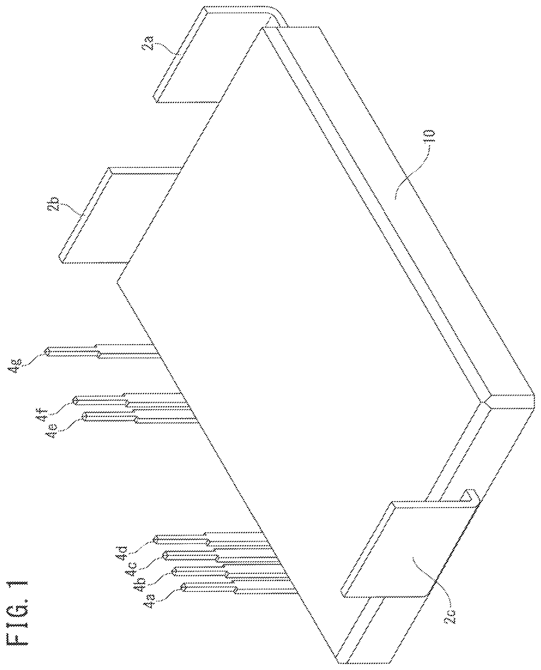
is a perspective view illustrating a semiconductor device (a power semiconductor module) according to a first embodiment, and is a plan view illustrating the semiconductor device according to the first embodiment. As illustrated in and , the semiconductor device according to the first embodiment includes a sealing resin 10 that seals power semiconductor elements (semiconductor chips), an external terminal (a negative electrode terminal) 2 a , an external terminal (a positive electrode terminal) 2 b , an external terminal (an output terminal) 2 c , and control terminals 4 a to 4 g each projecting from the sealing resin 10 .
The sealing resin 10 has a substantially rectangular parallelepiped. The negative electrode terminal 2 a and the positive electrode terminal 2 b project from the common one surface of the substantially rectangular parallelepiped of the sealing resin 10 . The output terminal 2 c projects from another one surface of the substantially rectangular parallelepiped of the sealing resin 10 opposed to the surface from which the negative electrode terminal 2 a and the positive electrode terminal 2 b project. The control terminals 4 a to 4 g project from still another one surface of the substantially rectangular parallelepiped of the sealing resin 10 located between the surface from which the negative electrode terminal 2 a and the positive electrode terminal 2 b project and the surface from which the output terminal 2 c projects.
The sealing resin 10 is made of resin having the insulating properties such as epoxy resin. The output terminal 2 c , the positive electrode terminal 2 b , the negative electrode terminal 2 a , and the control terminals 4 a to 4 g are each made from conductive material such as copper (Cu), a Cu alloy, aluminum (Al), or an Al alloy, for example.
is a perspective view illustrating the semiconductor device according to the first embodiment while omitting the sealing resin 10 illustrated in and . is a plan view corresponding to , is a side view corresponding to , and is an enlarged side view of region A in .
As illustrated in to , the semiconductor device according to the first embodiment includes a conductive substrate 1 a and a conductive substrate 1 b arranged separately from each other. The conductive substrate 1 a and the conductive substrate 1 b each have a substantially rectangular planar pattern. The conductive substrate 1 a and the conductive substrate 1 b are each made from conductive material such as copper (Cu) and aluminum (Al), for example. The respective bottom surfaces of the conductive substrate 1 a and the conductive substrate 1 b are exposed on the sealing resin 10 illustrated in and .
The output terminal 2 c is a flat plate bent into an L-shape, and is bonded to the conductive substrate 1 a by use of bonding material such as solder or sintered material or by direct bonding. The positive electrode terminal 2 b is a flat plate bent into an L-shape, and is bonded to the conductive substrate 1 b by use of bonding material such as solder or sintered material or by direct bonding. The negative electrode terminal 2 a is arranged next to the positive electrode terminal 2 b , and includes an external connection part 24 that is a flat plate bent into an L-shape. The negative electrode terminal 2 a extends toward the output terminal 2 c so as to be elongated across the conductive substrate 1 a and the conductive substrate 1 b.
Although not illustrated in or , a conductive member (also referred to as an “intermediate clip” or a “lead frame”) 6 illustrated in is interposed between the negative electrode terminal 2 a and the respective conductive substrates 1 a and 1 b . The conductive member 6 is arranged to be separately opposed to a part of the negative electrode terminal 2 a . A part of the negative electrode terminal 2 a and a part of the conductive member 6 are covered with a resin member 8 .
The negative electrode terminal 2 a , the conductive member 6 , and the resin member 8 are integrated together by integral molding so as to implement an integrated structure body ( 2 a , 6 , 8 ). The resin member 8 is partly interposed between the negative electrode terminal 2 a and the conductive member 6 . The integration molding of the negative electrode terminal 2 a , the conductive member 6 , and the resin member 8 while keeping a gap between the negative electrode terminal 2 a and the conductive member 6 with the resin member 8 interposed can ensure low inductance and insulation properties, and enables a void management (evaluation). Further, integrating the negative electrode terminal 2 a , the conductive member 6 , and the resin member 8 together as a single component can avoid an increase in cost derived from a complication of jigs or lead frames, and can lead to a decrease in the manufacturing steps. The respective structures of the negative electrode terminal 2 a , the conductive member 6 , and the resin member 8 are described below.
is a perspective view illustrating the semiconductor device according to the first embodiment while omitting the illustration of the sealing resin 10 illustrated in and and further omitting the illustration of the integrated structure body ( 2 a , 6 , 8 ) implemented by the negative electrode terminal 2 a , the conductive member 6 , and the resin member 8 . is a plan view corresponding to .
As illustrated in and , the semiconductor device according to the first embodiment includes a plurality of (six) power semiconductor elements (semiconductor chips) 3 a to 3 f arranged on the top surface side of the conductive substrate 1 a , and a plurality of (six) power semiconductor elements (semiconductor chips) 3 g to 3 l arranged on the top surface side of the conductive substrate 1 b . The semiconductor chips 3 a to 3 f are bonded onto the conductive substrate 1 a by use of bonding material such as solder or sintered material. The semiconductor chips 3 g to 3 l are bonded onto the conductive substrate 1 b by use of bonding material such as solder or sintered material.
The semiconductor device according to the first embodiment is illustrated with a case in which the semiconductor chips 3 a to 3 l are each a MOSFET, and is illustrated with a “2-in-1” power semiconductor module including two sets of the six MOSFETs arranged in parallel, the two sets being arranged in series. The set of the semiconductor chips 3 a to 3 f serves as a lower arm of a half bridge circuit for one phase in a three-phase inverter circuit, and the other set of the semiconductor chips 3 g to 3 l serves as an upper arm. The semiconductor device according to the first embodiment is not limited to the 2-in-1 semiconductor module, and may be a 6-in-1 semiconductor module instead.
The semiconductor chips 3 a to 3 l include semiconductor substrates, first main electrodes (drain electrodes) provided on the bottom surface side of the semiconductor substrate, and second main electrodes (source electrodes) 31 a to 31 l and control electrodes (gate electrodes) provided on the top surface side of the semiconductor substrate. The respective drain electrodes of the semiconductor chips 3 a to 3 f are electrically connected to the conductive substrate 1 a . The respective drain electrodes of the semiconductor chips 3 g to 3 l are electrically connected to the conductive substrate 1 b.
The respective semiconductor substrates of the semiconductor chips 3 a to 3 l include silicon (Si), silicon carbide (SIC), gallium nitride (GaN), or gallium oxide (Ga 2 O 3 ), for example. The arranged positions and the number of the semiconductor chips 3 a to 3 l may be changed as appropriate. The semiconductor chips 3 a to 3 l are each a field effect transistor (FET) such as a MOSFET, or may be an insulated gate bipolar transistor (IGBT), a static induction (SI) thyristor, or a gate turn-off (GTO) thy ristor.
A printed board for control wiring ( 11 , 12 a to 12 e ) is arranged on the conductive substrate 1 a on the top surface side. The printed board for control wiring ( 11 , 12 a to 12 e ) includes an insulating layer 11 , and conductive layers 12 a to 12 e arranged separately from each other on the top surface side of the insulating layer 11 . The insulating layer 11 is made of a ceramic plate mainly including aluminum oxide (Al 2 O 3 ), aluminum nitride (AlN), silicon nitride (SisN 4 ), or boron nitride (BN), or a resin insulating layer including polymer material, for example. The conductive layers 12 a to 12 e each include copper (Cu) or aluminum (Al), for example.
The insulating layer 11 and the conductive layer 12 a extend from the end part of the conductive substrate 1 a along the region between the semiconductor chips 3 a to 3 c and the semiconductor chips 3 d to 3 f . The control terminal 4 a is bonded to the conductive layer 12 a by use of bonding material such as solder or sintered material. The conductive layer 12 a is electrically connected to the respective gate electrodes of the semiconductor chips 3 a to 3 f via control wires (bonding wires) 72 a to 72 f . The control terminal 4 a applies a control signal to the respective gate electrodes of the semiconductor chips 3 a to 3 f through the conductive layer 12 a and the respective bonding wires 72 a to 72 f.
The conductive layer 12 b is provided parallel to the conductive layer 12 a so as to extend from the end part of the conductive substrate 1 along the region between the semiconductor chips 3 a to 3 c and the semiconductor chips 3 d to 3 f . The control terminal 4 b is bonded to the conductive layer 12 b by use of bonding material such as solder or sintered material. The conductive layer 12 b is electrically connected to part of the respective source electrodes 31 a to 31 f of the semiconductor chips 3 a to 3 f via control wires (bonding wires) 71 a to 71 f . The control terminal 4 b detects a current flowing through the respective source electrodes 31 a to 31 l of the semiconductor chips 3 a to 3 f via the respective bonding wires 71 a to 71 f and the conductive layer 12 b.
The control terminal 4 c is bonded to the conductive layer 12 c by use of bonding material such as solder or sintered material. The control terminal 4 d is bonded to the conductive layer 12 d by use of bonding material such as solder or sintered material. A temperature detection chip 5 is bonded to the conductive layer 12 e by use of bonding material such as solder or sintered material. The conductive layer 12 d is connected to the temperature detection chip 5 via a control wire (a bonding wire) 73 . The control terminal 4 d detects a temperature detection signal from the temperature detection chip 5 through the bonding wire 73 and the conductive layer 12 d.
The conductive substrate 1 a is provided with pads 15 a to 15 c at positions on the top surface side adjacent to the conductive substrate 1 b . The respective pads 15 a to 15 c are bonded to the top surface of the conductive substrate 1 a by use of bonding material such as solder or sintered material. The pads 15 a to 15 c are made from conductive material such as copper (Cu) or aluminum (Al), for example. The respective pads 15 a to 15 c may be formed integrally with the conductive substrate 1 a.
The conductive substrate 1 b is provided with a printed board for control wiring ( 13 , 14 a to 14 c ) arranged on the top surface side. The printed board for control wiring ( 13 , 14 a to 14 c ) includes an insulating layer 13 , and conductive layers 14 a to 14 c arranged separately from each other on the top surface side of the insulating layer 13 . The insulating layer 13 can be made from the same material as the insulating layer 11 , and the respective conductive layers 14 a to 14 c can be made from the same material as the conductive layers 12 a to 12 e.
The insulating layer 13 and the conductive layer 14 a are arranged to extend from the end part of the conductive substrate 1 b along the region between the semiconductor chips 3 g to 3 i and the semiconductor chips 3 j to 3 l . The control terminal 4 e is bonded to the conductive layer 14 a by use of bonding material such as solder or sintered material. The conductive layer 14 a is electrically connected to the respective gate electrodes of the semiconductor chips 3 g to 3 l via control wires (bonding wires) 72 g to 72 l . The control terminal 4 e applies a control signal to the respective gate electrodes of the semiconductor chips 3 g to 3 l through the conductive layer 14 a and the bonding wires 72 g to 72 l.
The conductive layer 14 b is arranged to extend parallel to the conductive layer 14 a from the end part of the conductive substrate 1 b along the region between the semiconductor chips 3 g to 3 i and the semiconductor chips 3 j to 3 l . The control terminal 4 f is bonded to the conductive layer 14 b by use of bonding material such as solder or sintered material. The conductive layer 14 b is electrically connected to part of the respective source electrodes 31 g to 31 l of the semiconductor chips 3 g to 3 l via control wires (bonding wires) 71 g to 71 l . The control terminal 4 f detects a current flowing through the respective source electrodes 31 g to 31 l of the semiconductor chips 3 g to 3 l via the bonding wires 71 g to 71 l and the conductive layer 14 b.
The control terminal 4 g is bonded to the conductive layer 14 c by use of bonding material such as solder or sintered material. The conductive layer 14 c is connected to the conductive substrate 1 b via a control wire (a bonding wire) 74 . The control terminal 4 g detects a current flowing through the respective drain electrodes of the semiconductor chips 3 g to 3 l via the bonding wire 74 and the conductive layer 14 c.
is a perspective view illustrating the conductive member 6 implementing one of the constitutional elements of the integrated structure body ( 2 a , 6 , 8 ). As illustrated in , the conductive member 6 incudes pad bonding parts 61 a to 61 c , a connection part 62 connected to the pad bonding parts 61 a to 61 c , chip bonding parts 63 a to 63 c connected to the connection part 62 , connection parts 64 a to 64 c connected to the chip bonding parts 63 a to 63 c , and chip bonding parts 63 d to 6 f connected to the connection parts 64 a to 64 c . The respective pad bonding parts 61 a to 61 c and the respective chip bonding parts 63 a to 63 f are bent to project downward and connected to the connection part 62 and the respective connection parts 64 a to 64 c . The respective connection parts 64 a to 64 c have a stripe-shaped planar pattern extending parallel to and separately from each other.
At least the respective bottom surfaces of the pad bonding parts 61 a to 61 e are exposed on the resin member 8 illustrated in to . The pad bonding parts 61 a to 61 c are bonded to the pads 15 a to 15 c on the top surface side of the conductive substrate 1 a illustrated in and by use of bonding material such as solder or sintered material. The connection part 62 and the respective connection parts 64 a to 64 c are covered with the resin member 8 illustrated in to . At least the respective bottom surfaces of the chip bonding parts 63 a to 63 f are exposed on the resin member 8 illustrated in to . The chip bonding parts 63 a to 63 f are bonded to the source electrodes 31 g to 31 of the semiconductor chips 3 g to 3 l illustrated in and by use of bonding material such as solder or sintered material.
is a perspective view illustrating the negative electrode terminal 2 a implementing one of the constitutional elements of the integrated structure body ( 2 a , 6 . 8 ). As illustrated in , the negative electrode terminal 2 a includes chip bonding parts 21 a to 21 c , connection parts 22 a to 22 c connected to the chip bonding parts 21 a to 21 c , chip bonding parts 21 d to 21 f connected to the connection parts 22 a to 22 c , a connection part 23 connected to the chip bonding parts 21 d to 21 f , and an external connection part 24 connected to the connection part 23 . The chip bonding parts 21 a to 21 f , the connection parts 22 a to 22 c , and the external connection part 24 are exposed on the resin member 8 illustrated in to . The connection part 23 is partly exposed on the resin member 8 illustrated in to , while the other part of the connection part 23 is covered with the resin member 8 .
The respective chip bonding parts 21 a to 21 f illustrated in are bent to project downward and connected to the connection parts 22 a to 22 c . The chip bonding parts 21 a to 21 f are bonded to the source electrodes 31 a to 31 f of the semiconductor chips 3 a to 3 f illustrated in and by use of bonding material such as solder or sintered material. The respective connection parts 22 a to 22 c have a stripe-shaped planar pattern extending parallel to and separately from each other.
The connection part 23 has a substantially rectangular planar pattern. The connection part 23 is arranged to be opposed to the pad bonding parts 61 a to 61 c , the connection part 62 , the chip bonding parts 63 a to 63 f , and the connection parts 64 a to 64 c of the conductive member 6 illustrated in . The connection part 23 is provided with openings 23 a and 23 b penetrating from the top surface to the bottom surface of the connection part 23 . The openings 23 a and 23 b each have a substantially rectangular planar pattern. The opening 23 a is located to overlap with the space between the respective connection parts 64 a and 64 b illustrated in . The opening 23 b is located to overlap with the space between the respective connection parts 64 b and 64 c illustrated in .
The opening 23 a is located to overlap with a control wiring region in a plan view including the bonding wires 71 h , 71 k , 72 h , and 72 k connected to the semiconductor chips 3 h and 3 k illustrated in and . The opening 23 b is located to overlap with a control wiring region including the bonding wires 71 i , 71 l , 72 i , and 72 l connected to the semiconductor chips 3 i and 3 l illustrated in and .
The part of the negative electrode terminal 2 a corresponding to the external connection part 24 may be defined as a “negative electrode terminal”, and the other part including the chip bonding parts 21 a to 21 c , the connection parts 22 a to 22 c , the chip bonding pats 21 d to 21 f , and the connection part 23 other than the extema connection part 24 may be defined as a “lead frame” integrated with the “negative electrode terminal”.
is a perspective view illustrating the resin member 8 implementing one of the constitutional elements of the integrated structure body ( 2 a , 6 , 8 ). As illustrated in , the resin member 8 includes a body part 80 having a substantially rectangular cuboidal outline. The body part 80 is provided on one of the side surfaces with an opening 82 and openings 83 a to 83 c . The connection part 23 of the negative electrode terminal 2 a is partly exposed outward through the opening 82 . The pad bonding parts 61 a to 61 c of the conductive member 6 are exposed outward through the openings 83 a to 83 c respectively. The body part 80 is provided with openings 81 a and 81 b penetrating from the top surface to the bottom surface of the body part 80 . The openings 81 a and 81 b are located to respectively overlap with the openings 23 a and 23 b of the negative electrode terminal 2 a illustrated in .
As illustrated in and , the opening 81 a of the resin member 8 is located to overlap with the control wiring region including the bonding wires 71 h , 71 k . 72 h , and 72 k connected to the semiconductor chips 3 h and 3 k in the plan view when the integrated structure body ( 2 a , 6 , 8 ) is arranged on the top surface side of the respective conductive substrates 1 a and 1 b . The opening 81 b is located to overlap with the control wiring region including the bonding wires 71 i , 711 , 72 i , and 72 l connected to the semiconductor chips 3 i and 3 l.
As illustrated in to , a support part 84 and support parts 85 a to 85 e are provided on the bottom surface side of the body part 80 . schematically indicates the support parts 85 a to 85 e hidden under the body part 80 by the broken lines. The support part 84 and the support parts 85 a to 85 e are formed integrally with the body part 80 . The support part 84 is arranged on the top surface side of the conductive substrate 1 a . The support parts 85 a to 85 e are arranged on the top surface side of the conductive substrate 1 b . The respective support parts 85 a to 85 e are illustrated with a case of having a pillar-like shape, for example, but are not limited to this case. The arranged positions and the number of the support parts 85 a to 85 e may be changed as appropriate.
The provision of the support part 84 and the support parts 85 a to 85 e on the bottom surface side of the body part 80 can suppress an inclination of the integrated structure body ( 2 a , 6 , 8 ) including the chip bonding parts 21 a to 21 f of the negative electrode terminal 2 a and the chip bonding parts 63 a to 63 f of the conductive member 6 so as to avoid an increase in height of the integrated structure body ( 2 a , 6 , 8 ) when the chip bonding parts 21 a to 21 f and the chip bonding parts 63 a to 63 f are bonded by soldering to the respective source electrodes of the semiconductor chips 3 a to 3 l.
The surface of the resin member 8 may be subjected to embossing treatment so as to be roughened. The roughened surface of the resin member 8 can avoid a separation and thus improve the adhesion between the resin member 8 and the sealing resin 10 . Either the entire surface or a part of the surface of the resin member 8 can be subjected to the roughening.
is a schematic side view illustrating a packaged structure of a semiconductor device 101 according to the first embodiment. The semiconductor device 101 corresponds to the semiconductor device illustrated in and , and the respective bottom surfaces of the conductive substrates 1 a and 1 b are exposed on the bottom surface of the semiconductor device 101 . A cooling device (a base) 103 is arranged on the bottom surface side of the semiconductor device 101 with a sheet-like resin layer (a resin sheet) 102 interposed.
The resin sheet 102 is a member for ensuring both the insulation and the adhesion between the semiconductor device 101 and the cooling device 103 while enabling the release of heat from the semiconductor device 101 toward the cooling device 103 . The material used for the resin sheet 102 can be epoxy resin, for example. The material used for the cooling device 103 can be copper (Cu), aluminum (Al), composite material (AISiC) including Al and silicon carbide, or composite material (MgSiC) including magnesium (Mg) and silicon carbide, for example.
The packaged structure of the semiconductor device 101 can integrate the functions of the insulation, the adhesion, and the heat release into the resin sheet 102 , so as to reduce the costs accordingly, as compared with a case in which the insulated circuit substrate is bonded to the cooling device by soldering.
is an equivalent circuit diagram illustrating the semiconductor device according to the first embodiment. As illustrated in , the semiconductor device according to the first embodiment implements a part of a three-phase bridge circuit. A drain electrode of a transistor T 1 on the upper arm side is connected to a positive electrode terminal P, and a source electrode of a transistor T 2 on the lower arm side is connected to a negative electrode terminal N. A source electrode of the transistor T 1 and a drain electrode of the transistor T 2 are connected to an output terminal U and an auxiliary source terminal S 1 . An auxiliary source terminal S 2 is connected to the source electrode of the transistor T 2 . Gate control terminals G 1 and G 2 are connected to the gate electrodes of the transistors T 1 and T 2 . Body diodes D 1 and D 2 each serving as a freewheeling diode (FWD) are internally connected in antiparallel to the transistors T 1 and T 2 .
The output terminal U, the positive electrode terminal P, and the negative electrode terminal N illustrated in respectively correspond to the output terminal 2 c , the positive electrode terminal 2 b , and the negative electrode terminal 2 a illustrated in and . The transistor T 1 and the body diode D 1 illustrated in correspond to the semiconductor chips 3 g and 3 l illustrated in and . The transistor T 2 and the body diode D 2 illustrated in correspond to the semiconductor chips 3 a to 3 f illustrated in and . The gate control terminals G 1 and G 2 illustrated in correspond to the control terminals 4 a and 4 e illustrated in and . The auxiliary source terminals S 1 and S 2 illustrated in correspond to the control terminals 4 b and 4 f illustrated in and .
An example of a method of manufacturing the semiconductor device according to the first embodiment is described below. As illustrated in and , the output terminal 2 c , the semiconductor chips 3 a to 3 f , the printed board ( 11 , 12 a to 12 e ), and the pads 15 a to 15 c are bonded to the top surface of the conductive substrate 1 a by use of bonding material such as solder or sintered material. The control terminals 4 a to 4 d and the temperature detection chip 5 are further bonded to the top surface of the printed board ( 11 , 12 a to 12 e ) by use of bonding material such as solder or sintered material. The semiconductor chips 3 a to 3 f , the printed board ( 11 , 12 a to 12 e ), and the temperature detection chip 5 are then connected to each other via the bonding wires 71 a to 71 f , 72 a to 72 f , and 73 .
As illustrated in and , the positive electrode terminal 2 b , the semiconductor chips 3 g to 3 l , and the printed board ( 13 , 14 a to 14 c ) are bonded to the top surface of the conductive substrate 1 b by use of bonding material such as solder or sintered material. The control terminals 4 e to 4 g are further bonded to the top surface of the printed board ( 13 , 14 a to 14 c ) by use of bonding material such as solder or sintered material. The semiconductor chips 3 g to 3 l and the printed board ( 13 , 14 a to 14 c ) are then connected to each other via the bonding wires 71 g to 71 l and 72 g to 72 l.
The conductive member 6 illustrated in , the negative electrode terminal 2 a illustrated in , and the resin member 8 illustrated in l are formed integrally by integral molding with a metal mold so as to prepare the integrated structure body ( 2 a , 6 , 8 ).
Next, as illustrated in to , the conductive substrate 1 a to which the semiconductor chips 3 a to 3 f and the like are bonded and the conductive substrate 1 b to which the semiconductor chips 3 g to 3 l and the like are bonded are led to be opposed to the integrated structure body ( 2 a . 6 , 8 ). The chip bonding parts 21 a to 21 f of the negative electrode terminal 2 a implementing a part of the integrated structure body ( 2 a , 6 , 8 ) are then bonded to the source electrodes 31 a to 31 f of the semiconductor chips 3 a to 3 f by use of bonding material such as solder or sintered material. Similarly, the chip bonding parts 63 a to 63 f of the conductive member 6 implementing a part of the integrated structure body ( 2 a , 6 , 8 ) are bonded to the source electrodes 31 g to 31 l of the semiconductor chips 3 g to 3 l by use of bonding material such as solder or sintered material. Similarly, the pad bonding parts 61 a to 61 c of the conductive member 6 are bonded to the pads 15 a to 15 c on the top surface side of the conductive substrate 1 a by use of bonding material such as solder or sintered material.
Next, the semiconductor chips 3 a to 3 l and the like are sealed with the sealing resin 10 by transfer molding, as illustrated in . The semiconductor device according to the first embodiment is thus completed.
The semiconductor device according to the first embodiment described above has the integrated structure body ( 2 a , 6 , 8 ) including the negative electrode terminal 2 a , the conductive member 6 , and the resin member 8 integrated together so as to implement a three-dimensionally-wired main wiring circuit, while including the control wiring circuit implemented by the printed board for control wiring ( 11 , 12 a to 12 e ) and the printed board for control wiring ( 13 , 14 a to 14 e ) so as to include the separated substrates.
The semiconductor device according to the first embodiment having the configuration as described above thus can decrease the wiring area, so as to achieve a reduction in chip size and cost and also ensure the low inductance properties, as compared with the conventional semiconductor device in which the semiconductor chips are mounted on the circuit pattern of the insulated circuit substrate so that the semiconductor chips and the circuit pattern of the insulated circuit substrate are electrically connected together via lead frames and bonding wires.
Further, the semiconductor device according to the first embodiment having the configuration as described above can ensue the reliability of the connection parts, so as to facilitate an inspection process to achieve a reduction in cost accordingly, as compared with the conventional semiconductor device in which the printed board is arranged over the semiconductor chips mounted on the insulated circuit substrate so that the semiconductor chips and the printed board are electrically connected together by use of pin terminals. Further, the semiconductor device according to the first embodiment does not have a problem of a cause of any curve or thermal deformation in the printed board, so as to increase the packaging performance and increase the reliability to facilitate the handling accordingly.
Further, the semiconductor device according to the first embodiment having the configuration as described above does not need to use a case, so as to achieve a reduction in space, a decrease in the number of manufacturing steps, and a reduction in cost, as compared with the conventional semiconductor device that uses a case for surrounding the insulated circuit substrate so as to inject resin by potting to seal the insulated circuit substrate.
As described above, the semiconductor device according to the first embodiment can exhibit the wiring technique that contributes to a reduction in cost and facilitate the manufacturing process without requiring a complicated member-positioning accurate control technique, and can further keep the heat-releasing performance and achieve the low inductance performance that can maximize the characteristics of the semiconductor chips including silicon carbide (SiC) and the like. The semiconductor device according to the first embodiment having the configuration as described above is particularly effective for a case in which a plurality of small semiconductor chips including SiC are connected in parallel in order to reduce the manufacturing costs, since this configuration can greatly contribute to a decrease in wiring area if including the plural semiconductor chips.
SECOND EMBODIMENT
A semiconductor device according to a second embodiment has an external appearance similar to that of the semiconductor device according to the first embodiment illustrated in and . is a perspective view illustrating the semiconductor device according to the second embodiment while omitting the sealing resin 10 illustrated in and , and is a plan view corresponding to .
As illustrated in and , the semiconductor device according to the second embodiment differs from the semiconductor device according to the first embodiment in including a resin member 9 arranged to be interposed between the negative electrode terminal 2 a and the conductive member 6 . The semiconductor device according to the second embodiment has a laminated structure body ( 2 a , 6 , 9 ) including the negative electrode terminal 2 a , the conductive member 6 , and the resin member 9 stacked together. The negative electrode terminal 2 a and the conductive member 6 implementing the constitutional elements of the laminated structure body ( 2 a , 6 , 9 ) have the same structure as the negative electrode terminal 2 a illustrated in and the conductive member 6 illustrated in .
is a perspective view illustrating the resin member 9 as one of the constituent elements of the laminated structure body ( 2 a , 6 , 9 ). As illustrated in , the resin member 9 includes a flat part 90 and stripe parts 91 a to 91 c connected to the flat part 90 . The flat part 90 is arranged between the connection part 62 of the conductive member 6 illustrated in and the connection part 23 of the negative electrode terminal 2 a illustrated in . The flat part 90 is provided with a projecting part 94 on the bottom surface side. The projecting part 94 is fitted to the pad bonding parts 61 a to 61 c of the conductive member 6 curved downward illustrated in . The flat part 90 is not necessarily provided with the projecting part 94 .
The stripe part 91 a is interposed between the chip bonding part 63 a , the connection part 64 a , and the chip bonding part 63 d of the conductive member 6 illustrated in and the stripe part of the negative electrode terminal 2 a toward the end part on the outer side of the opening 23 a of the connection part 23 illustrated in . The stripe part 91 a is provided with projecting parts 95 a and 95 d on the bottom surface side. The projecting parts 95 a and 95 d are fitted to the chip bonding parts 63 a and 63 d of the conductive member 6 curved downward illustrated in .
The stripe part 91 b is interposed between the chip bonding part 63 b , the connection part 64 b , and the chip bonding part 63 e of the conductive member 6 illustrated in and the stripe part located between the respective openings 23 a and 23 b of the connection part 23 of the negative electrode terminal 2 a illustrated in . The stripe part 91 b is provided with projecting parts 95 b and 95 e on the bottom surface side. The projecting parts 95 b and 95 e are fitted to the chip bonding parts 63 b and 63 e of the conductive member 6 curved downward illustrated in .
The stripe part 91 c is interposed between the chip bonding part 63 c , the connection part 64 c , and the chip bonding part 63 f of the conductive member 6 illustrated in and the stripe part of the negative electrode terminal 2 a toward the end part on the outer side of the opening 23 b of the connection part 23 illustrated in . The stripe part 91 c is provided with projecting parts 95 c and 95 f on the bottom surface side. The projecting parts 95 c and 95 f are fitted to the chip bonding parts 63 c and 63 f of the conductive member 6 curved downward illustrated in .
The space between the respective stripe parts 91 a and 91 b is defined to overlap with the space between the respective connection parts 64 a and 64 b of the conductive member 6 illustrated in and overlap with the opening 23 a of the connection part 23 of the negative electrode terminal 2 a illustrated in . The space between the respective stripe parts 91 b and 91 c is defined to overlap with the space between the respective connection parts 64 b and 64 c of the conductive member 6 illustrated in and overlap with the opening 23 b of the connection part 23 of the negative electrode terminal 2 a illustrated in .
is a side view illustrating the laminated structure body ( 2 a , 6 , 9 ). As illustrated in , the chip bonding parts 63 c and 63 f of the conductive member 6 on the top surface side are in contact with the projecting parts 95 c and 95 f of the resin member 9 respectively. Similarly, the chip bonding parts 63 a , 63 b , 63 d , and 63 e of the conductive member 6 on the top surface side are in contact with the projecting parts 95 a , 95 b . 95 d , and 95 e of the resin member 9 respectively. As illustrated in , the flat part 90 and the stripe part 91 c of the resin member 9 on the top surface side are in contact with the bottom surface of the connection part 23 of the negative electrode terminal 2 a . Similarly, the respective stripe parts 91 a and 91 b of the resin member 9 on the top surface side are in contact with the bottom surface of the connection part 23 of the negative electrode terminal 2 a.
is an enlarged side view of region A surrounded by the broken line illustrating the circumference of the projecting part 95 c of the resin member 9 in . The side surface of the projecting part 95 c of the resin member 9 is provided with engagement parts (protruding parts) 92 a and 92 b . The curved part of the projecting part 63 c of the conductive member 6 is provided with engagement parts (recessed parts) 65 a and 65 b . The protruding parts 92 a and 92 b of the resin member 9 and the recessed parts 65 a and 65 b of the conductive member 6 are engaged (fitted) together, so as to fix the conductive member 6 and the resin member 9 to each other.
is a view illustrating an example of a method of assembling the laminated structure body ( 2 a , 6 , 9 ) illustrated in . First, the negative electrode terminal 2 a , the resin member 9 , and the conductive member 6 are prepared, and the top surface of the resin member 9 is bonded (fixed) to the bottom surface of the negative electrode terminal 2 a by pressure bonding, for example, as illustrated in . Next, the top surface of the conductive member 6 is opposed to the bottom surface of the resin member 9 fixed to the negative electrode terminal 2 a so as to be fixed together by pressure bonding, for example. At this point, the protruding parts 92 a and 92 b of the resin member 9 and the recessed parts 65 a and 65 b of the conductive member 6 are engaged (fitted) together, so as to stably fix the top surface of the conductive member 6 to the bottom surface of the resin member 9 .
The other configurations of the semiconductor device according to the second embodiment are substantially the same as the semiconductor device according to the first embodiment, and overlapping explanations are not repeated below.
The semiconductor device according to the second embodiment has the laminated structure body ( 2 a , 6 , 9 ) including the negative electrode terminal 2 a , the conductive member 6 , and the resin member 9 integrated together so as to implement the three-dimensionally-wired main wiring circuit, while including the control wiring circuit implemented by the printed board for control wiring ( 11 , 12 a to 12 e ) and the printed board for control wiring ( 13 , 14 a to 14 e ) so as to include the separated substrates. This configuration can decrease the wiring area, so as to avoid an increase in chip size and cost, ensuring the low inductance properties accordingly.
is a perspective view illustrating another example of the conductive member 6 implementing one of the constituent elements of the laminated structure body ( 2 a , 6 , 9 ). The conductive member 6 illustrated in differs from the conductive member 6 illustrated in in further having a connection part 65 connected to the chip bonding parts 63 d to 63 f . is a perspective view illustrating another example of the resin member 9 implementing one of the constituent elements of the laminated structure body ( 2 a , 6 , 9 ). The resin member 9 illustrated in differs from the resin member 9 illustrated in in further having a connection part 97 connected to the stripe parts 91 a to 91 c . The semiconductor device according to the second embodiment may include the laminated structure body ( 2 a , 6 , 9 ) implemented by the conductive member 6 illustrated in , the resin member 9 illustrated in , and the negative electrode terminal 2 a illustrated in .
OTHER EMBODIMENTS
While the present invention has been described above by reference to the first and second embodiments, it should be understood that the present invention is not intended to be limited to the descriptions and the drawings composing part of this disclosure. Various alternative embodiments, examples, and technical applications will be apparent to those skilled in the art according to this disclosure.
For example, the first and second embodiments have been illustrated with the case of including the conductive substrate 1 a and the conductive substrate 1 b , but the present invention may also be applied to a case of using a circuit pattern on the upper surface side of an insulated circuit substrate such as a direct copper bonded (DCB) substrate for the conductive substrate 1 a and the conductive substrate 1 b.
Further, the configurations disclosed in the first and second embodiments may be combined as appropriate within a range that does not contradict with the scope of the respective embodiments. As described above, the invention includes various embodiments of the present invention and the like not described herein. Therefore, the scope of the present invention is defined only by the technical features specifying the present invention, which are prescribed by claims, the words and terms in the claims shall be reasonably construed from the subject matters recited in the present specification.
Figures (18)
Citations
This patent cites (20)
- US11328985
- US11664298
- US2003/0168252
- US2016/0148859
- US2016/0293563
- US2019/0057921
- US2021/0066256
- US2021/0098347
- US2021/0308791
- US2021/0313256
- US2022/0238475
- US2022/0246507
- US2022/0254696
- US2023/0326907
- US2023/0352376
- US2006-086438
- US2013-051295
- US2021-009973
- US2019/239771
- US2020/045263