Abstract
A semiconductor device includes an output circuit and a switching element. The output circuit includes a switching element, a sense switching element, and a shunt breaking circuit. When an upper arm side switching element changes from an on-state to an off-state, a regenerative current flows from a load because of the regenerative operation of the load. In the output circuit, the shunt breaking circuit is located on the low potential side of a sense MOSFET in the sense switching element. As a result, a shunt of the regenerative current, which is generated at the time of the regenerative operation of the load, to the sense switching element is cut off by the shunt breaking circuit.
Claims (20)
1 . A semiconductor device, comprising: a lower arm circuit including a lower arm side output circuit including: a lower arm side switching element that is switching-controlled by a lower arm side control circuit and that supplies a power to a load; a lower arm side current monitoring element that is switching-controlled by the lower arm side control circuit and that monitors a current flowing through the lower arm side switching element; and a lower arm side shunt breaking circuit that is a circuit element that, without application of a control signal, always blocks current in one direction and allows current to pass in the opposite direction, the lower side shunt breaking circuit being electrically connected to a low potential side terminal of the lower arm side current monitoring element; and an upper arm side switching element connected in series with the lower arm side switching element, wherein the lower arm side shunt breaking circuit cuts off a shunt of a regenerative current flowing from the load to the lower arm side current monitoring element upon the upper arm side switching element changing from an on-state to an off-state, the load being connected to a connection point of the upper arm side switching element and the lower arm side switching element at one side thereof, and connected to a low potential side terminal of the lower arm side switching element at another side thereof.
11 . A semiconductor device, comprising: an upper arm circuit including an upper arm side output circuit including: an upper arm side switching element that is switching-controlled by an upper arm side control circuit and that supplies a power to a load; an upper arm side current monitoring element that is switching-controlled by the upper arm side control circuit and that monitors a current flowing through the upper arm side switching element; and an upper arm side shunt breaking circuit that is a circuit element that, without application of a control signal, always blocks current in one direction and allows current to pass in the opposite direction, the lower side shunt breaking circuit being electrically connected to a low potential side terminal of the upper arm side current monitoring element; and a lower arm side switching element connected in series with the upper arm side switching element, wherein the upper arm side shunt breaking circuit cuts off a shunt of a regenerative current flowing from the load to the upper arm side current monitoring element upon the lower arm side switching element changing from an on-state to an off-state, the load being connected to a high potential side terminal of the upper arm side switching element at a first end thereof, and connected to a connection point of the lower arm side switching element and the upper arm side switching element at a second end thereof.
Show 18 dependent claims
2 . The semiconductor device according to claim 1 , wherein the lower arm circuit further includes a sense resistor that converts a sense current output from the lower arm side current monitoring element to a voltage signal.
3 . The semiconductor device according to claim 2 , wherein: the lower arm circuit further includes the lower arm side control circuit; and the lower arm side control circuit further includes a current detection circuit that detects a current state of the lower arm side switching element by comparing the voltage signal with a threshold voltage.
4 . The semiconductor device according to claim 3 , wherein the lower arm side shunt breaking circuit is located between the low potential side terminal of the lower arm side current monitoring element and a high potential side terminal of the sense resistor.
5 . The semiconductor device according to claim 4 , wherein: the upper arm side switching element is an upper arm side main metal oxide-semiconductor field-effect transistor (MOSFET) having an upper built-in diode therein; the lower arm side switching element is a lower arm side main MOSFET having a first lower built-in diode therein; the lower arm side current monitoring element is a sense MOSFET having a second lower built-in diode therein; the circuit element forming the lower arm side shunt breaking circuit is another diode; a drain of the lower arm side main MOSFET is connected to a cathode of the first lower built-in diode, a drain of the sense MOSFET, a cathode of the second lower built-in diode and the connection point; the connection point is connected to a source of the upper arm side main MOSFET; an anode of the another diode is connected to a source of the sense MOSFET and an anode of the second lower built-in diode; a cathode of the another diode is connected to the high potential side terminal of the sense resistor and an input end of the current detection circuit; and a low potential side terminal of the sense resistor is connected to a source of the lower arm side main MOSFET and an anode of the first lower built-in diode.
6 . The semiconductor device according to claim 5 , wherein: the current detection circuit detects the lower arm side main MOSFET being in an overcurrent state upon detection of the voltage signal being greater than or equal to the threshold voltage, the voltage signal being generated on a basis of a voltage drop that occurs as a result of the sense current output from the sense MOSFET and flowing through the sense resistor; and the lower arm side control circuit stops driving the lower arm side main MOSFET upon detection of the lower arm side main MOSFET being in the overcurrent state.
7 . The semiconductor device according to claim 3 , wherein the lower arm side shunt breaking circuit is located between the low potential side terminal of the lower arm side switching element and a low potential side terminal of the sense resistor.
8 . The semiconductor device according to claim 7 , wherein: the upper arm side switching element is an upper arm side main MOSFET having an upper built-in diode therein; the lower arm side switching element is a lower arm side main MOSFET having a first lower built-in diode therein; the lower arm side current monitoring element is a sense MOSFET having a second lower built-in diode therein; the lower arm side shunt breaking circuit is another diode; a drain of the lower arm side main MOSFET is connected to a cathode of the first lower built-in diode, a drain of the sense MOSFET, a cathode of the second lower built-in diode and the connection point, the connection point is connected to a source of the upper arm side main MOSFET; a high potential side terminal of the sense resistor is connected to an input end of the current detection circuit, a source of the sense MOSFET and an anode of the second lower built-in diode; an anode of the another diode is connected to the low potential side terminal of the sense resistor; and a cathode of the another diode is connected to a source of the lower arm side main MOSFET and an anode of the first lower built-in diode.
9 . The semiconductor device according to claim 8 , wherein: the current detection circuit detects that the lower arm side main MOSFET is in an overcurrent state upon detection of the voltage signal being greater than or equal to the threshold voltage, the voltage signal being generated on a basis of a voltage drop that occurs as a result of the sense current being output from the sense MOSFET and flowing through the sense resistor, and a forward voltage drop that occurs as a result of the sense current flowing through the another diode; and the lower arm side control circuit stops driving the lower arm side main MOSFET upon detection of the lower arm side main MOSFET being in the overcurrent state.
10 . The semiconductor device according to claim 1 , further comprising a printed-circuit board on which the lower arm side output circuit is disposed, wherein the lower arm side shunt breaking circuit is located on the printed-circuit board, or inside the lower arm side control circuit.
12 . The semiconductor device according to claim 11 , wherein the upper arm circuit further includes a sense resistor that converts a sense current output from the upper arm side current monitoring element to a voltage signal.
13 . The semiconductor device according to claim 12 , wherein: the upper arm circuit further includes the upper arm side control circuit; and the upper arm side control circuit further includes a current detection circuit that detects a current state of the upper arm side switching element by comparing the voltage signal with a threshold voltage.
14 . The semiconductor device according to claim 13 , wherein the upper arm side shunt breaking circuit is located between the low potential side terminal of the upper arm side current monitoring element and a high potential side terminal of the sense resistor.
15 . The semiconductor device according to claim 14 , wherein: the lower arm side switching element is a lower arm side main MOSFET having a lower built-in diode therein; the upper arm side switching element is an upper arm side main MOSFET having a first upper built-in diode therein; the upper arm side current monitoring element is a sense MOSFET having a second upper built-in diode therein; the upper arm side shunt breaking circuit is another diode; a drain of the upper arm side main MOSFET is connected to a cathode of the first upper built-in diode, a drain of the sense MOSFET, a cathode of the second upper built-in diode and the first end of the load; an anode of the another diode is connected to a source of the sense MOSFET and an anode of the second upper built-in diode; a cathode of the another diode is connected to the high potential side terminal of the sense resistor and an input end of the current detection circuit; a low potential side terminal of the sense resistor is connected via the connection point to a source of the upper arm side main MOSFET, an anode of the first upper built-in diode and the second end of the load; and the connection point is connected to a drain of the lower arm side main MOSFET.
16 . The semiconductor device according to claim 15 , wherein: the current detection circuit detects the upper arm side main MOSFET being in an overcurrent state upon detection of the voltage signal being greater than or equal to the threshold voltage, the voltage signal being generated on a basis of a voltage drop that occurs as a result of the sense current being output from the sense MOSFET and flowing through the sense resistor is greater than or equal to the threshold voltage; and the upper arm side control circuit stops driving the upper arm side main MOSFET upon detection of the upper arm side main MOSFET being in the overcurrent state.
17 . The semiconductor device according to claim 13 , wherein the upper arm side shunt breaking circuit is located between a low potential side terminal of the upper arm side switching element and a low potential side terminal of the sense resistor.
18 . The semiconductor device according to claim 17 , wherein: the lower arm side switching element is a lower arm side main MOSFET having a lower built-in diode therein; the upper arm side switching element is an upper arm side main MOSFET having a first upper built-in diode therein; the upper arm side current monitoring element is a sense MOSFET having a second upper built-in diode therein; the upper arm side shunt breaking circuit is another diode; a drain of the upper arm side main MOSFET is connected to a cathode of the first upper built-in diode, a drain of the sense MOSFET, a cathode of the second upper built-in diode and the first end of the load; a high potential side terminal of the sense resistor is connected to an input end of the current detection circuit, a source of the sense MOSFET and an anode of the second upper built-in diode; an anode of the another diode is connected to the low potential side terminal of the sense resistor; a cathode of the another diode is connected via the connection point to a source of the upper arm side main MOSFET, an anode of the first upper built-in diode and the second end of the load; and the connection point is connected to a drain of the lower arm side main MOSFET.
19 . The semiconductor device according to claim 18 , wherein: the current detection circuit detects the upper arm side main MOSFET being in an overcurrent state upon detection of the voltage signal being greater than or equal to the threshold voltage, the voltage signal being generated on a basis of a voltage drop that occurs as a result of the sense current being output from the sense MOSFET and flowing through the sense resistor, and a forward voltage drop that occurs as a result of the sense current flowing through the another diode; and the upper arm side control circuit stops driving the upper arm side main MOSFET upon detection of the upper arm side main MOSFET being in the overcurrent state.
20 . The semiconductor device according to claim 11 , further including a printed-circuit board on which the upper arm side output circuit is disposed, wherein the upper arm side shunt breaking circuit is located on the printed-circuit board or inside the upper arm side control circuit.
Full Description
Show full text →
CROSS-REFERENCE TO RELATED APPLICATION
This application is based upon and claims the benefit of priority of the prior Japanese Patent Application No. 2023-010427, filed on Jan. 26, 2023, the entire contents of which are incorporated herein by reference.
BACKGROUND OF THE INVENTION
1. Field of the Invention
The embodiment discussed herein relates to a semiconductor device.
2. Background of the Related Art
Silicon-insulated gate bipolar transistors (Si-IGBTs), which are silicon (Si)-element IGBTs, have been used in power modules of semiconductor devices. In recent years, however, there has been a growing tendency to use silicon carbide-metal oxide-semiconductor field-effect transistors (SiC-MOSFETs), which are silicon carbide (SiC)-element MOSFETs, in place of Si-element IGBTs.
Such an SiC-MOSFET has a high dielectric breakdown field strength, compared with an IGBT. Accordingly, such an SiC-MOSFET has a high breakdown voltage. Furthermore, with such an SiC-MOSFET, it is possible to make impurity concentration higher and make an active layer thinner. This leads to high efficiency and high-speed switching operation. As a result, it is expected that power dissipation is reduced.
On the other hand, semiconductor devices in which an SiC-MOSFET is used as a main switch are applied to power converters, such as three-phase inverters which supply power to a load such as a motor. Furthermore, when the load is in a short-circuit state, there is a possibility that an excessive current larger than current flowing at normal operation time flows and that a failure occurs in the main switch or a peripheral circuit. Accordingly, a sense switch is located as one of fault tolerant design for a semiconductor device for detecting overcurrent.
For example, the following technique was proposed as a related art. When a reverse overcurrent detection circuit detects reverse overcurrent, control is exercised so as to turn on a main switching element and a sense switching element (see, for example, Japanese Patent No. 5717915).
A built-in diode is attached to a switching element using an SiC-MOSFET. With a semiconductor device in which such an SiC-MOSFET is used in a main switch and a sense switch, it is assumed that a regenerative current is generated in a load. Then part of the regenerative current flows into the inside of a control IC which drives the main switch and the sense switch, and a reverse voltage is generated in the control IC.
is a view for describing the generation of a reverse voltage caused by a shunt of a regenerative current. A semiconductor device 100 includes an upper arm circuit 114 , a lower arm circuit 124 , and a load L connected to one another via a node n. The lower arm circuit 124 has an output circuit 120 and a control IC 121 . The output circuit 120 includes a main switch sw 1 b and a sense switch sw 2 b . The upper arm circuit 114 includes the same components that the lower arm circuit 124 includes.
The main switch sw 1 b which operates the load L has a main MOSFET 1 b 1 . Furthermore, the main switch sw 1 b has a built-in diode Db 1 connected in inverse parallel with the main MOSFET 1 b 1 . Similarly, the sense switch sw 2 b which detects sense current has a sense MOSFET 1 b 2 . Furthermore, the sense switch sw 2 b has a built-in diode Db 2 connected in inverse parallel with the sense MOSFET 1 b 2 . An SiC-MOSFET is used as the main MOSFET 1 b 1 and the sense MOSFET 1 b 2 .
In the output circuit 120 , a drain of the main MOSFET 1 b 1 is connected to a cathode of the built-in diode Db 1 , a drain of the sense MOSFET 1 b 2 , a cathode of the built-in diode Db 2 , and the node n. The node n is connected to a current output terminal of a switching element (not illustrated) in the upper arm circuit 114 and one end of the load L.
A gate of the main MOSFET 1 b 1 is connected to a gate of the sense MOSFET 1 b 2 and an output terminal OUT of the control IC 121 . A source of the sense MOSFET 1 b 2 is connected to an anode of the built-in diode Db 2 and is connected via an input terminal IN of the control IC 121 to one end of a sense resistor Rs. The other end of the sense resistor Rs is connected to a source of the main MOSFET 1 b 1 , an anode of the built-in diode Db 1 , and the other end of the load L.
The main switch sw 1 b and the sense switch sw 2 b are switching-driven by a drive signal ds output from the output terminal OUT of the control IC 121 . Furthermore, the control IC 121 receives at the input terminal IN a sense current Is flowing from the sense switch sw 2 b and converts the sense current Is into a voltage signal by the sense resistor Rs. In addition, on the basis of the voltage signal, the control IC 121 detects at a subsequent stage overcurrent which may occur in the main switch sw 1 b.
When a switching element (not illustrated) located in an output circuit of the upper arm circuit 114 changes from an on-state to an off-state in the semiconductor device 100 having the above structure, a regenerative current IF is generated in the load L because of the regenerative operation of the load L. Furthermore, part of the regenerative current IF flows via the diode Db 2 attached to the sense switch sw 2 b . If an IGBT is used as a switching element, then part of the regenerative current IF does not flow via a built-in diode because an IGBT does not have a built-in diode.
With the semiconductor device 100 having the above structure, however, a MOSFET is used in the sense switch sw 2 b . As a result, part of the regenerative current IF generated at the time of the regenerative operation flows via the built-in diode Db 2 attached to the sense switch sw 2 b.
In this case, as illustrated in , a shunt current I 0 , which is part of the regenerative current IF, is input to the inside of the control IC 121 which drives the sense MOSFET 1 b 2 . As a result, a reverse voltage VR is generated inside the control IC 121 . The reverse breakdown voltage of the control IC 121 is low. Accordingly, when the reverse voltage VR is generated, there is a risk that the control IC 121 fails.
The generation of a reverse voltage in the control IC 121 included in the lower arm circuit 124 has been described. However, a reverse voltage may be generated in the same way in a control IC included in the upper arm circuit 114 due to a shunt of a regenerative current.
SUMMARY OF THE INVENTION
According to an aspect, there is provided a semiconductor device, including: a lower arm circuit including a lower arm side output circuit including: a lower arm side switching element that is switching-controlled by a lower arm side control circuit and that supplies a power to a load; a lower arm side current monitoring element that is switching-controlled by the lower arm side control circuit and that monitors a current flowing through the lower arm side switching element; and a lower arm side shunt breaking circuit electrically connected to a low potential side terminal of the lower arm side current monitoring element; and an upper arm side switching element connected in series with the lower arm side switching element, wherein the lower arm side shunt breaking circuit cuts off a shunt of a regenerative current flowing from the load to the lower arm side current monitoring element upon the upper arm side switching element changing from an on-state to an off-state, the load being connected to a connection point of the upper arm side switching element and the lower arm side switching element at one side thereof, and connected to a low potential side terminal of the lower arm side switching element at another side thereof.
The object and advantages of the invention will be realized and attained by means of the elements and combinations particularly pointed out in the claims.
It is to be understood that both the foregoing general description and the following detailed description are exemplary and explanatory and are not restrictive of the invention.
BRIEF DESCRIPTION OF THE DRAWINGS
is a view for describing an example of a semiconductor device;
illustrates an example of the structure of a semiconductor device;
illustrates an example of the structure of a semiconductor device;
illustrates an example of the structure of a semiconductor device;
illustrates an example of the structure of a semiconductor device;
illustrates an example of the structure of a current detection circuit;
illustrates an example of the structure of a semiconductor device;
illustrates an example of the structure of a semiconductor device;
illustrates an example of the structure of a semiconductor device;
illustrates an example of the structure of a semiconductor device;
illustrates an example of the structure of a current detection circuit;
illustrates the relationship between a main current and a regenerative current;
illustrates the relationship between a regenerative current and a reverse voltage obtained when a reverse-current prevention diode is not located;
illustrates the relationship between a regenerative current and a reverse voltage obtained when a reverse-current prevention diode is located;
illustrates an example of the structure of a power converter; and
is a view for describing the generation of a reverse voltage caused by a shunt of a regenerative current.
DETAILED DESCRIPTION OF THE INVENTION
An embodiment will now be described with reference to the accompanying drawings. Components in the specification and the drawings having substantially the same function are marked with the same reference numeral. By doing so, a duplicate description may be omitted.
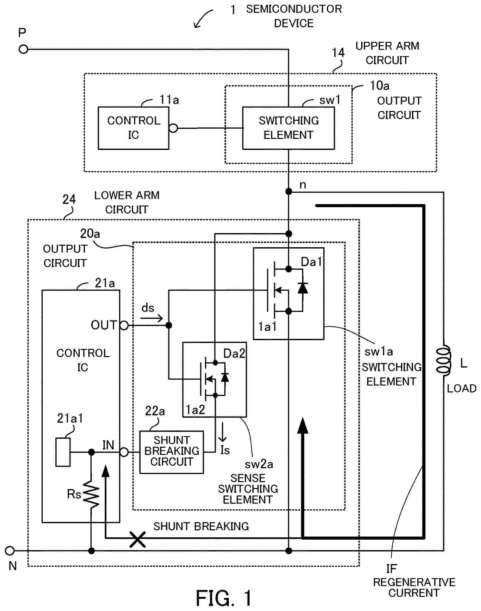
is a view for describing an example of a semiconductor device. A semiconductor device 1 includes an upper arm circuit 14 , a lower arm circuit 24 , and a load L. The upper arm circuit 14 includes an output circuit 10 a (upper arm side output circuit) and a control IC 11 a (upper arm side control circuit). The lower arm circuit 24 includes an output circuit 20 a (lower arm side output circuit) and a control IC 21 a (lower arm side control circuit). Furthermore, the upper arm circuit 14 and the lower arm circuit 24 are connected to the upper arm side and the lower arm side, respectively, via a node n.
The output circuit 10 a includes a switching element sw 1 (upper arm side switching element). The output circuit 20 a includes a switching element sw 1 a (lower arm side switching element), a sense switching element sw 2 a (lower arm side current monitoring element), and a shunt breaking circuit 22 a . Furthermore, the control IC 21 a includes a sense resistor Rs and a current detection circuit 21 a 1 .
The switching element sw 1 a which operates the load L has a main MOSFET 1 a 1 and a built-in diode Da 1 connected in inverse parallel with the main MOSFET 1 a 1 is attached. Similarly, the sense switching element sw 2 a which detects a sense current has a sense MOSFET 1 a 2 and a built-in diode Da 2 connected in inverse parallel with the sense MOSFET 1 a 2 is attached. An SiC-MOSFET is used as the main MOSFET 1 a 1 and the sense MOSFET 1 a 2 .
In the output circuit 20 a , a drain of the main MOSFET 1 a 1 is connected to a cathode of the built-in diode Da 1 , a drain of the sense MOSFET 1 a 2 , a cathode of the built-in diode Da 2 , and the node n. The node n is connected to a current output terminal (low potential side terminal) of a switching element sw 1 and one end (high potential side terminal) of the load L.
A gate of the main MOSFET 1 a 1 is connected to a gate of the sense MOSFET 1 a 2 and an output terminal OUT of the control IC 21 a . A source (low potential side terminal) of the sense MOSFET 1 a 2 is connected to an anode of the built-in diode Da 2 and one terminal of the shunt breaking circuit 22 a . The other terminal of the shunt breaking circuit 22 a is connected via an input terminal IN of the control IC 21 a to an input end of the current detection circuit 21 a 1 and one end of a sense resistor Rs. The other end of a sense resistor Rs is connected to a source of the main MOSFET 1 a 1 , an anode of the built-in diode Da 1 , and the other end of the load L.
The main MOSFET 1 a 1 and the sense MOSFET 1 a 2 are switching-driven by a drive signal ds output from the output terminal OUT of the control IC 21 a . Furthermore, the control IC 21 a receives at the input terminal IN a sense current Is flowing from the sense MOSFET 1 a 2 and converts the sense current Is to a voltage signal by the sense resistor Rs for sense current detection. In addition, on the basis of the voltage signal, the current detection circuit 21 a 1 detects overcurrent which may occur in the main MOSFET 1 a 1 .
When the switching element sw 1 located in the upper arm side output circuit 10 a changes from an on-state to an off-state in the semiconductor device 1 having the above structure, a regenerative current IF is generated in the load L because of the regenerative operation of the load L.
In the output circuit 20 a , the shunt breaking circuit 22 a is located between the sense MOSFET 1 a 2 and the sense resistor Rs. Accordingly, in this case, a shunt of the regenerative current IF, which is generated at the time of the regenerative operation of the load L, to the sense MOSFET 1 a 2 is cut off by the shunt breaking circuit 22 a.
That is to say, a shunt of the regenerative current IF does not occur and the regenerative current IF flows only along a regular route (flow from the load L in a forward direction of the built-in diode Da 1 ). As a result, generation of a reverse voltage caused by a shunt of the regenerative current IF is prevented. This prevents a reverse voltage from being applied to the control IC 21 a.
The structure and operation of a concrete example of the semiconductor device 1 will now be described in detail. In the following description, it is assumed that an SiC-MOSFET is used as a MOSFET.
illustrates an example of the structure of a semiconductor device. A semiconductor device 1 - 1 includes an upper arm circuit 14 , a lower arm circuit 24 , a load L, a capacitor C 1 (polarized), a capacitor C 2 , and a power supply section V DC . The upper arm circuit 14 and the lower arm circuit 24 are located on the upper arm side and the lower arm side, respectively, and are connected via a node n. Furthermore, the load L is an inductive load, for example. One end (first end) of the load L is connected to the node n and the other end (second end) of the load L is connected to a negative electrode side terminal of the power supply section V DC .
The upper arm circuit 14 includes an output circuit 10 and a control IC 13 . The output circuit 10 includes a main switch sw 11 , a sense switch sw 12 , and a reverse-current prevention diode D 1 . The reverse-current prevention diode D 1 corresponds to an upper arm side shunt breaking circuit. The main switch sw 11 has a main MOSFET 11 and a built-in diode (first upper built-in diode) D 11 connected in inverse parallel with the main MOSFET 11 is attached.
Similarly, the sense switch sw 12 which detects a sense current has a sense MOSFET 12 and a built-in diode (second upper built-in diode) D 12 connected in inverse parallel with the sense MOSFET 12 is attached. Furthermore, the control IC 13 includes a sense resistor Rs 1 and a current detection circuit 3 a.
The lower arm circuit 24 includes an output circuit 20 and a control IC 23 . The output circuit 20 includes a main switch sw 21 , a sense switch sw 22 , and a reverse-current prevention diode D 2 . The reverse-current prevention diode D 2 corresponds to a lower arm side shunt breaking circuit. The main switch sw 21 has a main MOSFET 21 and a built-in diode (first lower built-in diode) D 21 connected in inverse parallel with the main MOSFET 21 is attached.
Similarly, the sense switch sw 22 which detects a sense current has a sense MOSFET 22 and a built-in diode (second lower built-in diode) D 22 connected in inverse parallel with the sense MOSFET 22 is attached. Furthermore, the control IC 23 includes a sense resistor Rs 2 and a current detection circuit 3 b.
Each component is connected in the following way. A positive electrode side terminal of the power supply section V DC is connected to one end of the capacitor C 1 , one end of the capacitor C 2 , a drain of the main MOSFET 11 , a cathode of the built-in diode D 11 , a drain of the sense MOSFET 12 , and a cathode of the built-in diode D 12 .
A gate of the main MOSFET 11 is connected to a gate of the sense MOSFET 12 and an output terminal OUT of the control IC 13 . A source of the sense MOSFET 12 is connected to an anode of the built-in diode D 12 and an anode of the reverse-current prevention diode D 1 .
A cathode of the reverse-current prevention diode D 1 is connected via an input terminal IN of the control IC 13 to one end of the sense resistor Rs 1 and an input end of the current detection circuit 3 a . The other end of the sense resistor Rs 1 is connected via the node n to a drain of the main MOSFET 21 , a cathode of the built-in diode D 21 , a drain of the sense MOSFET 22 , a cathode of the built-in diode D 22 , and one end of the load L.
A gate of the main MOSFET 21 is connected to a gate of the sense MOSFET 22 and an output terminal OUT of the control IC 23 . A source of the sense MOSFET 22 is connected to an anode of the built-in diode D 22 and an anode of the reverse-current prevention diode D 2 .
A cathode of the reverse-current prevention diode D 2 is connected via an input terminal IN of the control IC 23 to one end of the sense resistor Rs 2 and an input end of the current detection circuit 3 b . The negative electrode side terminal of the power supply section V DC is connected to the other end of the capacitor C 1 , the other end of the capacitor C 2 , the other end of the sense resistor Rs 2 , a source of the main MOSFET 21 , an anode of the built-in diode D 21 , and the other end of the load L.
In the upper arm circuit 14 , the main switch sw 1 l and the sense switch sw 12 are switching-driven by a drive signal ds 1 output from the output terminal OUT of the control IC 13 .
Furthermore, the control IC 13 receives at the input terminal IN a sense current Is 1 flowing from the sense switch sw 12 and converts the sense current Is 1 to a voltage signal by the sense resistor Rs 1 for sense current detection. In addition, on the basis of the voltage signal, the current detection circuit 3 a detects overcurrent which may occur in the main switch sw 11 .
Furthermore, in the lower arm circuit 24 , the main switch sw 21 and the sense switch sw 22 are switching-driven by a drive signal ds 2 output from the output terminal OUT of the control IC 23 .
In addition, the control IC 23 receives at the input terminal IN a sense current Is 2 flowing from the sense switch sw 22 and converts the sense current Is 2 to a voltage signal by the sense resistor Rs 2 for sense current detection. Moreover, on the basis of the voltage signal, the current detection circuit 3 b detects overcurrent which may occur in the main switch sw 21 .
When the main switch sw 11 located in the output circuit 10 of the upper arm circuit 14 changes from an on-state to an off-state in the semiconductor device 1 - 1 having the above structure, a regenerative current IF is generated in the load L because of the regenerative operation of the load L.
In the output circuit 20 of the lower arm circuit 24 , the reverse-current prevention diode D 2 is located between the sense MOSFET 22 and the sense resistor Rs 2 . Accordingly, in this case, a shunt of the regenerative current IF, which is generated at the time of the regenerative operation of the load L, to the sense MOSFET 22 is cut off by the reverse-current prevention diode D 2 . That is to say, a shunt of the regenerative current IF does not occur. As a result, generation of a reverse voltage caused by a shunt of the regenerative current IF is prevented. This prevents a reverse voltage from being applied to the control IC 23 .
illustrates an example of the structure of a semiconductor device. A semiconductor device 1 - 2 includes an upper arm circuit 14 , a lower arm circuit 24 , a load L, a capacitor C 1 (polarized), a capacitor C 2 , and a power supply section V DC . The upper arm circuit 14 and the lower arm circuit 24 are located on the upper arm side and the lower arm side, respectively, and are connected via a node n. A method for connecting each component in differs from the method for connecting each component in only in that one end of the load L is connected to a positive electrode side terminal of the power supply section V DC and in that the other end of the load L is connected to the node n.
When a main switch sw 21 located in a lower arm side output circuit 20 changes from an on-state to an off-state in the semiconductor device 1 - 2 having the above structure, a regenerative current IF is generated in the load L because of the regenerative operation of the load L.
In an output circuit 10 , a reverse-current prevention diode D 1 is located between a sense MOSFET 12 and a sense resistor Rs 1 . Accordingly, in this case, a shunt of the regenerative current IF, which is generated at the time of the regenerative operation of the load L, to the sense MOSFET 12 is cut off by the reverse-current prevention diode D 1 . That is to say, a shunt of the regenerative current IF does not occur. As a result, generation of a reverse voltage caused by a shunt of the regenerative current IF is prevented. This prevents a reverse voltage from being applied to a control IC 13 .
Each of illustrates an example of the structure of a semiconductor device. With the semiconductor devices 1 - 1 and 1 - 2 illustrated in , respectively, the reverse-current prevention diode D 1 is located over a printed-circuit board of the upper arm circuit 14 outside the control IC 13 and the reverse-current prevention diode D 2 is located over a printed-circuit board of the lower arm circuit 24 outside the control IC 23 .
With semiconductor devices 1 - 1 a and 1 - 2 a illustrated in , respectively, on the other hand, a control IC 13 a includes a sense resistor Rs 1 , a current detection circuit 3 a , and a reverse-current prevention diode D 1 and a control IC 23 a includes a sense resistor Rs 2 , a current detection circuit 3 b , and a reverse-current prevention diode D 2 .
A reverse-current prevention diode may be located in this way in a control IC for integration. By adopting such structure, circuit mounting scale over a printed-circuit board of an upper arm circuit 14 and a printed-circuit board of a lower arm circuit 24 is reduced.
illustrates an example of the structure of a current detection circuit. A “current detection circuit 3 ” is a general term for the current detection circuits 3 a and 3 b included in the control ICs 13 and 23 , respectively, and a “sense resistor Rs” is a general term for the sense resistors Rs 1 and Rs 2 included in the control ICs 13 and 23 , respectively.
The current detection circuit 3 includes a comparator cmp 1 . One end of the sense resistor Rs is connected to a non-inverting input terminal (+) of the comparator cmp 1 and a threshold voltage Voc is applied to an inverting input terminal (−) of the comparator cmp 1 . The other end of the sense resistor Rs is connected to GND.
When a main MOSFET is turned on, on the basis of a drive signal, a sense MOSFET is also turned on and a sense current Is is output from a source of the sense MOSFET. Furthermore, the sense current Is output from the sense MOSFET flows through a sense resistor Rs. As a result, a drop in voltage occurs and a voltage signal Vs (=Rs×Is) generated at this time is input to a current detection circuit 3 .
The comparator cmp 1 of the current detection circuit 3 compares the voltage signal Vs and a threshold voltage Voc to detect whether or not the main MOSFET is in an overcurrent state. When the voltage signal Vs is higher than or equal to the threshold voltage Voc (Voc≤Vs), the comparator cmp 1 outputs an H-level overcurrent detection signal s 1 . When a control IC 13 recognizes the overcurrent detection signal s 1 , the control IC 13 stops driving the main MOSFET.
illustrates an example of the structure of a semiconductor device. A semiconductor device 1 - 1 b includes an upper arm circuit 14 , a lower arm circuit 24 , a load L, a capacitor C 1 (polarized), a capacitor C 2 , and a power supply section V DC . The upper arm circuit 14 and the lower arm circuit 24 are located on the upper arm side and the lower arm side, respectively, and are connected via a node n. One end of the load L is connected to the node n and the other end of the load L is connected to a negative electrode side terminal of the power supply section V DC .
Furthermore, a reverse-current prevention diode D 1 is located between a sense resistor Rs 1 and a current output terminal of a main switch sw 11 and a reverse-current prevention diode D 2 is located between a sense resistor Rs 2 and a current output terminal of a main switch sw 21 .
That is to say, an anode of the reverse-current prevention diode D 1 is connected to the other end of the sense resistor Rs 1 . A cathode of the reverse-current prevention diode D 1 is connected to a source of a main MOSFET 11 and an anode of a built-in diode D 11 and is connected via the node n to the one end of the load L.
On the other hand, an anode of the reverse-current prevention diode D 2 is connected to the other end of the sense resistor Rs 2 . A cathode of the reverse-current prevention diode D 2 is connected to a source of a main MOSFET 21 , an anode of a built-in diode D 21 , and the other end of the load L. A method for connecting each component in differs from the method for connecting each component in only in these respects.
When the main switch sw 11 located in an output circuit 10 of the upper arm circuit 14 changes from an on-state to an off-state in the semiconductor device 1 - 1 b having the above structure, a regenerative current IF is generated in the load L because of the regenerative operation of the load L.
The reverse-current prevention diode D 2 is located between the sense resistor Rs 2 and the current output terminal of the main switch sw 21 in an output circuit 20 of the lower arm circuit 24 . Accordingly, in this case, a shunt of the regenerative current IF, which is generated at the time of the regenerative operation of the load L, to the sense switch sw 22 is cut off by the reverse-current prevention diode D 2 . That is to say, a shunt of the regenerative current IF does not occur. As a result, application of a reverse voltage caused by a shunt of the regenerative current IF to the control IC 23 is prevented.
illustrates an example of the structure of a semiconductor device. A semiconductor device 1 - 2 b includes an upper arm circuit 14 , a lower arm circuit 24 , a load L, a capacitor C 1 (polarized), a capacitor C 2 , and a power supply section V DC . The upper arm circuit 14 and the lower arm circuit 24 are located on the upper arm side and the lower arm side, respectively, and are connected via a node n. One end of the load L is connected to a positive electrode side terminal of the power supply section V DC and the other end of the load L is connected to the node n. A method for connecting each component in differs from the method for connecting each component in only in this respect.
When a main switch sw 21 located in an output circuit 20 of the lower arm circuit 24 changes from an on-state to an off-state in the semiconductor device 1 - 2 b having the above structure, a regenerative current IF is generated in the load L because of the regenerative operation of the load L.
A reverse-current prevention diode D 1 is located between a sense resistor Rs 1 and a current output terminal of a main switch sw 11 in an output circuit 10 of the upper arm circuit 14 . Accordingly, in this case, a shunt of the regenerative current IF, which is generated at the time of the regenerative operation of the load L, to a sense switch sw 12 is cut off by the reverse-current prevention diode D 1 . That is to say, a shunt of the regenerative current IF does not occur. As a result, application of a reverse voltage caused by a shunt of the regenerative current IF to the control IC 13 is prevented.
Each of illustrates an example of the structure of a semiconductor device. With the semiconductor devices 1 - 1 b and 1 - 2 b illustrated in , respectively, the reverse-current prevention diode D 1 is located over a printed-circuit board of the upper arm circuit 14 outside the control IC 13 and the reverse-current prevention diode D 2 is located over a printed-circuit board of the lower arm circuit 24 outside the control IC 23 .
With semiconductor devices 1 - 1 c and 1 - 2 c illustrated in , respectively, on the other hand, a control IC 13 c includes a sense resistor Rs 1 , a current detection circuit 3 a , and a reverse-current prevention diode D 1 and a control IC 23 c includes a sense resistor Rs 2 , a current detection circuit 3 b , and a reverse-current prevention diode D 2 .
A reverse-current prevention diode may be located in this way in a control IC for integration. By adopting such structure, circuit mounting scales over a printed-circuit board of an upper arm circuit 14 and a printed-circuit board of a lower arm circuit 24 are reduced.
illustrates an example of the structure of a current detection circuit. A current detection circuit 3 includes a comparator cmp 1 . One end of a sense resistor Rs is connected to a non-inverting input terminal (+) of the comparator cmp 1 and a threshold voltage Voc 1 is applied to an inverting input terminal (−) of the comparator cmp 1 . An anode of a reverse-current prevention diode D 0 is connected to the other end of the sense resistor Rs and a cathode of the reverse-current prevention diode D 0 is connected to GND.
When a main MOSFET is turned on, on the basis of a drive signal, a sense MOSFET is also turned on and a sense current Is is output from a sense source of the sense MOSFET. Furthermore, the sense current Is output from the sense MOSFET flows through a sense resistor Rs and the reverse-current prevention diode D 0 .
When the sense current Is flows through the sense resistor Rs, a voltage drop (Rs×Is) occurs. When the sense current Is flows through the reverse-current prevention diode D 0 , a forward voltage drop (Vf) occurs. That is to say, a voltage drop corresponding to the total of these voltage drops occurs. As a result, a voltage signal Vs 1 (=Rs×Is+Vf) is input to the comparator cmp 1 .
The comparator cmp 1 of the current detection circuit 3 compares the voltage signal Vs 1 and a threshold voltage Voc 1 to detect whether or not the main MOSFET is in an overcurrent state. When the voltage signal Vs 1 is higher than or equal to the threshold voltage Voc 1 (Voc 1 ≤Vs 1 ), the comparator cmp 1 outputs an H-level overcurrent detection signal s 1 . When a control IC recognizes the overcurrent detection signal s 1 , the control IC stops driving the main MOSFET.
Simulation results will now be described with reference to through 14 . illustrates the relationship between a main current and a regenerative current. In , a vertical axis indicates current and a horizontal axis indicates time.
(time t 1 ) An upper arm main MOSFET 11 is turned on. At this time, a main current (drain current) id of the main MOSFET 11 begins to flow and the main current id increases.
(time t 2 ) The upper arm main MOSFET 11 is turned off. At this time, the main current id of the main MOSFET 11 drops and the flow of the main current id decreases. Furthermore, because the main MOSFET 11 changes from an on-state to an off-state, a load L performs regenerative operation, a regenerative current IF begins to flow, and the regenerative current IF increases.
(time t 2 to time t 3 ) For a time period from the time t 2 at which the main MOSFET 11 is turned off to the time t 3 at which the main MOSFET 11 is turned on, the load L performs the regenerative operation and the regenerative current IF flows.
(time t 3 ) The upper arm main MOSFET 11 is turned on. At this time, the main current id of the main MOSFET 11 begins to flow and the main current id increases. Furthermore, the flow of the regenerative current IF decreases.
(time t 4 ) The upper arm main MOSFET 11 is turned off. At this time, the main current id of the main MOSFET 11 drops and the flow of the main current id decreases. Furthermore, because the main MOSFET 11 changes from an on-state to an off-state, the load L performs regenerative operation, the regenerative current IF begins to flow, and the regenerative current IF increases. The amount of the regenerative current IF increases in proportion to the amount of the main current id.
illustrates the relationship between a regenerative current and a reverse voltage obtained when a reverse-current prevention diode is not located. In , a vertical axis indicates current or voltage and a horizontal axis indicates time.
(time t 11 ) An upper arm main MOSFET 11 is turned on.
(time t 12 ) The upper arm main MOSFET 11 is turned off. Because the main MOSFET 11 changes from an on-state to an off-state, a load L performs regenerative operation, a regenerative current IF begins to flow, and the regenerative current IF increases. Furthermore, because part of the regenerative current IF flows to a control IC, a reverse voltage VR is generated in the control IC. In the example of , the reverse voltage VR of about 2.6 volts is generated in the control IC.
(time t 12 to time t 13 ) For a time period from the time t 12 at which the main MOSFET 11 is turned off to the time t 13 at which the main MOSFET 11 is turned on, the regenerative current IF flows. Accordingly, the reverse voltage VR is generated in the control IC for this time period.
(time t 13 ) The upper arm main MOSFET 11 is turned on. The regenerative operation is stopped and the flow of the regenerative current IF decreases. Accordingly, the generation of the reverse voltage VR is also stopped.
(time t 14 ) The upper arm main MOSFET 11 is turned off. Because the main MOSFET 11 changes from an on-state to an off-state, the load L performs regenerative operation, the regenerative current IF begins to flow, and the regenerative current IF increases. Furthermore, because part of the regenerative current IF flows to the control IC, the reverse voltage VR is generated again in the control IC.
illustrates the relationship between a regenerative current and a reverse voltage obtained when a reverse-current prevention diode is located. In , a vertical axis indicates current or voltage and a horizontal axis indicates time.
(time t 21 ) An upper arm main MOSFET 11 is turned on.
(time t 22 ) The upper arm main MOSFET 11 is turned off. Because the main MOSFET 11 changes from an on-state to an off-state, a load L performs regenerative operation, a regenerative current IF begins to flow, and the regenerative current IF increases. Furthermore, because a reverse-current prevention diode is located, a shunt of the regenerative current IF to a control IC is cut off and a reverse voltage VR is not generated in the control IC.
(time t 22 to time t 23 ) For a time period from the time t 22 at which the main MOSFET 11 is turned off to the time t 23 at which the main MOSFET 11 is turned on, the regenerative current IF flows. However, because the reverse-current prevention diode is located, a shunt of the regenerative current IF to the control IC is cut off and the reverse voltage VR is not generated in the control IC.
(time t 23 ) The upper arm main MOSFET 11 is turned on. The regenerative operation is stopped and the flow of the regenerative current IF decreases.
(time t 24 ) The upper arm main MOSFET 11 is turned off. Because the main MOSFET 11 changes from an on-state to an off-state, the load L performs regenerative operation, the regenerative current IF begins to flow, and the regenerative current IF increases. However, because the reverse-current prevention diode is located, a shunt of the regenerative current IF to the control IC is cut off and the reverse voltage VR is not generated in the control IC. By adopting the structure according to the present disclosure, the generation of the reverse voltage VR is prevented in this way.
A power converter to which the semiconductor device according to the present disclosure is applied will now be described. illustrates an example of the structure of a power converter. A power converter 4 includes switching elements sw 41 , sw 42 , and sw 43 for a U phase, a V phase, and a W phase, respectively, located on an upper arm side and switching elements sw 44 , sw 45 , and sw 46 for an X phase, a Y phase, and a Z phase, respectively, located on a lower arm side.
Furthermore, the power converter 4 includes an alternating-current power supply V AC , a rectifying device 47 , a smoothing capacitor C 0 , a controller 40 , and a load M. The rectifying device 47 converts an alternating-current voltage output from the alternating-current power supply V AC to a direct-current voltage V DC 0 .
On the other hand, power is supplied to the load M from a wiring 4 a connected to a node n 1 , which is a connection point of the switching element sw 41 and the switching element sw 44 , a wiring 4 b connected to a node n 2 , which is a connection point of the switching element sw 42 and the switching element sw 45 , and a wiring 4 c connected to a node n 3 , which is a connection point of the switching element sw 43 and the switching element sw 46 .
The U-phase switching element sw 41 includes a main MOSFET 4 u and a built-in diode Du. The V-phase switching element sw 42 includes a main MOSFET 4 v and a built-in diode Dv. The W-phase switching element sw 43 includes a main MOSFET 4 w and a built-in diode Dw.
The X-phase switching element sw 44 includes a main MOSFET 4 x and a built-in diode Dx. The Y-phase switching element sw 45 includes a main MOSFET 4 y and a built-in diode Dy. The Z-phase switching element sw 46 includes a main MOSFET 4 z and a built-in diode Dz.
Furthermore, control circuits 41 , 42 , and 43 which exercise drive control or the like of the switching elements sw 41 , sw 42 , and sw 43 , respectively, are located. Control circuits 44 , 45 , and 46 which exercise drive control or the like of the switching elements sw 44 , sw 45 , and sw 46 , respectively, are located. In addition, the controller 40 which exercises batch control of the control circuits 41 through 46 is located. For example, each of the control circuits 41 , 42 , and 43 has the structure (except the main switch sw 11 ) and function of the upper arm circuit 14 . For example, each of the control circuits 44 , 45 , and 46 has the structure (except the main switch sw 21 ) and function of the lower arm circuit 24 .
Each component is connected in the following way. A positive electrode side terminal of the rectifying device 47 is connected to one end of the smoothing capacitor C 0 , a drain of the main MOSFET 4 u , a cathode of the built-in diode Du, a drain of the main MOSFET 4 v , a cathode of the built-in diode Dv, a drain of the main MOSFET 4 w , and a cathode of the built-in diode Dw.
A negative electrode side terminal of the rectifying device 47 is connected to the other end of the smoothing capacitor C 0 , a source of the main MOSFET 4 x , an anode of the built-in diode Dx, a source of the main MOSFET 4 y , an anode of the built-in diode Dy, a source of the main MOSFET 4 z , and an anode of the built-in diode Dz.
A gate of the main MOSFET 4 u is connected to the control circuit 41 . An anode of the built-in diode Du is connected to a source of the main MOSFET 4 u , the control circuit 41 , and the node n 1 . The node n 1 is connected to the load M, a drain of the main MOSFET 4 x , and a cathode of the built-in diode Dx.
A gate of the main MOSFET 4 v is connected to the control circuit 42 . An anode of the built-in diode Dv is connected to a source of the main MOSFET 4 v , the control circuit 42 , and the node n 2 . The node n 2 is connected to the load M, a drain of the main MOSFET 4 y , and a cathode of the built-in diode Dy.
A gate of the main MOSFET 4 w is connected to the control circuit 43 . An anode of the built-in diode Dw is connected to a source of the main MOSFET 4 w , the control circuit 43 , and the node n 3 . The node n 3 is connected to the load M, a drain of the main MOSFET 4 z , and a cathode of the built-in diode Dz.
The controller 40 controls the control circuit 41 by a control signal Vin-u, controls the control circuit 42 by a control signal Vin-v, and controls the control circuit 43 by a control signal Vin-w. Similarly, the controller 40 controls the control circuit 44 by a control signal Vin-x, controls the control circuit 45 by a control signal Vin-y, and controls the control circuit 46 by a control signal Vin-z.
As described above, a semiconductor device according to the present disclosure includes a shunt breaking circuit. As a result, a shunt of a regenerative current, which is generated at the time of the regenerative operation of a load, to a control IC is suppressed. This suppresses generation of heat by the control IC caused by a shunt current and prevents a failure of the control IC caused by generation of a reverse voltage.
The embodiments have been taken as an example. The structure of each section indicated in each embodiment may be replaced by another structure having the same function. Furthermore, any other component or process may be added. Moreover, the structures (features) of any two or more of the above embodiments may be combined.
According to an aspect, a shunt of a regenerative current is suppressed and generation of a reverse voltage is prevented.
All examples and conditional language provided herein are intended for the pedagogical purposes of aiding the reader in understanding the invention and the concepts contributed by the inventor to further the art, and are not to be construed as limitations to such specifically recited examples and conditions, nor does the organization of such examples in the specification relate to a showing of the superiority and inferiority of the invention. Although one or more embodiments of the present invention have been described in detail, it should be understood that various changes, substitutions, and alterations could be made hereto without departing from the spirit and scope of the invention.
Figures (16)
Citations
This patent cites (4)
- US2014/0321012
- US2016/0011266
- US2018/0206359
- US5717915