Method for Driving Display Panel, and Display Apparatus
Abstract
A method for driving a display panel, and a display apparatus. An example of the method includes: receiving display data of an image to be displayed of the current display frame; and according to the display data, controlling a display panel to sequentially load a gate-on signal to gate lines, and to input a voltage into a data line, and when there is an overlap time between gate-on signals loaded to M adjacent gate lines, a pre-charging voltage and a compensation voltage are sequentially charged to a sub-pixel electrically connected to an Mth gate line among the M gate lines within the overlap time, M being an integer and M≥2.
Claims (15)
1 . A method for driving a display panel, comprising: receiving display data of an image to be displayed in a current display frame; and controlling the display panel to apply a gate-on signal to gate lines in sequence, and input a voltage to data lines according to the display data; wherein in response to gate-on signals loaded on adjacent M gate lines having an overlapping time, during the overlapping time, a pre-charge voltage and a compensation voltage are charged to an sub-pixel electrically connected to an Mth gate line of the M gate lines in sequence; wherein M is an integer and M≥2; wherein the compensation voltage is triggered by a set edge of a compensation trigger signal to be input to the data line connected to a corresponding sub-pixel; wherein the set edge of the compensation trigger signal is one of a rising edge and a falling edge, and the set edge of the compensation trigger signal is within the overlapping time; wherein there is a first interval duration between the set edge and a starting moment of the overlapping time, and the first interval duration is not less than 1/2A; and there is a second interval duration between the set edge and an ending moment of the overlapping time, and the second interval duration is not greater than 1/2A; wherein A represents a maintenance duration of the overlapping time.
12 . A display apparatus, comprising: a display panel; and a timing controller, configured to receive display data of an image to be displayed in a current display frame; and control the display panel to apply a gate-on signal to gate lines in sequence and input a voltage to data lines according to the display data; wherein in response to gate-on signals loaded on adjacent M gate lines having an overlapping time, during the overlapping time, a pre-charge voltage and a compensation voltage are charged to an sub-pixel electrically connected to an Mth gate line of the M gate lines in sequence; wherein M is an integer and M≥2; wherein the compensation voltage is triggered by a set edge of a compensation trigger signal to be input to the data line connected to a corresponding sub-pixel; wherein the set edge of the compensation trigger signal is one of a rising edge and a falling edge, and the set edge of the compensation trigger signal is within the overlapping time; wherein there is a first interval duration between the set edge and a starting moment of the overlapping time, and the first interval duration is not less than 1/2A; and there is a second interval duration between the set edge and an ending moment of the overlapping time, and the second interval duration is not greater than 1/2A; wherein A represents a maintenance duration of the overlapping time.
Show 13 dependent claims
2 . The method according to claim 1 , further comprising: in response to the gate-on signals loaded on adjacent M gate lines having the overlapping time, after the overlapping time and during a time when the gate-on signal is applied to the Mth gate line, charging the sub-pixel electrically connected to the Mth gate line with a target voltage corresponding to the display data.
3 . The method according to claim 2 , wherein the display panel comprises a plurality of sub-pixels of different colors, and the display data of the image to be displayed comprises: display data corresponding to each of the plurality of sub-pixels in a one-to-one manner; wherein in response to a grayscale value of the display data corresponding to each sub-pixel being a same grayscale value, the pre-charge voltage, the compensation voltage and the target voltage are same.
4 . The method according to claim 3 , wherein the display panel comprises display sub-pixels and dummy sub-pixels, the display sub-pixels are in a display area, and the dummy sub-pixels are in a non-display area surrounding the display area; and a grayscale value of a target voltage corresponding to the dummy sub-pixel adjacent to the display sub-pixel is same as a grayscale value of a target voltage corresponding to the display sub-pixel.
5 . The method according to claim 2 , wherein the display panel comprises a plurality of sub-pixels of different colors, and the display data of the image to be displayed comprises: display data corresponding to each of the plurality of sub-pixels in a one-to-one manner; wherein in response to grayscale values of the display data corresponding to at least two sub-pixels being different grayscale values, the pre-charge voltage and the compensation voltage are different.
6 . The method according to claim 5 , wherein for a same sub-pixel, a relationship between the pre-charge voltage VY1, the compensation voltage VB1 and the target voltage VM1 which are charged to the sub-pixel is: VM1≤VB1<VY1.
7 . The method according to claim 5 , wherein for a same sub-pixel, a relationship between the pre-charge voltage VY2, the compensation voltage VB2 and the target voltage VM2 which are charged to the sub-pixel is: VY2<VB2≤VM2.
8 . The method according to claim 6 , wherein the display panel comprises display sub-pixels and dummy sub-pixels, the display sub-pixels are in a display area, and the dummy sub-pixels are in a non-display area surrounding the display area; a grayscale value of a target voltage corresponding to the dummy sub-pixel adjacent to the display sub-pixel is same as a grayscale value of a target voltage corresponding to the display sub-pixel; and a compensation voltage of the display sub-pixel adjacent to the dummy sub-pixel is same as the target voltage.
9 . The method according to claim 7 , wherein the controlling of the display panel to apply the gate-on signal to the gate lines in sequence, and input the voltage to the data lines according to the display data, comprises: for sub-pixels electrically connected to a same data line, there is a grayscale value difference between a grayscale value of the display data corresponding to the sub-pixel connected to the Mth gate line and a grayscale value of the display data corresponding to the sub-pixel connected to an (M−1)th gate line; determining whether the grayscale value difference is not less than a grayscale value difference threshold; and in response to the grayscale value difference not being less than the grayscale value difference threshold, during the overlapping time, after the sub-pixel electrically connected to the Mth gate line among the M gate lines is charged with the pre-charge voltage, inputting the compensation voltage to the data line electrically connected to the sub-pixel.
10 . The method according to claim 1 , wherein the target voltage is triggered by a set edge of a target trigger signal to be input to the data line connected to a corresponding sub-pixel; wherein the set edge of the target trigger signal is one of a rising edge and a falling edge; wherein the set edge of the target trigger signal is aligned with the ending moment of the overlapping time or the set edge of the target trigger signal is after the ending moment of the overlapping time.
11 . The method according to claim 10 , wherein the compensation voltage is the target voltage, and the set edge of the compensation trigger signal is the set edge of the target trigger signal that triggers the target voltage.
13 . The display apparatus according to claim 12 , wherein the timing controller comprises a brightness correction module, configured to determine an input time of the compensation voltage and the compensation voltage according to the display data.
14 . The display apparatus according to claim 12 , wherein the display panel comprises: a plurality of sub-pixels; wherein the plurality of sub-pixels are divided into a plurality of sub-pixel groups; and each of the plurality of sub-pixel groups comprises two adjacent sub-pixels in a same row; a plurality of gate lines; wherein each sub-pixel row corresponds to two gate lines; one sub-pixel in each sub-pixel group is electrically connected to one of corresponding two gate lines, and the other sub-pixel in each sub-pixel group is electrically connected to the other one of the corresponding two gate lines; and a plurality of data lines; wherein a column of sub-pixel groups are arranged between every two adjacent data lines; and for two adjacent data lines, one data line is electrically connected to odd-numbered rows of a column of sub-pixel groups arranged between the two adjacent data lines, and the other data line is electrically connected to even-numbered rows of the column of sub-pixel groups arranged between the two adjacent data lines.
15 . The display apparatus according to claim 12 , wherein the plurality of sub-pixels comprise display sub-pixels and dummy sub-pixels; wherein the dummy sub-pixels are in a peripheral area of the display sub-pixels.
Full Description
Show full text →
CROSS-REFERENCE TO RELATED APPLICATIONS
The disclosure is a National Stage of International Application No. PCT/CN2021/131298, filed on Nov. 17, 2021, which is hereby incorporated by reference in its entirety.
TECHNICAL FIELD
The present disclosure relates to the field of display technology, and in particular, to a method for driving a display panel and a display apparatus.
BACKGROUND
A display such as a liquid crystal display (LCD) generally includes a plurality of pixels. Each pixel may include: a red sub-pixel, a green sub-pixel and a blue sub-pixel. By controlling the display data corresponding to each sub-pixel, the display brightness of each sub-pixel is controlled, so as to display the color image by mixing the required displayed colors.
SUMMARY
Embodiments of the present disclosure provide a method for driving a display panel, including:
•
• receiving display data of an image to be displayed in a current display frame; and • controlling the display panel to apply a gate-on signal to gate lines in sequence, and input a voltage to data lines according to the display data; • wherein in response to gate-on signals loaded on adjacent M gate lines having an overlapping time, during the overlapping time, a pre-charge voltage and a compensation voltage are charged to an sub-pixel electrically connected to an Mth gate line of the M gate lines in sequence; wherein M is an integer and M≥2.
In some embodiments, the method further includes: in response to the gate-on signals loaded on adjacent M gate lines having an overlapping time, after the overlapping time and during a time when the gate-on signal is applied to the Mth gate line, charging the sub-pixel electrically connected to the Mth gate line with a target voltage corresponding to the display data.
In some embodiments, the display panel includes display sub-pixels and dummy sub-pixels, the display sub-pixels are in a display area, and the dummy sub-pixels are in a non-display area surrounding the display area; and a grayscale value of a target voltage corresponding to the dummy sub-pixel adjacent to the display sub-pixel is the same as a grayscale value of a target voltage corresponding to the display sub-pixel.
In some embodiments, the display panel includes a plurality of sub-pixels of different colors, and the display data of the image to be displayed includes: display data corresponding to each sub-pixel in a one-to-one manner; and in response to a grayscale value of the display data corresponding to each sub-pixel being the same grayscale value, the pre-charge voltage, the compensation voltage and the target voltage are the same.
In some embodiments, the display panel includes a plurality of sub-pixels of different colors, and the display data of the image to be displayed includes: display data corresponding to each of the plurality of sub-pixels in a one-to-one manner; and in response to grayscale values of the display data corresponding to at least two sub-pixels being different grayscale values, the pre-charge voltage and the compensation voltage are different.
In some embodiments, for a same sub-pixel, a relationship between the pre-charge voltage VY1, the compensation voltage VB1 and the target voltage VM1 which are charged to the sub-pixel is: VM1≤VB1<VY1.
In some embodiments, for a same sub-pixel, a relationship between the pre-charge voltage VY2, the compensation voltage VB2 and the target voltage VM2 which are charged to the sub-pixel is: VY2<VB2≤VM2.
In some embodiments, the display panel includes display sub-pixels and dummy sub-pixels, the display sub-pixels are in a display area, and the dummy sub-pixels are in a non-display area surrounding the display area; a grayscale value of a target voltage corresponding to the dummy sub-pixel adjacent to the display sub-pixel is same as a grayscale value of a target voltage corresponding to the display sub-pixel; and a compensation voltage of the display sub-pixel adjacent to the dummy sub-pixel is same as the target voltage.
In some embodiments, the controlling of the display panel to apply the gate-on signal to the gate lines in sequence, and input the voltage to the data lines according to the display data, includes:
•
• for sub-pixels electrically connected to a same data line, there is a grayscale value difference between a grayscale value of the display data corresponding to the sub-pixel connected to the Mth gate line and a grayscale value of the display data corresponding to the sub-pixel connected to an (M−1)th gate line; • determining whether the grayscale value difference is not less than a grayscale value difference threshold; and • in response to the grayscale value difference not being less than the grayscale value difference threshold, during the overlapping time, after the sub-pixel electrically connected to the Mth gate line among the M gate lines is charged with the pre-charge voltage, inputting the compensation voltage to the data line electrically connected to the sub-pixel.
In some embodiments, the compensation voltage is triggered by a set edge of a compensation trigger signal to be input to the data line connected to a corresponding sub-pixel; and the set edge of the compensation trigger signal is one of a rising edge and a falling edge; and the set edge of the compensation trigger signal is within the overlapping time.
In some embodiments, there is a first interval duration between the set edge and a starting moment of the overlapping time, and the first interval duration is not less than 1/2 A; and
•
• there is a second interval duration between the set edge and an ending moment of the overlapping time, and the second interval duration is not greater than 1/2 A; • wherein A represents a maintenance duration of the overlapping time.
In some embodiments, the target voltage is triggered by a set edge of the target trigger signal to be input to the data line connected to a corresponding sub-pixel; wherein the set edge of the target trigger signal is one of a rising edge and a falling edge; and
•
• the set edge of the target trigger signal is aligned with the ending moment of the overlapping time or the set edge of the target trigger signal is after the ending moment of the overlapping time.
In some embodiments, the compensation voltage is the target voltage, and the set edge of the compensation trigger signal is the set edge of the target trigger signal that triggers the target voltage.
Embodiments of the present disclosure provide a display apparatus, including:
•
• a display panel; and • a timing controller, configured to receive display data of an image to be displayed in a current display frame; and control the display panel to apply a gate-on signal to gate lines in sequence and input a voltage to data lines according to the display data; wherein in response to gate-on signals loaded on adjacent M gate lines having an overlapping time, during the overlapping time, a pre-charge voltage and a compensation voltage are charged to an sub-pixel electrically connected to an Mth gate line of the M gate lines in sequence; wherein M is an integer and M≥2.
In some embodiments, the timing controller includes a brightness correction module, configured to determine an input time of the compensation voltage and the compensation voltage according to the display data.
In some embodiments, the display panel includes:
•
• a plurality of sub-pixels; wherein the plurality of sub-pixels are divided into a plurality of sub-pixel groups; and each of the sub-pixel groups includes two adjacent sub-pixels in a same row; • a plurality of gate lines; wherein each sub-pixel row corresponds to two gate lines; one sub-pixel in each of the sub-pixel groups is electrically connected to one of corresponding two gate lines, and the other sub-pixel in each of the sub-pixel groups is electrically connected to the other one of the corresponding two gate lines; and • a plurality of data lines; wherein a column of sub-pixel groups are arranged between every two adjacent data lines; and for two adjacent data lines, one data line is electrically connected to odd-numbered rows of a column of sub-pixel groups arranged between the two adjacent data lines, and the other data line is electrically connected to even-numbered rows of the column of sub-pixel groups arranged between the two adjacent data lines.
In some embodiments, the plurality of sub-pixels include display sub-pixels and dummy sub-pixels; wherein the dummy sub-pixels are in a peripheral area of the display sub-pixels.
BRIEF DESCRIPTION OF FIGURES
is some structural schematic diagrams of a display apparatus provided by an embodiment of the present disclosure.
is another schematic structural diagram of a display apparatus provided by an embodiment of the present disclosure.
is yet another structural schematic diagram of a display apparatus provided by an embodiment of the present disclosure.
is some timing diagrams of signals provided by an embodiment of the present disclosure.
is some flowcharts of a driving method provided by the embodiment of the present disclosure.
A is some timing diagrams of signals provided by an embodiment of the present disclosure.
B is another timing diagram of signals provided by an embodiment of the present disclosure.
C is yet another timing diagram of signals provided by an embodiment of the present disclosure.
is a schematic diagram of a timing controller, a gate driving circuit and a source driving circuit provided by an embodiment of the present disclosure.
is another timing diagram of signals provided by an embodiment of the present disclosure.
A is some schematic diagrams of a simulation provided by an embodiment of the present disclosure.
B is another schematic diagram of a simulation provided by the embodiments of the present disclosure.
is another timing diagram of signals provided by the embodiment of the present disclosure.
DETAILED DESCRIPTION
In order to make the purpose, technical solutions and advantages of the embodiments of the present disclosure clearer, the following will clearly and completely describe the technical solutions of the embodiments of the present disclosure in conjunction with the accompanying drawings of the embodiments of the present disclosure. Apparently, the described embodiments are some of the embodiments of the present disclosure, not all of them. And in the case of no conflict, the embodiments in the present disclosure and the features in the embodiments can be combined with each other. Based on the described embodiments of the present disclosure, all other embodiments obtained by a person of ordinary skill in the art without creative effort fall within the protection scope of the present disclosure.
Unless otherwise defined, the technical terms or scientific terms used in the present disclosure shall have the usual meanings understood by those skilled in the art to which the present disclosure belongs. “First”, “second” and similar words used in the present disclosure do not indicate any order, quantity or importance, but are only used to distinguish different components. “Comprising” or “including” and similar words mean that the elements or items appearing before the word include the elements or items listed after the word and their equivalents, without excluding other elements or items. Words such as “connected” or “connecting” are not limited to physical or mechanical connections, but may include electrical connections, whether direct or indirect.
It should be noted that the size and shape of each figure in the drawings do not reflect the actual scale, but are only intended to schematically illustrate the content of the present invention. And the same or similar reference numerals represent the same or similar elements or elements having the same or similar functions throughout.
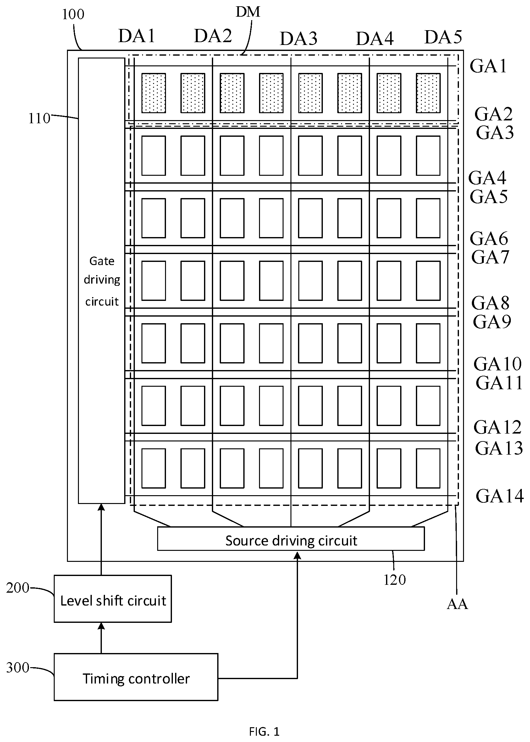
Referring to , the display apparatus may include a display panel 100 , a level shift circuit 200 and a timing controller 300 . Herein, the display panel 100 may include a plurality of pixel units arranged in an array, a plurality of gate lines (for example, GA 1 , GA 2 , GA 3 , . . . GA 13 , GA 14 ), a plurality of data lines (for example, DA 1 , DA 2 , DA 3 , DA 4 , DA 5 ), a gate driving circuit 110 and a source driving circuit 120 . The gate driving circuit 110 is respectively coupled to the gate lines GA 1 , GA 2 , GA 3 , . . . GA 13 , GA 14 , and the source driving circuit 120 is respectively coupled to the data lines DA 1 , DA 2 , DA 3 , DA 4 , DA 5 . Herein, the timing controller 300 inputs a control signal to the level shift circuit 200 , so that the level shift circuit 200 inputs a control signal to the gate driving circuit 110 , thereby driving the gate lines GA 1 , GA 2 , GA 3 , . . . GA 13 , GA 14 , to control the connected transistors to be turned on. The timing controller 300 inputs a signal to the source driving circuit 120 , to make the source driving circuit 120 input a voltage to the data lines, so that the voltage on the data lines is input to the sub-pixels through the turned-on transistors to charge the sub-pixels, to realize the display function.
Exemplarily, each pixel unit includes a plurality of sub-pixels of different colors. For example, a pixel unit may include a red sub-pixel, a green sub-pixel and a blue sub-pixel, so that, red, green and blue colors can be mixed to achieve color display. Alternatively, a pixel unit may also include a red sub-pixel, a green sub-pixel, a blue sub-pixel and a white sub-pixel, so that color mixing can be performed through red, green, blue and white to achieve color display. Of course, in practical applications, the luminous colors of the sub-pixels in the pixel unit can be designed and determined according to the practical application environment, which is not limited here. In the following, description will be made by taking a pixel unit including a red sub-pixel, a green sub-pixel and a blue sub-pixel as an example.
In an embodiment of the present disclosure, each sub-pixel may include a transistor and a pixel electrode. Herein, each sub-pixel row can correspond to two gate lines, so that the pixel array in the present disclosure can be arranged in a double-gate structure, so as to reduce half of the data lines (that is, there is a data line between two adjacent columns of some of pixels, and there is no data line between two adjacent columns of others of pixels). Exemplarily, a first sub-pixel row corresponds to gate lines GA 1 and GA 2 , a second sub-pixel row corresponds to gate lines GA 3 and GA 4 , a third sub-pixel row corresponds to gate lines GA 5 and GA 6 , a fourth sub-pixel row corresponds to gate lines GA 7 and GA 8 , a fifth sub-pixel row corresponds to gate lines GA 9 and GA 10 , a sixth sub-pixel row corresponds to gate lines GA 11 and GA 12 , and a seventh sub-pixel row corresponds to gate lines GA 13 and GA 14 .
In the embodiments of the present disclosure, a plurality of sub-pixels in the display panel can be divided into a plurality of sub-pixel groups, and each sub-pixel group can include two adjacent sub-pixels in the same row. In addition, one sub-pixel in the sub-pixel group is electrically connected to one of the corresponding two gate lines, and the other sub-pixel is electrically connected to the other of the corresponding two gate lines. Exemplarily, as shown in , in the first sub-pixel row, the red sub-pixel R 11 and the green sub-pixel G 11 are a sub-pixel group, the red sub-pixel R 11 is electrically connected to the gate line GA 1 , and the green sub-pixel G 11 is electrically connected to the gate line GA 2 . The blue sub-pixel B 11 and the red sub-pixel R 12 are a sub-pixel group, the blue sub-pixel B 11 is electrically connected to the gate line GA 1 , and the red sub-pixel R 12 is electrically connected to the gate line GA 2 . The green sub-pixel G 12 and the blue sub-pixel B 12 are a sub-pixel group, the green sub-pixel G 12 is electrically connected to the gate line GA 1 , and the blue sub-pixel B 12 is electrically connected to the gate line GA 2 . The red sub-pixel R 13 and the green sub-pixel G 13 are a sub-pixel group, the red sub-pixel R 13 is electrically connected to the gate line GA 1 , and the green sub-pixel G 13 is electrically connected to the gate line GA 2 . The blue sub-pixel B 13 and the red sub-pixel R 14 are a sub-pixel group, the blue sub-pixel B 13 is electrically connected to the gate line GA 1 , and the red sub-pixel R 14 is electrically connected to the gate line GA 2 . The green sub-pixel G 14 and the blue sub-pixel B 14 are a sub-pixel group, the green sub-pixel G 14 is electrically connected to the gate line GA 1 , and the blue sub-pixel B 14 is electrically connected to the gate line GA 2 . That is, a corresponding sub-pixel group in the nth row of sub-pixels is respectively connected to the (2n−1)th gate line and the (2n)th gate line, two sub-pixels included in a sub-pixel group are connected to the same data line, and two adjacent rows of sub-pixels corresponding to the same column of sub-pixel group are connected to two adjacent data lines, for example, R 11 and G 11 are connected to DA 1 , and R 21 and G 21 are connected to DA 2 .
Moreover, in the second sub-pixel row, the red sub-pixel R 21 and the green sub-pixel G 21 are a sub-pixel group, the red sub-pixel R 21 is electrically connected to the gate line GA 3 , and the green sub-pixel G 21 is electrically connected to the gate line GA 4 . The blue sub-pixel B 21 and the red sub-pixel R 22 are a sub-pixel group, the blue sub-pixel B 21 is electrically connected to the gate line GA 3 , and the red sub-pixel R 22 is electrically connected to the gate line GA 4 . The green sub-pixel G 22 and the blue sub-pixel B 22 are a sub-pixel group, the green sub-pixel G 22 is electrically connected to the gate line GA 3 , and the blue sub-pixel B 22 is electrically connected to the gate line GA 4 . The red sub-pixel R 23 and the green sub-pixel G 23 are a sub-pixel group, the red sub-pixel R 23 is electrically connected to the gate line GA 3 , and the green sub-pixel G 23 is electrically connected to the gate line GA 4 . The blue sub-pixel B 23 and the red sub-pixel R 24 are a sub-pixel group, the blue sub-pixel B 23 is electrically connected to the gate line GA 3 , and the red sub-pixel R 24 is electrically connected to the gate line GA 4 . The green sub-pixel G 24 and the blue sub-pixel B 24 are a sub-pixel group, the green sub-pixel G 24 is electrically connected to the gate line GA 3 , and the blue sub-pixel B 24 is electrically connected to the gate line GA 4 . The rest of the sub-pixel rows are similarly divided into sub-pixel groups, which will not be repeated here.
Exemplarily, as shown in , in the first sub-pixel row, the red sub-pixel R 11 and the green sub-pixel G 11 are a sub-pixel group, the red sub-pixel R 11 is electrically connected to the gate line GA 1 , and the green sub-pixel G 11 is electrically connected to the gate line GA 2 . The blue sub-pixel B 11 and the red sub-pixel R 12 are a sub-pixel group, the blue sub-pixel B 11 is electrically connected to the gate line GA 1 , and the red sub-pixel R 12 is electrically connected to the gate line GA 2 . The green sub-pixel G 12 and the blue sub-pixel B 12 are a sub-pixel group, the green sub-pixel G 12 is electrically connected to the gate line GA 1 , and the blue sub-pixel B 12 is electrically connected to the gate line GA 2 . The red sub-pixel R 13 and the green sub-pixel G 13 are a sub-pixel group, the red sub-pixel R 13 is electrically connected to the gate line GA 1 , and the green sub-pixel G 13 is electrically connected to the gate line GA 2 . The blue sub-pixel B 13 and the red sub-pixel R 14 are a sub-pixel group, the blue sub-pixel B 13 is electrically connected to the gate line GA 1 , and the red sub-pixel R 14 is electrically connected to the gate line GA 2 . The green sub-pixel G 14 and the blue sub-pixel B 14 are a sub-pixel group, the green sub-pixel G 14 is electrically connected to the gate line GA 1 , and the blue sub-pixel B 14 is electrically connected to the gate line GA 2 .
Moreover, in the second sub-pixel row, the red sub-pixel R 21 and the green sub-pixel G 21 are a sub-pixel group, the red sub-pixel R 21 is electrically connected to the gate line GA 3 , and the green sub-pixel G 21 is electrically connected to the gate line GA 4 . The blue sub-pixel B 21 and the red sub-pixel R 22 are a sub-pixel group, the blue sub-pixel B 21 is electrically connected to the gate line GA 3 , and the red sub-pixel R 22 is electrically connected to the gate line GA 4 . The green sub-pixel G 22 and the blue sub-pixel B 22 are a sub-pixel group, the green sub-pixel G 22 is electrically connected to the gate line GA 3 , and the blue sub-pixel B 22 is electrically connected to the gate line GA 4 . The red sub-pixel R 23 and the green sub-pixel G 23 are a sub-pixel group, the red sub-pixel R 23 is electrically connected to the gate line GA 3 , and the green sub-pixel G 23 is electrically connected to the gate line GA 4 . The blue sub-pixel B 23 and the red sub-pixel R 24 are a sub-pixel group, the blue sub-pixel B 23 is electrically connected to the gate line GA 3 , and the red sub-pixel R 24 is electrically connected to the gate line GA 4 . The green sub-pixel G 24 and the blue sub-pixel B 24 are a sub-pixel group, the green sub-pixel G 24 is electrically connected to the gate line GA 3 , and the blue sub-pixel B 24 is electrically connected to the gate line GA 4 . The rest of the sub-pixel rows are similarly divided into sub-pixel groups, which will not be repeated here.
In the embodiment of the present disclosure, a column of sub-pixel groups can be arranged between every two adjacent data lines; and for two adjacent data lines, one data line is connected to the odd-numbered rows of a column of sub-pixel groups between the two adjacent data lines, and the other data line is connected to the even-numbered rows of a column of sub-pixel groups arranged between the two adjacent data lines. In other words, two adjacent columns of sub-pixels are arranged between two adjacent data lines. This can reduce the power consumption of the source driving circuit. Exemplarily, as shown in and , the first column of sub-pixel groups LX 1 are arranged between the data lines DA 1 and DA 2 , the second column of sub-pixel groups LX 2 are arranged between the data lines DA 2 and DA 3 , the third column of sub-pixel groups LX 3 are arranged between the data lines DA 3 and DA 4 , the fourth column of sub-pixel groups LX 4 are arranged between the data lines DA 4 and DA 5 , the fifth column of sub-pixel groups LX 5 are arranged between the data lines DA 5 and DA 6 , and the sixth column of sub-pixel groups LX 6 are arranged between the data lines DA 6 and DA 7 .
For the first column of sub-pixel groups LX 1 : the data line DA 1 is electrically connected to the odd-numbered rows of the first column of sub-pixel groups LX 1 (that is, the red sub-pixel R 11 and the green sub-pixel G 11 in the first row; the red sub-pixel R 31 and the green sub-pixel G 31 in the third row; the red sub-pixel R 51 and the green sub-pixel G 51 in the fifth row; and the red sub-pixel R 71 and the green sub-pixel G 71 in the seventh row); and the data line DA 2 is electrically connected to the even-numbered rows of the first column of sub-pixel groups LX 1 (that is, the red sub-pixel R 21 and the green sub-pixel G 21 in the second row; the red sub-pixel R 41 and the green sub-pixel G 41 in the fourth row; and the red sub-pixel R 61 and the green sub-pixel G 61 in the sixth row).
For the second column of sub-pixel groups LX 2 : the data line DA 2 is electrically connected to the odd-numbered rows of the second column of sub-pixel groups LX 2 (that is, the blue sub-pixel B 11 and the red sub-pixel R 12 in the first row; the blue sub-pixel B 31 and the red sub-pixel R 32 in the third row; the blue sub-pixel B 51 and the red sub-pixel R 52 in the fifth row; and the blue sub-pixel B 71 and the red sub-pixel R 72 in the seventh row); and the data line DA 3 is electrically connected to the even-numbered rows of the second column of sub-pixel groups LX 2 (that is, the blue sub-pixel B 21 and the red sub-pixel R 22 in the second row; the blue sub-pixel B 41 and the red sub-pixel R 42 in the fourth row; and the blue sub-pixel B 61 and the red sub-pixel R 62 in the sixth row).
The rest of the sub-pixel groups are similarly connected to the data lines, which will not be repeated here.
Taking the structure of the display panel shown in as an example, is a timing diagram of some signals provided by an embodiment of the present disclosure. Herein, ga 1 represents the signal loaded on the gate line GA 1 , ga 2 represents the signal loaded on the gate line GA 2 , ga 3 represents the signal loaded on the gate line GA 3 , . . . ga 13 represents the signal loaded on the gate line GA 13 , and ga 14 represents the signal loaded on the gate line GA 14 . For example, the high level of the signals ga 1 -ga 14 can be used as a gate-on signal to control the transistors in the sub-pixels to be turned on. Referring to and , when controlling the drive of the display panel, the gate-on signals may be sequentially applied to the gate lines GA 1 -GA 14 . Taking the gate lines GA 1 -GA 6 , the data line DA 2 , and the sub-pixels connected to the data line DA 2 as an example, in the display frame F 1 , when the signal ga 1 on the first gate line GA 1 outputs a high-level gate-on signal, the transistor in the blue sub-pixel B 11 is turned on. In the time period T 11 corresponding to the high level of the signal ga 1 , the data voltage Vb 11 of the display data corresponding to the blue sub-pixel B 11 is input to the data line DA 2 , so that the blue sub-pixel B 11 is charged with the data voltage Vb 11 . In the time period T 11 , the signal ga 2 on the second gate line GA 2 outputs a high-level gate-on signal, and the transistor in the red sub-pixel R 12 is turned on. The data voltage Vb 11 is simultaneously input into the red sub-pixel R 12 to pre-charge the red sub-pixel R 12 , that is, Vb 11 is used as the pre-charge voltage of the red sub-pixel R 12 .
In the time period T 12 corresponding to the high level of the signal ga 2 , the data voltage Vr 12 of the display data corresponding to the red sub-pixel R 12 is input to the data line DA 2 , so that the red sub-pixel R 12 is charged with the data voltage Vr 12 . In the time period T 12 , the signal ga 3 on the third gate line GA 3 outputs a high-level gate-on signal, and the transistor in the red sub-pixel R 21 is turned on. The data voltage Vr 12 is simultaneously input into the red sub-pixel R 21 to pre-charge the red sub-pixel R 21 , that is, Vr 12 is used as the pre-charge voltage of the red sub-pixel R 21 .
In the time period T 13 corresponding to the high level of the signal ga 3 , the data voltage Vr 21 of the display data corresponding to the red sub-pixel R 21 is input to the data line DA 2 , so that the red sub-pixel R 21 is charged with the data voltage Vr 21 . In the time period T 13 , the signal ga 4 on the fourth gate line GA 4 outputs a high-level gate-on signal, and the transistor in the green sub-pixel G 21 is turned on. The data voltage Vr 21 is simultaneously input into the green sub-pixel G 21 to pre-charge the green sub-pixel G 21 , that is, Vr 21 serves as the pre-charge voltage of the green sub-pixel G 21 .
In the time period T 14 corresponding to the high level of the signal ga 4 , the data voltage Vg 21 of the display data corresponding to the green sub-pixel G 21 is input to the data line DA 2 , so that the green sub-pixel G 21 is charged with the data voltage Vg 21 . In the time period T 14 , the signal ga 5 on the fifth gate line GA 5 outputs a high-level gate-on signal, and the transistor in the blue sub-pixel B 31 is turned on. The data voltage Vg 21 is simultaneously input into the blue sub-pixel B 31 to pre-charge the blue sub-pixel B 31 , that is, Vg 21 is used as the pre-charge voltage of the blue sub-pixel B 31 .
In the time period T 15 corresponding to the high level of the signal ga 5 , the data voltage Vb 31 of the display data corresponding to the blue sub-pixel B 31 is input to the data line DA 2 , so that the blue sub-pixel B 31 is charged with the data voltage Vb 31 . In the time period T 15 , the signal ga 6 on the sixth gate line GA 6 outputs a high-level gate-on signal, and the transistor in the red sub-pixel R 32 is turned on. The data voltage Vb 31 is simultaneously input into the red sub-pixel R 32 to pre-charge the red sub-pixel R 32 , that is, Vb 31 is used as the pre-charge voltage of the red sub-pixel R 32 .
The implementation manners of the remaining sub-pixels are deduced in turn until the sub-pixels in the entire display panel are charged with the target voltage, which will not be repeated here.
During the driving process of the above-mentioned display panel, the voltage charged in the red sub-pixel R 12 jumps directly from Vb 11 to Vr 12 , and the voltage charged in the red sub-pixel R 21 jumps directly from Vr 12 to Vr 21 , for example, jumping directly from the voltage corresponding to the grayscale value of 127 to the voltage corresponding to the grayscale value of 255, resulting in different charging rates, thereby causing abnormal brightness, which in turn affects the display quality of the screen.
Based on this, an embodiment of the present disclosure provides a method for driving a display panel. When the gate-on signals loaded to adjacent M gate lines have an overlapping time, during the overlapping time, the sub-pixel electrically connected to the Mth gate line in the M gate lines is charged with the pre-charge voltage and the compensation voltage in sequence; and when the target voltage is charged to the sub-pixel electrically connected to the Mth gate line, the pre-charge voltage in the sub-pixel can be switched to the compensation voltage first, and then the compensation voltage is switched to the target voltage, so as to increase the charging rate, improve the brightness abnormality, and improve the picture display quality.
The method for driving the display panel provided by the embodiment of the present disclosure, as shown in , may include:
•
• S 10 . receiving display data of an image to be displayed in a current display frame; and • S 20 . controlling the display panel to apply a gate-on signal to gate lines in sequence, and input a voltage to data lines according to the display data.
In the embodiment of the present disclosure, when the gate-on signals loaded on adjacent M gate lines have an overlapping time, within the overlapping time, the sub-pixels electrically connected to the Mth gate line among the M gate lines are charged with the pre-charge voltage and the compensation voltage in sequence. After the overlapping time and during the time when the Mth gate line is loaded with the gate-on signal, the sub-pixels electrically connected to the Mth gate line are charged with the target voltage corresponding to the display data. Herein, the target voltage refers to the data voltage of the display data corresponding to the sub-pixel.
In the embodiment of the present disclosure, as shown in A , M=2, so that there is an overlapping time between the gate-on signals loaded on two adjacent gate lines, and in the overlapping time, the sub-pixels electrically connected to the second gate line among the two adjacent gate lines are charged with the pre-charge voltage, the compensation voltage and the target voltage in sequence. The image to be displayed can be displayed after each sub-pixel is charged with the target voltage. Exemplarily, taking the high level of the gate-on signal as an example, there is an overlapping time T 11 between the high level of the signal ga 1 of the first gate line GA 1 and the high level of the signal ga 2 of the second gate line GA 2 ; and then the second gate line GA 2 can be used as the second of two overlapping gate lines, and the first gate line GA 1 can be used as the first of two overlapping gate lines. There is an overlapping time T 12 between the high level of the signal ga 2 of the second gate line GA 2 and the high level of the signal ga 3 of the third gate line GA 3 ; and then the third gate line GA 3 can be used as the second of two overlapping gate lines, and the second gate line GA 2 is used as the first of two overlapping gate lines. There is an overlapping time T 13 between the high level of the signal ga 3 of the third gate line GA 3 and the high level of the signal ga 4 of the fourth gate line GA 4 ; and then the fourth gate line GA 4 can be used as the second of two gate lines, and the third gate line GA 3 is used as the first of two overlapping gate lines. There is an overlapping time T 14 between the high level of the signal ga 4 of the fourth gate line GA 4 and the high level of the signal ga 5 of the fifth gate line GA 5 , and then the fifth gate line GA 5 can be used as the second of two overlapping gate lines, and the fourth gate line GA 4 is used as the first of two overlapping gate lines. There is an overlapping time T 15 between the high level of the signal ga 5 of the fifth gate line GA 5 and the high level of the signal ga 6 of the sixth gate line GA 6 , and then the sixth gate line GA 6 can be used as the second of two overlapping gate lines, and the fifth gate line GA 5 is used as the first of two overlapping gate lines.
In the embodiment of the present disclosure, as shown in B , M=3, so that there is an overlapping time between the gate-on signals loaded on three adjacent gate lines, and during the overlapping time, the sub-pixels electrically connected to the third gate line among the three gate lines are charged with the pre-charge voltage, the compensation voltage and the target voltage in sequence. The image to be displayed can be displayed after each sub-pixel is charged with the target voltage. Exemplarily, taking the high level of the gate-on signal as an example, there is an overlapping time between the high level of the signal ga 1 of the first gate line GA 1 , the high level of the signal ga 2 of the second gate line GA 2 , and the high level of the signal ga 3 of the third gate line GA 3 ; and then the third gate line GA 3 can be used as the third of three overlapping gate lines. The rest are similar, and so on, which will not be repeated here.
In the embodiment of the present invention, as shown in C , M=4, so that there is an overlapping time between the gate-on signals loaded on four adjacent gate lines, and during the overlapping time, the sub-pixels electrically connected to the fourth gate line among the four gate lines are charged with the pre-charge voltage, the compensation voltage and the target voltage in sequence. The image to be displayed can be displayed after each sub-pixel is charged with the target voltage. Exemplarily, taking the high level of the gate-on signal as an example, there is an overlapping time between the high level of the signal ga 1 of the first gate line GA 1 , the high level of the signal ga 2 of the second gate line GA 2 , the high level of the signal ga 3 of the third gate line GA 3 and the high level of the signal ga 4 of the fourth gate line GA 4 , and then the fourth gate line GA 4 can be used as the fourth of the four overlapping gate lines. The rest are similar, and so on, which will not be repeated here.
Of course, M can be set to 5, 6 or greater, which can be designed and determined according to the requirements of practical applications, and is not limited here.
In order to improve the display quality of the picture, dummy sub-pixels can be set in the non-display area of the display panel. Exemplarily, in the embodiment of the present disclosure, as shown in to , the sub-pixels with shadows in the display panel can be used as dummy sub-pixels, and the rest of the sub-pixels can be used as display sub-pixels. The dummy sub-pixels are located on the peripheral area of the display sub-pixels. That is, the area where the display sub-pixels are located is the display area AA. The area on the substrate other than the display area AA can be a non-display area. The gate driving circuit 110 and the source driving circuit 120 can be arranged in the non-display area. The dummy sub-pixels may be in the dummy area DM of the non-display area. As shown in and , all sub-pixels in the first row may be used as dummy sub-pixels. That is, all sub-pixels in the first row are disposed in the dummy area DM. Alternatively, all sub-pixels in the first row and the second row may be used as dummy sub-pixels. That is, all sub-pixels in the first row and the second row are disposed in the dummy area DM. Certainly, in practical applications, the number of dummy sub-pixels may be set according to requirements of practical applications, which is not limited here.
In the following, taking M=2, the data line DA 2 and the first row of sub-pixels set as dummy sub-pixels for an example.
Combining and A , there is an overlapping time between the gate-on signal in the signal ga 1 of the first gate line GA 1 and the gate-on signal in the signal ga 2 of the second gate line GA 2 , and the overlapping time is the time period T 11 . The pre-charge voltage Vb 11 and the compensation voltage VBr 12 may be sequentially charged to the red sub-pixel R 12 during the time period T 11 . During the time period T 12 , the red sub-pixel R 12 is charged with the target voltage Vr 12 .
There is an overlapping time between the gate-on signal in the signal ga 2 of the second gate line GA 2 and the gate-on signal in the signal ga 3 of the third gate line GA 3 , and the overlapping time is the time period T 12 . During the time period T 12 , the red sub-pixel R 21 is charged with the pre-charge voltage Vr 12 and the compensation voltage VBr 21 in sequence. During the time period T 13 , the red sub-pixel R 21 is charged with the target voltage Vr 21 .
There is an overlapping time between the gate-on signal in the signal ga 3 of the third gate line GA 3 and the gate-on signal in the signal ga 4 of the fourth gate line GA 4 , and the overlapping time is the time period T 13 . During the time period T 13 , the green sub-pixel G 21 is charged with the pre-charge voltage Vr 21 and the compensation voltage VBg 21 in sequence. During the time period T 14 , the green sub-pixel G 21 is charged with the target voltage Vg 21 .
There is an overlapping time between the gate-on signal in the signal ga 4 of the fourth gate line GA 4 and the gate-on signal in the signal ga 5 of the fifth gate line GA 5 , and the overlapping time is the time period T 14 . During the time period T 14 , the blue sub-pixel B 31 is charged with the pre-charge voltage Vg 21 and the compensation voltage VBb 31 sequentially. During the time period T 15 , the blue sub-pixel B 31 is charged with the target voltage Vb 31 .
There is an overlapping time between the gate-on signal in the signal ga 5 of the fifth gate line GA 5 and the gate-on signal in the signal ga 6 of the sixth gate line GA 6 , and the overlapping time is the time period T 15 . During the time period T 15 , the red sub-pixel R 32 is charged with the pre-charge voltage Vb 31 and the compensation voltage VBr 32 in sequence. During the time period T 16 , the red sub-pixel R 32 is charged with the target voltage Vr 32 .
The implementation manners of the remaining sub-pixels are deduced in turn until the sub-pixels in the entire display panel are charged with the target voltage, which will not be repeated here.
In the embodiment of the present disclosure, as shown in , the V-By-One receiving end VBO-RX of the timing controller 300 can receive the display data of the image to be displayed in the current display frame, and input the display data in the form of binary digital voltage signal into the early warning module. The early warning module can judge whether the received display data is normal. If it is not normal, then the display data corresponding to the reminder picture (the reminder picture can be a red solid color picture or a green solid color picture or a blue solid color picture) is output to the brightness correction module. If it is normal, then the received display data is directly output to the brightness correction module. In this way, the input time of the compensation voltage and the compensation voltage can be determined by the brightness correction module in the timing controller 300 according to the received display data. In this way, the driving module in the timing controller 300 outputs control signals to the gate driving circuit 110 and the source driving circuit 120 in the display panel according to the display data output by the brightness correction module and the determined input time of the compensation voltage and compensation voltage, to control the display panel to sequentially apply a gate-on signal to the gate lines, convert the display data from a digital voltage signal to an analog voltage signal, and then input a voltage to the data lines. Therefore, when the gate-on signals loaded on adjacent M gate lines have an overlapping time, during the overlapping time, the sub-pixels electrically connected to the Mth gate line among the M gate lines are sequentially charged with the pre-charge voltage and the compensation voltage. After the overlapping time and during the time when the Mth gate line is loaded with the gate-on signal, the sub-pixels electrically connected to the Mth gate line are charged with the target voltage corresponding to the display data.
In some examples, the display data of the image to be displayed may include: display data corresponding to each sub-pixel in a one-to-one manner. The grayscale value of the target voltage corresponding to the dummy sub-pixel adjacent to the display sub-pixel can be the same as the grayscale value of the target voltage corresponding to the display sub-pixel. In this way, the grayscale value of the dummy sub-pixel adjacent to the display sub-pixel can follow the display sub-pixel, that is, the grayscale value of the display sub-pixel is the same as the grayscale value of dummy sub-pixel adjacent to the display sub-pixel. For example, taking the first row of sub-pixels as dummy sub-pixels and the second row of sub-pixels as display sub-pixels, the grayscale value of the target voltage of the red sub-pixel R 11 is the same as the grayscale value of the target voltage of the red sub-pixel R 21 , the grayscale value of the target voltage of the green sub-pixel G 11 is the same as the grayscale value of the target voltage of the green sub-pixel G 21 , and the grayscale value of the target voltage of the blue sub-pixel B 11 is the same as the grayscale value of the target voltage of the blue sub-pixel B 21 . The grayscale value of the target voltage of the red sub-pixel R 12 is the same as the grayscale value of the target voltage of the red sub-pixel R 22 , the grayscale value of the target voltage of the green sub-pixel G 12 is the same as the grayscale value of the target voltage of the green sub-pixel G 22 , and the grayscale value of the target voltage of the blue sub-pixel B 12 is the same as the grayscale value of the target voltage of the blue sub-pixel B 22 . The grayscale value of the target voltage of the red sub-pixel R 13 is the same as the grayscale value of the target voltage of the red sub-pixel R 23 , the grayscale value of the target voltage of the green sub-pixel G 13 is the same as the grayscale value of the target voltage of the green sub-pixel G 23 , and the grayscale value of the target voltage of the blue sub-pixel B 13 is the same as the grayscale value of the target voltage of the blue sub-pixel B 23 . The grayscale value of the target voltage of the red sub-pixel R 14 is the same as the grayscale value of the target voltage of the red sub-pixel R 24 , the grayscale value of the target voltage of the green sub-pixel G 14 is the same as the grayscale value of the target voltage of the green sub-pixel G 24 , and the grayscale value of the target voltage of the blue sub-pixel B 14 is the same as the grayscale value of the target voltage of the blue sub-pixel B 24 .
In some examples, if the sub-pixels in the first row and the second row are dummy sub-pixels, and the sub-pixels in the third row are display sub-pixels, in the same column of sub-pixels, the grayscale value of the target voltage corresponding to the sub-pixels in the second row can be the same as the grayscale value of the target voltage corresponding to the sub-pixels in the third row. The grayscale value of each sub-pixel in the first row can be set as a fixed grayscale value.
In some examples, when the grayscale value of the display data corresponding to each sub-pixel is the same grayscale value, the pre-charge voltage, the compensation voltage and the target voltage can be the same. In this way, the difficulty of determining the compensation voltage can be reduced, and the amount of calculation can be reduced.
Taking the display panel with grayscale values from 0 to 255 as an example, for example, the sub-pixels in the first row are dummy sub-pixels. In the related art, the grayscale value of the display data corresponding to the dummy sub-pixels is usually set to a fixed value, such as a fixed grayscale value 127. When the picture to be displayed is the picture with the same grayscale value (that is, a pure grayscale picture), displaying a picture of grayscale value 64 is taken as an example. In this case, taking the sub-pixel connected to the third grate line being the red sub-pixel R 21 as an example, the pre-charge voltage of the red sub-pixel R 21 is the voltage corresponding to the grayscale value 127, and then the red sub-pixel R 21 is charged with the target voltage of the grayscale value 64. In the sub-pixels from the third row to the seventh row, the pre-charge voltage of the red sub-pixels is the voltage corresponding to grayscale value 64, and then the red sub-pixels are charged with the target voltage of grayscale value 64, that is, the voltage of the first row of sub-pixel jumps from the pre-charge voltage of grayscale value 127 to the target voltage of grayscale value 64, while the other rows of sub-pixels still change from the pre-charge voltage of grayscale value 64 to the target voltage of grayscale value 64. As a result, the brightness of the sub-pixels in the second row is higher, and there is a difference between the brightness of the second row and the brightness of other display rows, resulting in the problem of uneven display. In the embodiment of the present disclosure, by setting the grayscale value of the corresponding display data of each sub-pixel to the same grayscale value, the display data of the sub-pixels in the first row can be the same as the display data of the sub-pixels in the second row. Taking the red sub-pixel R 21 as an example, the pre-charge voltage, the compensation voltage and the target voltage charged to the red sub-pixel R 21 are voltages corresponding to the grayscale value 64. In the sub-pixels of the third row to the seventh row, the pre-charge voltage, the compensation voltage and the target voltage charged to the red sub-pixels are also voltages corresponding to the grayscale value 64. In this way, the uniformity of the charging rate of the sub-pixels in the second row to the seventh row can be improved, and the uniformity of brightness can also be improved. Since the sub-pixels in the first row are dummy sub-pixels, which do not need to display an image, and the brightness uniformity of the sub-pixels in the second to seventh rows for display is improved, thus the image can be displayed normally. That is, in the embodiment of the present disclosure, by setting the target voltage corresponding to the grayscale value of the dummy sub-pixel row to be the same as the target voltage corresponding to the grayscale value of the adjacent display sub-pixel row, the pre-charge voltage, the compensation voltage and the target voltage of the display sub-pixel row are all equal, to realize the uniform display effect of the pure grayscale image; herein the specific target voltage corresponding to the equal grayscale value can be set according to the display sub-pixel row.
Of course, in order to reduce the calculation amount and power consumption of the timing controller, the compensation voltage may be first input to the sub-pixels connected to the first gate line, and then the target voltage may be input.
Exemplarily, taking the display panel with grayscale values from 0 to 255 as an example, when the grayscale value of the display data corresponding to each sub-pixel is grayscale value 64, the image to be displayed can be a frame with a pure grayscale value. Combined with and A , before the time period T 11 , the blue sub-pixel B 11 can be charged with the compensation voltage VBb 11 . During the time period T 11 , the target voltage Vb 11 charged to the blue sub-pixel B 11 is the voltage corresponding to grayscale value 64. The pre-charge voltage Vb 11 and the compensation voltage VBr 12 charged to the red sub-pixel R 12 in sequence during the time period T 11 , and the target voltage Vr 12 charged to the red sub-pixel R 12 during the time period T 12 are a voltage corresponding to the grayscale value 64. The pre-charge voltage Vr 12 and the compensation voltage VBr 21 charged to the red sub-pixel R 21 sequentially during the time period T 12 , and the target voltage Vr 21 charged to the red sub-pixel R 21 during the time period T 13 are a voltage corresponding to the grayscale value 64. The pre-charge voltage Vr 21 and the compensation voltage VBg 21 charged to the green sub-pixel G 21 sequentially during the time period T 13 , and the target voltage Vg 21 charged to the green sub-pixel G 21 during the time period T 14 are a voltage corresponding to the grayscale value 64. The pre-charge voltage Vg 21 and the compensation voltage VBb 31 charged to the blue sub-pixel B 31 sequentially during the time period T 14 , and the target voltage Vb 31 charged to the blue sub-pixel B 31 during the time period T 15 are a voltage corresponding to the grayscale value 64. The pre-charge voltage Vb 31 and the compensation voltage VBr 32 charged to the red sub-pixel R 32 sequentially during the time period T 15 , and the target voltage Vr 32 charged to the red sub-pixel R 32 during the time period T 16 are a voltage corresponding to the grayscale value 64.
Of course, the grayscale value of the display data corresponding to each sub-pixel may also be the grayscale value 127, the grayscale value 255, etc., which can be determined according to the requirements of practical applications, and are not limited here.
In the embodiment of the present disclosure, as shown in A , the set edge of the compensation trigger signal TP 1 may be a falling edge, and the compensation voltage is triggered by the falling edge of the compensation trigger signal TP 1 and input to the data line connected to the corresponding sub-pixel. The falling edge of the compensation trigger signal is within the overlapping time. Exemplarily, a compensation voltage can be applied to the data line corresponding to the sub-pixel connected to the first gate line GA 1 under a trigger of a first falling edge of the compensation trigger signal TP 1 , so that the compensation voltage can be input to the sub-pixel connected to the first gate line GA 1 . The compensation voltage can be applied to the data line corresponding to the sub-pixel connected to the second gate line GA 2 under a trigger of a second falling edge of the compensation trigger signal TP 1 , so that the compensation voltage can be input to the sub-pixel connected to the second gate line GA 2 . The compensation voltage can be applied to the data line corresponding to the sub-pixel connected to the third gate line GA 3 under a trigger of a third falling edge of the compensation trigger signal TP 1 , so that the compensation voltage can be input to the sub-pixel connected to the third gate line GA 3 . The compensation voltage can be applied to the data line corresponding to the sub-pixel connected to the fourth gate line GA 4 under a trigger of a fourth falling edge of the compensation trigger signal TP 1 , so that the compensation voltage can be input to the sub-pixel connected to the fourth gate line GA 4 . The compensation voltage can be applied to the data line corresponding to the sub-pixel connected to the fifth gate line GA 5 under a trigger of a fifth falling edge of the compensation trigger signal TP 1 , so that the compensation voltage can be input to the sub-pixel connected to the fifth gate line GA 5 . The rest are similar, and so on, which will not be repeated here.
In the embodiment of the present disclosure, as shown in A , A represents the maintenance duration of the overlapping time. When the set edge of the compensation trigger signal TP 1 is set as a falling edge, there is a first interval duration t 1 between the falling edge and a starting moment of the overlapping time, and the first interval duration t 1 may not be less than 1/2 A. If the falling edge of the compensation trigger signal TP 1 is at an earlier position of the overlapping time, the target voltage on the data line may need to be changed to the compensation voltage quickly, which may easily increase power consumption. In the embodiment of the present disclosure, by setting t 1 =1/2 A, the target voltage on the data line can be loaded for a certain period of time, and then switched to the compensation voltage to avoid excessive power consumption. Exemplarily, t 1 =1/2 A, or t 1 =2/3 A, or t 1 =3/4 A. Of course, in practical applications, the specific duration of t 1 can be determined according to requirements of practical applications, and is not limited here.
In the embodiment of the present disclosure, as shown in A , when the set edge of the compensation trigger signal TP 1 is set as a falling edge, there may be a second interval duration t 2 between the falling edge and an ending moment of the overlapping time. The second interval duration t 2 is not greater than 1/2 A. Since the falling edge is within the overlapping time, t 2 >0. By setting t 2 ≤1/2 A, the target voltage on the data line can be loaded for a certain period of time before switching to the compensation voltage to avoid excessive power consumption. Exemplarily, t 2 =1/2 A, or t 2 =1/3 A, or t 2 =1/4 A. Of course, in practical applications, the specific duration of t 2 may be determined according to requirements of practical applications, and is not limited here.
It should be noted that the set edge of the compensation trigger signal TP 1 can also be set as a rising edge, and the method of loading the compensation voltage triggered by the rising edge can refer to the above-mentioned method of loading the compensation voltage triggered by the falling edge, which will not be repeated here.
In the embodiment of the present disclosure, as shown in A , the set edge of the target trigger signal TP 2 can be set as a falling edge, and the target voltage is triggered by the falling edge of the target trigger signal TP 2 and input to the data line connected to the corresponding sub-pixel. Exemplarily, a target voltage can be applied to the data line corresponding to the sub-pixel connected to the first gate line GA 1 under a trigger of the first falling edge of the target trigger signal TP 2 , so that the target voltage can be input to the sub-pixel connected to the first gate line GA 1 . The target voltage can be applied to the data line corresponding to the sub-pixel connected to the second gate line GA 2 under a trigger of the second falling edge of the target trigger signal TP 2 , so that the target voltage can be input to the sub-pixel connected to the second gate line GA 2 . The target voltage can be applied to the data line corresponding to the sub-pixel connected to the third gate line GA 3 under a trigger of the third falling edge of the target trigger signal TP 2 , so that the target voltage can be input to the sub-pixel connected to the third gate line GA 3 . The target voltage can be applied to the data line corresponding to the sub-pixel connected to the fourth gate line GA 4 under a trigger of the fourth falling edge of the target trigger signal TP 2 , so that the target voltage can be input to the sub-pixel connected to the fourth gate line GA 4 . The target voltage can be applied to the data line corresponding to the sub-pixel connected to the fifth gate line GA 5 under a trigger of the fifth falling edge of the target trigger signal TP 2 , so that the target voltage can be input to the sub-pixel connected to the fifth gate line GA 5 . The rest are similar, and so on, which will not be repeated here.
In the embodiment of the present disclosure, as shown in A , the falling edge of the target trigger signal TP 2 can be after the ending moment of the overlapping time, so as to avoid the subsequent charging of the target voltage from causing influence to the sub-pixels already charged with the target voltage. Of course, the falling edge of the target trigger signal TP 2 may also be aligned with the ending moment of the overlapping time. In this way, the influence of the target voltage charged later on the sub-pixels already charged with the target voltage can be avoided, and the sub-pixels can be charged with the target voltage in the maximum time, further improving the charging rate.
It should be noted that due to the delay of the signal, it may take a certain delay time when the gate-on signal is switched from a high level to a low level. After the delay time, the transition from the high level to the low level may be completed. If the set edge of the target trigger signal is within the delay time, it also belongs to the protection scope of the alignment mentioned in the present disclosure.
It should be noted that the set edge of the target trigger signal TP 2 can also be set as a rising edge, and the way of loading the target voltage triggered by the rising edge can refer to the above-mentioned way of loading the target voltage triggered by the falling edge, which will not be repeated here.
In the embodiment of the present disclosure, the target trigger signal TP 2 and the compensation trigger signal TP 1 can be set as independent signals, so that the moment when the target voltage is input to the data line and the moment when the compensation voltage is input to the data line can be independently controlled.
Embodiments of the present invention provide other methods for driving display panels, which are modified for the implementation manners in the above-mentioned embodiments. The following only describes the differences between this embodiment and the above-mentioned embodiments, and the similarities will not be repeated here.
In the embodiment of the present disclosure, when the grayscale values of the display data corresponding to at least two sub-pixels are different grayscale values, the pre-charge voltage and the compensation voltage may be different. In this way, the compensation voltage can be set according to the actual target voltage, so that the compensation voltage can be flexibly controlled, and the effect of pre-charging can be further improved.
In an embodiment of the present disclosure, for the same sub-pixel, the relationship between the pre-charge voltage VY1, the compensation voltage VB1 and the target voltage VM1 which are charged to the sub-pixel may be: VM1<VB1<VY1. Since VY1>VM1, the sub-pixel will be brighter. That is, if the pre-charge voltage VY1 charged to the sub-pixel is greater than the target voltage VM1 corresponding to the sub-pixel, then the compensation voltage VB1 corresponding to the sub-pixel can satisfy: VM1<VB1<VY1. In the embodiment of the present disclosure, the compensation voltage VB1 can be set as an intermediate value between the pre-charge voltage VY1 and the target voltage VM1 by first switching the sub-pixel from the pre-charge voltage VY1 to the compensation voltage VB1, and then switching from the compensation voltage VB1 to the target voltage VM1, thereby increasing the charging rate, improving the abnormal brightness, and improving the picture display quality. In this way, the compensation voltage can be dynamically adjusted in real time according to the pre-charge voltage and target voltage corresponding to the sub-pixel, so that the compensation voltage of the display sub-pixels in the first row can be different from the compensation voltages of the display sub-pixels in other rows. The compensation voltages of the display sub-pixels all can also be set differently, thereby achieving precise compensation, further improving brightness uniformity, and improving display effects.
Of course, the compensation voltage VB1 can also follow the target voltage VM1 of the sub-pixel, which is equivalent to increasing the charging time of the target voltage, thereby increasing the charging rate.
In the embodiment of the present disclosure, for the same sub-pixel, the relationship between the pre-charge voltage VY2, the compensation voltage VB2 and the target voltage VM2 which are charged to the sub-pixel is: VY2<VB2<VM2. Since VY2<VM2, the sub-pixel will be darker. That is, if the pre-charge voltage VY2 charged to the sub-pixel is smaller than the target voltage VM2 corresponding to the sub-pixel, then the compensation voltage VB2 corresponding to the sub-pixel can satisfy: VY2<VB2<VM2. In the embodiment of the present disclosure, the compensation voltage VB2 can be set as an intermediate value between the pre-charge voltage VY2 and the target voltage VM2 by first switching the sub-pixel from the pre-charge voltage VY2 to the compensation voltage VB2, and then switching from the compensation voltage VB2 to the target voltage VM2, thereby increasing the charging rate, improving the abnormal brightness, and improving the picture display quality. In this way, the compensation voltage can be dynamically adjusted in real time according to the pre-charge voltage and target voltage corresponding to the sub-pixel, so that the compensation voltage of the display sub-pixels in the first row can be different from the compensation voltages of the display sub-pixels in other rows. The compensation voltages of the display sub-pixels all can also be set differently, thereby achieving precise compensation, further improving brightness uniformity, and improving display effects.
Of course, the compensation voltage VB2 can also follow the target voltage VM2 of the sub-pixel, which is equivalent to increasing the charging time of the target voltage, thereby increasing the charging rate.
Of course, the grayscale value of the compensation voltage corresponding to each display sub-pixel may also be the same. For example, when displaying a red solid-color picture with the grayscale value 64, the grayscale value of the compensation voltage of each display sub-pixel can be set to a grayscale value between grayscale values 0 and 64, for example, the grayscale value of the compensation voltage of each display sub-pixel is the grayscale value 40. In this way, it can also improve the display uniformity to a certain extent, and can reduce power consumption, and it is not necessary to reduce the amount of calculation and power consumption of the timing controller every time according to the difference between grayscale values of the pre-charge voltage and the target voltage.
It should be noted that when displaying a color image, the grayscale values of the target voltages corresponding to different display sub-pixels may be partly different, partly the same, or all different. For this, the compensation voltage can be dynamically adjust in real time according to the pre-charge voltage and target voltage corresponding to each display sub-pixel, so that the compensation voltage of the display sub-pixel can be accurately adjusted according to the specific charged pre-charge voltage and target voltage, further improving the brightness uniformity and improving the display effect.
In an embodiment of the present disclosure, according to the display data, controlling the display panel to sequentially apply a gate-on signal to the gate lines and input a voltage to the data lines, may specifically include: for sub-pixels electrically connected to the same data line, there is a grayscale value difference between the grayscale value of the display data corresponding to the sub-pixel connected to the Mth gate line and the grayscale value of the display data corresponding to the sub-pixel connected to the (M−1) th gate line; determining whether the grayscale value difference is not less than a grayscale value difference threshold. When it is determined that the grayscale value difference is not less than the grayscale value difference threshold, it can indicate that the brightness change (brightening or darkening) of the sub-pixel is more obvious, and it is easy to be noticed by human eyes. Therefore, during the overlapping time, after the sub-pixel electrically connected to the Mth gate line among the M gate lines is charged with the pre-charge voltage, a compensation voltage is input to the electrically connected data line. When it is determined that the grayscale value difference is less than the grayscale value difference threshold, it can indicate that the brightness change (brightening or darkening) of the sub-pixel is not too obvious, and it is not easy to be noticed by human eyes; and the abnormality of the displayed image can be negligible, so the target voltage can be directly input to the electrically connected data line.
In the embodiment of the present disclosure, the grayscale value difference threshold can be a grayscale value of 25, a grayscale value of 50, a grayscale value of 100, a grayscale value of 160, a grayscale value of 200, etc., which can be determined according to the actual application requirements, and is not limited here.
Of course, in the embodiment of the present disclosure, the above process of determining the grayscale value difference and determining the relationship between the grayscale value difference and the grayscale value difference threshold may not be additionally implemented. It is also possible to directly input the compensation voltage to the data line. This can reduce the amount of computation and reduce power consumption.
Exemplarily, taking the display panel with grayscale values of 0 to 255 as an example, if each red sub-pixel corresponds to display data with a grayscale value of 64, and the remaining sub-pixels correspond to display data with a grayscale value of 0, the display panel can display a red solid color screen. If each green sub-pixel corresponds to display data with a grayscale value of 64, and the remaining sub-pixels correspond to display data with a grayscale value of 0, the display panel can display a green solid color screen. If each blue sub-pixel corresponds to display data with a grayscale value of 64, and the remaining sub-pixels correspond to display data with a grayscale value of 0, the display panel can display a blue solid color screen.
Exemplarily, a display of a red solid color screen, each red sub-pixel corresponding to display data with a grayscale value of 64, and the remaining sub-pixels corresponding to display data with a grayscale value of 0 are taken as an example. Combining and , before the time period T 11 , the blue sub-pixel B 11 can be charged with the compensation voltage VBb 11 with a grayscale value of 0, and during the time period T 11 , the blue sub-pixel B 11 is charged with the target voltage L 0 with a grayscale value of 0. During the time period T 11 , the red sub-pixel R 12 is sequentially charged with the pre-charge voltage L 0 and the compensation voltage VBr 12 with a grayscale value of 40, and during the time period T 12 , the red sub-pixel R 12 is charged with the target voltage Vr 12 with a grayscale value of 64. During the time period T 12 , the red sub-pixel R 21 is sequentially charged with the pre-charge voltage Vr 12 and the compensation voltage VBr 21 with a grayscale value of 40, and during the time period T 13 , the red sub-pixel R 21 is charged with the target voltage Vr 21 with a grayscale value of 64. During the time period T 13 , the green sub-pixel G 21 is charged with the pre-charge voltage Vr 21 and the compensation voltage VBg 21 with a grayscale value of 40 in sequence, and during the time period T 14 , the green sub-pixel G 21 is charged with the target voltage L 0 with a grayscale value of 0. During the time period T 14 , the blue sub-pixel B 31 is charged with the pre-charge voltage L 0 and the compensation voltage VBb 31 with a grayscale value of 0 in sequence, and during the time period of T 15 , the blue sub-pixel B 31 is charged with the target voltage L 0 with a grayscale value of 0. During the time period T 15 , the red sub-pixel R 32 is sequentially charged with the pre-charge voltage L 0 and the compensation voltage VBr 32 with a grayscale value of 40, and during the time period T 16 , the red sub-pixel R 32 is charged with the target voltage with a grayscale value of 64.
It should be noted that the process of displaying the green solid color screen and the blue solid color screen may be basically the same as the above-mentioned process of displaying the red solid color screen, which will not be repeated here.
The embodiment of the present disclosure provides some other methods for driving the display panel, as shown in , which is modified for the implementation manner in the above-mentioned embodiments. The following only describes the differences between this embodiment and the above-mentioned embodiments, and the similarities will not be repeated here.
In the embodiment of the present disclosure, when the compensation voltage is set as the target voltage, the set edge of the compensation trigger signal may be set as the set edge of the target trigger signal that triggers the target voltage. In this way, there is no need to additionally set the target trigger signal, and the target voltage can be directly input to the data line under a trigger of the falling edge of the compensation trigger signal. In this way, after the data line is loaded with the previous target voltage, the next target voltage can be loaded directly according to the trigger of the falling edge of the compensation trigger signal, reducing voltage switching and further reducing power consumption.
Exemplarily, as shown in , the target voltage is triggered by the falling edge of the compensation trigger signal TP 1 and input to the data line connected to the corresponding sub-pixel, so as to be input into the sub-pixel as the compensation voltage and the target voltage. Exemplarily, a target voltage can be applied to the data line corresponding to the sub-pixel connected to the first gate line GA 1 under a trigger of the first falling edge of the compensation trigger signal TP 1 , so that the target voltage can be input to the sub-pixel connected to the first gate line GA 1 and can be used as the compensation voltage and the target voltage. The target voltage can be applied to the data line corresponding to the sub-pixel connected to the second gate line GA 2 under a trigger of the second falling edge of the compensation trigger signal TP 1 , so that the target voltage can be input to the sub-pixel connected to the second gate line GA 2 and can be used as the compensation voltage and the target voltage. The target voltage can be applied to the data line corresponding to the sub-pixel connected to the third gate line GA 3 under a trigger of the third falling edge of the compensation trigger signal TP 1 , so that the target voltage can be input to the sub-pixel connected to the third gate line GA 3 and can be used as the compensation voltage and the target voltage. The target voltage can be applied to the data line corresponding to the sub-pixel connected to the fourth gate line GA 4 under a trigger of the fourth falling edge of the compensation trigger signal TP 1 , so that the target voltage can be input to the sub-pixel connected to the fourth gate line GA 4 and can be used as the compensation voltage and the target voltage. The target voltage can be applied to the data line corresponding to the sub-pixel connected to the fifth gate line GA 5 under a trigger of the fifth falling edge of the compensation trigger signal TP 1 , so that the target voltage can be input to the sub-pixel connected to the fifth gate line GA 5 , and can be used as the compensation voltage and the target voltage. The rest are similar, and so on, which will not be repeated here.
It should be noted that, taking the set edge as the falling edge for an example, the falling edge of the compensation trigger signal TP 1 in this embodiment can be equivalent to moving forward the falling edge of the TP signal that triggers the data voltage by a certain time in the related art, so that it is not necessary to additionally set redundant trigger signals, and it is only necessary to move forward the falling edge of the TP signal that has already been matured in the process, so as to reduce the cost of hardware and/or too much modification.
In the embodiment of the present disclosure, the grayscale value of the target voltage corresponding to the dummy sub-pixel adjacent to the display sub-pixel can be the same as the grayscale value of the target voltage corresponding to the display sub-pixel, and the compensation voltage and the target voltage of the display sub-pixel adjacent to the dummy sub-pixel are the same. For example, as shown in , taking the first row of sub-pixels as dummy sub-pixels for an example, the grayscale value of the target voltage corresponding to the red sub-pixel R 11 is the same as the grayscale value of the target voltage corresponding to the red sub-pixel R 21 , and the compensation voltage corresponding to the red sub-pixel R 21 is the same as the target voltage. The grayscale value of the target voltage corresponding to the green sub-pixel G 11 is the same as the grayscale value of the target voltage corresponding to the green sub-pixel G 21 , and the compensation voltage corresponding to the green sub-pixel G 11 is the same as the target voltage. The grayscale value of the target voltage corresponding to the blue sub-pixel B 11 is the same as the grayscale value of the target voltage corresponding to the blue sub-pixel B 21 , and the compensation voltage corresponding to the blue sub-pixel B 11 is the same as the target voltage.
Exemplarily, a display of a red solid color screen and each red sub-pixel corresponding to the display data of 255 grayscale values are taken as an example, referring to and , before the time period T 11 , the blue sub-pixel B 11 can be charged with the compensation voltage VBb 11 with a grayscale value of 0, and during the time period T 11 , the blue sub-pixel B 11 is charged with the target voltage L 0 with a grayscale value of 0. During the time period T 11 , the red sub-pixel R 12 is charged with the pre-charge voltage L 0 and the compensation voltage VBr 12 with a grayscale value of 127 in sequence, and during the time period T 12 , the red sub-pixel R 12 is charged with the target voltage Vr 12 with a grayscale value of 255. During the time period T 12 , the red sub-pixel R 21 is charged with the pre-charge voltage Vr 12 and the compensation voltage VBr 21 with a grayscale value of 255 in sequence, and during the time period T 13 , the red sub-pixel R 21 is charged with the target voltage Vr 21 with a grayscale value of 255. During the time period T 13 , the green sub-pixel G 21 is charged with the pre-charge voltage Vr 21 and the compensation voltage VBg 21 with a grayscale value of 127 in sequence, and during the time period T 14 , the green sub-pixel G 21 is charged with the target voltage L 0 with a grayscale value of 0. During the time period T 14 , the blue sub-pixel B 31 is charged with the pre-charge voltage L 0 and the compensation voltage VBb 31 with a grayscale value of 0 in sequence, and during the time period T 15 , the blue sub-pixel B 31 is charged with the target voltage L 0 with a grayscale value of 0. During the time period T 15 , the red sub-pixel R 32 is charged with the pre-charge voltage L 0 and the compensation voltage VBr 32 with a grayscale value of 127 in sequence, and during the time period T 16 , the red sub-pixel R 32 is charged with the target voltage with a grayscale value of 255.
The following takes the green sub-pixel G 21 as an example to carry out a simulation. A is a schematic diagram of a simulation by using a driving method in the related art. B is a schematic diagram of a simulation by using a driving method in the embodiment of the present disclosure. Here, ga 4 represents the signal on the fourth gate line GA 4 , and G 21 -Vda represents the voltage input to the green sub-pixel G 21 . As shown in A , the green sub-pixel G 21 is first charged with a voltage L 255 corresponding to a grayscale value of 255 as a pre-charge voltage, and then charged with a voltage L 0 corresponding to a grayscale value of 0 as a target voltage. As shown in B , the green sub-pixel G 21 is first charged with the voltage L 255 corresponding to the grayscale value of 255 as the pre-charge voltage, then charged with the voltage L 127 corresponding to the grayscale value of 127 as the compensation voltage, and then charged with the voltage L 0 corresponding to the grayscale value of 0 as the target voltage. In this way, the charging rate can be improved, the abnormal brightness can be improved, and the picture display quality can be improved.
Those skilled in the art should understand that the embodiments of the present disclosure may be provided as methods, systems, or computer program products. Accordingly, the present disclosure can take the form of an entirely hardware embodiment, an entirely software embodiment, or an embodiment combining software and hardware aspects. Furthermore, the present disclosure may take the form of a computer program product embodied on one or more computer-usable storage media (including but not limited to the disk storage, compact disc read-only memory (CD-ROM), optical storage, etc.) having computer-usable program code embodied therein.
The present disclosure is described with reference to flowchart illustrations and/or block diagrams of methods, apparatus (systems), and computer program products according to embodiments of the disclosure. It should be understood that each procedure and/or block in the flowchart and/or block diagram, and a combination of procedures and/or blocks in the flowchart and/or block diagram can be realized by computer program instructions. These computer program instructions may be provided to a general purpose computer, a special purpose computer, an embedded processor, or a processor of other programmable data processing equipment to produce a machine, such that the instructions executed by the processor of the computer or other programmable data processing equipment produce an apparatus for realizing the functions specified in one or more procedures of the flowchart and/or one or more blocks of the block diagram.
These computer program instructions may also be stored in a computer-readable memory capable of directing a computer or other programmable data processing equipment to operate in a specific manner, such that the instructions stored in the computer-readable memory produce an article of manufacture including instruction devices, and the instruction device realizes the function specified in one or more procedures of the flowchart and/or one or more blocks of the block diagram.
These computer program instructions can also be loaded onto a computer or other programmable data processing equipment, causing a series of operational steps to be performed on the computer or other programmable equipment to produce a computer-implemented process, so that the instructions performed on the computer or other programmable equipment provide steps for implementing the functions specified in one or more procedures of the flowchart and/or one or more blocks of the block diagram.
While preferred embodiments of the disclosure have been described, additional changes and modifications to these embodiments can be made by those skilled in the art once the basic inventive concept is appreciated. Therefore, it is intended that the appended claims be construed to cover the preferred embodiment as well as all changes and modifications which fall within the scope of the disclosure.
Apparently, those skilled in the art can make various modifications and variations to the embodiments of the present disclosure without departing from the spirit and scope of the embodiments of the present disclosure. In this way, if the modifications and variations of the embodiments of the present disclosure fall within the scope of the claims of the present disclosure and their equivalent technologies, the present disclosure also intends to include these modifications and variations.
Figures (11)
Citations
This patent cites (39)
- US8786536
- US9299318
- US10522100
- US10665148
- US11087685
- US2004/0246224
- US2005/0110726
- US2005/0168491
- US2006/0192745
- US2006/0221015
- US2007/0046609
- US2008/0001893
- US2010/0207928
- US2011/0242140
- US2013/0169619
- US2014/0320521
- US2014/0368415
- US2015/0035866
- US2016/0049123
- US2016/0180817
- US2018/0182299
- US2018/0182325
- US2018/0196301
- US2018/0350306
- US2021/0183317
- US2021/0209987
- US2022/0406252
- US2023/0335056
- US2024/0046838
- US1924649
- US101135825
- US104347045
- US107065366
- US108305590
- US108735138
- US112017575
- US112394578
- US112540487
- US20110078375