Abstract
Provided is a display device comprising a display panel, an input sensor including a first sensing area having a first sub-area and a second sub-area, and a first sensor controller configured to drive the first sensing area. Here, the input sensor includes first sensing electrodes disposed in the first sub-area to receive a first transmission signal from the first sensor controller, second sensing electrodes disposed in the first sub-area and intersected with the first sensing electrodes, third sensing electrodes disposed in the second sub-area to receive a second transmission signal having a phase inverted from that of the first transmission signal from the first sensor controller, and fourth sensing electrodes disposed in the second sub-area and intersected with the third sensing electrodes.
Claims (20)
1 . A display device comprising: a display panel configured to display an image; an input sensor disposed on the display panel and including a first sensing area configured to sense an input and a second sensing area disposed adjacent to the first sensing area in a second direction, wherein the first sensing area includes a first sub-area and a second sub-area, which are disposed adjacent to each other in a first direction crossing the second direction, and the second sensing area includes a third sub-area and a fourth sub-area, which are disposed adjacent to each other in the first direction; a first sensor controller configured to drive the first sensing area; and a second sensor controller configured to drive the second sensing area, wherein the input sensor includes: first sensing electrodes disposed in the first sub-area to receive a first transmission signal from the first sensor controller; second sensing electrodes disposed in the first sub-area and intersected with the first sensing electrodes; third sensing electrodes disposed in the second sub-area to receive a second transmission signal having a phase inverted from a phase of the first transmission signal from the first sensor controller; fourth sensing electrodes disposed in the second sub-area and intersected with the third sensing electrodes; fifth sensing electrodes disposed in the third sub-area to receive a third transmission signal having a phase inverted from that of the first transmission signal from the second sensor controller; sixth sensing electrodes disposed in the third sub-area and intersected with the fifth sensing electrodes; seventh sensing electrodes disposed in the fourth sub-area to receive a fourth transmission signal having a phase inverted from that of the third transmission signal from the second sensor controller; and eighth sensing electrodes disposed in the fourth sub-area and intersected with the seventh sensing electrodes, and wherein the second transmission signal transmitted to the third sensing electrodes in the second sub-area has a phase inverted from that of the fourth transmission signal transmitted to the seventh sensing electrodes in the fourth sub-area.
20 . An electronic device comprising: a display device comprising: a display panel configured to display an image; an input sensor disposed on the display panel and including a first sensing area configured to sense an input and a second sensing area disposed adjacent to the first sensing area in a second direction, wherein the first sensing area includes a first sub-area and a second sub-area, which are disposed adjacent to each other in a first direction crossing the second direction, and the second sensing area includes a third sub-area and a fourth sub-area, which are disposed adjacent to each other in the first direction; a first sensor controller configured to drive the first sensing area; and a second sensor controller configured to drive the second sensing area; and a main controller controlling an operation of the display device, wherein the input sensor includes: first sensing electrodes disposed in the first sub-area to receive a first transmission signal from the first sensor controller; second sensing electrodes disposed in the first sub-area and intersected with the first sensing electrodes; third sensing electrodes disposed in the second sub-area to receive a second transmission signal having a phase inverted from a phase of the first transmission signal from the first sensor controller; fourth sensing electrodes disposed in the second sub-area and intersected with the third sensing electrodes; fifth sensing electrodes disposed in the third sub-area to receive a third transmission signal having a phase inverted from that of the first transmission signal from the second sensor controller; sixth sensing electrodes disposed in the third sub-area and intersected with the fifth sensing electrodes; seventh sensing electrodes disposed in the fourth sub-area to receive a fourth transmission signal having a phase inverted from that of the third transmission signal from the second sensor controller; and eighth sensing electrodes disposed in the fourth sub-area and intersected with the seventh sensing electrodes, and wherein the second transmission signal transmitted to the third sensing electrodes in the second sub-area has a phase inverted from that of the fourth transmission signal transmitted to the seventh sensing electrodes in the fourth sub-area.
Show 18 dependent claims
2 . The display device of claim 1 , wherein the first sensor controller includes: a first data acquisition part connected to the second sensing electrodes; and a second data acquisition part connected to the fourth sensing electrodes, wherein a first reception signal is transmitted from the second sensing electrodes to the first data acquisition part, and a second reception signal is transmitted from the fourth sensing electrodes to the second data acquisition part.
3 . The display device of claim 1 , wherein the first sensing electrodes are spaced apart from the third sensing electrodes at a boundary between the first sub-area and the second sub-area.
4 . The display device of claim 3 , wherein each of the first sensing electrodes and the third sensing electrodes extends in the first direction, and each of the second sensing electrodes and the fourth sensing electrodes extends in a second direction crossing the first direction.
5 . The display device of claim 4 , wherein the input sensor further includes: first transmission lines connected to the first sensing electrodes; first reception lines connected to the second sensing electrodes; second transmission lines connected to the third sensing electrodes; and second reception lines connected to the fourth sensing electrodes.
6 . The display device of claim 5 , wherein the first sensing electrodes and the third sensing electrodes have symmetric shapes based on the boundary when viewed on a plane.
7 . The display device of claim 6 , wherein the first transmission lines include a resistance compensation pattern configured to compensate a length difference between the first transmission lines and the second transmission lines.
8 . The display device of claim 7 , wherein the first transmission signal has a same amplitude as the second transmission signal.
9 . The display device of claim 6 , wherein the first transmission signal and the second transmission signal have different amplitudes, and an amplitude difference between the first transmission signal and the second transmission signal is set according to a line resistance difference between the first transmission lines and the second transmission lines.
10 . The display device of claim 5 , wherein the first sensing electrodes and the third sensing electrodes have the same length in the first direction, the first sensing electrodes and the third sensing electrodes have different areas, when viewed on a plane, and area differences between the first sensing electrodes and the third sensing electrodes are set according to line resistance differences between the first transmission lines and the second transmission lines.
11 . The display device of claim 10 , wherein the input sensor includes: first dummy patterns disposed around the first sensing electrodes; and second dummy patterns disposed around the third sensing electrodes, and the first dummy patterns and the second dummy patterns have different areas due to area differences between the first sensing electrodes and the third sensing electrodes.
12 . The display device of claim 10 , wherein the first transmission signal and the second transmission signal have a same amplitude as each other.
13 . The display device of claim 5 , wherein the first sensing electrodes and the third sensing electrodes have asymmetric shapes based on the boundary, when viewed on a plane.
14 . The display device of claim 13 , wherein the first sensing electrodes and the third sensing electrodes have different lengths in the first direction, and length differences between the first sensing electrodes and the third sensing electrodes are set according to line resistance differences between the first transmission lines and the second transmission lines.
15 . The display device of claim 1 , wherein the second sensor controller includes: a third data acquisition part connected to the sixth sensing electrodes; and a fourth data acquisition part connected to the eighth sensing electrodes, wherein a third reception signal is transmitted from the sixth sensing electrodes to the third data acquisition part, and a fourth reception signal is transmitted from the eighth sensing electrodes to the fourth data acquisition part.
16 . The display device of claim 1 , wherein a second boundary sensing electrode is disposed adjacent to a boundary among the second sensing electrodes and has a size different from a size of each of the rest of the second sensing electrodes, and a fourth boundary sensing electrode is disposed adjacent to a boundary among the fourth sensing electrodes and has a size different from a size of each of the rest of the fourth sensing electrodes.
17 . The display device of claim 1 , wherein the first sub-area includes first and second areas, when viewed on a plane, the second sensing electrodes include first sub-sensing electrodes disposed in the first area and second sub-sensing electrodes disposed in the second area, the second sub-area includes third and fourth areas, and the fourth sensing electrodes include third sub-sensing electrodes disposed in the third area and fourth sub-sensing electrodes disposed in the fourth area.
18 . The display device of claim 17 , wherein the input sensor includes: first transmission lines connected to the first sensing electrodes; first sub-reception lines connected to the first sub-sensing electrodes; second sub-reception lines connected to the second sub-sensing electrodes; second transmission lines connected to the third sensing electrodes; third sub-reception lines connected to the third sub-sensing electrodes; and fourth sub-reception lines connected to the fourth sub-sensing electrodes.
19 . The display device of claim 18 , wherein in a first sensing mode, a bias voltage is applied to the first, second, third, and fourth sub-reception lines, and in a second sensing mode, a first sub-transmission signal is applied to each of the first and third sub-reception lines, and a second sub-transmission signal having a phase inverted from a phase of the first sub-transmission signal is applied to each of the second and fourth sub-reception lines.
Full Description
Show full text →
CROSS-REFERENCE TO RELATED APPLICATIONS
This application is a continuation application of U.S. patent application Ser. No. 18/095,906 filed on Jan. 11, 2023, which claims priority under 35 U.S.C. § 119 to Korean Patent Application No. 10-2022-0037945, filed on Mar. 28, 2022, the entire contents of which are hereby incorporated by reference.
BACKGROUND
1. Field of Disclosure
The present disclosure herein relates to a display device, and more particularly, to a display device having an input sensing function to reduce electro-magnetic interference in a structure.
2. Description of the Related Art
Multimedia electronic devices such as a television, a mobile phone, a tablet computer, a navigation unit, and a game console include a display device for displaying an image. In addition, the display device is provided in a vehicle.
The display device may include an input sensor providing not only a typical input method such as a button, a keyboard, or a mouse but also a touch-based input method allowing a user to easily input information or command in an intuitive and convenient manner.
SUMMARY
The present disclosure provides a display device capable of reducing electro-magnetic interference in a structure including an input sensor.
An embodiment of the present disclosure provides a display device including a display panel configured to display an image, and an input sensor disposed on the display panel and including a first sensing area configured to sense an input. The first sensing area includes a first sub-area and a second sub-area and a first sensor controller configured to drive the first sensing area.
Here, the input sensor includes first sensing electrodes disposed in the first sub-area to receive a first transmission signal from the first sensor controller, second sensing electrodes disposed in the first sub-area and intersected with the first sensing electrodes, third sensing electrodes disposed in the second sub-area to receive a second transmission signal having a phase inverted from phase of the first transmission signal from the first sensor controller, and fourth sensing electrodes disposed in the second sub-area and intersected with the third sensing electrodes.
BRIEF DESCRIPTION OF THE DRAWINGS
The accompanying drawings are included to provide a further understanding of the present disclosure, and are incorporated in and constitute a part of this specification. The drawings illustrate embodiments of the present disclosure and, together with the description, serve to explain principles of the present disclosure. In the drawings:
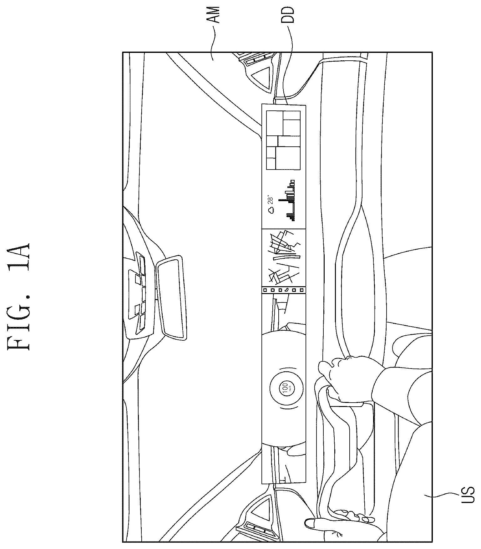
A is a view illustrating an inner structure of a vehicle including a display device according to an embodiment of the present disclosure;
B is a plan view illustrating the display device in A ;
A is a cross-sectional view illustrating the display device according to an embodiment of the present disclosure;
B is a cross-sectional view illustrating a display device according to an embodiment of the present disclosure;
C and 2 D are cross-sectional views obtained by cutting the display device in B along cutting line I-I′ according to embodiments of the present disclosure;
is an exploded perspective view illustrating the display device according to an embodiment of the present disclosure;
is a plan view illustrating an input sensor according to an embodiment of the present disclosure;
A is a waveform diagram representing first to fourth transmission signals according to an embodiment of the present disclosure;
B is a waveform diagram representing first to fourth transmission signals according to an embodiment of the present disclosure;
A is an enlarged plan view illustrating a portion of the input sensor in ;
B is a cross-sectional view taken along line II-II′ in A ;
A is an enlarged plan view illustrating a portion of an input sensor according to an embodiment of the present disclosure;
B is a cross-sectional view taken along line III-III′ in A ;
A is a plan view illustrating an input sensor according to an embodiment of the present disclosure;
B is an enlarged plan view illustrating a first portion in A ;
is a plan view illustrating an input sensor according to an embodiment of the present disclosure;
A is an enlarged plan view illustrating a second portion in ;
B is an enlarged plan view illustrating a third portion in ;
C is a view illustrating an area variation for each position of first sub-dummy patterns according to an embodiment of the present disclosure;
D is a view illustrating an area variation for each position of third sub-dummy patterns according to an embodiment of the present disclosure;
is a plan view illustrating a display device according to an embodiment of the present disclosure; and
is a plan view illustrating an input sensor according to an embodiment of the present disclosure.
DETAILED DESCRIPTION
In this specification, it will be understood that when an element such as a region, layer, or portion is referred to as being “on” another element, it can be directly disposed/connected/coupled on the other element or intervening elements may also be present therebetween.
Like reference numerals refer to like elements throughout. Also, in the figures, the thickness, ratio, and dimensions of components are exaggerated for clarity of illustration. As used herein, the term and/or includes any and all combinations of one or more of the associated listed items.
It will be understood that although the terms such as ‘first’ and ‘second’ are used herein to describe various elements, these elements should not be limited by these terms. The terms are only used to distinguish one component from other components. For example, a first element referred to as a first element in one embodiment can be referred to as a second element in another embodiment without departing from the scope of the appended claims. The terms of a singular form may include plural forms unless referred to the contrary.
Also, spatially relative terms, such as “below”, “lower”, “above”, and “upper”, may be used herein for ease of description to describe an element and/or a feature's relationship to another element(s) and/or feature(s) as illustrated in the drawings. The terms may be a relative concept and described based on directions expressed in the drawings.
The meaning of ‘include’ or ‘comprise’ specifies a property, a fixed number, a step, an operation, an element, a component or a combination thereof, but does not exclude other properties, fixed numbers, steps, operations, elements, components or combinations thereof.
Unless otherwise defined, all terms (including technical and scientific terms) used herein have the same meaning as generally understood by those skilled in the art. Terms as defined in a commonly used dictionary should be construed as having the same meaning as in an associated technical context, and unless defined apparently in the description, the terms are not ideally or excessively construed as having formal meaning.
Hereinafter, embodiments of the present disclosure will be described with reference to the accompanying drawings.
A is a view illustrating an inner structure of a vehicle including a display device according to an embodiment of the present disclosure, and B is a plan view illustrating the display device in A .
Referring to A and 1 B , a display device DD may be activated by an electrical signal. For example, the display device DD may be a large-sized display device used in a television, a monitor, an outdoor advertisement board, or a vehicle AM. However, the embodiment of the present disclosure is not limited thereto. For example, the display device DD may be adopted for a small and medium-sized electronic device such as a personal computer, a notebook computer, a personal digital terminal, a portable electronic device, and a camera. Also, the above-described devices are merely embodiments, and thus, the display device DD may be adopted for other electronic devices unless departing from spirit of an embodiment of the present disclosure. In this embodiment, the display device DD disposed in the vehicle AM is illustrated as an example.
On the display device DD, an active area AA and a peripheral area NAA may be defined. The active area AA may be an area in which pixels are disposed and which substantially displays an image IM. The active area AA may extend long a first direction DR 1 and a second direction DR 2 crossing the first direction DR 1 . Although the active area AA has a rectangular shape as an example in A and 1 B , the shape of the active area AA may be variously changed according to a shape of the display device DD.
The peripheral area NAA may be an area on which the image IM is not displayed. For example, the peripheral area NAA may surround the active area AA. However, the embodiment of the present disclosure is not limited thereto. The peripheral area NAA may be disposed at only one side of the active area AA or omitted.
The display device DD may sense an input generated by using a body (e.g., a finger) of a user US or an input generated by using an input device. The input device may represent a device except for the body of the user US. For example, the input device may include an active pen, a stylus pen, a touch pen, or an electronic pen. The input generated by using the body of the user US may include various types of external inputs such as a touch generated by using a portion of the body of the user US, heat, or a pressure.
A is a cross-sectional view illustrating the display device according to an embodiment of the present disclosure, B is a cross-sectional view illustrating a display device according to an embodiment of the present disclosure, and C and 2 D are cross-sectional views obtained by cutting the display device in B along cutting line I-I′ according to embodiments of the present disclosure.
Referring to A , the display device DD may include a display panel DP and an input sensor ISP. The input sensor ISP may be referred to as an input sensing panel.
The display panel DP may include a first base layer BS 1 , a display circuit layer DP_CL, a display element layer DP_OLED, a second base layer BS 2 , and a coupling member SLM. The input sensor ISP may be disposed on the second base layer BS 2 .
Each of the first base layer BS 1 and the second base layer BS 2 may be a laminated structure including a silicon substrate, a plastic substrate, a glass substrate, an insulation film, or a plurality of insulation layers.
The display circuit layer DP_CL may be disposed on the first base layer BS 1 . The display circuit layer DP_CL may include a plurality of insulation layers, a plurality of conductive layers, and a semiconductor layer. The plurality of conductive layers of the display circuit layer DP_CL may constitute signal lines or a control circuit of a pixel.
The display element layer DP_OLED may be disposed on the display circuit layer DP_CL. The display element layer DP_OLED may include light emitting elements. For example, the display element layer DP_OLED may include an organic light emitting diode, an inorganic light emitting diode, a quantum dot, a quantum rod, a micro-LED, or a nano-LED.
The second base layer BS 2 may be disposed on the display element layer DP_OLED. A predetermined space may be defined between the second base layer BS 2 and the display element layer DP_OLED. That is, both ends of the second base layer BS 2 are supported by the coupling member SLM. The space may be filled with air or an inert gas. Also, in an embodiment of the present disclosure, the space may be filled with a filling layer FL (refer to C ) such as a silicon-based polymer, an epoxy-based resin, or an acrylic-based resin.
A coupling member SLM may be disposed between the first base layer BS 1 and the second base layer BS 2 . The coupling member SLM may couple the first base layer BS 1 and the second base layer BS 2 . The coupling member SLM may include an organic material such as a photo-curable resin or a photo-setting resin or an inorganic material such as a frit seal. However, the embodiment of the present disclosure is not limited thereto.
The input sensor ISP may include a plurality of insulation layers and a plurality of conductive layers. The plurality of conductive layers may constitute sensing electrodes for sensing an external input, sensing lines that are electrically connected with the sensing electrodes, and sensing pads that are electrically connected with the sensing lines.
Referring to B , a display device DD_ 1 may include a display panel DP_ 1 and an input sensor ISP_ 1 . The input sensor ISP_ 1 may be referred to as an input sensing layer.
The display panel DP_ 1 may include a base layer BS, a display circuit layer DP_CL, a display element layer DP_OLED, and an encapsulation layer TFE. The base layer BS may be flexible. The input sensor ISP_ 1 may be disposed on the encapsulation layer TFE. According to an embodiment of the present disclosure, the display panel DP_ 1 and the input sensor ISP_ 1 may be provided through a continuous process. That is, the input sensor ISP_ 1 may be directly provided on the encapsulation layer TFE. However, the embodiment of the present disclosure is not limited thereto.
Referring to A and 2 C , at least one inorganic layer may be provided on a top surface of the first base layer BS 1 in the display panel DP. The inorganic layer may include at least one of an aluminum oxide, a titanium oxide, a silicon oxide, a silicon oxynitride, a silicon nitride, a zirconium oxide, and a hafnium oxide. The inorganic layer may have multiple layers. The multilayered inorganic layers may include a barrier layer and/or a buffer layer. In this embodiment, the display panel DP includes a buffer layer BFL.
The buffer layer BFL may be disposed on the first base layer BS 1 and improve a coupling force between the first base layer BS 1 and a semiconductor pattern. The buffer layer BFL may include a silicon oxide layer and a silicon nitride layer, and the silicon oxide layer and the silicon nitride layer may be alternately laminated with each other.
The semiconductor pattern may be disposed on the buffer layer BFL. The semiconductor pattern may include polysilicon. However, the embodiment of the present disclosure is not limited thereto. For example, the semiconductor pattern may include amorphous silicon, low-temperature polycrystalline silicon, or oxide semiconductor.
C merely illustrates a portion of the semiconductor pattern, and the semiconductor pattern may be further disposed in other areas. The semiconductor pattern may be arranged over pixels according to a particular rule. The semiconductor pattern may have an electrical property that is varied according to whether doped or not. The semiconductor pattern may include a first area having high conductivity and a second area having low conductivity. The first area may be doped with an n-type dopant or a p-type dopant. A p-type transistor may include a doped area that is doped with the p-type dopant, and an n-type transistor may include a doped area that is doped with the n-type dopant. The second area may be an undoped area or a doped area that is doped with a concentration less than that of the first area.
The first area has conductivity greater than that of the second area and substantially serves as an electrode or a signal line. The second area may substantially correspond to a channel region of a transistor. In other words, one portion of the semiconductor pattern may be a channel of a transistor, another portion may be a source or a drain of the transistor, and another portion may be a connection electrode or a connection signal line.
Each of the pixels may have an equivalent circuit including seven transistors, one capacitor, and a light emitting element, and the equivalent circuit of the pixel may be deformed into various shapes. In C , one transistor 100 PC and one light emitting element 100 PE contained in the pixel are illustrated as an example.
The transistor 100 PC may include a source SC 1 , a channel CH 1 , a drain D 1 , and a gate G 1 . The source SC 1 , the channel CH 1 , and the drain D 1 may be provided from the semiconductor pattern. The source SC 1 and the drain D 1 may extend in opposite directions from the channel CH 1 on a cross-section. C illustrates a portion of a connection signal line SCL provided from the semiconductor pattern. Although not shown, the connection signal line SCL may be electrically connected to the drain D 1 of the transistor 100 PC on a plane.
A first insulation layer 10 may be disposed on the buffer layer BFL. The first insulation layer 10 may overlap the plurality of pixels in common and cover the semiconductor pattern. The first insulation layer 10 may be an inorganic layer and/or an organic layer and have a single-layer or multi-layer structure. The first insulation layer 10 may include at least one of an aluminum oxide, a titanium oxide, a silicon oxide, a silicon nitride, a silicon oxynitride, a zirconium oxide, and a hafnium oxide. In this embodiment, the first insulation layer 10 may be a single-layered silicon oxide layer. Also, insulation layers of the display circuit layer DP_CL, which will be described later, may be an inorganic layer and/or an organic layer in addition to the first insulation layer 10 and have a single-layer or multi-layer structure. Although the inorganic layer may include at least one of the above-described materials, the embodiment of the present disclosure is not limited thereto.
The gate G 1 is disposed on the first insulation layer 10 . The gate G 1 may be a portion of a metal pattern. The gate G 1 overlaps the channel CH 1 . The gate G 1 may serve as a mask in a process of doping the semiconductor pattern.
A second insulation layer 20 may be disposed on the first insulation layer 10 to cover the gate G 1 . The second insulation layer 20 may overlap the pixels in common. The second insulation layer 20 may be an inorganic layer and/or an organic layer and have a single-layer or multi-layer structure. The second insulation layer 20 may include at least one of a silicon oxide, a silicon nitride, and a silicon oxynitride. In this embodiment, the second insulation layer 20 may have a multi-layer structure including a silicon oxide layer and a silicon nitride layer.
A third insulation layer 30 may be disposed on the second insulation layer 20 . The third insulation layer 30 may have a single-layer or multi-layer structure. For example, the third insulation layer 30 may have a multi-layer structure including a silicon oxide layer and a silicon nitride layer.
A first connection electrode CNE 1 may be disposed on the third insulation layer 30 . The first connection electrode CNE 1 may be connected to the connection signal line SCL via a contact hole CNT- 1 penetrating through the first, second, and third insulation layers 10 , 20 , and 30 , respectively.
A fourth insulation layer 40 may be disposed on the third insulation layer 30 . The fourth insulation layer 40 may be a single-layered silicon oxide layer. A fifth insulation layer 50 may be disposed on the fourth insulation layer 40 . The fifth insulation layer 50 may be an organic layer.
A second connection electrode CNE 2 may be disposed on the fifth insulation layer 50 . The second connection electrode CNE 2 may be connected to the first connection electrode CNE 1 via a contact hole CNT- 2 penetrating through the fourth and fifth insulation layers 40 and 50 .
A sixth insulation layer 60 may be disposed on the fifth insulation layer 50 to cover the second connection electrode CNE 2 . The sixth insulation layer 60 may be an organic layer.
The display element layer DP_OLED may be disposed on the display circuit layer DP_CL. The display element layer DP_OLED may include a light emitting element 100 PE and a pixel defining layer 70 . For example, the display element layer DP_OLED may include an organic light emitting material, an inorganic light emitting material, a quantum dot, a quantum rod, a micro-LED, or a nano-LED. Hereinafter, although the light emitting element 100 PE will be described as an organic light emitting element as an example, the embodiment of the present disclosure is not limited thereto.
The light emitting element 100 PE may include a first electrode AE, a light emitting layer EL, and a second electrode CE. The first electrode AE may be disposed on the sixth insulation layer 60 . The first electrode AE may be connected to the second connection electrode CNE 2 viaa contact hole CNT- 3 penetrating through the sixth insulation layer 60 .
A pixel defining layer 70 may be disposed on the sixth insulation layer 60 to cover a portion of the first electrode AE. An opening 70 -OP is defined in the pixel defining layer 70 . The opening 70 -OP of the pixel defining layer 70 exposes at least a portion of the first electrode AE.
The active area AA (refer to B ) may include a light emitting area PXA and a non-light emitting area NPXA disposed adjacent to the light emitting area PXA. The non-light emitting area NPXA may surround the light emitting area PXA. In this embodiment, the light emitting area PXA is defined in correspondence to a partial area of the first electrode AE exposed by the opening 70 -OP.
The light emitting layer EL may be disposed on the first electrode AE. The light emitting layer EL may be disposed in an area corresponding to the opening 70 -OP. That is, the light emitting layer EL may be separately provided in each of the pixels. When the light emitting layer EL is separately provided in each of the pixels, each of the light emitting layers EL may emit light having at least one color of blue, red, and green. However, the embodiment of the present disclosure is not limited thereto. For example, the light emitting layer EL may be connected to the pixels and provided in common. In this case, the light emitting layer EL may provide blue light or white light.
The second electrode CE may be disposed on the light emitting layer EL. The second electrode CE may have an integrated shape and be disposed on the plurality of pixels in common.
Although not shown, a hole control layer may be disposed between the first electrode AE and the light emitting layer EL. The hole control layer may be disposed on the light emitting area PXA and the non-light emitting area NPXA in common. The hole control layer may include a hole transport layer and further include a hole injection layer. An electron control layer may be disposed between the light emitting layer EL and the second electrode CE. The electron control layer may include an electron transport layer and further include an electron injection layer. The hole control layer and the electron control layer may be provided to the plurality of pixels in common by using an open mask.
The second base layer BS 2 may be disposed on the display element layer DP_OLED. In an embodiment of the present disclosure, each of the first and second base layers BS 1 and BS 2 may be rigid.
The filling layer FL may be disposed between the first and second base layers BS 1 and BS 2 . The filling layer FL may be disposed in a space sealed by the coupling member SLM (refer to A ) disposed between the first and second base layers BS 1 and BS 2 . The filling layer FL may include a thermosetting material.
The input sensor ISP may be directly disposed on the display panel DP. For example, the input sensor ISP may be directly disposed on the second base layer BS 2 without any bonding layer.
Referring to B and 2 D , the encapsulation layer TFE may be disposed on the display element layer DP_OLED. Although the encapsulation layer TFE may include an inorganic layer, an organic layer, and an inorganic layer, which are sequentially laminated, the embodiment of the present disclosure is not limited to the layers of the encapsulation layer TFE.
The inorganic layers may protect the display element layer DP_OLED from moisture and oxygen, and the organic layer may protect the light emitting element layer DP_OLED from foreign substances such as dust particles. The inorganic layers may include a silicon nitride layer, a silicon oxynitride layer, a silicon oxide layer, a titanium oxide layer, or an aluminum oxide layer. Although the organic layer may include an acrylic-based organic layer, the embodiment of the present disclosure is not limited thereto.
The input sensor ISP_ 1 may be provided on the display panel DP_ 1 through a continuous process. In this case, the input sensor ISP_ 1 may be directly disposed on the display panel DP_ 1 . For example, a feature of being “directly disposed” may represent that a third component is not disposed between the input sensor ISP_ 1 and the display panel DP_ 1 . That is, a separate adhesive or coupling member may not be disposed between the input sensor ISP_ 1 and the display panel DP_ 1 . Alternatively, the input sensor ISP_ 1 may be coupled to the display panel DP_ 1 through an adhesive member or a coupling member. The adhesive member may include a typical adhesive or a typical sticking agent.
Referring to C and 2 D , the input sensor ISP and ISP_ 1 may include a base insulation layer 201 , a first conductive layer 202 , a sensing insulation layer 203 , a second conductive layer 204 , and a cover insulation layer 205 . The base insulation layer 201 , the first conductive layer 202 , the sensing insulation layer 203 , the second conductive layer 204 , and the cover insulation layer 205 are sequentially stacked in the third direction DR 3 . As depicted in C , the first conductive layer 202 and the second conductive layer 204 overlap the light emitting area PXA and the non-light emitting area NPXA. However, as depicted in D , the first conductive layer 202 and the second conductive layer 204 overlap the non-light emitting area NPXA and do not overlap the light emitting area PXA.
The base insulation layer 201 may be an inorganic layer including one of a silicon nitride, a silicon oxynitride, and a silicon oxide. Alternatively, the base insulation layer 201 may be an organic layer including an epoxy resin, an acrylic resin, or imide-based resin. The base insulation layer 201 may have a single-layer structure or a multi-layer structure laminated in the third direction DR 3 .
Each of the first conductive layer 202 and the second conductive layer 204 may have a single-layer structure or a multi-layer structure laminated in the third direction DR 3 .
The single-layered conductive layer may include a metal layer or a transparent conductive layer. The metal layer may include molybdenum, silver, titanium, copper, aluminum, and an alloy thereof. The transparent conductive layer may include a transparent conductive oxide such as an indium tin oxide (ITO), an indium zinc oxide (IZO), a zinc oxide (ZnO), and an indium zinc tin oxide (IZTO). In addition, the transparent conductive layer may include a conductive polymer such as PEDOT, a metal nano-wire, or a graphene.
The multi-layered conductive layer may include metal layers. The metal layers may have, e.g., a three-layer structure of titanium/aluminum/titanium. The multi-layered conductive layer may include at least one metal layer and at least one transparent conductive layer.
At least one of the sensing insulation layer 203 and the cover insulation layer 205 may include an inorganic layer. The inorganic layer may include at least one of an aluminum oxide, a titanium oxide, a silicon oxide, a silicon nitride, a silicon oxynitride, a zirconium oxide, and a hafnium oxide.
At least one of the sensing insulation layer 203 and the cover insulation layer 205 may include an organic layer. The organic layer may include at least one of an acrylic-based resin, a methacrylic-based resin, a polyisoprene-based resin, a vinyl-based resin, an epoxy-based resin, a urethane-based resin, a cellulose-based resin, a siloxane-based resin, a polyimide-based resin, a polyamide-based resin, or a perylene-based resin.
is an exploded perspective view illustrating the display device according to an embodiment of the present disclosure.
Referring to , the display device DD may include a display panel DP and an input sensor ISP.
The display panel DP may be a component that substantially generates an image. The display panel DP may be a light emitting display panel. For example, the display panel DP may be an organic light emitting display panel, a quantum dot display panel, a micro-LED display panel, or a nano-LED display panel.
The display panel DP includes a display area DA for displaying the image IM (refer to B ) and a non-display area NDA disposed adjacent to the display area DA. The display area DA may correspond to the active area AA illustrated in B , and the non-display area NDA may correspond to the peripheral area NAA illustrated in B . The display area DA may be an area that substantially displays an image, and the non-display area NDA may be a bezel area on which an image is not displayed. Although the non-display area NDA surrounds the display area DA in , the embodiment of the present disclosure is not limited thereto. The non-display area NDA may be disposed at only at least one side of the display area DA.
The display panel DP includes a plurality of pixels PX and signal lines connected to the plurality of pixels PX. Each of the plurality of pixels PX may include a light emitting element. The signal lines may include data lines, scan lines, and power lines.
The input sensor ISP may be disposed on the display panel DP. The input sensor ISP may sense an external input applied from the outside. In an embodiment of the present disclosure, the input sensor ISP may overlap the display area DA. The input sensor ISP may include a plurality of areas. Although the input sensor ISP is divided into two areas by a virtual boundary line BL as an example in , the embodiment of the present disclosure is not limited to the number of the areas of the input sensor ISP. Hereinafter, the two areas are referred to as a first sensing area SA 1 and a second sensing area SA 2 , respectively. The first and second sensing areas SA 1 and SA 2 are adjacent to each other in the second direction DR 2 .
The display device DD may further include a plurality of data driving chips DIC 1 , DC 2 , DC 3 , and DIC 4 , a plurality of flexible films COF 1 , COF 2 , COF 3 , and COF 4 , and a printed circuit board PCB. The plurality of flexible films COF 1 , COF 2 , COF 3 , and COF 4 may be disposed between the display panel DP and the printed circuit board PCB to electrically connect the display panel DP and the printed circuit board PCB. Each of the flexible films COF 1 , COF 2 , COF 3 , and COF 4 has one end coupled to the display panel DP and the other end coupled to the printed circuit board PCB.
Although the data driving chips DIC 1 , DC 2 , DC 3 , and DIC 4 are mounted to the flexible films COF 1 , COF 2 , COF 3 , and COF 4 , respectively, in , the embodiment of the present disclosure is not limited thereto. That is, the data driving chips DIC 1 , DC 2 , DC 3 , and DIC 4 may be directly mounted onto the display panel DP through a chip on glass (COG) method.
All sorts of circuits for generating all sorts of control signals and power signals, which are necessary for driving the display panel DP and the data driving chips DIC 1 , DC 2 , DC 3 , and DIC 4 , may be provided on the printed circuit board PCB. In an embodiment of the present disclosure, a main controller MCU may be mounted onto the printed circuit board PCB to control an overall operation of the display device DD. For example, the main controller MCU may include at least one microprocessor. The main controller MCU may be referred to as a host. The main controller MCU may further include a graphic controller.
The display device DD may further include a first sensor controller TIC 1 and a second sensor controller TIC 2 for controlling driving of the input sensor ISP. Although two sensor controllers TIC 1 and TIC 2 are illustrated as an embodiment of the present disclosure, the embodiment of the present disclosure is not limited thereto, and the number of the sensor controllers may be varied. For example, when the display device DD increases in size, the number of the sensor controllers TIC 1 and TIC 2 may further increase.
The first sensor controller TIC 1 may control driving of the first sensing area SA 1 of the input sensor ISP, and the second sensor controller TIC 2 may control driving of the second sensing area SA 2 of the input sensor ISP. Each of the first and second sensor controllers TIC 1 and TIC 2 may have a chip shape and be mounted onto the printed circuit board PCB.
The first and second sensor controllers TIC 1 and TIC 2 may receive a sensing control signal or the like from the main controller MCU. The sensing control signal may include a clock signal or a mode determination signal for determining a driving mode (or sensing mode) of the first and second sensor controllers TIC 1 and TIC 2 . The first and second sensor controllers TIC 1 and TIC 2 may provide transmission signals that will be described later to the input sensor ISP based on the sensing control signal.
The first and second sensor controllers TIC 1 and TIC 2 may calculate coordinate information of an input based on reception signals received from the input sensor ISP and provide a coordinate signal having the coordinate information to the main controller MCU. The main controller MCU executes an operation corresponding to the input based on the coordinate signal. For example, the main controller MCU may operate the display panel DP to display a new image on the display panel DP based on the coordinate signal.
is a plan view illustrating the input sensor according to an embodiment of the present disclosure, A is a waveform diagram representing first to fourth transmission signals according to an embodiment of the present disclosure, and B is a waveform diagram representing first to fourth transmission signals according to an embodiment of the present disclosure.
Referring to , 5 A, and 5 B , the input sensor ISP includes a first sensing area SA 1 and a second sensing area SA 2 . The first sensing area SA 1 and the second sensing area SA 2 may be adjacent to each other in the second direction DR 2 . Although the input sensor ISP includes two sensing areas SA 1 and SA 2 , the embodiment of the present disclosure is not limited thereto. Alternatively, the input sensor ISP may include one sensing area or three or more sensing areas.
The first sensing area SA 1 includes a first sub-area SSA 1 and a second sub-area SSA 2 . The first and second sub-area SSA 1 and SSA 2 may be adjacent to each other in the first direction DR 1 . The second sensing area SA 2 includes a third sub-area SSA 3 and a fourth sub-area SSA 4 . The third and fourth sub-area SSA 3 and SSA 4 may be adjacent to each other in the first direction DR 1 .
The input sensor ISP may include first sensing electrodes TE 1 , second sensing electrodes RE 1 , third sensing electrodes TE 2 , and fourth sensing electrodes RE 2 . The first sensing electrodes TE 1 are disposed in the first sub-area SSA 1 and receive a first transmission signal TS 1 from the first sensor controller TIC 1 . The second sensing electrodes RE 1 are disposed in the first sub-area SSA 1 and intersect with the first sensing electrodes TE 1 . The first sensing electrodes TE 1 may each extend in the first direction DR 1 and be arranged in the second direction DR 2 . The second sensing electrodes RE 1 may each extend in the second direction DR 2 and be arranged in the first direction DR 1 . The third sensing electrodes TE 2 are disposed in the second sub-area SSA 2 and receive a second transmission signal TS 2 from the first sensor controller TIC 1 . The second transmission signal TS 2 may have a phase inverted from that of the first transmission signal TS 1 . The fourth sensing electrodes RE 2 are disposed in the second sub-area SSA 2 and intersect with the third sensing electrodes TE 2 . The third sensing electrodes TE 2 may each extend in the first direction DR 1 and be arranged in the second direction DR 2 . The fourth sensing electrodes RE 2 may each extend in the second direction DR 2 and be arranged in the first direction DR 1 .
The first sensing electrodes TE 1 may be referred to as first transmission electrodes, and the third sensing electrodes TE 2 may be referred to as second transmission electrodes. Also, the second sensing electrodes RE 1 may be referred to as first reception electrodes, and the fourth sensing electrodes RE 2 may be referred to as second reception electrodes.
The number of the first sensing electrodes TE 1 disposed in the first sub-area SSA 1 is equal to that of the third sensing electrodes TE 2 disposed in the second sub-area SSA 2 . The number of the second sensing electrodes RE 1 disposed in the first sub-area SSA 1 is equal to that of the fourth sensing electrodes RE 2 disposed in the second sub-area SSA 2 . Although seven first sensing electrodes TE 1 are disposed in the first sub-area SSA 1 , and seven third sensing electrodes TE 2 are disposed in the second sub-area SSA 2 as an example in , the embodiment of the present disclosure is not limited to the number of each of the first and third sensing electrodes TE 1 and TE 2 . Although four second sensing electrodes RE 1 are disposed in the first sub-area SSA 1 , and four fourth sensing electrodes RE 2 are disposed in the second sub-area SSA 2 as an example in , the embodiment of the present disclosure is not limited to the number of each of the second and fourth sensing electrodes RE 1 and RE 2 .
A length in the first direction DR 1 of each of the first sensing electrodes TE 1 may be substantially equal to that in the first direction DR 1 of each of the third sensing electrodes TE 2 . Specifically, the first sensing electrode disposed in a first column among the first sensing electrodes TE 1 and the third sensing electrode disposed in a first column among the third sensing electrodes TE 2 may have the same length as each other. That is, the first and third sensing electrodes TEL and TE 2 disposed at the same column may have the same length as each other.
In an embodiment of the present disclosure, the first sensing electrodes TE 1 and the third sensing electrodes TE 2 may have symmetric shapes based on a boundary between the first and second sub-areas SSA 1 and SSA 2 . The first sensing electrodes TE 1 and the third sensing electrodes TE 2 may be spaced apart from the boundary between the first and second sub-areas SSA 1 and SSA 2 . The first sensing electrodes TE 1 and the third sensing electrodes TE 2 may be electrically insulated from each other.
A second boundary sensing electrode disposed adjacent to the boundary between the first and second sub-areas SSA 1 and SSA 2 among the second sensing electrodes RE 1 may have a different area (e.g., a half area) from the rest second sensing electrodes. A fourth boundary sensing electrode disposed adjacent to the boundary between the first and second sub-areas SSA 1 and SSA 2 among the fourth sensing electrodes RE 2 may have a different area (e.g., a half area) from the rest second sensing electrodes. However, the embodiment of the present disclosure is not limited thereto. For example, the second boundary sensing electrode may have the same area as the rest second sensing electrodes, and the fourth boundary sensing electrode may also have the same area as the rest fourth sensing electrodes.
The input sensor ISP includes first transmission lines TL 1 a , TL 2 a , TL 3 a , TL 4 a , TL 5 a , TL 6 a , and TL 7 a , first reception lines RL 1 a , RL 2 , RL 3 , and RL 4 a , second transmission lines TL 1 b , TL 2 b , TL 3 b , TL 4 b , TL 5 b , TL 6 b , and TL 7 b , and second reception lines RL 1 b , RL 2 b , RL 3 b , and RL 4 b . The first transmission lines TL 1 a , TL 2 a , TL 3 a , TL 4 a , TL 5 a , TL 6 a , and TL 7 a , the first reception lines RL 1 a , RL 2 a , RL 3 a , and RL 4 a , the second transmission lines TL 1 b , TL 2 b , TL 3 b , TL 4 b , TL 5 b . TL 6 b , and TL 7 b , and second reception lines RL 1 b , RL 2 b , RL 3 b , and RL 4 b may be disposed in correspondence to the non-display area NDA (refer to ) of the display panel DP (refer to ).
Each of the first transmission lines TL 1 a , TL 2 a , TL 3 a , TL 4 a , TL 5 a , TL 6 a , and TL 7 a are connected to the first sensing electrodes TE 1 , and each of the first reception lines RL 1 a , RL 2 , RL 3 , and RL 4 a are connected to the second sensing electrodes RE 1 . Each of the second transmission lines TL 1 b , TL 2 b , TL 3 b , TL 4 b , TL 5 b , TL 6 b , and TL 7 b are connected to the third sensing electrodes TE 2 , and each of the second reception lines RL 1 b , RL 2 b , RL 3 b , and RL 4 b are connected to the fourth sensing electrodes RE 2 .
The first transmission lines TL 1 a , TL 2 a , TL 3 a , TL 4 a , TL 5 a , TL 6 a , and TL 7 a receive the first transmission signal TS 1 from the first sensor controller TIC 1 and provide the first transmission signal TS 1 to the first sensing electrodes TE 1 . The second transmission lines TL 1 b , TL 2 b , TL 3 b , TL 4 b , TL 5 b , TL 6 b , and TL 7 b receive the second transmission signal TS 2 from the first sensor controller TIC 1 and provide the second transmission signal TS 2 to the third sensing electrodes TE 2 .
The first sensor controller TIC 1 includes a first data acquisition part AFE 1 for receiving a first reception signal from the second sensing electrodes RE 1 and a second data acquisition part AFE 2 for receiving a second reception signal from the fourth sensing electrodes RE 2 . The first data acquisition part AFE 1 receives the first reception signal through the first reception lines RL 1 a , RL 2 a , RL 3 a , and RL 4 a , and the second data acquisition part AFE 2 receives the second reception signal through the second reception lines RL 1 b , RL 2 b , RL 3 b , and RL 4 b.
The first sensor controller TIC 1 may sense a variation of capacitance (hereinafter, referred to as mutual capacitance) between the first and second sensing electrodes TE 1 and RE 1 in the first sub-area SSA 1 based on the first reception signal and generate coordinate information of a position at which the variation is sensed. The first sensor controller TIC 1 may sense a variation of mutual capacitance between the third and fourth sensing electrodes TE 2 and RE 2 in the second sub-area SSA 2 based on the second reception signal and generate coordinate information of a position at which the variation is sensed.
The input sensor ISP may further include fifth sensing electrodes TE 3 , sixth sensing electrodes RE 3 , seventh sensing electrodes TE 4 , and eighth sensing electrodes RE 4 . The fifth sensing electrodes TE 3 are disposed in the third sub-area SSA 3 and receive a third transmission signal TS 3 from the second sensor controller TIC 2 . The sixth sensing electrodes RE 3 are disposed in the third sub-area SSA 3 and intersect with the fifth sensing electrodes TE 3 . The fifth sensing electrodes TE 3 may each extend in the first direction DR 1 and be arranged in the second direction DR 2 . The sixth sensing electrodes RE 3 may each extend in the second direction DR 2 and be arranged in the first direction DR 1 . The seventh sensing electrodes TE 4 are disposed in the fourth sub-area SSA 4 and receive a fourth transmission signal TS 4 from the second sensor controller TIC 2 . The fourth transmission signal TS 4 may have a phase inverted from that of the third transmission signal TS 3 . The eighth sensing electrodes RE 4 are disposed in the fourth sub-area SSA 4 and intersect with the seventh sensing electrodes TE 4 . The seventh sensing electrodes TE 3 may each extend in the first direction DR 1 and be arranged in the second direction DR 2 . The eighth sensing electrodes RE 4 may each extend in the second direction DR 2 and be arranged in the first direction DR 1 .
The fifth sensing electrodes TE 3 may be referred to as third transmission electrodes, and the seventh sensing electrodes TE 4 may be referred to as fourth transmission electrodes. Also, the sixth sensing electrodes RE 3 may be referred to as third reception electrodes, and the eighth sensing electrodes RE 4 may be referred to as fourth reception electrodes.
The number of the fifth sensing electrodes TE 3 disposed in the third sub-area SSA 3 is equal to that of the seventh sensing electrodes TE 4 disposed in the fourth sub-area SSA 4 . The number of the sixth sensing electrodes RE 3 disposed in the third sub-area SSA 3 is equal to that of the eighth sensing electrodes RE 4 disposed in the fourth sub-area SSA 4 . The third sub-area SSA 3 is adjacent to the first sub-area SSA 1 in the second direction DR 2 , and the fourth sub-area SSA 4 is adjacent to the second sub-area SSA 2 in the second direction DR 2 . The number of the fifth sensing electrodes TE 3 may be equal to that of the first sensing electrodes TE 1 , and the number of the seventh sensing electrodes TE 4 may be equal to that of the third sensing electrodes TE 2 .
Although seven fifth sensing electrodes TE 3 are disposed in the third sub-area SSA 3 , and seven seventh sensing electrodes TE 4 are disposed in the fourth sub-area SSA 4 as an example in , the embodiment of the present disclosure is not limited to the number of each of the fifth and seventh sensing electrodes TE 3 and TE 4 . Although four sixth sensing electrodes RE 3 are disposed in the third sub-area SSA 3 , and four eighth sensing electrodes RE 4 are disposed in the fourth sub-area SSA 4 as an example in , the embodiment of the present disclosure is not limited to the number of each of the sixth and eighth sensing electrodes RE 3 and RE 4 .
A length in the first direction DR 1 of each of the fifth sensing electrodes TE 3 may be substantially equal to that in the first direction DR 1 of each of the seventh sensing electrodes TE 4 . Specifically, the fifth sensing electrode disposed in a first column among the fifth sensing electrodes TE 3 and the seventh sensing electrode disposed in a first column among the seventh sensing electrodes TE 4 may have the same length as each other. That is, the fifth and seventh sensing electrodes TE 3 and TE 4 disposed at the same column may have the same length as each other.
In an embodiment of the present disclosure, the fifth sensing electrodes TE 3 and the seventh sensing electrodes TE 4 may have symmetric shapes based on a boundary between the third and fourth sub-areas SSA 3 and SSA 4 . The fifth sensing electrodes TE 3 and the seventh sensing electrodes TE 4 may be spaced apart from the boundary between the third and fourth sub-areas SSA 3 and SSA 4 . The fifth sensing electrodes TE 3 and the seventh sensing electrodes TE 4 may be electrically insulated from each other. In an embodiment of the present disclosure, the first sensing electrodes TE 1 and fifth sensing electrodes TE 3 may have symmetric shapes based on a boundary between the first and third sub-areas SSA 1 and SSA 3 . In an embodiment of the present disclosure, the third sensing electrodes TE 2 and the seventh sensing electrodes TE 4 may have symmetric shapes based on a boundary between the second and fourth sub-areas SSA 2 and SSA 4 .
The input sensor ISP further includes third transmission lines TL 8 a , TL 9 a , TL 10 a , TL 11 a , Tl 12 a , Tl 13 a , and TL 14 a , third reception lines RL 1 c , RL 2 c , RL 3 c , and RL 4 c , fourth transmission lines TL 8 b , TL 9 b , TL 10 b , TL 11 b , TL 12 b , TL 13 b , and TL 14 b , and fourth reception lines RL 1 d , RL 2 d , RL 3 d , and RL 4 d . The third transmission lines TL 8 a , TL 9 a , TL 10 a , TL 11 a , Tl 12 a , Tl 13 a , and TL 14 a , the third reception lines RL 1 c , RL 2 c , RL 3 c , and RL 4 c , the fourth transmission lines TL 8 b , TL 9 b , TL 10 b , TL 11 b , TL 12 b , TL 13 b , and TL 14 b , and the fourth reception lines RL 1 d , RL 2 d , RL 3 d , and RL 4 d may be disposed in correspondence to the non-display area NDA of the display panel DP.
Each of the third transmission lines TL 8 a , TL 9 a , TL 10 a , TL 11 a , Tl 12 a , Tl 13 a , and TL 14 a are connected to the fifth sensing electrodes TE 3 , and each of the third reception lines RL 1 c , RL 2 c , RL 3 c , and RL 4 c are connected to the sixth sensing electrodes RE 3 . Each of the fourth transmission lines TL 8 b , TL 9 b , TL 10 b , TL 11 b , TL 12 b , TL 13 b , and TL 14 b are connected to the seventh sensing electrodes TE 4 , and each of the fourth reception lines RL 1 d , RL 2 d , RL 3 d , and RL 4 d are connected to the eighth sensing electrodes RE 4 .
The third transmission lines TL 8 a , TL 9 a , TL 10 a , TL 11 a , Tl 12 a , Tl 13 a , and TL 14 a receive the third transmission signal TS 3 from the second sensor controller TIC 2 and provide the third transmission signal TS 3 to the fifth sensing electrodes TE 3 . The fourth transmission lines TL 8 b , TL 9 b , TL 10 b , TL 11 b , TL 12 b , TL 13 b , and TL 14 b receive the fourth transmission signal TS 4 from the second sensor controller TIC 2 and provide the fourth transmission signal TS 4 to the seventh sensing electrodes TE 4 .
The second sensor controller TIC 2 includes a third data acquisition part AFE 3 for receiving a third reception signal from the sixth sensing electrodes RE 3 and a fourth data acquisition part AFE 4 for receiving a fourth reception signal from the eighth sensing electrodes RE 4 . The third data acquisition part AFE 3 receives the third reception signal through the third reception lines RL 1 c to RL 4 c , and the fourth data acquisition part AFE 4 receives the fourth reception signal through the second reception lines RL 1 d , RL 2 d , RL 3 d , and RL 4 d.
The second sensor controller TIC 2 may sense a variation of mutual capacitance between the fifth and sixth sensing electrodes TE 3 and RE 3 caused by an external input in the third sub-area SSA 3 based on the third reception signal and generate coordinate information of a position at which the variation is sensed. The second sensor controller TIC 2 may sense a variation of mutual capacitance between the seventh and eighth sensing electrodes TE 4 and RE 4 in the fourth sub-area SSA 4 based on the third reception signal and generate coordinate information of a position at which the variation is sensed.
Referring to A , the first transmission signal TS 1 provided from the first sensing electrodes TE 1 may be a square wave signal that swings with a first amplitude Va 1 . The second transmission signal TS 2 provided from the third sensing electrodes TE 2 may be a square wave signal that swings with a second amplitude Va 2 . The second transmission signal TS 2 may have a phase inverted from that of the first transmission signal TS 1 . In an embodiment of the present disclosure, the second amplitude Va 2 of the second transmission signal TS 2 may be equal to the first amplitude Va 1 of the first transmission signal TS 1 .
The third transmission signal TS 3 provided from the fifth sensing electrodes TE 3 may be a square wave signal that swings with a third amplitude Va 3 . The fourth transmission signal TS 4 provided from the seventh sensing electrodes TE 4 may be a square wave signal that swings with a fourth amplitude Va 4 . The fourth transmission signal TS 4 may have a phase inverted from that of the third transmission signal TS 3 . In an embodiment of the present disclosure, the fourth amplitude Va 4 of the fourth transmission signal TS 4 may be equal to the third amplitude Va 3 of the third transmission signal TS 3 . However, the embodiment of the present disclosure is not limited thereto.
Although not shown, in an embodiment of the present disclosure, the first transmission signal TS 1 may have a phase inverted from that of the third transmission signal TS 3 , and the second transmission signal TS 2 may have a phase inverted from that of the fourth transmission signal TS 4 . The first amplitude Va 1 of the first transmission signal TS 1 may be equal to the third amplitude Va 3 of the third transmission signal TS 3 , and the second amplitude Va 2 of the second transmission signal TS 2 may be equal to the fourth amplitude Va 4 of the fourth transmission signal TS 4 .
When the first transmission signal TS 1 is provided to the first sub-area SSA 1 , and the second transmission signal TS 2 having the phase inverted from that of the first transmission signal TS 1 is provided to the second sub-area SSA 2 , destructive interference may be generated between the first and second transmission signals TS 1 and TS 2 . When the destructive interference is generated between the first and second transmission signals TS 1 and TS 2 , electro-magnetic interference (EMI) may be improved in comparison with a case when the first and second transmission signals TS 1 and TS 2 are transmitted with the same phase.
Also, the first transmission signal TS 1 provided to the first sub-area SSA 1 has a phase inverted from that of the third transmission signal TS 3 provided to the third sub-area SSA 3 . Thus, the destructive interference may be also generated between the first and third transmission signals TS 1 and TS 3 . Likewise, the second transmission signal TS 2 provided to the second sub-area SSA 2 has a phase inverted from that of the fourth transmission signal TS 4 provided to the fourth sub-area SSA 4 . Thus, the destructive interference may be also generated between the second and fourth transmission signals TS 2 and TS 4 . As the destructive interference is generated between adjacent sub-areas SSA 1 to SSA 4 , the electro-magnetic interference (EMI) may be further improved.
Referring to B , a second amplitude Va 2 of a second transmission signal TS 2 may be different from a first amplitude Va 11 of a first transmission signal TS 1 a . For example, the first amplitude Va 11 of the first transmission signal TS 1 a may be greater than the second amplitude Va 2 of the second transmission signal TS 2 . An amplitude difference between the first transmission signal TS 1 a and the second transmission signal TS 2 may be set according to a line resistance difference between the first transmission lines TL 1 a , TL 2 a , TL 3 a , TL 4 a , TL 5 a , TL 6 a , and TL 7 a and the second transmission lines TL 1 b , TL 2 b , TL 3 b , TL 4 b , TL 5 b , TL 6 b , and TL 7 b . Thus, the destructive interference may be effectively generated by only adjusting the amplitude of the first and second transmission signals TS 1 a and TS 2 instead of performing an equivalent resistance design for compensating the line resistance difference between the first transmission lines TL 1 a , TL 2 a , TL 3 a , TL 4 a , TL 5 a , TL 6 a , and TL 7 a and the second transmission lines TL 1 b , TL 2 b , TL 3 b , TL 4 b , TL 5 b , TL 6 b , and TL 7 b.
Also, a fourth amplitude Va 4 of a fourth transmission signal TS 4 may be different from a third amplitude Va 31 of a third transmission signal TS 3 a . For example, the third amplitude Va 31 of the third transmission signal TS 3 a may be greater than the fourth amplitude Va 4 of the fourth transmission signal TS 4 . An amplitude difference between the third transmission signal TS 3 a and the fourth transmission signal TS 4 may be set according to a line resistance difference between the third transmission lines TL 8 a , TL 9 a , TL 10 a , TL 11 a , TL 12 a , TL 13 a , and TL 14 a and the fourth transmission lines TL 8 b , TL 9 b , TL 10 b , TL 11 b , TL 12 b , TL 13 b , and TL 14 b . Thus, the destructive interference may be effectively generated by only adjusting the amplitude of the third and fourth transmission signals TS 3 a and TS 4 instead of performing an equivalent resistance design for compensating the line resistance difference between the third transmission lines TL 8 a , TL 9 a , TL 10 a , TL 11 a , TL 12 a , TL 13 a , and TL 14 a and the fourth transmission lines TL 8 b , TL 9 b , TL 10 b , TL 11 b , TL 12 b , TL 13 b , and TL 14 b.
A is an enlarged plan view illustrating a portion of the input sensor in , and B is a cross-sectional view taken along line II-II′ in A . A is an enlarged plan view illustrating a portion of an input sensor according to an embodiment of the present disclosure, and B is a cross-sectional view taken along line III-III′ in A .
Referring to A and 6 B , each of the first sensing electrodes TE 1 may include a plurality of first sensing patterns TP 1 and a plurality of first bridge patterns BP 1 , which are arranged in the first direction DR 1 . At least one first bridge pattern BP 1 may be connected to two adjacent first sensing patterns TP 1
A sensing insulation layer 203 may be disposed between the plurality of first sensing patterns TP 1 and the plurality of first bridge patterns BP 1 , and each of the plurality of first bridge patterns BP 1 may be connected to the corresponding first sensing patterns TP 1 through contact holes TP_CH defined in the sensing insulation layer 203 .
Each of the second sensing electrodes RE 1 may include a plurality of second sensing patterns RP 1 and a plurality of first extension patterns EP 1 , which are arranged in the second direction DR 2 . At least one first extension pattern EP 1 may be connected between two adjacent second sensing patterns RP 1 . The first extension pattern EP 1 may be integrated with two adjacent second sensing patterns RP 1 . The first extension patterns EP 1 may be insulated from the first bridge patterns BP 1 and intersect with the first bridge patterns BP 1 .
The first and second sensing patterns TP 1 and RP 1 and the first extension patterns EP 1 may be disposed on the same layer (e.g., the sensing insulation layer 203 ). The first bridge patterns BP 1 may be disposed on a layer (e.g., the base insulation layer 201 ) different from the sensing insulation layer 203 .
In an embodiment of the present disclosure, the first and second sensing patterns TP 1 and RP 1 and the first extension patterns EP 1 may be included in the second conductive layer 204 in C , and the first bridge patterns BP 1 may be included in the first conductive layer 202 in C .
In an embodiment of the present disclosure, each of the first and second sensing patterns TP 1 and RP 1 , the first extension patterns EP 1 , and the first bridge patterns BP 1 may include a transparent conductive layer. Each of the first and second sensing patterns TP 1 and RP 1 may have a size for covering the plurality of light emitting elements 100 PE (refer to C ).
Referring to A and 7 B , as an embodiment of the present disclosure, each of first and second sensing patterns TPa and RPa, first extension patterns EPa, and first bridge patterns BPa may include a metal layer. Each of the first and second sensing patterns TPa and RPa, the first extension patterns EPa, and the first bridge patterns BPa may have a mesh shape. Each of the plurality of first bridge patterns BPa may be connected to the corresponding first sensing patterns TPa through contact holes TP_CHa defined in the sensing insulation layer 203 .
Thus, touch openings TOP may be defined in each of the first and second sensing patterns TPa and RPa. In an embodiment of the present disclosure, each of the touch openings TOP may have a rhombus shape.
When viewed on a plane, the plurality of light emitting elements 100 PE (refer to D ) may be disposed in the touch openings TOP, respectively.
Thus, light generated by the light emitting elements 100 PE may be emitted normally instead of being affected by the first and second sensing patterns TPa and RPa.
A is a plan view illustrating an input sensor according to an embodiment of the present disclosure, and B is an enlarged plan view illustrating a first portion BB 1 in A . In A , the same components as those of will be designated by the same reference numerals, and overlapped descriptions thereof will be omitted.
Referring to A and 8 B , an input sensor ISPa includes a first sensing area SA 1 a and a second sensing area SA 2 a . The first sensing area SA 1 a and the second sensing area SA 2 a may be adjacent to each other in the second direction DR 2 .
The first sensing area SA 1 a includes a first sub-area SSA 1 a and a second sub-area SSA 2 a . The first and second sub-area SSA 1 a and SSA 2 a may be adjacent to each other in the first direction DR 1 . The second sensing area SA 2 a includes a third sub-area SSA 3 a and a fourth sub-area SSA 4 a . The third and fourth sub-area SSA 1 a and SSA 2 a may be adjacent to each other in the first direction DR 1 .
The input sensor ISPa may include first sensing electrodes TE 1 , second sensing electrodes RE 1 , third sensing electrodes TE 2 , and fourth sensing electrodes RE 2 .
Each of the first sensing electrodes TE 1 may include a plurality of first sensing patterns TP 1 and a plurality of first bridge patterns BP 1 , which are arranged in the first direction DR 1 . At least one first bridge pattern BP 1 may be connected between two adjacent first sensing patterns TP 1 . Each of the second sensing electrodes RE 1 may include a plurality of second sensing patterns RP 1 and a plurality of first extension patterns EP 1 , which are arranged in the second direction DR 2 . At least one first extension pattern EP 1 may be connected between two adjacent second sensing patterns RP 1 .
Each of the third sensing electrodes TE 2 may include a plurality of third sensing patterns TP 2 and a plurality of second bridge patterns BP 2 , which are arranged in the first direction DR 1 . At least one second bridge pattern BP 2 may be connected between two adjacent third sensing patterns TP 2 . Each of the fourth sensing electrodes RE 2 may include a plurality of fourth sensing patterns RP 2 and a plurality of second extension patterns EP 2 , which are arranged in the second direction DR 2 . At least one second extension pattern EP 2 may be connected between from two adjacent fourth sensing patterns RP 2 .
The first sensing electrodes TE 1 and third sensing electrodes TE 2 may have asymmetric shapes based on a boundary between the first and second sub-areas SSA 1 a and SSA 2 a . A length in the first direction DR 1 of each of the first sensing electrodes TE 1 may be different from that in the first direction DR 1 of each of the third sensing electrodes TE 2 . Specifically, the first sensing electrode TE 1 disposed at a last column (e.g., a seventh column) among the first sensing electrodes TE 1 may have a length less than that of the third sensing electrode TE 2 disposed at the last column among the third sensing electrodes TE 2 . That is, the first and third sensing electrodes TE 1 and TE 2 disposed at the same column may have different lengths from each other. A length difference between the first sensing electrode TE 1 and the third sensing electrode TE 2 may be set according to a line resistance difference between first transmission lines TL 1 a , TL 2 a , TL 3 a , TL 4 a , TL 5 a , TL 6 , and to TL 7 a and second transmission lines TL 1 b , TL 2 b , TL 3 b , TL 4 b , TL 5 b , TL 6 b , and TL 7 b.
The first sensing patterns (hereinafter, referred to as first boundary sensing patterns BTP 1 ) disposed in the boundary between the first and second sub-areas SSA 1 a and SSA 2 a among the first sensing patterns TP 1 may have an area that gradually decreases as a length of corresponding first transmission lines TL 1 a , TL 2 a , TL 3 a , TL 4 a , TL 5 a , TL 6 a , and TL 7 a increases. For example, the first boundary sensing pattern BTP 1 disposed at the last column may have an area less than that of the first boundary sensing pattern BTP 1 disposed at a first column. The area of the first boundary sensing pattern BTP 1 may gradually decrease in a direction from the first column to the last column.
The second sensing patterns (hereinafter, referred to as second boundary sensing patterns BTP 2 ) disposed in the boundary between the first and second sub-areas SSA 1 a and SSA 2 a among the second sensing patterns TP 1 may have an area that gradually increases as a length of corresponding second transmission lines TL 1 b , TL 2 b , TL 3 b , TL 4 b , TL 5 b , TL 6 b , and TL 7 b increases. For example, the second boundary sensing pattern BTP 2 disposed at the last column may have an area greater than that of the second boundary sensing pattern BTP 2 disposed at the first column. The area of the second boundary sensing pattern BTP 2 may gradually increase in a direction from the first column to the last column.
The destructive interference may not be exactly generated between the first and second transmission signals TS 1 and TS 2 when a line resistance difference between the first transmission lines TL 1 a , TL 2 a , TL 3 a , TL 4 a , TL 5 a , TL 6 a , and TL 7 a and the second transmission lines TL 1 b , TL 2 b , TL 3 b , TL 4 b , TL 5 b , TL 6 b , and TL 7 b is generated although the first transmission signal TS 1 (refer to A ) provided to the first sub-area SSA 1 a and the second transmission signal TS 2 (refer to A ) provided to the second sub-area SSA 2 a have inverted phases. In order to compensate the above-described line resistance difference, a length of each of the first sensing electrodes TE 1 may be set to be equal to that of each of the third sensing electrodes TE 2 . In this case, the line resistance difference between the first transmission lines TL 1 a , TL 2 a , TL 3 a , TL 4 a , TL 5 a , TL 6 a , and TL 7 a and the second transmission lines TL 1 b , TL 2 b , TL 3 b , TL 4 b , TL 5 b , TL 6 b , and TL 7 b may be compensated by the length difference between the first sensing electrode TE 1 and the third sensing electrode TE 2 . As a result, the destructive interference may be generated between the first and second transmission signals TS 1 and TS 2 although the line resistance difference exists, and thus the electro-magnetic interference (EMI) may be effectively improved.
The fifth sensing electrodes TE 3 and the seventh sensing electrodes TE 4 may have asymmetric shapes based on a boundary between the third and fourth sub-areas SSA 3 a and SSA 4 a . A length in the first direction DR 1 of each of the fifth sensing electrodes TE 3 may be different from that in the first direction DR 1 of each of the seventh sensing electrodes TE 4 . Specifically, the fifth sensing electrode TE 3 disposed at the first column among the fifth sensing electrodes TE 3 may have a length less than that of the seventh sensing electrode TE 4 disposed at the first column among the seventh sensing electrodes TE 4 . That is, the fifth and seventh sensing electrodes TE 3 and TE 4 disposed at the same column may have different lengths from each other. A length difference between the fifth sensing electrodes TE 3 and the seventh sensing electrodes TE 4 may be set according to a line resistance difference between third transmission lines TL 1 c , TL 2 c , TL 3 c , TL 4 c , TL 5 c , TL 6 c , and TL 7 c and fourth transmission lines TL 1 d , TL 2 d , TL 3 d , TL 4 d , TL 5 d , TL 6 d , and TL 7 d . Each of the fifth sensing electrodes TE 3 may have a length that gradually increases in a direction from the first column to the last column. Each of the seventh sensing electrodes TE 4 may have a length that gradually decreases in a direction from the first column to the last column.
The destructive interference may not be exactly generated between the third and fourth transmission signals TS 3 and TS 4 when a line resistance difference between the third transmission lines TL 8 a , TL 9 a , TL 10 a , TL 11 a , TL 12 a , TL 13 a , and TL 14 a and the fourth transmission lines TL 8 b , TL 9 b , TL 10 b , TL 11 b , TL 12 b , TL 13 b , and TL 14 b is generated although the third transmission signal TS 3 (refer to A ) provided to the third sub-area SSA 3 a and the fourth transmission signal TS 4 (refer to A ) provided to the fourth sub-area SSA 4 a have inverted phases. In order to compensate the above-described line resistance difference, a length of each of the fifth sensing electrodes TE 3 may be set to be equal to that of each of the seventh sensing electrodes TE 4 . In this case, the line resistance difference between the third transmission lines TL 8 a , TL 9 a , TL 10 a , TL 11 a , TL 12 a , TL 13 a , and TL 14 a and the fourth transmission lines TL 8 b , TL 9 b , TL 10 b , TL 11 b , TL 12 b , TL 13 b , and TL 14 b may be compensated by the length difference between the fifth sensing electrode TE 3 and the seventh sensing electrode TE 4 . As a result, the destructive interference may be generated between the third and fourth transmission signals TS 3 and TS 4 although the line resistance difference exists, and thus the electro-magnetic interference (EMI) may be effectively improved.
is a plan view illustrating an input sensor according to an embodiment of the present disclosure. In , the same components as those of will be designated by the same reference numerals, and overlapped descriptions thereof will be omitted.
Referring to , an input sensor ISPb includes first transmission lines TL 1 a , TL 2 a , TL 3 a , TL 4 a , TL 5 a , TL 6 a , and TL 7 a , first reception lines RL 1 a , RL 2 a , RL 3 a , and RL 4 a , second transmission lines TL 1 b , TL 2 b , Tl 3 b , TL 4 b , TL 5 b , TL 6 b , and TL 7 b , and second reception lines RL 1 b , RL 2 b , RL 3 b , and RL 4 b . First resistance compensation patterns CP 1 may be provided to the second transmission lines TL 1 b , TL 2 b , Tl 3 b , TL 4 b , TL 5 b , TL 6 b , and TL 7 b , respectively. The first resistance compensation patterns CP 1 may compensate a line resistance difference between the first transmission lines TL 1 a , TL 2 a , TL 3 a , TL 4 a , TL 5 a , TL 6 a , and TL 7 a and the second transmission lines TL 1 b , TL 2 b , Tl 3 b , TL 4 b , TL 5 b , TL 6 b , and TL 7 b . Specifically, the first resistance compensation patterns CP 1 may compensate a length difference between the first transmission lines TL 1 a , TL 2 a , TL 3 a , TL 4 a , TL 5 a , TL 6 a , and TL 7 a and the second transmission lines TL 1 b , TL 2 b , Tl 3 b , TL 4 b , TL 5 b , TL 6 b , and TL 7 b . An entire length of the second transmission lines TL 1 b , TL 2 b , Tl 3 b , TL 4 b , TL 5 b , TL 6 b , and TL 7 b may increase by the first resistance compensation patterns CP 1 . As a result, the line resistance difference caused by the length difference may be compensated to realize the equivalent resistance design. Thus, the destructive interference may be generated between the first and second transmission signals TS 1 and TS 2 (refer to A ), and thus the electro-magnetic interference (EMI) may be effectively improved.
The input sensor ISPb further includes third transmission lines TL 8 a , TL 9 a , TL 10 a , TL 11 a , TL 12 a , TL 13 a , and TL 14 a , third reception lines RL 1 c , RL 2 c , RL 3 c , and RL 4 c , fourth transmission lines TL 8 b , TL 9 b , TL 10 b , TL 11 b , TL 12 b , TL 13 b , and TL 14 b , and fourth reception lines RL 1 d , RL 2 d , RL 3 d , and RL 4 d . Second resistance compensation patterns CP 2 may be provided to the fourth transmission lines TL 8 b , TL 9 b , TL 10 b , TL 11 b , TL 12 b , TL 13 b , and TL 14 b , respectively. The second resistance compensation patterns CP 2 may compensate a line resistance difference between the third transmission lines TL 8 a , TL 9 a , TL 10 a , TL 11 a , TL 12 a , TL 13 a , and TL 14 a and the fourth transmission lines TL 8 b , TL 9 b , TL 10 b , TL 11 b , TL 12 b , TL 13 b , and TL 14 b . Specifically, the second resistance compensation patterns CP 2 may compensate a length difference between the third transmission lines TL 8 a , TL 9 a , TL 10 a , TL 11 a , TL 12 a , TL 13 a , and TL 14 a and the fourth transmission lines TL 8 b , TL 9 b , TL 10 b , TL 11 b , TL 12 b , TL 13 b , and TL 14 b . An entire length of the fourth transmission lines TL 8 b , TL 9 b , TL 10 b , TL 11 b , TL 12 b , TL 13 b , and TL 14 b may increase by the second resistance compensation patterns CP 2 . As a result, the line resistance difference caused by the length difference may be compensated to realize the equivalent resistance design. Thus, the destructive interference may be generated between the third and fourth transmission signals TS 3 and TS 4 (refer to A ), and thus the electro-magnetic interference (EMI) may be effectively improved.
A is an enlarged plan view illustrating a second portion in , and B is an enlarged plan view illustrating a third portion in . C is a view illustrating an area variation for each position of first sub-dummy patterns according to an embodiment of the present disclosure. D is a view illustrating an area variation for each position of third sub-dummy patterns according to an embodiment of the inventive concept.
Referring to , 10 A, and 10 B , the input sensor ISP may include the first sensing electrodes TE 1 , the second sensing electrodes RE 1 , the third sensing electrodes TE 2 , and the fourth sensing electrodes RE 2 .
Each of the first sensing electrodes TE 1 may include the plurality of first sensing patterns TP 1 and the plurality of first bridge patterns BP 1 , which are arranged in the first direction DR 1 . At least one first bridge pattern BP 1 may be connected between two adjacent first sensing patterns TP 1 . Each of the second sensing electrodes RE 1 may include the plurality of second sensing patterns RP 1 and the plurality of first extension patterns EP 1 , which are arranged in the second direction DR 2 . At least one first extension pattern EP 1 may be connected between two adjacent second sensing patterns RP 1 .
Each of the third sensing electrodes TE 2 may include the plurality of third sensing patterns TP 2 and the plurality of second bridge patterns BP 2 , which are arranged in the first direction DR 1 . At least one second bridge pattern BP 2 may be connected between two adjacent third sensing patterns TP 2 . Each of the fourth sensing electrodes RE 2 may include the fourth sensing patterns RP 2 and the second extension patterns EP 2 , which are arranged in the second direction DR 2 . At least one second extension pattern EP 2 may be connected between two adjacent fourth sensing patterns RP 2 .
As illustrated in A , the input sensor ISP may further include first and second island patterns ILP 1 and ILP 2 . The first and second island patterns ILP 1 and ILP 2 may be electrically insulated from the second sensing patterns RP 1 and the first extension patterns EP 1 and electrically connected to the first sensing patterns TP 1 .
Each of the first and second island patterns ILP 1 and ILP 2 may have a hexagonal shape. However, this is merely illustrative. For example, the first island pattern ILP 1 according to an embodiment of the present disclosure may have various shapes. The second island pattern ILP 2 may have a shape symmetric to that of the first island pattern ILP 1 based on a first axis AX 1 extending in the first direction DR 1 . The second island pattern ILP 2 may be spaced apart from the first island pattern ILP 1 in the second direction DR 2 .
In an embodiment of the present disclosure, although four first bridge patterns BP 1 are provided to connect two first sensing patterns TP 1 as an example, the embodiment of the present disclosure is not limited to the number of the first bridge patterns BP 1 . Each of the first bridge patterns BP 1 may be connected to one of the first sensing patterns TP 1 and one of the first and second island patterns ILP 1 and ILP 2 . The two first sensing patterns TP 1 , which are spaced apart from each other, may be electrically connected to each other through the first bridge patterns BP 1 and the first and second island patterns ILP 1 and ILP 2 .
The input sensor ISP may further include first dummy patterns MP 1 . The first dummy patterns MP 1 may be provided through the same process as the first sensing patterns TP 1 and the second sensing patterns RP 1 and include the same material as the first sensing patterns TP 1 and the second sensing patterns RP 1 . The first dummy patterns MP 1 , as floating electrodes, are not electrically connected to the first sensing patterns TP 1 and the second sensing patterns RP 1 . The first dummy patterns MP 1 may be disposed between the first sensing patterns TP 1 and the second sensing patterns RP 1 . A limitation in which a boundary area between the first sensing patterns TP 1 and the second sensing patterns RP 1 is recognized may be reduced as the first dummy patterns MP 1 are disposed therebetween. Each of the first dummy patterns MP 1 may include a first sub-dummy pattern MP 1 a and a second sub-dummy pattern MP 1 b.
The first sub-dummy patterns MP 1 a may be disposed adjacent to the first sensing patterns TP 1 , respectively. The second sub-dummy patterns MP 1 b may be disposed adjacent to the second sensing patterns RP 1 , respectively. The first sub-dummy patterns MP 1 a and the second sub-dummy patterns MP 1 b may be spaced apart from each other.
As illustrated in C , each of the first sub-dummy patterns MP 1 a may have a width that gradually increases in a direction from a first column C 1 _ 1 to a last column C 1 _ 7 . For example, each of the first sub-dummy patterns MP 1 a may have a first width W 1 _ 1 at the first column C 1 _ 1 , a second width W 1 _ 3 at a third column C 1 _ 3 , and a third width W 1 _ 7 at the last column C 1 _ 7 . The second width W 1 _ 3 may be greater than the first width W 1 _ 1 , and the third width W 1 _ 7 may be greater than the second width W 1 _ 3 .
As much as the width of each of the first sub-dummy patterns MP 1 a increases, an area of the first sensing patterns TP 1 may decrease. That is, the area of the first sensing patterns TP 1 may gradually decrease in a direction from the first column C 1 _ 1 to the last column C 1 _ 7 . An area difference between the first sensing patterns TP 1 may be set according to a line resistance difference between the first transmission lines TL 1 a , TL 2 a , TL 3 a , TL 4 a , TL 5 a , TL 6 a , and TL 7 a and the second transmission lines TL 1 b , TL 2 b , TL 3 b , TL 4 b , TL 5 b , TL 6 b , and TL 7 b.
Referring to B again, the input sensor ISP may further include third and fourth island patterns ILP 3 and ILP 4 . The third and fourth island patterns ILP 3 and ILP 4 may be electrically insulated from the fourth sensing patterns RP 2 and the second extension patterns EP 2 and electrically connected to the third sensing patterns TP 2 .
In an embodiment of the present disclosure, although four second bridge patterns BP 2 are provided to connect two third sensing patterns TP 2 as an example, the embodiment of the present disclosure is not limited to the number of the second bridge patterns BP 2 . Each of the second bridge patterns BP 2 may be connected to one of the third sensing patterns TP 2 and one of the third and fourth island patterns ILP 3 and ILP 4 . The two third sensing patterns TP 2 , which are spaced apart from each other, may be electrically connected to each other through the second bridge patterns BP 2 and the third and fourth island patterns ILP 3 and ILP 4 .
The input sensor ISP may further include second dummy patterns MP 2 . The second dummy patterns MP 2 may be provided through the same process as the third sensing patterns TP 2 and the fourth sensing patterns RP 2 and include the same material as the third sensing patterns TP 2 and the fourth sensing patterns RP 2 . The second dummy patterns MP 2 , as floating electrodes, are not electrically connected to the third sensing patterns TP 2 and the fourth sensing patterns RP 2 . The second dummy patterns MP 2 may be disposed between the third sensing patterns TP 2 and the fourth sensing patterns RP 2 . A limitation in which a boundary area between the third sensing patterns TP 2 and the fourth sensing patterns RP 2 is recognized may be reduced as the second dummy patterns MP 2 are disposed therebetween. Each of the second dummy patterns MP 2 may include a third sub-dummy pattern MP 2 a and a fourth sub-dummy pattern MP 2 b.
The third sub-dummy patterns MP 2 a may be disposed adjacent to the third sensing patterns TP 2 , respectively. The fourth sub-dummy patterns MP 2 b may be disposed adjacent to the fourth sensing patterns RP 2 , respectively. The third sub-dummy patterns MP 2 a and the fourth sub-dummy patterns MP 2 b may be spaced apart from each other.
As illustrated in D , each of the third sub-dummy patterns MP 3 a may have a width that gradually increases in a direction from a first column C 2 _ 1 to a last column C 2 _ 7 . For example, each of the third sub-dummy patterns MP 2 a may have a first width W 2 _ 1 at the first column C 2 _ 1 , a second width W 2 _ 3 at a third column C 2 _ 3 , and a third width W 2 _ 7 at the last column C 2 _ 7 . The second width W 2 _ 3 may be greater than the first width W 2 _ 1 , and the third width W 2 _ 7 may be greater than the second width W 2 _ 3 .
As much as the width of each of the third sub-dummy patterns MP 2 a increases, an area of the third sensing patterns TP 2 may decrease. That is, the area of the third sensing patterns TP 2 may gradually decrease in a direction from the first column C 2 _ 1 to the last column C 2 _ 7 . An area difference between the third sensing patterns TP 2 may be set according to a line resistance difference between the first transmission lines TL 1 a , TL 2 a , TL 3 a , TL 4 a , TL 5 a , TL 6 a , and TL 7 a and the second transmission lines TL 1 b , TL 2 b , TL 3 b , TL 4 b , TL 5 b , TL 6 b , and TL 7 b.
Thus, the line resistance difference between the first transmission lines TL 1 a , TL 2 a , TL 3 a , TL 4 a , TL 5 a , TL 6 a , and TL 7 a and the second transmission lines TL 1 b , TL 2 b , TL 3 b , TL 4 b , TL 5 b , TL 6 b , and TL 7 b may be compensated to realize the equivalent resistance design. Thus, the destructive interference may be generated between the first and second transmission signals TS 1 and TS 2 (refer to A ), and thus the electro-magnetic interference (EMI) may be effectively improved.
is a plan view illustrating a display device according to an embodiment of the present disclosure, and is a plan view illustrating an input sensor according to an embodiment of the present disclosure. Among components illustrated in , the same components as those illustrated in B and 4 will be designated by the same reference numerals, and overlapped descriptions thereof will be omitted.
Referring to , a first active area AA 1 , a second active area AA 2 , a boundary area DS, and a peripheral area NAA may be defined on a display device DDa. Each of the first and second active areas AA 1 and AA 2 may be an area on which pixels are disposed to substantially display an image. In an embodiment of the present disclosure, an image displayed on the first active area AA 1 is referred to as a first image IM 1 , and an image displayed on the second active area AA 2 is referred to as a second image IM 2 . The first and second images IM 1 and IM 2 may be independent from each other. However, the embodiment of the present disclosure is not limited thereto. For example, the first and second images IM 1 and IM 2 may be dependent on each other.
Each of the boundary area DS and the peripheral area NAA may be an area on which the image IM is not displayed. The boundary area DS may be disposed between the first and second active areas AA 1 and AA 2 , and the peripheral area NAA may surround the first and second active areas AA 1 and AA 2 . However, the embodiment of the present disclosure is not limited thereto. For example, the peripheral area NAA may be disposed at only one side of one of the first and second active areas AA 1 and AA 2 or omitted.
Referring to , an input sensor ISPc includes a first sensing area SA 1 b and a second sensing area SA 2 b . The first sensing area SA 1 b and the second sensing area SA 2 b may be adjacent to each other in the second direction DR 2 .
The first sensing area SA 1 b includes a first sub-area SSA 1 b and a second sub-area SSA 2 b . The first and second sub-area SSA 1 b and SSA 2 b may be adjacent to each other in the first direction DR 1 . The second sensing area SA 2 b includes a third sub-area SSA 3 b and a fourth sub-area SSA 4 b . The third and fourth sub-area SSA 3 b and SSA 4 b may be adjacent to each other in the first direction DR 1 .
The first sub-area SSA 1 b includes a first area A 1 and a second area A 2 . First sub-sensing electrodes TE 1 _ 1 and second sub-sensing electrodes RE 1 _ 1 are disposed in the first area A 1 , and third sub-sensing electrodes TE 1 _ 2 and fourth sub-sensing electrodes RE 1 _ 2 are disposed in the second area A 2 .
The second sub-area SSA 2 b includes a third area A 3 and a fourth area A 4 . Fifth sub-sensing electrodes TE 2 _ 1 and sixth sub-sensing electrodes RE 2 _ 1 are disposed in the third area A 3 , and seventh sub-sensing electrodes TE 2 _ 2 and eighth sub-sensing electrodes RE 2 _ 2 are disposed in the fourth area A 4 .
The first sub-sensing electrodes TE 1 _ 1 and the third sub-sensing electrodes TE 1 _ 2 receive the first transmission signal TS 1 (refer to A ) from the first sensor controller TIC 1 . The fifth sub-sensing electrodes TE 2 _ 1 and the seventh sub-sensing electrodes TE 2 _ 2 receive the second transmission signal TS 2 (refer to A ) from the first sensor controller TIC 1 . The second transmission signal TS 2 may have a phase inverted from that of the first transmission signal TS 1 . Alternatively, the first sub-sensing electrodes TE 1 _ 1 and the third sub-sensing electrodes TE 1 _ 2 may respectively receive first and second sub-transmission signals having inverted phases from the first sensor controller TIC 1 . Also, the fifth sub-sensing electrodes TE 2 _ 1 and the seventh sub-sensing electrodes TE 2 _ 2 may respectively receive third and fourth sub-transmission signals having inverted phases from the first sensor controller TIC 1 .
The first sub-sensing electrodes TE 1 _ 1 and the third sub-sensing electrodes TE 1 _ 2 may be spaced apart from each other at a boundary between the first and third areas A 1 and A 3 . The first sub-sensing electrodes TE 1 _ 1 and the third sub-sensing electrodes TE 1 _ 2 may be electrically insulated from each other. The fifth sub-sensing electrodes TE 2 _ 1 and the seventh sub-sensing electrodes TE 2 _ 2 may be spaced apart from each other at a boundary between the second and fourth areas A 2 and A 4 . The fifth sub-sensing electrodes TE 2 _ 1 and the seventh sub-sensing electrodes TE 2 _ 2 may be electrically insulated from each other.
The second sub-sensing electrodes RE 1 _ 1 and the fourth sub-sensing electrodes RE 1 _ 2 may be spaced apart from each other at a boundary between the first and second areas A 1 and A 2 . The second sub-sensing electrodes RE 1 _ 1 and the fourth sub-sensing electrodes RE 1 _ 2 may be electrically insulated from each other. The sixth sub-sensing electrodes RE 2 _ 1 and the eighth sub-sensing electrodes RE 2 _ 2 may be spaced apart from each other at a boundary between the third and fourth areas A 3 and A 4 . The sixth sub-sensing electrodes RE 2 _ 1 may be electrically insulated from the eighth sub-sensing electrodes RE 2 _ 2 .
The input sensor ISPc includes first transmission lines TL 1 a , TL 2 a , TL 3 a , TL 4 a , TL 5 a , and TL 6 a , first sub-reception lines RL 1 a , RL 2 a , RL 3 a , and RL 4 a , second sub-reception lines RL 1 e , RL 2 e , RL 3 e , and RL 4 e , second transmission lines TL 1 b , TL 2 b , TL 3 b , TL 4 b , TL 5 b , and TL 6 b , third sub-reception lines RL 1 b , RL 2 b , RL 3 b , and RL 4 b , and fourth sub-reception lines RL 1 f , RL 2 f , RL 3 f , and RL 4 f.
The first transmission lines TL 1 a , TL 2 a , TL 3 a , TL 4 a , TL 5 a , and TL 6 a are connected to the first and third sub-sensing electrodes TE 1 _ 1 and TE 1 _ 2 , and the second transmission lines TL 1 b , TL 2 b , TL 3 b , TL 4 b , TL 5 b , and TL 6 b are connected to the fifth and seventh sub-sensing electrodes TE 2 _ 1 and TE 2 _ 2 . The first sub-reception lines RL 1 a , RL 2 a , RL 3 a , and RL 4 a are connected to the second sub-sensing electrodes RE 1 _ 1 , and the second sub-reception lines RL 1 e , RL 2 e , RL 3 e , and RL 4 e are connected to the fourth sub-sensing electrodes RE 1 _ 2 . The third sub-reception lines RL 1 b , RL 2 b , RL 3 b , and RL 4 b are connected to the sixth sub-sensing electrodes RE 2 _ 1 , and the fourth sub-reception lines RL 1 f , RL 2 f , RL 3 f , and RL 4 f are connected to the eighth sub-sensing electrodes RE 2 _ 2 .
The first sensor controller TIC 1 include a first data acquisition part AFEa, a second data acquisition part AFEb, a third data acquisition part AFEc, and a fourth data acquisition part AFEd. The first data acquisition part AFEa receives a first sub-reception signal through the first sub-reception lines RL 1 a , RL 2 a , RL 3 a , and RL 4 a , and the second data acquisition part AFEb receives a second sub-reception signal through the second sub-reception lines RL 1 e , RL 2 e , RL 3 e , and RL 4 e . The third data acquisition part AFEc receives a third sub-reception signal through the third sub-reception lines RL 1 b , RL 2 b , RL 3 b , and RL 4 b , and the fourth data acquisition part AFEd receives a fourth sub-reception signal through the fourth sub-reception lines RL 1 f , RL 2 f , RL 3 f , and RL 4 f.
The first sensor controller TIC 1 may sense a variation of capacitance (hereinafter, referred to as mutual capacitance) between the first and second sub-sensing electrodes TE 1 _ 1 and RE 1 _ 1 in the first area A 1 based on the first sub-reception signal and generate coordinate information of a position at which the variation is sensed. The first sensor controller TIC 1 may sense a variation of mutual capacitance between the third and fourth sub-sensing electrodes TE 1 _ 2 and RE 1 _ 2 in the second area A 2 based on the second sub-reception signal and generate coordinate information of a position at which the variation is sensed. The first sensor controller TIC 1 may sense a variation of capacitance (hereinafter, referred to as mutual capacitance) between the fifth and sixth sub-sensing electrodes TE 2 _ 1 and RE 2 _ 1 in the third area A 3 based on the third sub-reception signal and generate coordinate information of a position at which the variation is sensed. The first sensor controller TIC 1 may sense a variation of mutual capacitance between the seventh and eighth sub-sensing electrodes TE 2 _ 2 and RE 2 _ 2 in the fourth area A 4 based on the fourth sub-reception signal and generate coordinate information of a position at which the variation is sensed.
In an embodiment of the present disclosure, a mode of sensing a variation of mutual capacitance and sensing an input is referred to as a first sensing mode, and a mode of sensing an input in a self-cap method is referred to as a second sensing mode.
In the first sensing mode, a bias voltage may be applied to the first sub-reception lines RL 1 a , RL 2 a , RL 3 a , and RL 4 a , the second sub-reception lines RL 1 e , RL 2 e , RL 3 e , and RL 4 e , the third sub-reception lines RL 1 b , RL 2 b , RL 3 b , and RL 4 b , and the fourth sub-reception lines RL 1 f , RL 2 f , RL 3 f , and RL 4 f.
Also, in the second sensing mode, the first sensor controller TIC 1 may apply the first sub-transmission signal to the first sub-reception lines RL 1 a , RL 2 a , RL 3 a , and RL 4 a and the second sub-transmission signal having a phase inverted from that of the first sub-transmission signal to the second sub-reception lines RL 1 e , RL 2 e , RL 3 e , and RL 4 e . In the second sensing mode, the first sensor controller TIC 1 may apply the third sub-transmission signal to the third sub-reception lines RL 1 b , RL 2 b , RL 3 b , and RL 4 b and the fourth sub-transmission signal having a phase inverted from that of the third sub-transmission signal to the fourth sub-reception lines RL 1 f , RL 2 f , RL 3 f , and RL 4 f . In an embodiment of the present disclosure, the first sub-transmission signal may have a phase inverted from that of the third sub-transmission signal, and the second sub-transmission signal may have a phase inverted from that of the fourth sub-transmission signal.
Thus, the destructive interference may be generated between the first to fourth sub-transmission signals although the second and fourth sub-sensing electrodes RE 1 _ 1 and RE 1 _ 2 and the sixth and eighth sub-sensing electrodes RE 2 _ 1 and RE 2 _ 2 receive the first to fourth sub-transmission signals in the second sensing mode. Thus, the electro-magnetic interference (EMI) may be effectively improved even in the second sensing mode.
The third sub-area SSA 3 b includes a fifth area A 5 and a sixth area A 6 . Ninth sub-sensing electrodes TE 3 _ 1 and tenth sub-sensing electrodes RE 3 _ 1 are disposed in the fifth area A 5 , and eleventh sub-sensing electrodes TE 3 _ 2 and twelfth sub-sensing electrodes RE 3 _ 2 are disposed in the sixth area A 6 .
The fourth sub-area SSA 4 b includes a seventh area A 7 and an eighth area A 8 . Thirteenth sub-sensing electrodes TE 4 _ 1 and fourteenth sub-sensing electrodes RE 4 _ 1 are disposed in the seventh area A 7 , and fifteenth sub-sensing electrodes TE 4 _ 2 and sixteenth sub-sensing electrodes RE 4 _ 2 are disposed in the eighth area A 8 .
The ninth sub-sensing electrodes TE 3 _ 1 and the eleventh sub-sensing electrodes TE 3 _ 2 receive the third transmission signal TS 3 (refer to A ) from the second sensor controller TIC 2 . The thirteenth sub-sensing electrodes TE 4 _ 1 and the fifteenth sub-sensing electrodes TE 4 _ 2 receive the fourth transmission signal TS 4 (refer to A ) from the second sensor controller TIC 2 . The fourth transmission signal TS 4 may have a phase inverted from that of the third transmission signal TS 3 . Alternatively, the ninth sub-sensing electrodes TE 3 _ 1 and the eleventh sub-sensing electrodes TE 3 _ 2 may respectively receive fifth and sixth sub-transmission signals having inverted phases from the second sensor controller TIC 2 . Also, the thirteenth sub-sensing electrodes TE 4 _ 1 and the fifteenth sub-sensing electrodes TE 4 _ 2 may respectively receive seventh and eighth sub-transmission signals having inverted phases from the second sensor controller TIC 2 .
The ninth sub-sensing electrodes TE 3 _ 1 and the eleventh sub-sensing electrodes TE 3 _ 2 may be spaced apart from each other at a boundary between the fifth and sixth areas A 5 and A 6 . The ninth sub-sensing electrodes TE 3 _ 1 and the eleventh sub-sensing electrodes TE 3 _ 2 may be electrically insulated from each other. The thirteenth sub-sensing electrodes TE 4 _ 1 and the fifteenth sub-sensing electrodes TE 4 _ 2 may be spaced apart from each other at a boundary between the seventh and eighth areas A 7 and A 8 . The thirteenth sub-sensing electrodes TE 4 _ 1 and the fifteenth sub-sensing electrodes TE 4 _ 2 may be electrically insulated from each other.
The tenth sub-sensing electrodes RE 3 _ 1 and the twelfth sub-sensing electrodes RE 3 _ 2 may be spaced apart from each other at a boundary between the fifth and sixth areas A 5 and A 6 . The tenth sub-sensing electrodes RE 3 _ 1 and the twelfth sub-sensing electrodes RE 3 _ 2 may be electrically insulated from each other. The fourteenth sub-sensing electrodes RE 4 _ 1 and the sixteenth sub-sensing electrodes RE 4 _ 2 may be spaced apart from each other at a boundary between the seventh and eighth areas A 7 and A 8 . The fourteenth sub-sensing electrodes RE 4 _ 1 and the sixteenth sub-sensing electrodes RE 4 _ 2 may be electrically insulated from each other.
The input sensor ISPc includes third transmission lines TL 7 a , TL 8 a , TL 9 a , TL 10 a , TL 11 a , and TL 12 a , fifth sub-reception lines RL 1 c , RL 2 c , RL 3 c , and RL 4 c , sixth sub-reception lines RL 1 g , RL 2 g , RL 3 g , and RL 4 g , fourth transmission lines TL 7 b , TL 8 b , TL 9 b , TL 10 b , TL 11 b , and TL 12 b , seventh sub-reception lines RL 1 d , RL 2 d , RL 3 d , and RL 4 d , and eighth sub-reception lines RL 1 h , RL 2 h , RL 3 h , and RL 4 h.
The third transmission lines TL 7 a , TL 8 a , TL 9 a , TL 10 a , TL 11 a , and TL 12 a are connected to the ninth and eleventh sub-sensing electrodes TE 3 _ 1 and TE 3 _ 2 , and the fourth transmission lines TL 7 b , TL 8 b , TL 9 b , TL 10 b , TL 11 b , and TL 12 b are connected to the thirteenth and fifteenth sub-sensing electrodes TE 4 _ 1 and TE 4 _ 2 . The fifth sub-reception lines RL 1 c , RL 2 c , RL 3 c , and RL 4 c are connected to the tenth sub-sensing electrodes RE 3 _ 1 , and the sixth sub-reception lines RL 1 g , RL 2 g , RL 3 g , and RL 4 g are connected to the twelfth sub-sensing electrodes RE 3 _ 2 . The seventh sub-reception lines RL 1 d , RL 2 d , RL 3 d , and RL 4 d are connected to the fourteenth sub-sensing electrodes RE 4 _ 1 , and the eighth sub-reception lines RL 1 h , RL 2 h , RL 3 h , and RL 4 h are connected to the sixteenth sub-sensing electrodes RE 4 _ 2 .
The second sensor controller TIC 2 include a fifth data acquisition part AFEe, a sixth data acquisition part AFEf, a seventh data acquisition part AFEg, and an eighth data acquisition part AFEh. The fifth data acquisition part AFEe receives a fifth sub-reception signal through the fifth sub-reception lines RL 1 c , RL 2 c , RL 3 c , and RL 4 c , and the sixth data acquisition part AFEf receives a sixth sub-reception signal through the sixth sub-reception lines RL 1 g , RL 2 g , RL 3 g , and RL 4 g . The seventh data acquisition part AFEg receives a seventh sub-reception signal through the seventh sub-reception lines RL 1 d , RL 2 d , RL 3 d , and RL 4 d , and the eighth data acquisition part AFEh receives an eighth sub-reception signal through the eighth sub-reception lines RL 1 h , RL 2 h , RL 3 h , and RL 4 h.
The second sensor controller TIC 2 may sense a variation of capacitance (hereinafter, referred to as mutual capacitance) between the ninth and tenth sub-sensing electrodes TE 3 _ 1 and RE 3 _ 1 in the fifth area A 5 based on the fifth sub-reception signal and generate coordinate information of a position at which the variation is sensed. The second sensor controller TIC 2 may sense a variation of mutual capacitance between the eleventh and twelfth sub-sensing electrodes TE 3 _ 2 and RE 3 _ 2 in the sixth area A 6 based on the sixth sub-reception signal and generate coordinate information of a position at which the variation is sensed. The second sensor controller TIC 2 may sense a variation of capacitance (hereinafter, referred to as mutual capacitance) between the thirteenth and fourteenth sub-sensing electrodes TE 4 _ 1 and RE 4 _ 1 in the seventh area A 7 based on the seventh sub-reception signal and generate coordinate information of a position at which the variation is sensed. The second sensor controller TIC 2 may sense a variation of mutual capacitance between the fifteenth and sixteenth sub-sensing electrodes TE 4 _ 2 and RE 4 _ 2 in the eighth area A 8 based on the eighth sub-reception signal and generate coordinate information of a position at which the variation is sensed.
In the first sensing mode, a bias voltage may be applied to the fifth sub-reception lines RL 1 c , RL 2 c , RL 3 c , and RL 4 c , the sixth sub-reception lines RL 1 g , RL 2 g , RL 3 g , and RL 4 g , the seventh sub-reception lines RL 1 d , RL 2 d , RL 3 d , and RL 4 d , and the eighth sub-reception lines RL 1 h , RL 2 h , RL 3 h , and RL 4 h.
Also, in the second sensing mode, the second sensor controller TIC 2 may apply the fifth sub-transmission signal to the fifth sub-reception lines RL 1 c , RL 2 c , RL 3 c , and RL 4 c and the sixth sub-transmission signal having a phase inverted from that of the fifth sub-transmission signal to the sixth sub-reception lines RL 1 g , RL 2 g , RL 3 g , and RL 4 g . In the second sensing mode, the second sensor controller TIC 2 may apply the seventh sub-transmission signal to the seventh sub-reception lines RL 1 d , RL 2 d , RL 3 d , and RL 4 d and the eighth sub-transmission signal having a phase inverted from that of the seventh sub-transmission signal to the eighth sub-reception lines RL 1 h , RL 2 h , RL 3 h , and RL 4 h . In an embodiment of the present disclosure, the fifth sub-transmission signal may have a phase inverted from that of the seventh sub-transmission signal, and the sixth sub-transmission signal may have a phase inverted from that of the eighth sub-transmission signal.
Thus, the destructive interference may be generated between the fifth to sixth sub-transmission signals although the tenth and twelfth sub-sensing electrodes RE 3 _ 1 and RE 3 _ 2 and the fourteenth and sixteenth sub-sensing electrodes RE 4 _ 1 and RE 4 _ 2 receive the fifth to eighth sub-transmission signals in the second sensing mode. Thus, the electro-magnetic interference (EMI) may be effectively improved even in the second sensing mode.
According to an embodiment of the present disclosure, the destructive interference may be generated between the first and second transmission signals by providing the first transmission signal to the first sub-area and the second transmission signal having the phase inverted from that of the first transmission signal to the second sub-area. Thus, the electro-magnetic interference (EMI) may be improved by the destructive interference between the first and second transmission signals.
Although the embodiments of the present disclosure have been described, it is understood that the present disclosure should not be limited to these embodiments but various changes and modifications can be made by one ordinary skilled in the art within the spirit and scope of the present disclosure as hereinafter claimed. Hence, the real protective scope of the present disclosure shall be determined by the technical scope of the accompanying claims.
Figures (20)
Citations
This patent cites (34)
- US6211703
- US8947392
- US9904429
- US10839750
- US11144161
- US11347361
- US11409401
- US2011/0090170
- US2011/0148435
- US2011/0193817
- US2013/0249850
- US2014/0152621
- US2015/0002458
- US2015/0022494
- US2015/0242022
- US2017/0010715
- US2017/0102821
- US2018/0224977
- US2019/0018523
- US2019/0265857
- US2020/0073512
- US2020/0409500
- US2021/0117047
- US2021/0200414
- US2021/0366998
- US2022/0004281
- US2023/0118014
- US2023/0214050
- US10-2016-0025673
- US10-1609992
- US10-2019-0136309
- US10-2020-0121715
- US10-2021-0045576
- US10-2021-0086332