Reconfigurable PIC Architecture for Both Phase and Amplitude Modulation
Abstract
A photonics integrated circuit (PIC) chip includes: an input unit, including at least one optical input (IN) and a number of optical outputs (ISO); a modulation unit (MU) including a number of light modulators (M) having optical inputs(S) coupled to cal outputs ISO of the input unit, and optical outputs (T); a first stage optical switch unit (1SOSU) including a number of optical inputs (I) optically coupled to optical outputs T of the MU, and optical outputs (P), a first subset of which define a first subset of optical outputs (O) of the PIC chip; and a second stage optical switch unit (2SOSU) including a number of optical inputs I and optical outputs (O) that define second subset of the optical outputs O of the PIC chip. Each optical switch of 1SOSU and 2SOSU may be configured in a coupler mode; a bar mode; and/or a cross mode.
Claims (21)
1 . A photonics integrated circuit (PIC) chip comprising: a substrate; an input unit formed on the substrate and including at least one optical input IN 1 and optical outputs ISO 1 -ISO 4 ; a modulation unit (MU) formed on the substrate, the MU including modulators M 1 -M 4 having optical inputs S 1 -S 4 and optical outputs T 1 -T 4 , wherein the optical inputs S 1 -S 4 are optically coupled to optical outputs ISO 1 -ISO 4 of the input unit, wherein each modulator is operative for modulating light received at the optical input of the modulator and for outputting the modulated light on the optical output of the modulator; a first stage optical switch unit (1SOSU) formed on the substrate, the 1SOSU including: a first optical switch unit (OSU 1 ) including optical inputs I 1 and I 2 and optical outputs P 1 /O 1 and P 2 , wherein the optical inputs I 1 and I 2 are optically coupled to the optical outputs T 1 and T 2 of the modulators M 1 and M 2 , and a second optical switch unit (OSU 2 ) including optical inputs I 3 and I 4 and optical outputs P 3 and P 4 /O 4 , wherein the optical inputs I 3 and I 4 are optically coupled to the optical outputs T 3 and T 4 of the modulators M 3 and M 4 ; and a second stage optical switch unit (2SOSU) formed on the substrate, the 2SOSU including a third optical switch unit (OSU 3 ) including optical inputs I 5 and I 6 and optical outputs O 2 and O 3 , wherein the optical inputs I 5 and I 6 are optically coupled to optical outputs P 2 and P 3 of OSU 1 and OSU 2 , wherein the input unit comprises a plurality of optical inputs (IN 1 -IN 4 ) and the optical outputs (ISO 1 -ISO 4 ), wherein the input unit is configurable by a controller in the following modes: a coupler mode, wherein at least portions of optical inputs into the plurality of optical inputs IN 1 -IN 4 of the input unit are combined at each optical output ISO 1 -ISO 4 of the input unit; a bar-bar mode, wherein optical inputs into the plurality of optical inputs IN 1 -IN 4 of the input unit are output directly to the respective optical outputs ISO 1 -ISO 4 of the input unit; a bar-coupler or cross-coupler mode, wherein a subset of at least portions of the optical inputs into the plurality of optical inputs IN 1 -IN 4 of the input unit are combined and output on a subset optical output ISO 1 -ISO 4 of the input unit; and bar-cross or a cross-cross mode, wherein a first subset of the optical inputs into the plurality of optical inputs IN 1 -IN 4 of the input unit are crossed and output to optical outputs ISO 4 -ISO 1 of the input unit.
8 . A photonics integrated circuit (PIC) chip comprising: a substrate; an input unit formed on the substrate and including at least one optical input IN 1 and optical outputs ISO 1 -ISO 4 ; a modulation unit (MU) formed on the substrate, the MU including modulators M 1 -M 4 having optical inputs S 1 -S 4 and optical outputs T 1 -T 4 , wherein the optical inputs S 1 -S 4 are optically coupled to optical outputs ISO 1 -ISO 4 of the input unit, wherein each modulator is operative for modulating light received at the optical input of the modulator and for outputting the modulated light on the optical output of the modulator; a first stage optical switch unit (1SOSU) formed on the substrate, the 1SOSU including: a first optical switch unit (OSU 1 ) including optical inputs I 1 and I 2 and optical outputs P 1 /O 1 and P 2 , wherein the optical inputs I 1 and I 2 are optically coupled to the optical outputs T 1 and T 2 of the modulators M 1 and M 2 , and a second optical switch unit (OSU 2 ) including optical inputs I 3 and I 4 and optical outputs P 3 and P 4 /O 4 , wherein the optical inputs I 3 and I 4 are optically coupled to the optical outputs T 3 and T 4 of the modulators M 3 and M 4 ; and a second stage optical switch unit (2SOSU) formed on the substrate, the 2SOSU including a third optical switch unit (OSU 3 ) including optical inputs I 5 and I 6 and optical outputs O 2 and O 3 , wherein the optical inputs I 5 and I 6 are optically coupled to optical outputs P 2 and P 3 of OSU 1 and OSU 2 , wherein the input unit comprises: a fourth optical switch unit (OSU 4 ) including optical inputs IN 2 and IN 3 and optical outputs IO 2 and IO 3 , a fifth optical switch unit (OSU 5 ) including the optical input IN 1 , an optical input IN 5 coupled to the optical output IO 2 of OSU 4 , and the optical outputs ISO 1 and ISO 2 , and a sixth optical switch unit (OSU 6 ) including an optical input IN 4 , an optical input IN 6 coupled to the optical output IO 3 of OSU 4 , and the optical outputs ISO 3 and ISO 4 .
17 . A photonics integrated circuit (PIC) chip comprising: a substrate; an input unit formed on the substrate and including at least one optical input (IN) and a plurality of optical outputs (ISO); a modulation unit (MU) formed on the substrate, the MU including a plurality of modulators (M) having optical inputs(S) and optical outputs (T), wherein the plurality of optical inputs S of the MU are optically coupled to the plurality of optical outputs ISO of the input unit, wherein each modulator M is operative for modulating light received at the optical input S of the modulator M and for outputting the modulated light on the optical output T of the modulator M; a first stage optical switch unit (1SOSU) formed on the substrate and including a plurality of optical inputs (I) and first and second subsets of optical outputs, wherein: the plurality of optical inputs I of the 1SOSU are optically coupled to the plurality of optical outputs T of the MU, and the first subset of the optical outputs of the 1SOSU define a first subset of optical outputs of the PIC chip; and a second stage optical switch unit (2SOSU) formed on the substrate and including a plurality of optical inputs I and a second subset of the optical outputs of the PIC chip, wherein the plurality of optical inputs I of the 2SOSU are optically coupled to the second subset of the optical outputs of the 1SOSU; wherein the 1SOSU and the 2SOSU are each configurable by a controller in the following modes: a coupler mode, wherein at least portions of the optical outputs T of the plurality of modulators M are combined at each optical output of the 1SOSU and the 2SOSU; a bar mode, wherein a first subset of the optical outputs T of the plurality of modulators M is output directly on the first subset of the optical outputs of the PIC chip and a second subset of the optical outputs T of the plurality of modulators M is output on the second subset of the optical outputs of the PIC chip via the 2SOSU; and a cross mode, wherein a first subset of the optical outputs T of the plurality of modulators M is crossed by the 1SOSU and output on the first subset of the optical outputs of the PIC chip and a second subset of the optical outputs T of the plurality of modulators M is crossed by the 2SOSU and is output on the second subset of the optical outputs of the PIC chip, wherein the input unit comprises a plurality of optical inputs (IN 1 -INx) and the plurality of optical outputs (ISO 1 -ISOx), wherein the input unit is configurable by a controller in the following modes: a coupler mode, wherein at least portions of optical inputs into the plurality of optical inputs IN 1 -INx of the input unit are combined at each optical output ISO 1 -ISOx of the input unit; a bar-bar mode, wherein optical inputs into the plurality of optical inputs IN 1 -INx of the input unit are output directly to the respective optical outputs ISO 1 -ISOx of the input unit; a bar-coupler or cross-coupler mode, wherein a subset of at least portions of the optical inputs into the plurality of optical inputs IN 1 -INx of the input unit are combined and output on a subset optical output ISO 1 -ISOx of the input unit; and bar-cross or a cross-cross mode, wherein a first subset of the optical inputs into the plurality of optical inputs IN 1 -INx of the input unit are crossed and output to optical outputs ISOx-ISO 1 of the input unit.
Show 18 dependent claims
2 . The PIC chip of claim 1 , further including: a first phase shifter (PS 1 ) formed on the substrate and optically coupled between one of the optical inputs I 1 or I 2 of OSU 1 and a corresponding optical output T 1 or T 2 of the modulator M 1 or M 2 ; a second phase shifter (PS 2 ) formed on the substrate and optically coupled between one of the optical inputs I 3 or I 4 of OSU 2 and a corresponding optical output T 3 or T 4 of the modulator M 3 or M 4 ; a polarization rotator (PR) optically coupled between one of the optical outputs P 2 or P 3 of OSU 1 or OSU 2 and one of the optical inputs I 5 or I 6 of OSU 3 .
3 . The PIC chip of claim 2 , wherein: the first phase shifter (PS 1 ) is optically coupled between the optical output T 2 of modulator M 2 and the optical input I 1 of OSU 1 ; the second phase shifter (PS 2 ) is optically coupled between the optical output T 4 of modulator M 4 and the optical input I 4 of OSU 2 ; and the polarization rotator is optically coupled between the optical output P 2 of OSU 1 and the optical input I 5 of OSU 3 or between the optical output P 3 of OSU 2 and the optical input I 6 of OSU 3 .
4 . The PIC chip of claim 1 , wherein the OSUs are configurable in the following modes: a bar mode including optical inputs I 1 , I 2 , I 3 , and I 4 of OSU 1 and OSU 2 optically coupled to optical outputs P 1 /O 1 , P 2 , P 3 , and P 4 /O 4 of OSU 1 and OSU 2 , and optical inputs I 5 and I 6 of OSU 3 optically coupled to optical outputs O 2 and O 3 of OSU 3 ; or a cross mode including optical inputs I 1 , I 2 , I 3 , and I 4 of OSU 1 and OSU 2 optically coupled to optical outputs P 2 , P 1 /O 1 , P 4 /O 4 , and P 3 of OSU 1 and OSU 2 , and optical inputs I 5 and I 6 of OSU 3 optically coupled to optical outputs O 3 and O 2 of OSU 3 ; or a coupler mode including: optical input I 1 optically coupled to optical outputs P 1 /O 1 and P 2 , optical input I 2 optically coupled to optical outputs P 1 /O 1 and P 2 , optical input I 3 optically coupled to optical outputs P 3 and P 4 /O 4 , optical input I 4 optically coupled to optical outputs P 3 and P 4 /O 4 , optical input I 5 optically coupled to optical outputs O 2 and O 3 , and optical input I 6 optically coupled to optical outputs O 2 and O 3 , wherein, light input into each optical input is split between the corresponding optical outputs.
5 . The PIC chip of claim 4 , wherein: for a coherent application, all of the OSUs are set to the coupler mode; and for an Intensity-Modulated Direct Detection (IMDD) application, all of the OSUs are set to either the bar mode or the cross mode.
6 . The PIC chip of claim 5 , wherein in the coherent application, the optical output of the PIC chip is one of the optical outputs O 2 or O 3 .
7 . The PIC chip of claim 5 , wherein in the IMDD application: in a DR 4 mode of operation, modulated light is output on all of the optical outputs O 1 -O 4 ; and in a DR 1 mode of operation, modulated light is output on any one of the optical outputs O 1 -O 4 .
9 . The PIC chip of claim 8 , wherein OSU 4 -OSU 6 of the input unit are configurable in the following modes: a bar mode including the optical inputs IN 1 -IN 4 optically coupled to the optical outputs ISO 1 -ISO 4 ; or a cross mode including the optical inputs IN 1 , IN 2 , IN 3 , and IN 4 optically coupled to the optical outputs ISO 2 , ISO 4 , ISO 1 , and ISO 3 ; or a coupler mode including: the optical input IN 1 optically coupled to the optical outputs ISO 1 and ISO 2 , the optical input IN 2 optically coupled to the optical outputs ISO 1 -ISO 4 , the optical input IN 3 optically coupled to the optical outputs ISO 1 -ISO 4 , the optical input IN 4 optically coupled to the optical outputs ISO 3 and ISO 4 , the optical input IN 5 optically coupled to the optical outputs ISO 1 and ISO 2 , and the optical input IN 6 optically coupled to the optical outputs ISO 3 and ISO 4 , wherein, light input into each optical input is split between the corresponding optical outputs.
10 . The PIC chip of claim 9 , wherein, when OSU 4 -OSU 6 of the input unit are in the coupler mode, light input into the optical inputs IN 1 -IN 4 is split evenly between the optical outputs ISO 1 -ISO 4 .
11 . The PIC chip of claim 8 , wherein: OSU 4 is configured in a bar mode wherein the optical inputs IN 2 and IN 3 are optically coupled to the optical outputs IO 2 and IO 3 ; and at least one of the following: OSU 5 is configured in a coupler mode wherein the optical input IN 1 is optically coupled to the optical outputs ISO 1 and ISO 2 and the optical input IN 5 , which is optically coupled to the optical output IO 2 of OSU 4 , is optically coupled to the optical outputs ISO 1 and ISO 2 , whereupon the optical signal output on each of the optical outputs ISO 1 and ISO 2 is a combination of the optical signals input into the optical inputs IN 1 and IN 2 ; and OSU 6 is configured in a coupler mode wherein the optical input IN 4 is optically coupled to the optical outputs ISO 3 and ISO 4 and the optical input IN 5 , which is optically coupled to the optical output IO 3 of OSU 4 , is optically coupled to the optical outputs ISO 3 and ISO 4 , whereupon the optical signal output on each of the optical outputs ISO 3 and ISO 4 is a combination of optical signals input into the optical inputs IN 3 and IN 4 .
12 . The PIC chip of claim 8 , wherein: OSU 4 is configured in a cross mode wherein the optical inputs IN 2 and IN 3 are optically coupled to the optical outputs IO 3 and IO 2 ; and at least one of the following: OSU 5 is configured in a coupler mode wherein the optical input IN 1 is optically coupled to the optical outputs ISO 1 and ISO 2 and the optical input IN 5 , which is optically coupled to the optical output IO 2 of OSU 4 , is optically coupled to the optical outputs ISO 1 and ISO 2 , whereupon the optical signal output on each of the optical outputs ISO 1 and ISO 2 is a combination of optical signals input into the optical inputs IN 1 and IN 3 ; and OSU 6 is configured in a coupler mode wherein the optical input IN 4 is optically coupled to the optical outputs ISO 3 and ISO 4 and the optical input IN 5 , which is optically coupled to the optical output IO 3 of OSU 4 , is optically coupled to the optical outputs ISO 3 and ISO 4 , whereupon the optical signal output on each of the optical outputs ISO 3 and ISO 4 is a combination of optical signals input into the optical inputs IN 2 and IN 4 .
13 . The PIC chip of claim 8 , wherein: OSU 4 is configured in a bar mode wherein the optical inputs IN 2 and IN 3 are optically coupled to the optical outputs IO 2 and IO 3 ; and at least one of the following: OSU 5 is configured in a bar mode wherein the optical input IN 1 is optically coupled to the optical output ISO 1 and the optical input IN 5 , which is optically coupled to the optical output IO 2 of OSU 4 , is optically coupled to the optical output ISO 2 , whereupon the optical signals output on the optical outputs ISO 1 and ISO 2 are the optical signals input into the optical inputs IN 1 and IN 2 ; and OSU 6 is configured in a bar mode wherein the optical input IN 4 is optically coupled to the optical output ISO 4 and the optical input IN 3 , which is optically coupled to the optical output IO 3 of OSU 4 , is optically coupled to the optical output ISO 3 , whereupon the optical signals output on the optical outputs ISO 3 and ISO 4 are the optical signals input into the optical inputs IN 3 and IN 4 .
14 . The PIC chip of claim 8 , wherein: OSU 4 is configured in a bar mode wherein the optical inputs IN 2 and IN 3 are optically coupled to the optical outputs IO 2 and IO 3 ; and at least one of the following: OSU 5 is configured in a cross mode wherein the optical input IN 1 is optically coupled to the optical output ISO 2 and the optical input IN 5 , which is optically coupled to the optical output IO 2 of OSU 4 , is optically coupled to the optical output ISO 1 , whereupon the optical signals output on the optical outputs ISO 1 and ISO 2 are the optical signals input into the optical inputs IN 2 and IN 1 ; and OSU 6 is configured in a cross mode wherein the optical input IN 4 is optically coupled to the optical output ISO 3 and the optical input IN 6 , which is optically coupled to the optical output IO 3 of OSU 4 , is optically coupled to the optical output ISO 4 , whereupon the optical signals output on the optical outputs ISO 3 and ISO 4 are the optical signals input into the optical inputs IN 4 and IN 3 .
15 . The PIC chip of claim 8 , wherein: OSU 4 is configured in a cross mode wherein the optical inputs IN 2 and IN 3 are optically coupled to the optical outputs IO 3 and IO 2 ; and at least one of the following: OSU 5 is configured in a bar mode wherein the optical input IN 1 is optically coupled to the optical output ISO 1 and the optical input IN 5 , which is optically coupled to the optical output IO 2 of OSU 4 , is optically coupled to the optical output ISO 2 , whereupon the optical signals output on the optical outputs ISO 1 and ISO 2 are the optical signals input into the optical inputs IN 1 and IN 3 ; and OSU 6 is configured in a bar mode wherein the optical input IN 4 is optically coupled to the optical output ISO 4 and the optical input IN 6 , which is optically coupled to the optical output IO 3 of OSU 4 , is optically coupled to the optical output ISO 3 , whereupon the optical signals output on the optical outputs ISO 3 and ISO 4 are the optical signals input into the optical inputs IN 2 and IN 4 .
16 . The PIC chip of claim 8 , wherein: OSU 4 is configured in a cross mode wherein the optical inputs IN 2 and IN 3 are optically coupled to the optical outputs IO 3 and IO 2 ; and at least one of the following: OSU 5 is configured in a cross mode wherein the optical input IN 1 is optically coupled to the optical output ISO 2 and the optical input IN 5 , which is optically coupled to the optical output IO 2 of OSU 4 , is optically coupled to the optical output ISO 1 , whereupon the optical signals output on the optical outputs ISO 1 and ISO 2 are the optical signals input into the optical inputs IN 3 and IN 1 ; and OSU 6 is configured in a cross mode wherein the optical input IN 4 is optically coupled to the optical output ISO 3 and the optical input IN 6 , which is optically coupled to the optical output IO 3 of OSU 4 , is optically coupled to the optical output ISO 4 , whereupon the optical signals output on the optical outputs ISO 3 and ISO 4 are the optical signals input into the optical inputs IN 4 and IN 2 .
18 . The PIC chip of claim 17 , wherein: the 1SOSU includes optical inputs I 1 -Ix and optical outputs P 1 -Px, wherein at least part of the optical outputs P 1 -Px define optical outputs O 1 -Ox of the PIC chip; and the 2SOSU includes optical inputs I 1 ′-Ix′ and optical outputs O 1 ′-Ox′ of the PIC chip; when the 1SOSU is in the bar mode, the optical inputs I 1 -Ix of the 1SOSU are coupled to the respective optical outputs P 1 -Px of the 1SOSU; when the 2SOSU is in the bar mode, the optical inputs I 1 ′-Ix′ of the 2SOSU are coupled to the respective optical outputs O 1 ′-Ox′ of the PIC chip; when the 1SOSU is in the coupler mode, at least portions of the optical inputs I 1 -Ix of the 1SOSU are combined at each of the optical outputs P 1 -Px of the 1SOSU; when the 2SOSU is in the coupler mode, at least portions of the optical inputs I 1 ′-Ix′ of the 2SOSU are combined at each of the optical outputs O 1 ′-Ox′ of the PIC chip; when the 1SOSU is in the cross mode, the optical inputs I 1 -Ix of the 1SOSU are coupled to the respective optical outputs Px-P 1 of the 1SOSU; and when the 2SOSU is in the cross mode, the optical inputs I 1 ′-Ix′ of the 2SOSU are coupled to the respective optical outputs Ox′-O 1 ′ of the PIC chip.
19 . The PIC chip of claim 17 , further including a phase shifting unit formed on the substrate between the MU and the 1SOSU, the phase shifting unit including: a first phase shifter optically coupled between the optical output T of a first of the plurality of modulators M and a first of the plurality of optical inputs I of the 1SOSU; and a second phase shifter optically coupled between the optical output T of a second of the plurality of modulators M and a second of the plurality of optical inputs I of the 1SOSU.
20 . The PIC chip of claim 17 , further including polarization rotator formed on the substrate between one of the optical outputs P the 1SOSU and one of the optical inputs I′ of the 2SOSU.
21 . The PIC chip of claim 17 , wherein the input unit comprises at least one of the following: a 1:4 splitter; and a 2:4 splitter.
Full Description
Show full text →
CROSS-REFERENCE TO RELATED APPLICATION
This application claims priority to Chinese Patent Application No. 202310547879.0 filed May 16, 2023, the disclosure of which is hereby incorporated by reference in its entirety.
BACKGROUND
1. Field
The present disclosure describes a photonics integrated circuit (PIC) that supports both telecom coherent transmission and datacenter multi-lane Intensity-Modulated Direct Detection (IMDD) transmission.
2. Description of Related Art
There is a desire in the art of optical communications to provide PICs that support increasingly more and/or configurable functionality, especially in connection with coherent transmission and datacenter multi-lane IMDD transmission. Examples of such prior art PICs can be found in U.S. Pat. No. 10,175,422 to Dong et al. and in X. Zhang et al., “Integrated Silicon Photonics Transmitter in 400GBASE-DR4 QSFP-DD Transceiver”, M3A.2, OFC2021.
SUMMARY
Disclosed herein is a PIC architecture design that can be used for both datacenter IMDD transmission and telecom coherent transmission transmitter chip design. The PIC architecture design can be based on any material platform (SiPh, InP. TLFN, etc.) whereupon a single PIC chip based on such architecture design can be used to support various datacenter IMDD and telecom coherent transmission.
In one non-limiting embodiment or example, the PIC chip may include N reconfigurable unit cells (on a common substrate) wherein each unit cell includes an input unit, a modulation unit comprising 4 modulators for modulation, a phase shifting unit comprising two phase shifters for generating IQ modulation, a number of optical switch units (SOSUs) comprising a total of at least three 2×2 optical switch units (OSUs) to enable reconfigurability, and one polarization rotator to incorporate polarization division multiplexing in coherent transmission. The modulators may be operated in either phase modulation mode (for coherent applications) or in amplitude (or intensity) modulation mode (for datacenter applications) by applying corresponding control signals. The phase shifters can be set to provide 90 degree phase shift for coherent applications or 0 degree phase shift for datacenter applications. One or more monitoring photo diodes (MPDs) may be used for accurate modulation mode locking feedback.
The 2×2 OSUs enable the reconfigurable design. Each OSU can be programmed or configured to operate in three states or modes: namely, bar mode, cross mode and coupler (or 3 dB coupler) mode, by applying different control signals to a control input C of each OSU. Herein, the terms ‘3 dB coupler’ and ‘coupler’ mode or state may be used interchangeable. The reconfigurability between coherent and datacenter applications may be done by setting the OSUs used to work in different states. For example, for coherent applications, all 3 OSUs are set to work in ‘coupler’ mode and the modulators may be set to operate in the phase modulation mode, whereupon a dual-polarization IQ modulated signal will be formed at the output.
In a first form of the reconfigurable architecture, the input unit of the or each reconfigurable unit cell may be a fully passive 1:4 splitter and the modulators may be set to operate in the amplitude modulation mode, whereupon input light will be equally distributed to the 4 modulators and the OSUs are set to ‘bar’ mode to provide 4 IMDD signals at outputs of the PIC chip.
In a second form of the reconfigurable architecture, the input unit of the or each reconfigurable unit cell may include one passive 1:2 splitter and two passive 2:2 splitters to provide flexibility of using one laser or two lasers as an input source.
In a third form of the reconfigurable architecture, the input unit of the or each reconfigurable unit cell may include an OSU based reconfigurable design, providing dynamically control of input light paths (i.e. all input light may be sent to any one lane among multiple lanes or evenly split among the multiple lanes), which would suit more datacenter applications without additional losses.
More specifically, disclosed herein, in one non-limiting embodiment or example, is a photonics integrated circuit (PIC) chip comprising: a substrate and a unit cell comprising: an input unit formed on the substrate and including at least one optical input IN 1 and optical outputs ISO 1 -ISO 4 ; a modulation unit (MU) formed on the substrate, the MU including modulators M 1 -M 4 having optical inputs S 1 -S 4 and optical outputs T 1 -T 4 , wherein the optical inputs S 1 -S 4 are optically coupled to optical outputs ISO 1 -ISO 4 of the input unit, wherein each modulator is operative for modulating light received at the optical input of the modulator and for outputting the modulated light on the optical output of the modulator; a first stage optical switch unit (1SOSU) formed on the substrate, the 1SOSU including: a first optical switch unit (OSU 1 ) including optical inputs I 1 and I 2 and optical outputs P 1 /O 1 and P 2 , wherein the optical inputs I 1 and I 2 are optically coupled to the optical outputs T 1 and T 2 of the modulators M 1 and M 2 , and a second optical switch unit (OSU 2 ) including optical inputs I 3 and I 4 and optical outputs P 3 and P 4 /O 4 , wherein the optical inputs I 3 and I 4 are optically coupled to the optical outputs T 3 and T 4 of the modulators M 3 and M 4 ; and a second stage optical switch unit (2SOSU) formed on the substrate, the 2SOSU including a third optical switch unit (OSU 3 ) including optical inputs I 5 and I 6 and optical outputs O 2 and O 3 , wherein the optical inputs I 5 and I 6 are optically coupled to optical outputs P 2 and P 3 of OSU 1 and OSU 2 .
In one non-limiting embodiment or example, the PIC chip may comprise a number of unit cells.
BRIEF DESCRIPTION OF THE DRAWINGS
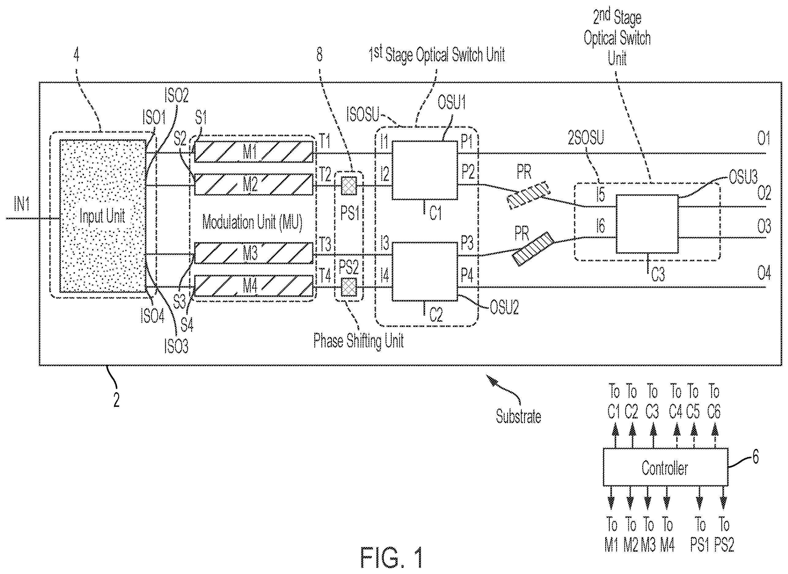
is a schematic of an example PIC chip in accordance with the principles of the present disclosure comprising a reconfigurable unit cell that includes, optically coupled to each other from left to right in the figure, an input unit, a modulation unit (MU), an optional phase shifting unit, a first stage optical switch unit (1SOSU), an optional polarization rotator (PR), and a second stage optical switch unit (2SOSU), wherein the PIC chip may include an optional controller or the controller may be provided separate from the PIC chip;
A- 2 C are schematics of example single, isolated optical switch units of in accordance with the principles of the present disclosure that may be used for each optical switch unit of the first and second stage optical switch units (1SOSU and 2SOSU) in , wherein the single optical switch unit may be set in a bar mode, a cross mode, and a coupler (or 3 db coupler) mode, respectively;
is a schematic of 1×4 splitter in accordance with the principles of the present disclosure that may be used as the input unit of the PIC chip shown in ;
is a schematic of 1:4/2:4 splitter in accordance with the principles of the present disclosure that may be used as the input unit of the PIC chip shown in , wherein the 1:4/2:4 splitter may be formed by one 1×2 splitter cascaded by two 2:2 splitters; and
is a schematic of a number of optical switch units that are optically coupled together in accordance with the principles of the present disclosure that may be used as the input unit of the PIC chip shown in .
DESCRIPTION
Various non-limiting examples will now be described with reference to the accompanying figures where like reference numbers correspond to like or functionally equivalent elements.
For purposes of the description hereinafter, terms like “end,” “upper,” “lower,” “right.” “left.” “vertical,” “horizontal,” “top.” “bottom,” “lateral.” “longitudinal,” and derivatives thereof shall relate to the example(s) as oriented in the drawing figures. However, it is to be understood that the example(s) may assume various alternative variations and step sequences, except where expressly specified to the contrary. It is also to be understood that the specific example(s) illustrated in the attached drawings, and described in the following specification, are simply exemplary examples or aspects of the disclosure. Hence, the specific examples or aspects disclosed herein are not to be construed as limiting.
With reference to , one non-limiting embodiment or example photonics integrated circuit (PIC) chip, in accordance with the principles of this disclosure, comprises a substrate 2 including formed thereon a unit cell comprising an input unit 4 is formed on the substrate 2 . The input unit 4 may include at least one optical input IN 1 and plural optical outputs ISO 1 -ISO 4 . The unit cell may also include a modulation unit (MU) formed on the substrate 2 that includes modulators M 1 -M 4 having optical inputs S 1 -S 4 and optical outputs T 1 -T 4 . The optical inputs S 1 -S 4 are optically coupled to the optical outputs ISO 1 -ISO 4 of the input unit 4 . Each modulator M is operative for modulating light received at the optical input S of the modulator M, in either a phase modulation mode (for coherent applications) or in an amplitude modulation mode (for datacenter applications), by applying, from a controller 6 , a corresponding control signal to the modulator M and for outputting the modulated light on the optical output T of the modulator M. Herein, terms such as “output” and “optical output”; “input” and “optical input”; and “output” and “optical output” may be used interchangeably.
The unit cell may also include a first stage optical switch unit (1SOSU) formed on the substrate 2 . In one non-limiting embodiment or example, the 1SOSU may include a first optical switch unit (OSU 1 ) including optical inputs I 1 and I 2 and optical outputs P 1 and P 2 . In an example, the optical output P 1 may also be considered an optical output O 1 of the PIC chip and, therefore, may be referred to herein interchangeable as optical output P 1 /O 1 or optical output P 1 . In an example, the optical inputs I 1 and I 2 are optically coupled to the optical outputs T 1 and T 2 of the modulators M 1 and M 2 .
The 1SOSU may also include a second optical switch unit (OSU 2 ) including optical inputs I 3 and I 4 and optical outputs P 3 and P 4 . In an example, the optical output P 4 may also be considered an optical output O 4 of the PIC chip and, therefore, may be referred to herein interchangeable as optical output P 4 /O 4 or optical output P 4 . In an example, the optical inputs I 3 and I 4 may be optically coupled to the optical outputs T 3 and T 4 of the modulators M 3 and M 4 .
The unit cell may also include a second stage optical switch unit (2SOSU) formed on the substrate 2 . The 2SOSU may include a third optical switch unit (OSU 3 ) including optical inputs I 5 and I 6 and optical outputs O 2 and O 3 of the PIC chip. In an example, the optical inputs I 5 and I 6 may be optically coupled to optical outputs P 2 and P 3 of OSU 1 and OSU 2 .
In general use of the above-described unit cell, one or more optical (e.g., laser or light) signals input into the at least one optical input IN 1 of input unit 4 is output, at least in-part, by one or more of the outputs ISO 1 -ISO 4 of input unit 4 to one or more of the optical inputs S 1 -S 4 of the modulators M 1 -M 4 of the MU. Each modulator M of the MU receiving an optical signal from the input unit 4 may be operative, in an example, under the control of the controller 6 for modulating the optical signal received at the optical input S of the modulator M and for outputting the modulated optical signal on the optical output T of the modulator M. The controller 6 may be separate from the substrate 2 (as illustrated in ) or may, as may be deemed suitable and/or desirable, be incorporated on the substrate 2 . Herein, the terms “optical signal”, “laser”, “light”, plurals thereof and like terms may be used interchangeably.
The 1SOSU may receive at one or more optical inputs I 1 -I 4 of the OSU 1 and the OSU 2 the modulated optical signals output on one or more of the optical outputs T 1 -T 4 of the modulators M 1 -M 4 . Each of OSU 1 and OSU 2 may route and/or combine (in a manner discussed in greater detail hereinafter) the modulated optical signals output on one or more of the optical outputs T 1 -T 2 and T 3 -T 4 of the modulators M 1 -M 4 and may output the routed and/or combined modulated optical signal on one or more of the optical outputs P 1 -P 4 of OSU 1 and OSU 2 .
As discussed above, the one or more modulated optical signals output on optical outputs P 1 and P 4 of OSU 1 and OSU 2 may be output directly on respective optical outputs O 1 and O 4 of the PIC chip shown in . One or more modulated optical signals output on optical outputs P 2 and P 3 of OSU 1 and OSU 2 may be received at optical inputs I 5 and I 6 of OSU 3 which may route and/or combine the one or more modulated optical signals received at the optical inputs I 5 and I 6 , and which may output the routed and/or combined one or more modulated optical signals received at the optical inputs I 5 and I 6 to outputs O 2 and O 3 of the PIC chip.
In one non-limiting embodiment or example in accordance with the principles of this disclosure, the PIC chip may also comprise a phase shifting unit 8 formed on the substrate including a first phase shifter (PS 1 ) optically coupled between one of the optical inputs I 1 or I 2 of OSU and a corresponding optical output T 1 or T 2 of the modulator M 1 or M 2 . The phase shifting unit 8 may also include a second phase shifter (PS 2 ) optically coupled between one of the optical inputs I 3 or I 4 of OSU 2 and a corresponding optical output T 3 or T 4 of the modulator M 3 or M 4 . The phase shifter operation of each of PS 1 and PS 2 may individually controllable under the control of the controller 6 .
In an example, the first phase shifter (PS 1 ) may be formed on the substrate and be optically coupled between the optical output T 2 of modulator M 2 and the optical input I 2 of OSU 1 and the second phase shifter (PS 2 ) may be formed on the substrate and optically coupled between the optical output T 4 of modulator M 4 and the optical input I 4 of OSU 2 . However, this is not to be construed in a limiting sense since it is envisioned that PS 1 may be optically coupled between the optical output T 1 of modulator M and the optical input I 1 of OSU 1 and/or PS 2 may be optically coupled between the optical output T 3 of modulator M 3 and the optical input I 3 of OSU 2 .
In one non-limiting embodiment or example in accordance with the principles of this disclosure, the PIC chip may also comprise a single polarization rotator (PR) optically coupled between one of the optical outputs P 2 or P 3 of OSU 1 or OSU 2 and one of the optical inputs I 5 or I 6 of OSU 3 . In , the PR is shown (in solid lines) coupled between optical output P 3 of OSU 2 and optical input I 6 of OSU 3 . However, this is not to be construed in a limiting sense since it is envisioned that the PR may instead be coupled (as shown in phantom lines) between optical output P 2 of OSU 1 and optical input I 5 of OSU 3 .
In operation, each phase shifter PS 1 and PS 2 is operative, under the control of the controller 6 , for shifting the phase of the optical signal passing therethrough. In operation, the PR is a passive device that rotates the polarization of an optical signal passing therethrough. The operation of each phase shifter PS and the polarization rotator PR is known in the art and will not be described further herein for the purpose of simplicity.
With reference to A- 2 C and with continuing reference to , in some non-limiting embodiments or examples, each of OSU 1 , OSU 2 , and OSU 3 may be configurable, in a manner known in the art, by controller 6 via the control inputs C 1 , C 2 , and C 3 of OSU 1 , OSU 2 , and OSU 3 , in the following modes as shown, for example, by the isolated views of OSU 1 in A- 2 C :
•
• 1. a bar mode ( A ) wherein optical inputs I 1 and I 2 are optically coupled or routed to optical outputs P 1 and P 2 , respectively; • 2. a cross mode ( B ) wherein optical inputs I 1 and I 2 are optically coupled or routed to optical outputs P 2 and P 1 , respectively; or • 3. a coupler (or 3 dB coupler) mode ( C ) wherein optical signals input on optical inputs I 1 and I 2 are combined by OSU 1 and said combined optical signals is output on both of optical outputs P 1 and P 2 of OSU 1 .
Similarly, as described in greater detail hereinafter in connection with , each of OSU 4 , OSU 5 and OSU 6 of input unit 4 may be configurable in the bar mode, the cross mode, and the coupler mode.
In the isolated views of OSU 1 in A- 2 C , the control input C 1 , shown in , is omitted for simplicity. However, it is to be understood that the control input C 1 is present and utilized by controller 6 to control the mode or state of OSU 1 .
In an example, OSU 1 , OSU 2 , and OSU 3 may be configurable, as a group, (under the control of the controller 6 via control inputs C 1 , C 2 , and C 3 of OSU 1 , OSU 2 , and OSU 3 ) in each of the following modes, one mode at a time:
•
• 1. the bar mode ( A ) wherein optical inputs I 1 , I 2 , I 3 , and I 4 of OSU 1 and OSU 2 are optically coupled to optical outputs P 1 /O 1 , P 2 , P 3 , and P 4 /O 4 of OSU 1 and OSU 2 , and optical inputs I 5 and I 6 of OSU 3 are optically coupled to optical outputs O 2 and O 3 of OSU 3 ; • 2. the cross mode ( B ) wherein optical inputs I 1 , I 2 , I 3 , and I 4 of OSU 1 and OSU 2 are optically coupled to optical outputs P 2 , P 1 /O 1 , P 4 /O 4 , and P 3 of OSU 1 and OSU 2 , and optical inputs I 5 and I 6 of OSU 3 are optically coupled to optical outputs O 3 and O 2 of OSU 3 ; and • 3. the coupler mode ( C ) including: optical input I 1 of OSU 1 optically coupled to optical outputs P 1 /O 1 and P 2 , optical input I 2 of OSU 1 optically coupled to optical outputs P 1 /O 1 and P 2 , optical input I 3 of OSU 2 optically coupled to optical outputs P 3 and P 4 /O 4 , optical input I 4 of OSU 2 optically coupled to optical outputs P 3 and P 4 /O 4 , optical input I 5 of OSU 3 optically coupled to optical outputs O 2 and O 3 , and optical input I 6 of OSU 3 optically coupled to optical outputs O 2 and O 3 , wherein, light input into each optical input is split between the corresponding optical outputs.
With reference to and with continuing reference to all previous figures, in some non-limiting embodiments or examples in accordance with the principles of this disclosure, the input unit may comprise one of the following:
•
• 1. a 1:4 splitter ( ) including the at least one optical input IN 1 optically coupled to the optical outputs ISO 1 -ISO 4 ; or • 2. a 1:4/2:4 splitter, formed, in an example, by one 1:2 splitter cascaded by two 2:2 splitters, ( ) including: (a) an optical input IN 2 optically coupled to the optical outputs ISO 1 -ISO 4 , or (b) the optical input IN 1 optically coupled to the optical outputs ISO 1 and ISO 2 and (c) an optical input IN 4 optically coupled to the optical outputs ISO 3 and ISO 4 ; or • 3. a combination ( ) including: a fourth optical switch unit (OSU 4 ) including optical inputs IN 2 and IN 3 and optical outputs IO 2 and IO 3 , a fifth optical switch unit (OSU 5 ) including the optical input IN 1 and an optical input IN 5 coupled to the optical output IO 2 of OSU 4 and the optical outputs ISO 1 and ISO 2 , and a sixth optical switch unit (OSU 6 ) including an optical input IN 4 , an optical input IN 6 coupled to the optical output IO 3 of OSU 4 , and the optical outputs ISO 3 and ISO 4 .
With continuing reference to and reference back to A- 2 C , in some non-limiting embodiments or examples, each of OSU 4 , OSU 5 , and OSU 6 (like OSU 1 , OSU 2 , and OSU 3 described above) may be configurable, by controller 6 via the control inputs C 4 , C 5 , and C 6 of OSU 4 , OSU 5 , and OSU 6 , in the bar mode, the cross mode, or the coupler (or 3 dB coupler) mode as shown, for example, by the isolated view of OSU 1 in A- 2 C .
With continuing reference to , the OSU 4 , OSU 5 , and OSU 6 of the input unit may be configurable, as a group, (under the control of the controller 6 via control inputs C 4 , C 5 , and C 6 of OSU 4 , OSU 5 , and OSU 6 ) in the following modes, one-mode at a time:
•
• 1. the bar mode including the optical inputs IN 1 -IN 4 optically coupled to the optical outputs ISO 1 -ISO 4 ; or • 2. the cross mode including the optical inputs IN 1 , IN 2 , IN 3 , and IN 4 optically coupled to the optical outputs ISO 2 , ISO 4 , ISO 1 , and ISO 3 ; or • 3. the coupler mode including: the optical input IN 1 optically coupled to the optical outputs ISO 1 and ISO 2 , the optical input IN 2 optically coupled to the optical outputs ISO 1 -ISO 4 , the optical input IN 3 optically coupled to the optical outputs ISO 1 -ISO 4 , the optical input IN 4 optically coupled to the optical outputs ISO 3 and ISO 4 , the optical input IN 5 optically coupled to the optical outputs ISO 1 and ISO 2 , and the optical input IN 6 optically coupled to the optical outputs ISO 3 and ISO 4 , wherein, light input into each optical input is split between the corresponding optical outputs.
In some non-limiting embodiments or examples, when OSU 4 -OSU 6 of the input unit 4 are in the coupler mode, light input into the optical inputs IN 1 -IN 4 is split evenly between the optical outputs ISO 1 -ISO 4 .
Various configurations of OSU 4 , OSU 5 , and/or OSU 6 of the input unit 4 will now be described with reference to A- 2 C and 5 .
OSU 4 in Bar Mode and OSU 5 in Coupler Mode
In one non-limiting embodiment or example, when OSU 4 is configured in a bar mode, wherein optical inputs IN 2 and IN 3 are optically coupled to the optical outputs IO 2 and IO 3 , and OSU 5 is configured in a coupler mode, wherein the optical input IN 1 is optically coupled to the optical outputs ISO 1 and ISO 2 and the optical input IN 5 , which is optically coupled to the optical output IO 2 of OSU 4 , is optically coupled to the optical outputs ISO 1 and ISO 2 , the optical signal output on each of the optical inputs ISO 1 and ISO 2 may be the combination of the optical signals input into the optical inputs IN 1 and IN 2 .
OSU 4 in Bar Mode and OSU 6 in Coupler Mode
In another non-limiting embodiment or example, when OSU 4 is configured in a bar mode, wherein optical inputs IN 2 and IN 3 are optically coupled to the optical outputs IO 2 and IO 3 , and OSU 6 is configured in a coupler mode, wherein the optical input IN 4 is optically coupled to the optical outputs ISO 3 and ISO 4 and the optical input IN 5 , which is optically coupled to the optical output IO 3 of OSU 4 , is optically coupled to the optical outputs ISO 3 and ISO 4 , the optical signal output on each of the optical inputs ISO 3 and ISO 4 may be the combination of optical signals input into the optical inputs IN 3 and IN 4 .
OSU 4 in Cross Mode and OSU 5 in Coupler Mode
In another non-limiting embodiment or example, when OSU 4 is configured in a cross mode, wherein the optical inputs IN 2 and IN 3 are optically coupled to the optical outputs IO 3 and IO 2 , and OSU 5 is configured in a coupler mode, wherein the optical input IN 1 is optically coupled to the optical outputs ISO 1 and ISO 2 , and the optical input IN 5 , which is optically coupled to the optical output IO 2 of OSU 4 , is optically coupled to the optical outputs ISO 1 and ISO 2 , the optical signal output on each of the optical outputs ISO 1 and ISO 2 is a combination of optical signals input into the optical inputs IN 1 and IN 3 .
OSU 4 in Cross Mode and OSU 6 in Coupler Mode
In another non-limiting embodiment or example, when OSU 4 is configured in a cross mode, wherein the optical inputs IN 2 and IN 3 are optically coupled to the optical outputs IO 3 and IO 2 , and OSU 6 is configured in a coupler mode, wherein the optical input IN 4 is optically coupled to the optical outputs ISO 3 and ISO 4 , and the optical input IN 5 , which is optically coupled to the optical output IO 3 of OSU 4 , is optically coupled to the optical outputs ISO 3 and ISO 4 , the optical signal output on each of the optical outputs ISO 3 and ISO 4 is a combination of optical signals input into the optical inputs IN 2 and IN 4 .
OSU 4 in Bar Mode and OSU 5 in Bar Mode
In another non-limiting embodiment or example, when OSU 4 is configured in a bar mode, wherein the optical inputs IN 2 and IN 3 are optically coupled to the optical outputs IO 2 and IO 3 , and OSU 5 is configured in a bar mode wherein the optical input IN 1 is optically coupled to the optical output ISO 1 and the optical input IN 5 , which is optically coupled to the optical output IO 2 of OSU 4 , is optically coupled to the optical output ISO 2 , the optical signals output on the optical outputs ISO 1 and ISO 2 are the optical signals input into the optical inputs IN 1 and IN 2 .
OSU 4 in Bar Mode and OSU 6 in Bar Mode
In another non-limiting embodiment or example, when OSU 4 is configured in a bar mode, wherein the optical inputs IN 2 and IN 3 are optically coupled to the optical outputs IO 2 and IO 3 , and OSU 6 is configured in a bar mode wherein the optical input IN 4 is optically coupled to the optical output ISO 4 and the optical input IN 3 , which is optically coupled to the optical output IO 3 of OSU 4 , is optically coupled to the optical output ISO 3 , whereupon the optical signals output on the optical outputs ISO 3 and ISO 4 are the optical signals input into the optical inputs IN 3 and IN 4 .
OSU 4 in Bar Mode and OSU 5 in Cross Mode
In another non-limiting embodiment or example, when OSU 4 is configured in a bar mode, wherein the optical inputs IN 2 and IN 3 are optically coupled to the optical outputs IO 2 and IO 3 , and OSU 5 is configured in a cross mode, wherein the optical input IN 1 is optically coupled to the optical output ISO 2 and the optical input IN 5 , which is optically coupled to the optical output IO 2 of OSU 4 , is optically coupled to the optical output ISO 1 , the optical signals output on the optical outputs ISO 1 and ISO 2 are the optical signals input into the optical inputs IN 2 and IN 1 .
OSU 4 in Bar Mode and OSU 6 in Cross Mode
In another non-limiting embodiment or example, when OSU 4 is configured in a bar mode, wherein the optical inputs IN 2 and IN 3 are optically coupled to the optical outputs IO 2 and IO 3 , and OSU 6 is configured in a cross mode, wherein the optical input IN 4 is optically coupled to the optical output ISO 3 and the optical input IN 6 , which is optically coupled to the optical output IO 3 of OSU 4 , is optically coupled to the optical output ISO 4 , the optical signals output on the optical outputs ISO 3 and ISO 4 are the optical signals input into the optical inputs IN 4 and IN 3 .
OSU 4 in Cross Mode and OSU 5 in Bar Mode
In another non-limiting embodiment or example, when OSU 4 is configured in a cross mode, wherein the optical inputs IN 2 and IN 3 are optically coupled to the optical outputs IO 3 and IO 2 , and OSU 5 is configured in a bar mode, wherein the optical input IN 1 is optically coupled to the optical output ISO 1 and the optical input IN 5 , which is optically coupled to the optical output IO 2 of OSU 4 , is optically coupled to the optical output ISO 2 , the optical signals output on the optical outputs ISO 1 and ISO 2 are the optical signals input into the optical inputs IN 1 and IN 3 .
OSU 4 in Cross Mode and OSU 6 in Bar Mode
In another non-limiting embodiment or example, when OSU 4 is configured in a cross mode, wherein the optical inputs IN 2 and IN 3 are optically coupled to the optical outputs IO 3 and IO 2 , and OSU 6 is configured in a bar mode, wherein the optical input IN 4 is optically coupled to the optical output ISO 4 and the optical input IN 6 , which is optically coupled to the optical output IO 3 of OSU 4 , is optically coupled to the optical output ISO 3 , the optical signals output on the optical outputs ISO 3 and ISO 4 are the optical signals input into the optical inputs IN 2 and IN 4 .
OSU 4 in Cross Mode and OSU 5 in Cross Mode
In another non-limiting embodiment or example, when OSU 4 is configured in a cross mode, wherein the optical inputs IN 2 and IN 3 are optically coupled to the optical outputs IO 3 and IO 2 , and OSU 5 is configured in a cross mode, wherein the optical input IN 1 is optically coupled to the optical output ISO 2 and the optical input IN 5 , which is optically coupled to the optical output IO 2 of OSU 4 , is optically coupled to the optical output ISO 1 , the optical signals output on the optical outputs ISO 1 and ISO 2 are the optical signals input into the optical inputs IN 3 and IN 1 .
OSU 4 in Cross Mode and OSU 6 in Cross Mode
In another non-limiting embodiment or example, when OSU 4 is configured in a cross mode, wherein the optical inputs IN 2 and IN 3 are optically coupled to the optical outputs IO 3 and IO 2 , and OSU 6 is configured in a cross mode, wherein the optical input IN 4 is optically coupled to the optical output ISO 3 and the optical input IN 6 , which is optically coupled to the optical output IO 3 of OSU 4 , is optically coupled to the optical output ISO 4 , the optical signals output on the optical outputs ISO 3 and ISO 4 are the optical signals input into the optical inputs IN 4 and IN 2 .
With continuing reference to all of the figures, also disclosed herein, in one non-limiting embodiment or example in accordance with the principles of this disclosure, is a photonics integrated circuit (PIC) chip comprising a substrate 2 including a unit cell comprising an input unit 4 formed on the substrate and having at least one optical input (IN) and a plurality of optical outputs (ISO). A modulation unit (MU) of the a unit cell may also be formed on the substrate and include a plurality of modulators (M) having optical inputs(S) and optical outputs (T). The plurality of optical inputs S of the MU may be optically coupled to the plurality of optical outputs ISO of the input unit. Each modulator M may be operative for modulating light received at the optical input S of the modulator M and for outputting the modulated light on the optical output T of the modulator M.
A first stage optical switch unit (1SOSU) of the a unit cell may be formed on the substrate and may include a plurality of optical inputs (I) and first and second subsets of optical outputs (P). The plurality of optical inputs I of the 1SOSU may be optically coupled to the plurality of optical outputs T of the MU. The first subset of the optical outputs P (e.g., P 1 and P 4 ) of the 1SOSU may define a first subset of optical outputs O (e.g., O 1 and O 4 ) of the PIC chip.
A second stage optical switch unit (2SOSU) of the a unit cell may be formed on the substrate and may include a plurality of optical inputs I and a second subset of the optical outputs O (O 2 and O 3 ) of the PIC chip, wherein the plurality of optical inputs I (e.g., I 5 and I 6 ) of the 2SOSU may be optically coupled to the second subset of the optical outputs P (e.g., P 2 and P 3 ) of the 1SOSU.
The 1SOSU and the 2SOSU may be configured by the controller 6 in the following modes:
•
• 1. a coupler mode, wherein at least portions of the optical outputs T of the plurality of modulators M may be combined at each optical output O (e.g., O 1 -O 4 ) of the 1SOSU and the 2SOSU; • 2. a bar mode, wherein a first subset of the optical outputs T (e.g., T 1 and T 4 ) of the plurality of modulators M may be output directly on the first subset of the optical outputs O (e.g., O 1 and O 4 ) of the PIC chip and a second subset of the optical outputs T (e.g., T 2 and T 3 ) of the plurality of modulators M may be output on the second subset of the optical outputs O (e.g., O 2 and O 3 ) of the PIC chip via the 2SOSU; and • 3. a cross mode, wherein a first subset of the optical outputs T (e.g., T 2 and T 3 ) of the plurality of modulators M may be crossed by the 1SOSU and output on the first subset of the optical outputs O (e.g., O 1 and O 4 ) of the PIC chip and a second subset of the optical outputs T (T 1 and T 4 ) of the plurality of modulators M may be crossed by the 2SOSU and is output on the second subset of the optical outputs O (e.g., O 2 and O 3 ) of the PIC chip.
Hereinafter, the variable “x” may be any whole number. Accordingly, the indication herein of any specific value of “x” for the purpose of example is not to be construed in a limiting sense.
In an example in accordance with the principles of this disclosure, the 1SOSU may include optical inputs I 1 -Ix (e.g., I 1 -I 4 ) and may include optical outputs P 1 -Px (e.g., P 1 -P 4 ) which define at least some optical outputs O 1 -Ox (e.g., O 1 and O 4 ) of the PIC chip.
In an example in accordance with the principles of this disclosure, the 2SOSU may include optical inputs I 1 ′-Ix′ (e.g., I 5 and I 6 ) and may include optical outputs O 1 ′-Ox′ (e.g., O 2 and O 3 ) of the PIC chip.
In an example in accordance with the principles of this disclosure, when the 1SOSU is in the bar mode, the optical inputs I 1 -Ix (e.g., I 1 -I 4 ) of the 1SOSU may be coupled to the respective optical outputs P 1 -Px (e.g., P 1 -P 4 ) of the 1SOSU.
In an example in accordance with the principles of this disclosure, when the 2SOSU is in the bar mode, the optical inputs I 1 ′-Ix′ (e.g., I 5 and I 6 ) of the 2SOSU may be coupled to the respective optical outputs O 1 ′-Ox′ (e.g., O 2 and O 3 ) of the PIC chip.
In an example in accordance with the principles of this disclosure, when the 1SOSU is in the coupler mode, at least portions of the optical inputs I 1 -Ix (e.g., I 1 -I 2 and I 3 -I 4 ) of the 1SOSU may be combined at each of the optical outputs P 1 -Px (e.g., P 1 -P 2 and P 3 -P 4 ) of the 1SOSU.
In an example in accordance with the principles of this disclosure, when the 2SOSU is in the coupler mode, at least portions of the optical inputs I 1 ′-Ix′ (e.g., I 5 -I 6 ) of the 2SOSU may be combined at each of the optical outputs O 1 ′-Ox′ (e.g., O 2 -O 3 ) of the PIC chip.
In an example in accordance with the principles of this disclosure, when the 1SOSU is in the cross mode, the optical inputs I 1 -Ix (e.g., I 1 -I 2 and I 3 -I 4 ) of the 1SOSU may be coupled to the respective optical outputs Px-P 1 (e.g., P 2 -P 1 and P 4 -P 3 ) of the 1SOSU.
Finally, in an example in accordance with the principles of this disclosure, when the 2SOSU is in the cross mode, the optical inputs I 1 ′-Ix′ (e.g., I 5 -I 6 ) of the 2SOSU may be coupled to the respective optical outputs Ox′-O 1 ′ (e.g., O 3 -O 2 ) of the PIC chip.
In some non-limiting embodiments or examples in accordance with the principles of this disclosure, an optional phase shifting unit of the a unit cell may be formed on the substrate 2 between the MU and the 1SOSU. In an example, the phase shifting unit may include a first phase shifter (PS 1 ) formed on the substrate and optically coupled between one of the optical inputs I 1 or I 2 of OSU 1 and a corresponding optical output T 1 or T 2 of the modulator M 1 or M 2 . The phase shifting unit may also include a second phase shifter (PS 2 ) formed on the substrate and optically coupled between one of the optical inputs I 3 or I 4 of OSU 2 and a corresponding optical output T 3 or T 4 of the modulator M 3 or M 4 . In a specific example, the first phase shifter (PS 1 ) may be optically coupled between the optical output T (e.g., T 2 ) of a first of the plurality of modulators M (e.g., M 2 ) and a first of the plurality of optical inputs I (e.g., I 2 ) of the 1SOSU. The phase shifting unit may also include a second phase shifter (PS 2 ) optically coupled between the optical output T (e.g., T 4 ) of a second of the plurality of modulators M (e.g., M 4 ) and a second of the plurality of optical inputs I (e.g., I 4 ) of the 1SOSU. In some non-limiting embodiments or examples in accordance with the principles of this disclosure, an optional polarization rotator of the a unit cell may be formed on the substrate 2 between one of the optical outputs P (e.g., P 2 or P 3 )) the 1SOSU and one of the optical inputs I′ (e.g., I 5 or I 6 ) of the 2SOSU.
In an example in accordance with the principles of this disclosure, the input unit may comprise at least one of the following: a 1:4 splitter or a 2:4 splitter.
In an example in accordance with the principles of this disclosure, the input unit may comprise an input optical switch unit including a plurality of optical inputs (IN 1 -INx) (e.g., IN 1 -IN 4 ) and the plurality of optical outputs (ISO 1 -ISOx) (e.g., ISO 1 -ISO 4 ), wherein the input optical switch unit may be configurable by the controller 6 in the following modes:
•
• 1. a coupler mode, wherein at least portions of optical signals input into the plurality of optical inputs IN 1 -INx (e.g., IN 1 -IN 4 ) of the input optical switch unit are combined at each optical output ISO 1 -ISOx (e.g., ISO 1 -ISO 4 ) of the input optical switch unit; • 2. a bar-bar mode, wherein optical signals input into the plurality of optical inputs IN 1 -INx (e.g., IN 1 -IN 4 ) of the input optical switch unit are output directly to the respective optical outputs ISO 1 -ISOx (e.g., ISO 1 -ISO 4 ) of the input optical switch unit; • 3. a bar-coupler or cross-coupler mode, wherein a subset of at least portions of the optical signals input into the plurality of optical inputs IN 1 -INx (e.g., IN 1 -IN 4 ) of the input optical switch unit are combined and output on a subset optical output ISO 1 -ISOx (e.g., ISO 1 -ISO 4 ) of the input optical switch unit; and • 4. bar-cross or a cross-cross mode, wherein a subset of the optical signals input into the plurality of optical inputs IN 1 -INx (e.g., IN 1 -IN 4 ) of the input optical switch unit are crossed and output to optical outputs ISOx-ISO 1 (e.g., ISO 4 -ISO 1 ) of the input optical switch unit.
As can be understood from the foregoing, by selection of an appropriate one of the input units 4 shown in to use with the combination of the MU, the phase shifting unit 8 , the 1SOSU, the PR, and the 2SOSU shown in , the PIC chip can be configured to support various datacenter IMDD and/or telecom coherent transmission applications.
Herein, the input unit 4 is illustrated and described as being formed on the same substrate 2 as the MU, the phase shifting unit 8 , the 1SOSU, the PR, and the 2SOSU. However, this is not to be construed in a limiting sense since it is envisioned the input unit 4 may be formed on a separate substrate (not shown) and optically coupled, in a manner known in the art, to the substrate 2 that includes the MU, the phase shifting unit 8 , the 1SOSU, the PR, and the 2SOSU—but excludes the input unit 4 . In this way, the different input units 4 shown in can be selectively used with the substrate 2 that includes the MU, the phase shifting unit 8 , the 1SOSU, the PR, and the 2SOSU (but excludes the input unit 4 ). Furthermore, each input unit 4 shown in can be manufactured as first photonics chip, as needed, separately from a second photonics chip that includes the substrate 2 including the MU, the phase shifting unit 8 , the 1SOSU, the PR, and the 2SOSU (but excluding the input unit 4 ), whereupon the second photonics chip can be utilized, as needed, with a first photonics chip that includes appropriate circuitry, e.g., the 1×4 splitter ( ), or the 1:4/2:4 splitter ( ), or the OSU 4 -OSU 6 ( ), deemed suitable and/or desirable for a particular application, e.g., datacenter IMDD and/or telecom coherent transmission.
Finally, the controller 6 may be formed on or off of the substrate 2 as may be deemed suitable and/or desirable for a particular application.
Although the disclosure has been described in detail for the purpose of illustration based on what is currently considered to be the most practical and preferred embodiments, it is to be understood that such detail is solely for that purpose and that the disclosure is not limited to the disclosed embodiments, but, on the contrary, is intended to cover modifications and equivalent arrangements that are within the spirit and scope of the appended claims. For example, it is to be understood that the present disclosure contemplates that, to the extent possible, one or more features of any embodiment can be combined with one or more features of any other embodiment.
Figures (3)
Citations
This patent cites (7)
- US9547214
- US10175422
- US2013/0209020
- US2019/0391243
- US2020/0256728
- US2023/0027271
- US2148456