Power Supply Device, and Control Method for Power Supply Device
Abstract
A power supply device of the present invention includes a storage circuit including electrical double layer capacitor between first node connected to a power supply, which is an in-vehicle battery, and second node grounded; a charge circuit connected to the first node and configured to charge the storage circuit; and a power supply controller configured to measure voltage at the first node and control the charge circuit. The power supply controller performs procedure of causing the charge circuit to charge the storage circuit and computing first capacitance value and first equivalent series resistance value of the electrical double layer capacitor based on voltage measured at the first node, upon determining the voltage at the first node is lower than a threshold voltage value, that is, determining a stop period of a vehicle is longer than a threshold period.
Claims (5)
1 . A power supply device, comprising: a storage circuit including a first node connected to a power supply, a second node that is grounded, and an electrical double layer capacitor between the first node and the second node; a charge circuit connected to the first node and configured to charge the storage circuit; a power supply controller configured to measure a voltage at the first node and control the charge circuit, wherein the power supply controller is configured to perform, when a stop period of an engine is longer than a threshold period, a procedure of causing the charge circuit to charge the storage circuit and computing a first capacitance value and a first equivalent series resistance value based on the voltage measured at the first node; and a discharge circuit connected to the first node and configured to discharge the storage circuit, wherein the power supply controller is configured to perform, when the stop period of the engine is shorter than or equal to the threshold period, a procedure of computing a second capacitance value and a second equivalent series resistance value of the electrical double layer capacitor based on the voltage at the first node while discharging the storage circuit by the discharge circuit.
4 . A power supply device, comprising: a storage circuit including a first node connected to a power supply, a second node that is grounded, a third node between the first node and the second node, and an electrical double layer capacitor between the first node and the second node; a charge circuit connected to the first node and configured to charge the storage circuit; and a power supply controller configured to measure a voltage at the first node and a voltage at the third node, and control the charge circuit, wherein the power supply controller performs a procedure of causing the charge circuit to charge the storage circuit and computing a first capacitance value and a first equivalent series resistance value based on the voltage measured at the first node and the voltage measured at the third node, in response to determining that a stop period is longer than a threshold period.
5 . A control method for a power supply device including a storage circuit including a first node connected to a power supply, a second node that is grounded, and an electrical double layer capacitor between the first node and the second node; a charge circuit connected to the first node and configured to charge the storage circuit; and a discharge circuit connected to the first node and configured to discharge the storage circuit, the control method comprising: performing, when a stop period of an engine is longer than a threshold period, a procedure of causing the charge circuit to charge the storage circuit and computing a first capacitance value and a first equivalent series resistance value based on a voltage measured at the first node; and performing, when the stop period of the engine is shorter than or equal to the threshold period, a procedure of computing a second capacitance value and a second equivalent series resistance value of the electrical double layer capacitor based on the voltage at the first node while discharging the storage circuit by the discharge circuit.
Show 2 dependent claims
2 . The power supply device according to claim 1 , wherein the power supply controller is configured to estimate the stop period based on the voltage at the first node.
3 . The power supply device according to claim 1 , wherein the power supply controller determines degradation of the electrical double layer capacitor based on the second capacitance value and the second equivalent series resistance value, in response to determining that the stop period is shorter than the threshold period.
Full Description
Show full text →
TECHNICAL FIELD
The present disclosure relates to power supply devices, and control methods for power supply devices.
BACKGROUND ART
In a vehicle, a known backup power supply is provided to supply electric energy in place of a main power supply or to supplement the main power supply, in a case where a failure or interruption of the main power supply occurs (see, for example, Patent Document 1).
PRIOR ART DOCUMENTS
Patent Documents
• Patent Document 1: Japanese Patent No. 6675874
DISCLOSURE OF THE INVENTION
Problem to be Solved by the Invention
Patent Document 1 discloses using a super capacitor as the backup power supply. Patent Document 1 discloses including a diagnostic module configured to monitor a state-of-health of a supercapacitor by measuring capacitance value and internal equivalent resistance.
A capacitance value and an equivalent series resistance value of an electrical double layer capacitor measured upon discharge may be ineffective as characteristics of the electrical double layer capacitor after a long time has passed from the discharge. Meanwhile, when characteristics of an electrical double layer capacitor are measured every time upon start of use, it takes time to start-up a power supply device.
The present disclosure provides a power supply device in which characteristics of an electrical double layer capacitor that are effective upon start of use, can be obtained.
Means of Solving the Problem
According to one aspect of the present disclosure, there is provided a power supply device including: a storage circuit including a first node connected to a power supply, a second node that is grounded, and an electrical double layer capacitor between the first node and the second node; a charge circuit connected to the first node and configured to charge the storage circuit; and a power supply controller configured to measure a voltage at the first node and control the charge circuit. The power supply controller performs a procedure of causing the charge circuit to charge the storage circuit and computing a first capacitance value and a first equivalent series resistance value based on the voltage measured at the first node, in response to determining that a stop period is longer than a threshold period.
Effects of the Invention
According to the power supply device of the present disclosure, it is possible to obtain characteristics of an electrical double layer capacitor that are effective upon start of use.
BRIEF DESCRIPTION OF THE DRAWINGS
is a diagram illustrating a configuration example of a power supply device according to a first embodiment.
is a diagram illustrating a configuration example of an equalization and discharge circuit of the power supply device according to the first embodiment.
is a flowchart illustrating a processing procedure of the power supply device according to the first embodiment.
is a flowchart illustrating the processing procedure of the power supply device according to the first embodiment.
is a flowchart illustrating a discharge-based characteristics measurement process of the power supply device according to the first embodiment.
is an equivalent circuit diagram of a circuit configured to perform the discharge-based characteristics measurement process of a storage circuit in the power supply device according to the first embodiment.
is a flowchart of a capacitance value measurement process of the storage circuit in the power supply device according to the first embodiment.
is a flowchart of an equivalent series resistance value measurement process of the storage circuit in the power supply device according to the first embodiment.
is a flowchart of a capacitance value and equivalent series resistance value measurement process (characteristics measurement process) of the storage circuit in the power supply device according to the first embodiment.
is an equivalent circuit diagram of a circuit configured to perform an equalization process of the storage circuit in the power supply device according to the first embodiment.
is a flowchart of the equalization process of the storage circuit in the power supply device according to the first embodiment.
is a flowchart of a discharge process of the storage circuit in the power supply device according to the first embodiment.
is a flowchart illustrating a charge-based characteristics measurement process of the power supply device according to the first embodiment.
is an equivalent circuit diagram of a circuit configured to perform the charge-based characteristics measurement process of the storage circuit in the power supply device according to the first embodiment.
is a flowchart of the capacitance value measurement process of the storage circuit in the power supply device according to the first embodiment.
is a flowchart of the equivalent series resistance value measurement process of the storage circuit in the power supply device according to the first embodiment.
is a flowchart of a charge process of the storage circuit in the power supply device according to the first embodiment.
is a diagram illustrating a configuration example of a power supply device according to a second embodiment.
is a flowchart illustrating a discharge-based characteristics measurement process of the power supply device according to the second embodiment.
is an equivalent circuit diagram of a circuit configured to perform the discharge-based characteristics measurement process of a storage circuit in the power supply device according to the second embodiment.
is a flowchart of a capacitance value measurement process of the storage circuit in the power supply device according to the second embodiment.
is a flowchart of an equivalent series resistance value measurement process of the storage circuit in the power supply device according to the second embodiment.
is a flowchart of a charge-based characteristics measurement process of the power supply device according to the second embodiment.
is an equivalent circuit diagram of a circuit configured to perform the charge-based characteristics measurement process of the storage circuit in the power supply device according to the second embodiment.
is a flowchart of the capacitance value measurement process of the storage circuit in the power supply device according to the second embodiment.
is a flowchart of the equivalent series resistance value measurement process of the storage circuit in the power supply device according to the second embodiment.
is a flowchart of a characteristics measurement process of a power supply device according to a third embodiment.
MODE OF CARRYING OUT THE INVENTION
Hereinafter, the power supply device according to the present embodiment will be described in detail with reference to the drawings.
First Embodiment
<Power Supply Device 1 >
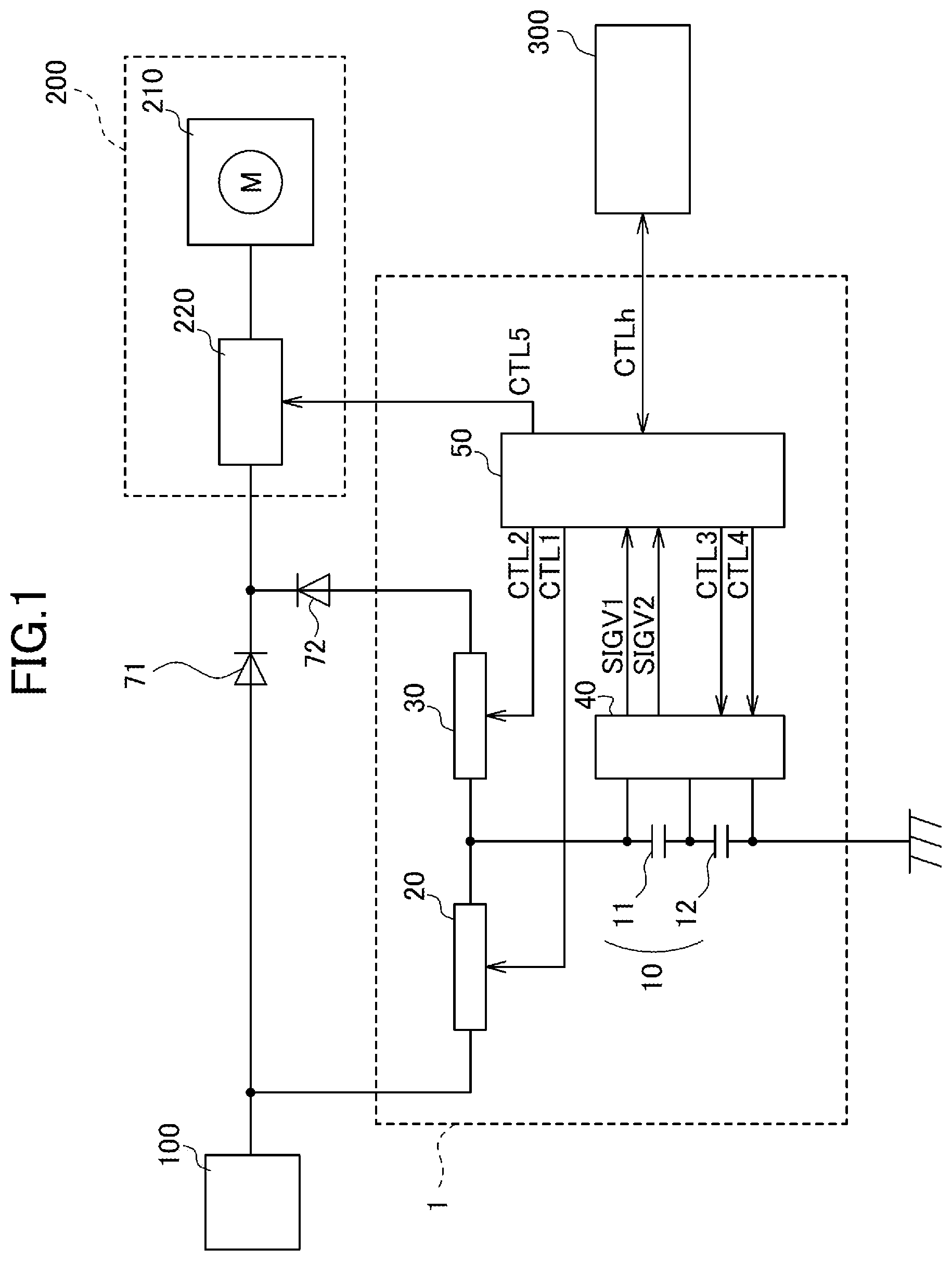
is a diagram illustrating a configuration example of a power supply device 1 according to the present embodiment. In recent years, in a latch mechanism that is a mechanical lock mechanism of an automobile door, a system that operates a lock portion of a latch by a motor is adopted as an electric latch system. The automobile door is required to unlock even in case of an emergency, such as an accident or the like. For this reason, even in a case where a battery power supply fails due to breakage or the like caused by the accident, the electric latch system is required to continue operating for a certain period of time. The power supply device 1 according to the present embodiment is used, for example, as a backup power supply for the electric latch system.
The power supply device 1 stores electric power supplied from a power supply 100 . In addition, the power supply device 1 supplies electric power to a load device 200 when the electric power from the power supply 100 is cut off. The power supply 100 is also directly connected to the load device 200 . The power supply 100 is connected to the load device 200 via a diode 71 , in order to prevent a reverse current.
The power supply 100 is an in-vehicle battery, for example. The load device 200 includes a load 210 , and a load driving circuit 220 configured to drive the load 210 . The load 210 is a motor in an electric latch system of a motor vehicle door, for example.
The power supply device 1 includes a storage circuit 10 , a charge circuit 20 , a boosting circuit 30 , an equalization and discharge circuit 40 , and a power supply controller 50 . Each of these constituent elements of the power supply device 1 will be described.
[Storage Circuit 10 ]
The storage circuit 10 is a circuit configured to store electric power. The storage circuit 10 includes at least one electrical double layer capacitor, that is, a so-called super capacitor. The storage circuit 10 of the power supply device 1 according to the present embodiment includes an electrical double layer capacitor 11 and an electrical double layer capacitor 12 that are connected in series.
[Charge Circuit 20 ]
The charge circuit 20 is configured to charge the storage circuit 10 with the electric power supplied from the power supply 100 . The charge circuit 20 performs a charge process based on a charge control signal CTL 1 of the power supply controller 50 .
[Boosting Circuit 30 ]
The boosting circuit 30 is configured to boost the electric power supplied from the storage circuit 10 , and supply the boosted electric power to the load device 200 . The boosting circuit 30 supplies the electric power based on a boosting control signal CTL 2 of the power supply controller 50 . The boosting circuit 30 is connected to the load device 200 via a diode 72 , in order to prevent a reverse current. The diode 72 may be omitted.
[Equalization and Discharge Circuit 40 ]
The equalization and discharge circuit 40 is configured to perform an equalization process to the storage circuit 10 . In addition, the equalization and discharge circuit 40 performs a discharge process on the storage circuit 10 . is a diagram illustrating a configuration example of the equalization and discharge circuit 40 of the power supply device 1 according to the present embodiment.
In a case where the electrical double layer capacitors, such as the super capacitors or the like, are connected in series, an imbalance may occur in voltage sharing of the capacitors due to variations in individual leakage currents, variations in individual capacitances, or the like. When the imbalance occurs in the voltage sharing of the capacitors, there is a possibility that a voltage exceeding a rated value or a set value will be applied to one of the capacitors, even if a voltage of the series-connected capacitors as a whole, obtained by adding the rated voltages of the individual capacitors, falls within a rated voltage. In order to prevent the voltage exceeding the rated value or the set value from being applied to the electrical double layer capacitor 11 or the electrical double layer capacitor 12 , the equalization and discharge circuit 40 performs the equalization process to eliminate a voltage sharing imbalance and equalize voltages applied to the respective capacitors.
The equalization and discharge circuit 40 performs the equalization process and the discharge process of the storage circuit 10 by a SW 1 control signal CTL 3 for opening and closing a switch 41 and a SW 2 control signal CTL 4 for opening and closing a switch 42 . In addition, the equalization and discharge circuit 40 outputs a voltage signal SIGV 1 of an electrical double layer capacitor 11 and a voltage signal SIGV 2 of an electrical double layer capacitor 12 , to the power supply controller 50 .
The equalization and discharge circuit 40 includes the switches 41 and 42 , and resistors 45 and 46 . The storage circuit 10 includes the electrical double layer capacitor 11 between a node N 1 and a node N 3 . The storage circuit 10 includes the electrical double layer capacitor 12 between the node N 3 and a node N 2 . The node N 1 is connected to the power supply 100 and the load device 200 . The node N 2 is grounded.
The switch 41 includes a first terminal 41 a and a second terminal 41 b . The switch 41 makes a connection or disconnection between the first terminal 41 a and the second terminal 41 b . The switch 41 is provided between the node N 1 and a resistor 45 . In the following description, the switch 41 may also be referred to as a switch SW 1 . The switch 41 is opened and closed based on the SW 1 control signal CTL 3 .
The resistor 45 is provided between the switch 41 and a node N 4 . The resistor 45 and a resistor 46 are connected in series at the node N 4 . The resistor 45 has a resistance value R 1 .
The switch 42 includes a first terminal 42 a and a second terminal 42 b . The switch 42 makes a connection or disconnection between the first terminal 42 a and the second terminal 42 b . The switch 42 is provided between the node N 2 and the resistor 46 . In the following description, the switch 42 may also be referred to as a switch SW 2 . The switch 42 is opened and closed based on the SW 2 control signal CTL 4 .
The resistor 46 is provided between the node N 4 and the node N 2 . The resistor 46 has a resistance value R 2 . The resistance value R 2 may be equal to the resistance value R 1 . A case where the resistance values are equal to each other is not limited to the case where the resistance values perfectly match each other, and includes the case where the resistance values are the same within a range including a manufacturing error, for example.
The equalization and discharge circuit 40 outputs a terminal voltage Vtc 1 at the node N 1 to the power supply controller 50 , as the voltage signal SIGV 1 . Moreover, the equalization and discharge circuit 40 outputs a terminal voltage Vtc 2 at the node N 3 to the power supply controller 50 , as the voltage signal SIGV 2 . The voltage at the node N 1 may also be referred to as a terminal voltage Vtc of the storage circuit 10 .
The node N 1 is an example of the first node, and the node N 2 is an example of the second node.
[Power Supply Controller 50 ]
The power supply controller 50 is configured to control charge, power supply, discharge, and equalization of the storage circuit 10 . Also, the power supply controller 50 measures the characteristics of the storage circuit 10 . The power supply controller 50 is formed by, for example, a controller such as a microcontroller or the like.
The power supply controller 50 controls charge to the storage circuit 10 by the charge circuit 20 , using the charge control signal CTL 1 . Also, the power supply controller 50 controls power supply to the load device 200 of the boosting circuit 30 , using the boosting control signal CTL 2 . The power supply controller 50 controls the equalization process of the equalization and discharge circuit 40 , using the SW 1 control signal CTL 3 or the SW 2 control signal CTL 4 .
The power supply controller 50 controls the discharge process of the equalization and discharge circuit 40 , using the SW 1 control signal CTL 3 and the SW 2 control signal CTL 4 . The power supply controller 50 controls the load driving circuit 220 using a driving control signal CTL 5 .
The power supply controller 50 includes a timer configured to measure time. The power supply controller 50 uses the timer and computes the time using the number of counts from the start of a timer count to the stop thereof.
The vehicle controller 300 is connected to the power supply controller 50 . The vehicle controller 300 is, for example, an ECU (Electronic Control Unit). The power supply controller 50 receives an input from the vehicle controller 300 , and the input is various signals CTLh, such as whether the vehicle is in a stopped state or in a used state, and the like. The power supply controller 50 outputs a state, information, and the like of the power supply controller 50 to the vehicle controller 300 .
The stopped state is a state where the engine is stopped, and the operations of systems, such as an electric latch and the like, are stopped. In the stopped state, the systems of the vehicle are in a low-power consumption mode. The stopped state includes a state where the vehicle is parked and a state where the vehicle is stored. The used state is a state where the engine is in operation or the engine can be started up, i.e., a state where the systems, such as an electric latch, are in operation.
<Processing Procedure of Power Supply Device 1 >
Next, the processing procedure of the power supply device 1 will be described. and are a flowchart illustrating the processing procedure of the power supply device 1 according to the first embodiment. In this description, the vehicle including the power supply device 1 is in the used state before start of the process.
Upon the start of the process, the power supply controller 50 obtains information on the states of the vehicle from the vehicle controller 300 , such as whether the vehicle is in the used state or in the stopped state. The power supply controller 50 determines whether or not the vehicle is in the stopped state (step S 10 ).
When the vehicle is not in the stopped state (NO in step S 10 ), the power supply controller 50 repeats step S 10 .
When the vehicle is in the stopped state (YES in step S 10 ), the power supply controller 50 performs the discharge-based characteristics measurement process (step S 20 ).
[Discharge-based Characteristics Measurement Process]
The discharge-based characteristics measurement process of the storage circuit 10 in the power supply controller 50 of the power supply device 1 according to the first embodiment will be described. is a flowchart illustrating the discharge-based characteristics measurement process of the power supply device 1 according to the first embodiment. The discharge-based characteristics measurement process includes a capacitance value measurement process (step S 22 ) and an equivalent series resistance value measurement process (ESR value measurement process) (step S 24 ). The power supply controller 50 determines the capacitance value and the equivalent series resistance value of the storage circuit 10 , as the characteristics of the storage circuit 10 .
[Capacitance Value and Equivalent Series Resistance Value of Storage Circuit 10 ]
The characteristics of the storage circuit 10 in the power supply device 1 according to the first embodiment will be described. is an equivalent circuit diagram of a circuit configured to perform the discharge-based characteristics measurement process of the storage circuit 10 in the power supply device 1 according to the first embodiment.
In the storage circuit 10 according to the present embodiment, the electrical double layer capacitor 11 and the electrical double layer capacitor 12 that are connected in series, are equivalently regarded as one capacitor having a capacitance value Csc and one resistor having a resistance value ESRsc and connected in series to the one capacitor. Further, the characteristics of the storage circuit 10 are determined using the capacitance value Csc and the resistance value ESRsc.
In addition, the evaluation is performed by regarding the resistor 45 and the resistor 46 that are connected in series, as a discharging resistor R_discharge having a resistance value R (=resistance value R 1 +resistance value R 2 ). That is, the resistance value R, obtained by adding the resistance value R 1 of the resistor 45 and the resistance value R 2 of the resistor 46 , is set as the resistance value of the discharging resistor R_discharge.
Moreover, in the characteristics measurement process, the switch SW 1 and the switch SW 2 are turned on (closed) or turned off (opened) simultaneously. Therefore, turning on (closing) or turning off (opening) the switch SW 1 and the switch SW 2 simultaneously is equivalently expressed by turning on (closing) or turning off (opening) a switch SWd.
[Measurement of Capacitance Value of Storage Circuit 10 ]
Characteristic degradation of the electrical double layer capacitor progresses with the use thereof. In a case where the degradation of the electrical double layer capacitor progresses and the capacitance value decreases, a hindrance of the supply of current to the motor may occur, for example, and the time during which the electrical double layer capacitor is usable as the backup power supply may become short, or unlatching of the latch may not become possible. Accordingly, in the power supply device 1 according to the first embodiment, the capacitance value of the electrical double layer capacitor is measured to monitor the capacitance value.
is a flowchart of a capacitance value measurement process of the storage circuit 10 in the power supply device 1 according to the first embodiment. When performing this process, the charge circuit 20 and the boosting circuit 30 stop operating. That is, in this state, the storage circuit 10 is not charged by the power supply 100 . In addition, in this state, the storage circuit 10 does not supply electric power to the load device 200 . Moreover, when performing this process, desirably, the storage circuit 10 is in a state charged to a certain extent, such as a state where the charge is higher than or equal to 50% of a full charge, or preferably higher than or equal to 80% of the full charge.
A processing procedure of the power supply controller 50 of the power supply device 1 according to the first embodiment, and steps of a control method of the power supply device 1 , will be described in conjunction with the flowchart of .
(Step S 221 )
First, the power supply controller 50 turns on (closes) the switch SW 1 and the switch SW 2 . That is, the switch SWd is turned on (closed). When the switch SW 1 and the switch SW 2 are turned on (closed), the discharging resistor R_discharge is connected to the storage circuit 10 . When the discharging resistor R_discharge is connected to the storage circuit 10 , the electric power stored in the storage circuit 10 flows to the ground with a current I_R via the discharging resistor R_discharge. When the electric power stored in the storage circuit 10 flows to the ground with the current I_R, the terminal voltage Vtc of the storage circuit 10 starts decreasing.
(Step S 222 )
Next, the power supply controller 50 measures the terminal voltage Vtc of the storage circuit 10 . Further, the power supply controller 50 records (obtains) the measured voltage value of the terminal voltage Vtc, as a start voltage value V 1 . Simultaneously, the timer count is started.
(Step S 223 )
Next, the power supply controller 50 determines whether or not the voltage value of the terminal voltage Vtc of the storage circuit 10 is lower than or equal to an end voltage value V 2 that is set to a predetermined value. When the voltage value of the terminal voltage Vtc of the storage circuit 10 is higher than the predetermined end voltage value V 2 (NO in step S 223 ), the power supply controller 50 performs step S 223 again. When the voltage value of the terminal voltage Vtc of the storage circuit 10 is lower than or equal to the predetermined end voltage value V 2 (YES in step S 223 ), the power supply controller 50 causes the process to proceed to step S 224 . The end voltage value V 2 is set to a value lower than the start voltage value V 1 .
(Step S 224 )
Next, the power supply controller 50 stops the timer count, and records the counted value. Further, the power supply controller 50 computes, and records, a time T from the start of the timer count from the counted value to the stop of the timer count. The process of step S 224 is desirably performed simultaneously as step S 223 , or as quickly as possible within a range executable by the power supply controller 50 after performing step S 223 .
(Step S 225 )
Next, the power supply controller 50 turns off (opens) the switch SW 1 and the switch SW 2 . When the switch SW 1 and the switch SW 2 are turned off (opened), the discharging resistor R_discharge is disconnected from the storage circuit 10 .
(Step S 226 )
Next, the power supply controller 50 computes the capacitance value Csc according to Formula 1, using the measured start voltage value V 1 and end voltage value V 2 , and the time T. The resistance value R is the resistance value of the discharge resistance R_discharge. Ln denotes a natural logarithm.
[ Formula 1 ] C sc = - T / ( R × Ln ( V 2 / V 1 ) ) ( Formula 1 )
For example, in step S 223 , when the voltage value of the terminal voltage Vtc of the storage circuit 10 becomes lower than or equal to the end voltage value V 2 , the terminal voltage Vtc of the storage circuit 10 may be measured again and set as the end voltage value V 2 . Alternatively, a set time Ts may be set first, and the voltage value of the terminal voltage Vtc of the storage circuit 10 after the time Ts passes after the switch SW 1 and the switch SW 2 are turned on (closed) and the terminal voltage Vtc is measured in step S 222 , may be measured as the end voltage value V 2 . When the time Ts is set, the time T in Formula 1 is the time Ts.
The power supply device 1 according to the present embodiment can measure the capacitance value of the storage circuit 10 during discharge in which a current is discharged from the storage circuit 10 . In addition, the power supply device 1 according to the present embodiment can monitor the characteristic degradation of the electrical double layer capacitor included in the storage circuit 10 , by measuring the capacitance value of the storage circuit 10 .
The equalization and discharge circuit 40 of the power supply device 1 according to the present embodiment also operates as a discharge circuit configured to discharge the energy stored in the storage circuit 10 . Accordingly, the power supply device 1 according to the present embodiment can check the operation of the discharge circuit by measuring the capacitance value of the storage circuit 10 .
The start voltage value V 1 is an example of a first voltage value, and the end voltage value V 2 is an example of a second voltage value.
[Measurement of Equivalent Series Resistance Value of Storage Circuit 10 ]
The characteristic degradation of the electrical double layer capacitor progresses with the use thereof. When the degradation of the electrical double layer capacitors progresses and the equivalent series resistance value increases, a hindrance of the supply of current to the motor may occur, for example, and unlatching of the latch may not become possible. Accordingly, in the power supply device 1 according to the present embodiment, the equivalent series resistance value of the electrical double layer capacitors is measured to monitor the equivalent series resistance value.
is a flowchart of an equivalent series resistance value measurement process of the storage circuit 10 in the power supply device 1 according to the first embodiment. When performing this process, the charge circuit 20 and the boosting circuit 30 stop operating. That is, in this state, the storage circuit 10 is not charged by the power supply 100 . In addition, in this state, the storage circuit 10 does not supply electric power to the load device 200 . Moreover, when performing this process, desirably, the storage circuit 10 is in a state charged to a certain extent, such as a state where the charge is higher than or equal to 50% of a full charge, or preferably higher than or equal to 80% of the full charge.
The processing procedure of the power supply controller 50 of the power supply device 1 according to the present embodiment, and the steps of the control method of the power supply device 1 , will be described in conjunction with the flowchart of .
(Step S 241 )
First, the power supply controller 50 turns on (closes) the switch SW 1 and the switch SW 2 , i.e., the switch SWd. When the switch SW 1 and the switch SW 2 are turned on (closed), the discharging resistor R_discharge is connected to the storage circuit 10 . When the discharging resistor R_discharge is connected to the storage circuit 10 , the electric power stored in the storage circuit 10 flows to the ground with the current I_R via the discharging resistor R_discharge. When the electric power stored in the storage circuit 10 flows to the ground with the current I_R, the terminal voltage Vtc of the storage circuit 10 starts decreasing.
(Step S 242 )
Next, the power supply controller 50 measures the terminal voltage Vtc of the storage circuit 10 . Further, the power supply controller 50 stores (obtains) the measured voltage value of the terminal voltage Vtc, as an on-time voltage value Vsc_on.
(Step S 243 )
Next, the power supply controller 50 turns off (opens) the switch SW 1 and the switch SW 2 , immediately after measuring the terminal voltage Vtc of the storage circuit 10 in step S 242 . When the switch SW 1 and the switch SW 2 are turned off (opened), the discharging resistor R_discharge is disconnected from the storage circuit 10 . The process of step S 243 is desirably performed simultaneously as step S 242 , or as quickly as possible within a range executable by the power supply controller 50 after performing step S 242 .
(Step S 244 )
Next, after the switch SW 1 and the switch SW 2 are turned off (opened), the power supply controller 50 measures the terminal voltage Vtc of the storage circuit 10 . Further, the power supply controller 50 stores (obtains) the measured voltage value of the terminal voltage Vtc, as an off-time voltage value Vsc_off.
(Step S 245 )
Next, the power supply controller 50 computes an equivalent series resistance value ESR according to Formula 2, using the measured on-time voltage value Vsc_on and off-time voltage value Vsc_off. The resistance value R is the resistance value of the discharge resistance R_discharge.
[ Formula 2 ] ESR = ( Vsc_off - Vsc_on ) R / Vsc_on = R ( Vsc_off / Vsc_on - 1 ) ( Formula 2 )
The power supply device 1 according to the present embodiment can measure the equivalent series resistance value of the storage circuit 10 , during the discharge in which the current is discharged from the storage circuit 10 . In addition, the power supply device 1 according to the present embodiment can monitor the characteristic degradation of the electrical double layer capacitor included in the storage circuit 10 , by measuring the equivalent series resistance value of the storage circuit 10 .
Moreover, the equalization and discharge circuit 40 of the power supply device 1 according to the present embodiment operates as the discharge circuit configured to discharge the energy stored in the storage circuit 10 . Therefore, the power supply device 1 according to the present embodiment can check the operation of the discharge circuit, by measuring the equivalent series resistance value of the storage circuit 10 .
[Simultaneous Measurement of Capacitance Value and Equivalent Series Resistance Value of Storage Circuit 10 ]
The power supply device 1 according to the first embodiment can simultaneously measure the capacitance value and the equivalent series resistance value of the electrical double layer capacitor.
is a flowchart of a capacitance value and equivalent series resistance value measurement process (characteristics measurement process) of the storage circuit 10 in the power supply device 1 according to the first embodiment. When performing this process, the charge circuit 20 and the boosting circuit 30 stop operating. That is, in this state, the storage circuit 10 is not charged by the power supply 100 . In addition, in this state, the storage circuit 10 does not supply electric power to the load device 200 . When performing this process, desirably, the storage circuit 10 is in a state charged to a certain extent, such as a state where the charge is higher than or equal to 50% of a full charge, or preferably higher than or equal to 80% of the full charge.
The processing procedure of the power supply controller 50 of the power supply device 1 and the steps of the control method of the power supply device 1 according to the present embodiment, will be described in conjunction with the flowchart of .
(Step S 261 )
First, the power supply controller 50 turns on (closes) the switch SW 1 and the switch SW 2 , i.e., the switch SWd. When the switch SW 1 and the switch SW 2 are turned on (closed), the discharging resistor R_discharge is connected to the storage circuit 10 . When the discharging resistor R_discharge is connected to the storage circuit 10 , the electric power stored in the storage circuit 10 flows to the ground with the current I_R via the discharging resistor R_discharge. When the electric power stored in the storage circuit 10 flows to the ground with the current I_R, the terminal voltage Vtc of the storage circuit 10 starts decreasing.
(Step S 262 )
Next, the power supply controller 50 measures the terminal voltage Vtc of the storage circuit 10 . Further, the power supply controller 50 records (obtains) the measured voltage value of the terminal voltage Vtc, as a start voltage value V 1 . Also, the timer count is started.
(Step S 263 )
Next, the power supply controller 50 determines whether or not the voltage value of the terminal voltage Vtc of the storage circuit 10 is lower than or equal to an end voltage value V 2 that is set to a predetermined value. When the voltage value of the terminal voltage Vtc of the storage circuit 10 is higher than the predetermined end voltage value V 2 (NO in step S 263 ), the power supply controller 50 performs step S 263 again. When the voltage value of the terminal voltage Vtc of the storage circuit 10 is lower than or equal to the predetermined end voltage value V 2 (YES in step S 263 ), the power supply controller 50 causes the process to proceed to step S 264 . The end voltage value V 2 is set to a value lower than the start voltage value V 1 .
(Step S 264 )
Next, the power supply controller 50 stops the timer count, and records the counted value. Further, the power supply controller 50 computes, and records, a time T from the start of the timer count from the counted value to the stop of the timer count. The process of step S 264 is desirably performed simultaneously as step S 263 , or as quickly as possible within a range executable by the power supply controller 50 after performing step S 263 .
For example, in step S 263 , when the voltage value of the terminal voltage Vtc of the storage circuit 10 becomes lower than or equal to the end voltage value V 2 , the terminal voltage Vtc of the storage circuit 10 may be measured again and set as the end voltage value V 2 . Alternatively, a set time Ts may be set first, and the voltage value of the terminal voltage Vtc of the storage circuit 10 after the time Ts passes after the switch SW 1 and the switch SW 2 are turned on (closed) and the terminal voltage Vtc is measured in step S 262 , may be measured as the end voltage value V 2 .
(Step S 265 )
Next, the power supply controller 50 turns off (opens) the switch SW 1 and the switch SW 2 , immediately after step S 264 . When the switch SW 1 and the switch SW 2 are turned off (opened), the discharging resistor R_discharge is disconnected from the storage circuit 10 . The process of step S 265 is desirably performed simultaneously as step S 264 , or as quickly as possible within a range executable by the power supply controller 50 after performing step S 264 .
(Step S 266 )
Next, after the switch SW 1 is turned off (opened), the power supply controller 50 measures the terminal voltage Vtc of the storage circuit 10 . Further, the power supply controller 50 stores the measured voltage value of the terminal voltage Vtc, as an off-time voltage value V 3 .
(Step S 267 )
Next, the power supply controller 50 computes a capacitance value Csc according to Formula 1, using the measured start voltage value V 1 and end voltage value V 2 , and the time T. The resistance value R is the resistance value of the discharge resistance R_discharge.
(Step S 268 )
Next, the power supply controller 50 computes an equivalent series resistance value ESR according to Formula 3, using the end voltage value V 2 and the measured off-time voltage value V 3 . The resistance value R is the resistance value of the discharge resistance R_discharge.
[ Formula 3 ] E S R = ( V 3 - V 2 ) R / V 2 = R ( V 3 / V 2 - 1 ) Formula 3
The power supply device 1 according to the present embodiment can measure the capacitance value and the equivalent series resistance value of the storage circuit 10 , during the discharge in which the current is discharged from the storage circuit 10 . In addition, the power supply device 1 according to the present embodiment can monitor the characteristic degradation of the electrical double layer capacitor included in the storage circuit 10 , by measuring the capacitance value and the equivalent series resistance value of the storage circuit 10 .
<Measurement of Terminal voltage Vtc>
After completion of step S 20 , the power supply controller 50 determines whether or not the voltage value of the terminal voltage Vtc is higher than or equal to a storage voltage value Vsc_stg (step S 30 ).
When the voltage value of the terminal voltage Vtc is higher than or equal to the storage voltage value Vsc_stg (YES in step S 30 ), the process proceeds to an equalization process in step S 40 . When the voltage value of the terminal voltage Vtc is lower than the storage voltage value Vsc_stg (NO in step S 30 ), the process proceeds to step S 60 .
[Equalization Process]
Next, the equalization process in step S 40 will be described. is an equivalent circuit diagram of a circuit configured to perform the equalization process of the storage circuit 10 in the power supply device 1 according to the first embodiment.
is a flowchart of the equalization process of the storage circuit 10 in the power supply device 1 according to the first embodiment.
(Step S 41 )
When the equalization process is started, the power supply controller 50 turns off (opens) the switch SW 1 and the switch SW 2 .
(Step S 42 )
Next, the power supply controller 50 measures the voltage values of the terminal voltage Vtc 1 and the terminal voltage Vtc 2 .
(Step S 43 )
Next, the power supply controller 50 computes a capacitance voltage value Vsc 1 of the electrical double layer capacitor 11 and a capacitance voltage value Vsc 2 of the electrical double layer capacitor 12 . Specifically, the capacitance voltage value Vsc 1 is a voltage value obtained by subtracting the voltage value of the terminal voltage Vtc 2 from the voltage value of the terminal voltage Vtc 1 . The capacitance voltage value Vsc 2 is the voltage value of the terminal voltage Vtc 2 .
(Step S 44 )
Next, the power supply controller 50 determines whether or not an absolute value of a difference between the capacitance voltage value Vsc 1 and the capacitance voltage value Vsc 2 is higher than a threshold voltage value Vth. When the absolute value of the difference between the capacitance voltage value Vsc 1 and the capacitance voltage value Vsc 2 is higher than the threshold voltage value Vth (YES in step S 44 ), the power supply controller 50 determines that the equalization process is needed. When the absolute value of the difference between the capacitance voltage value Vsc 1 and the capacitance voltage value Vsc 2 is lower than or equal to the threshold voltage value Vth (NO in step S 44 ), the equalization process is ended.
(Step S 45 )
Next, the power supply controller 50 determines whether or not the capacitance voltage value Vsc 1 is higher than the capacitance voltage value Vsc 2 . When the capacitance voltage value Vsc 1 is higher than the capacitance voltage value Vsc 2 (YES in step S 45 ), the power supply controller 50 causes the process to proceed to step S 461 . When the capacitance voltage value Vsc 1 is lower than the capacitance voltage value Vsc 2 (NO in step S 45 ), the power supply controller 50 causes the process to proceed to step S 466 .
(Step S 461 )
When the capacitance voltage value Vsc 1 is higher than the capacitance voltage value Vsc 2 (YES in step S 45 ), the power supply controller 50 turns on (closes) the switch SW 1 . When the switch SW 1 is turned on (closed), the charge stored in the electrical double layer capacitor 11 is discharged by the resistor 45 . Therefore, the capacitance voltage value Vsc 1 gradually decreases.
(Step S 462 )
The power supply controller 50 determines whether or not the absolute value of the difference between the capacitance voltage value Vsc 1 and the capacitance voltage value Vsc 2 is lower than the threshold voltage value Vth. When the absolute value of the difference between the capacitance voltage value Vsc 1 and the capacitance voltage value Vsc 2 is lower than the threshold voltage value Vth (YES in step S 462 ), the power supply controller 50 causes the process to proceed to step S 463 . When the absolute value of the difference between the capacitance voltage value Vsc 1 and the capacitance voltage value Vsc 2 is higher than or equal to the threshold voltage value Vth (NO in step S 462 ), the power supply controller 50 repeats the process of step S 462 . The threshold voltage value Vth may be a voltage range having a certain width, rather than a predetermined voltage value.
(Step S 463 )
When the absolute value of the difference between the capacitance voltage value Vsc 1 and the capacitance voltage value Vsc 2 is lower than the threshold voltage value Vth (YES in step S 462 ), the power supply controller 50 turns off (opens) the switch SW 1 . When the switch SW 1 is turned off (opened), the electrical double layer capacitor 11 is disconnected from the resistor 45 . When such a voltage range is used as the threshold voltage value Vth, the switch SW 1 may be turned off (opened) when the difference therebetween is within that range.
(Step S 466 )
When the capacitance voltage value Vsc 1 is lower than the capacitance voltage value Vsc 2 (NO in step S 45 ), the power supply controller 50 turns on (closes) the switch SW 2 . When the switch SW 2 is turned on (closed), the charge stored in the electrical double layer capacitor 12 is discharged by the resistor 46 . Therefore, the capacitance voltage value Vsc 2 gradually decreases.
(Step S 467 )
The power supply controller 50 determines whether or not the absolute value of the difference between the capacitance voltage value Vsc 1 and the capacitance voltage value Vsc 2 is lower than the threshold voltage value Vth. When the absolute value of the difference between the capacitance voltage value Vsc 1 and the capacitance voltage value Vsc 2 is lower than the threshold voltage value Vth (YES in step S 467 ), the power supply controller 50 causes the process to proceed to step S 468 . When the absolute value of the difference between the capacitance voltage value Vsc 1 and the capacitance voltage value Vsc 2 is higher than or equal to the threshold voltage value Vth (NO in step S 467 ), the power supply controller 50 repeats the process of step S 467 . The threshold voltage value Vth may be a voltage range having a certain width, rather than a predetermined voltage value.
(Step S 468 )
When the absolute value of the difference between the capacitance voltage value Vsc 1 and the capacitance voltage value Vsc 2 is lower than the threshold voltage value Vth (YES in step S 467 ), the power supply controller 50 turns off (opens) the switch SW 2 . When the switch SW 2 is turned off (opened), the electrical double layer capacitor 12 is disconnected from the resistor 46 . When such a voltage range is used as the threshold voltage value Vth, the switch SW 2 may be turned off (opened) when the difference therebetween is within that range.
The power supply device 1 according to the present embodiment compares the capacitance voltage value Vsc 1 and the capacitance voltage value Vsc 2 , and discharges the electrical double layer capacitor having the higher capacitance voltage value. Therefore, it is possible to reduce the time and electric power necessary for the equalization process, compared to constant operation with a resistance value used in an equalization circuit being set to be high, equalization operation by simultaneously turning on SW 1 and SW 2 while continuing charging with a resistance value being set to be low, intermittently turning on or off SWs of an equalization circuit at appropriate timings and independently of each other with a resistance value used in the equalization circuit being set to be low, or the like.
[Discharge Process]
Next, the discharge process of step S 50 will be described. is a flowchart of the discharge process of the storage circuit 10 in the power supply device 1 according to the first embodiment. The discharge process will be described using the equivalent circuit diagram of . In the discharge process, the storage voltage value Vsc_stg is adjusted to be lower than or equal to a value that is lower than the below-described operation voltage value Vact in a case where the voltage value of a voltage according to the storage circuit 10 is usually used.
(Step S 51 )
First, the power supply controller 50 measures the terminal voltage Vtc. Further, the power supply controller 50 determines whether or not the voltage value of the measured terminal voltage Vtc is higher than the storage voltage value Vsc_stg. When the voltage value of the terminal voltage Vtc is higher than the storage voltage value Vsc_stg (YES in step S 51 ), the power supply controller 50 causes the process to proceed to step S 52 . When the voltage value of the terminal voltage Vtc is lower than or equal to the storage voltage value Vsc_stg (NO in step S 51 ), the discharge process is ended, as the storage circuit 10 is regarded as being sufficiently discharged to have a low voltage.
(Step S 52 )
Next, the power supply controller 50 turns on (closes) the switch SW 1 and the switch SW 2 , and connects the resistor 45 and the resistor 46 , which are discharge resistors, to the storage circuit 10 , i.e., the electrical double layer capacitor 11 and the electrical double layer capacitor 12 . That is, the switch SW 1 and the switch SW 2 create electrical conduction of a path from the node N 1 to the ground via the resistor 45 and the resistor 46 . When the resistor 45 and the resistor 46 , which are discharge resistors, are connected to the storage circuit 10 , the charge accumulated in each of the electrical double layer capacitor 11 and the electrical double layer capacitor 12 is discharged. Therefore, the terminal voltage Vtc gradually decreases.
(Step S 53 )
Next, the power supply controller 50 measures the terminal voltage Vtc. Further, the power supply controller 50 determines whether or not the voltage value of the terminal voltage Vtc is lower than or equal to the storage voltage value Vsc_stg. When the voltage value of the terminal voltage Vtc is higher than the storage voltage value Vsc_stg (NO in step S 53 ), the power supply controller 50 repeats step S 53 . When the voltage value of the terminal voltage Vtc is lower than or equal to the storage voltage value Vsc_stg (YES in step S 53 ), the power supply controller 50 causes the process to proceed to step S 54 .
(Step S 54 )
Next, the power supply controller 50 turns off (opens) the switch SW 1 and the switch SW 2 , and disconnects the resistor 45 and the resistor 46 , which are discharge resistors, from the storage circuit 10 , i.e., the electrical double layer capacitor 11 and the electrical double layer capacitor 12 . That is, the switch SW 1 and the switch SW 2 open the path from the node N 1 to the ground via the resistor 45 and the resistor 46 . Then, the power supply controller 50 ends the discharge process.
The electrical double layer capacitor is degraded with long-term use thereof. Degradation of the electrical double layer capacitor varies with an operation temperature and a capacitance voltage. For example, a lower voltage applied to the electrical double layer capacitor delays a progress of degradation of the electrical double layer capacitor.
According to the power supply device 1 according to the present embodiment, when the state of interest is determined to transfer to a stopped state, the voltage applied to the electrical double layer capacitor is adjusted to be lower than or equal to the storage voltage value Vsc_stg. Thereby, degradation of the electrical double layer capacitor can be suppressed.
The above-described discharge process is not limiting for the discharge of the electrical double layer capacitor. The discharge of the electrical double layer capacitor may be performed by the equalization process or the like, or may be performed by a process of supplying electric power to a load, such as the load device 200 or the like (power supply process). In other words, when the power supply controller 50 detects transfer to a suspended state, the power supply controller 50 may perform the discharge of the storage circuit 10 by performing at least one process of the power supply process, the discharge process, or the equalization process. The power supply controller 50 performs the discharge of the storage circuit 10 by appropriately performing the power supply process, the discharge process, and the equalization process in any combination. For example, the power supply controller 50 first performs the discharge process until the voltage of the terminal voltage Vtc reaches a predetermined standard voltage value (first standard voltage value) and then further performs the power supply process until the voltage of the terminal voltage Vtc reaches a lower voltage value (second standard voltage value).
Moreover, when performing the discharge process, discharge and stop of the discharge may be repeatedly performed a plurality of times. In one procedure, after a certain period passes from the start of discharge, the discharge is stopped. Then, the terminal voltage Vtc is measured. When the measured terminal voltage Vtc is higher than the storage voltage value Vsc_stg, the discharge is started again and then stopped. This procedure may be repeatedly performed a plurality of times.
The discharge process is not limited to the discharge process using the equalization and discharge circuit 40 . The discharge process may use a discharge circuit including a discharge resistor in addition to the equalization and discharge circuit 40 .
[Transfer to Stopped State]
Upon completion of the discharge process, a vehicle transfers to a stopped state (step S 60 ). The stopped state is a state where systems, such as an electric latch and the like, stop operating, and the entire vehicle is in a low-power consumption mode. In the transfer to the stopped state, the power supply controller 50 obtains information on states of the vehicle from a vehicle controller 300 , and the information includes whether the vehicle is in the used state or in the stopped state, and the like. The power supply controller 50 determines whether or not the vehicle is in the used state (step S 70 ).
When the power supply controller 50 determines that the vehicle is not in the used state (NO in step S 70 ), the power supply controller 50 repeats step S 70 . When the power supply controller 50 determines that the vehicle is in the used state (YES in step S 70 ), the power supply controller 50 causes the process to proceed to step S 75 . Determination as to whether or not the vehicle is in the used state when the vehicle is not in the used state, may be performed based on start-up information given to the power supply controller 50 from the vehicle controller 300 or the like, vehicle information, and the like, instead of repeated determination in step S 70 performed by the power supply controller 50 .
(Step S 75 )
The power supply controller 50 measures the terminal voltage Vtc. Further, the power supply controller 50 determines whether or not the voltage value of the terminal voltage Vtc is lower than a threshold voltage value Vsc_th 2 . When the voltage value of the terminal voltage Vtc is higher than or equal to the threshold voltage value Vsc_th 2 (NO in step S 75 ), the power supply controller 50 causes the process to proceed to step S 90 . When the voltage value of the terminal voltage Vtc is lower than the threshold voltage value Vsc_th 2 (YES in step S 75 ), the power supply controller 50 causes the process to proceed to step S 80 .
In the stopped state, the terminal voltage Vtc of each of the electrical double layer capacitor 11 and the electrical double layer capacitor 12 decreases over time due to leakage current and the like of the circuit and the electrical double layer capacitor. Therefore, by measuring the terminal voltage Vtc of the storage circuit 10 , it is possible to estimate a period for which the vehicle was in the stopped state.
For example, when the voltage value of the terminal voltage Vtc of the storage circuit 10 is the threshold voltage value Vsc_th 2 , the power supply controller 50 determines that the period for which the vehicle was in the stopped state is the threshold period. That is, when the voltage value of the terminal voltage Vtc is lower than the threshold voltage value Vsc_th 2 , the power supply controller 50 determines that the period for which the vehicle was in the stopped state is longer than the threshold period.
When the period for which the vehicle was in the stopped state becomes longer, the characteristics of the electrical double layer capacitor 11 and the electrical double layer capacitor 12 may be different from the characteristics measured in step S 20 . The power supply device 1 of the present embodiment measures characteristics of the storage circuit 10 by regarding that the stopped state of the vehicle continued for a long time when the voltage value of the terminal voltage Vtc is lower than the predetermined threshold voltage value Vsc_th 2 .
[Charge-Based Characteristics Measurement Process]
The charge-based characteristics measurement process of the storage circuit 10 in the power supply controller 50 of the power supply device 1 according to the first embodiment will be described. is a flowchart illustrating the charge-based characteristics measurement process of the power supply device 1 according to the first embodiment. The charge-based characteristics measurement process includes the capacitance value measurement process (step S 82 ) and the equivalent series resistance value measurement process (ESR value measurement process) (step S 84 ). The power supply controller 50 determines the capacitance value and the equivalent series resistance value of the storage circuit 10 , as the characteristics of the storage circuit 10 .
[Capacitance Value and Equivalent Series Resistance Value of Storage Circuit 10 ]
The characteristics of the storage circuit 10 in the power supply device 1 according to the first embodiment will be described. is an equivalent circuit diagram of a circuit configured to perform the charge-based characteristics measurement process of the storage circuit 10 in the power supply device 1 according to the first embodiment.
In the storage circuit 10 of the present embodiment, the electrical double layer capacitor 11 and the electrical double layer capacitor 12 that are connected in series, are equivalently regarded as one capacitor having a capacitance value Csc and one resistor having a resistance value ESRsc and connected in series to the one capacitor. Further, the characteristics of the storage circuit 10 are determined using the capacitance value Csc and the resistance value ESRSC.
In the storage circuit 10 according to the first embodiment, the storage circuit 10 is charged by a constant voltage source. The power supply 100 is the constant voltage source. The storage circuit 10 is charged at a constant voltage with a power supply voltage Vbat of the power supply 100 . The storage circuit 10 includes a charging resistor Rc and a switch SWc between the power supply 100 and the storage circuit 10 . For example, the charge circuit 20 includes the charging resistor Rc and the switch SWc.
[Measurement of Capacitance Value of Storage Circuit 10 ]
is a flowchart of the capacitance value measurement process of the storage circuit 10 in the power supply device 1 according to the first embodiment. When performing this process, the boosting circuit 30 and the equalization and discharge circuit 40 stop operating. That is, in this state, the storage circuit 10 does not perform an equalization discharge operation and power supply to the load device 200 .
The processing procedure of the power supply controller 50 of the power supply device 1 according to the first embodiment and the steps of the control method for the power supply device 1 , will be described in conjunction with the flowchart of .
(Step S 821 )
First, the power supply controller 50 turns on (closes) the switch SWc. When the switch SWc is turned on (closed), the power supply 100 and the charging resistor Rc are connected to the storage circuit 10 . When the power supply 100 and the charging resistor Rc are connected to the storage circuit 10 , the storage circuit 10 is charged by the power supply 100 via the charging resistor Rc. When the storage circuit 10 is charged, the terminal voltage Vtc of the storage circuit 10 starts increasing.
(Step S 822 )
Next, the power supply controller 50 measures the terminal voltage Vtc of the storage circuit 10 . Further, the power supply controller 50 records (obtains) the measured voltage value of the terminal voltage Vtc, as a start voltage value V 4 . Also, the timer count is started.
(Step S 823 )
Next, the power supply controller 50 determines whether or not the voltage value of the terminal voltage Vtc of the storage circuit 10 is lower than an end voltage value V 5 that is set to a predetermined value. When the voltage value of the terminal voltage Vtc of the storage circuit 10 is lower than the predetermined end voltage value V 5 (NO in step S 823 ), the power supply controller 50 performs step S 823 again. When the voltage value of the terminal voltage Vtc of the storage circuit 10 is higher than or equal to the predetermined end voltage value V 5 (YES in step S 823 ), the power supply controller 50 causes the process to proceed to step S 824 . The end voltage value V 5 is set to a value higher than the start voltage value V 4 .
(Step S 824 )
Next, the power supply controller 50 stops the timer count, and records the counted value. Further, the power supply controller 50 computes, and records, a time T 1 from the start of the timer count from the counted value to the stop of the timer count. The process of step S 824 is desirably performed simultaneously as step S 823 , or as quickly as possible within a range executable by the power supply controller 50 after performing step S 823 .
(Step S 825 )
Next, the power supply controller 50 turns off (opens) the switch SWc. When the switch SWc is turned off (opened), the power supply 100 and the charging resistor Rc are disconnected from the storage circuit 10 .
(Step S 826 )
Next, the power supply controller 50 computes the capacitance value Csc according to Formula 4, using the measured start voltage value V 4 and end voltage value V 5 , and the time T 1 . The resistance value R is the resistance value of the charging resistance Rc. Ln denotes a natural logarithm.
[ Formula 4 ] C sc = T 1 / ( R × ( Ln ( V bat - V 4 ) - Ln ( V bat - V 5 ) ) ) Formula 4
For example, in step S 823 , when the voltage value of the terminal voltage Vtc of the storage circuit 10 becomes higher than or equal to the end voltage value V 5 , the terminal voltage Vtc of the storage circuit 10 may be measured again and set as the end voltage value V 5 . Alternatively, a set time Ts may be set first, and the voltage value of the terminal voltage Vtc of the storage circuit 10 after the time Ts passes after the switch SWc is turned on (closed) and the terminal voltage Vtc is measured in step S 822 , may be measured as the end voltage value V 5 . When the time Ts is set, the time T 1 in Formula 4 is the time Ts.
The power supply device 1 according to the present embodiment can measure the capacitance value of the storage circuit 10 during a charge in which a current flows to the storage circuit 10 . In addition, the power supply device 1 according to the present embodiment can monitor the characteristic degradation of the electrical double layer capacitor included in the storage circuit 10 , by measuring the capacitance value of the storage circuit 10 .
[Measurement of Equivalent Series Resistance Value of Storage Circuit 10 ]
is a flowchart of the equivalent series resistance value measurement process of the storage circuit 10 in the power supply device 1 according to the first embodiment. When performing this process, the boosting circuit 30 and the equalization and discharge circuit 40 stop operating. That is, in this state, the storage circuit 10 does not perform an equalization discharge operation and power supply to the load device 200 .
The processing procedure of the power supply controller 50 of the power supply device 1 according to the present embodiment and the steps of the control method for the power supply device 1 , will be described in conjunction with the flowchart of .
(Step S 841 )
First, the power supply controller 50 turns on (closes) the switch SWc. When the switch SWc is turned on (closed), the power supply 100 and the charging resistor Rc are connected to the storage circuit 10 . When the power supply 100 and the charging resistor Rc are connected to the storage circuit 10 , the storage circuit 10 is charged by the power supply 100 via the charging resistor Rc. When the storage circuit 10 is charged, the terminal voltage Vtc of the storage circuit 10 starts increasing.
(Step S 842 )
Next, the power supply controller 50 measures the terminal voltage Vtc of the storage circuit 10 . Further, the power supply controller 50 records (obtains) the measured voltage value of the terminal voltage Vtc, as an on-time voltage value Vsc_on 1 .
(Step S 843 )
Next, the power supply controller 50 turns off (opens) the switch SWc immediately after measuring the terminal voltage Vtc of the storage circuit 10 in step S 842 . When the switch SWc is turned off (opened), the power supply 100 and the charging resistor Rc are disconnected from the storage circuit 10 . The process of step S 843 is desirably performed simultaneously as step S 842 , or as quickly as possible within a range executable by the power supply controller 50 after performing step S 842 .
(Step S 844 )
Next, after the switch SWc is turned off (opened), the power supply controller 50 measures the terminal voltage Vtc of the storage circuit 10 . Further, the power supply controller 50 records (obtains) the measured voltage value of the terminal voltage Vtc, as an off-time voltage value Vsc_off 1 .
(Step S 845 )
Next, the power supply controller 50 computes an equivalent series resistance value ESR according to Formula 5, using the measured on-time voltage value Vsc_on 1 and off-time voltage value Vsc_off 1 . The resistance value R is the resistance value of the charging resistor Rc.
[ Formula 5 ] ESR = R ( Vsc_on1 - Vsc_off1 ) / ( V bat - Vsc_on1 ) Formula 5
The power supply device 1 according to the present embodiment can measure the capacitance value and the equivalent series resistance value of the storage circuit 10 during a charge in which a current flows to the storage circuit 10 . In addition, the power supply device 1 according to the present embodiment can monitor the characteristic degradation of the electrical double layer capacitor included in the storage circuit 10 , by measuring the capacitance value and the equivalent series resistance value of the storage circuit 10 .
For example, even if the capacitance value and the equivalent series resistance value are measured in step S 20 , when the vehicle is left in the stopped state for a long time, the capacitance value and the equivalent series resistance value measured upon discharge may be ineffective. Thus, when it is determined in step S 75 that the vehicle was in the stopped state for a long time by measuring the terminal voltage Vtc of the storage circuit 10 , the capacitance value and the equivalent series resistance value are measured in step S 80 upon transfer to the used state. By measuring the capacitance value and the equivalent series resistance value upon transfer to the used state, it is possible to accurately determine the capacitance value and the equivalent series resistance value after the transfer to the used state. Regarding measurement of the capacitance value and the equivalent series resistance value upon transfer to the used state, it is possible to obtain the capacitance value and the equivalent series resistance value by measurement upon charge by the charge circuit or measurement upon discharge by the discharge circuit, or both thereof.
Meanwhile, when the vehicle was in the stopped state for a short time, by using the capacitance value and the equivalent series resistance value measured upon discharge, it is possible to immediately determine degradation in the capacitance value and the equivalent series resistance value, and to provide a notification thereof. Moreover, it is also possible to, for example, reduce a load of processing of the power supply controller by performing charge alone and no measurement during charge, and reduce a period for charge of the power supply device 1 . Even when the vehicle was in the stopped state for a short time, the capacitance value and the equivalent series resistance value may be obtained every time or if necessary by measurement upon charge by the charge circuit or measurement upon discharge by the discharge circuit, or both thereof.
The capacitance value and the equivalent series resistance value measured in step S 80 are examples of the first capacitance value and the first equivalent series resistance value. The capacitance value and the equivalent series resistance value measured in step S 20 are examples of a second capacitance value and a second equivalent series resistance value.
[Charge Process]
Next, a charge process of step S 90 will be described. is a flowchart of a charge process of the storage circuit 10 in the power supply device 1 according to the first embodiment. The charge process will be described using the equivalent circuit diagram of .
(Step S 91 )
First, the power supply controller 50 turns on (closes) the switch SWc, and connects the power supply 100 and the charging resistor Rc to the storage circuit 10 . When the power supply 100 and the charging resistor Rc are connected to the storage circuit 10 , the electrical double layer capacitor 11 and the electrical double layer capacitor 12 of the storage circuit 10 are charged. Therefore, the terminal voltage Vtc gradually increases. At this time, the switch SWc may be intermittently turned on (closed) for PWM operation, or Duty of PWM may be changed for pseudo-constant current charge.
(Step S 92 )
Next, the power supply controller 50 measures the terminal voltage Vtc. Further, the power supply controller 50 determines whether or not the voltage value of the terminal voltage Vtc is higher than the operation voltage value Vact. When the voltage value of the terminal voltage Vtc is lower than or equal to the operation voltage value Vact (NO in step S 93 ), the power supply controller 50 repeats step S 92 . When the voltage value of the terminal voltage Vtc is higher than the operation voltage value Vact (YES in step S 92 ), the power supply controller 50 causes the process to proceed to step S 93 .
(Step S 93 )
Next, the power supply controller 50 turns off (opens) the switch SWc to disconnect the power supply 100 and the charging resistor Rc from the storage circuit 10 . Then, the power supply controller 50 ends the charge process.
Second Embodiment
<Power Supply Device 1 a>
is a diagram illustrating a configuration example of a power supply device 1 a according to the present embodiment. The power supply device 1 a further includes a constant current discharge circuit 48 in the power supply device 1 . Moreover, the power supply device 1 a includes a charge circuit 20 a and a power supply controller 50 a instead of the charge circuit 20 and the power supply controller 50 of the power supply device 1 .
[Constant Current Discharge Circuit 48 ]
The constant current discharge circuit 48 is a circuit configured to perform discharge from the storage circuit 10 at a predetermined constant current. The constant current discharge circuit 48 is controlled by the power supply controller 50 a . The power supply controller 50 a controls the constant current discharge circuit 48 by a discharge control signal CTL 6 .
The power supply device 1 a according to the second embodiment is different from the power supply device 1 according to the first embodiment in terms of the manner of the discharge-based characteristics measurement process in step S 20 and in terms of the manner of the charge-based characteristics measurement process in step S 80 .
[Discharge-based Characteristics Measurement Process]
First, the discharge-based characteristics measurement process of the storage circuit 10 in the power supply controller 50 a of the power supply device 1 a according to the second embodiment will be described. is a flowchart illustrating a discharge-based characteristics measurement process of the power supply device 1 a according to the second embodiment. The discharge-based characteristics measurement process includes a capacitance value measurement process (step S 122 ) and an equivalent series resistance value measurement process (ESR value measurement process) (step S 124 ). The power supply controller 50 a determines the capacitance value and the equivalent series resistance value of the storage circuit 10 , as the characteristics of the storage circuit 10 .
[Capacitance Value and Equivalent Series Resistance Value of Storage Circuit 10 ]
The characteristics of the storage circuit 10 in the power supply device 1 a according to the second embodiment will be described. is an equivalent circuit diagram of a circuit configured to perform the discharge-based characteristics measurement process of the storage circuit 10 in the power supply device 1 a according to the second embodiment.
In the storage circuit 10 according to the present embodiment, the electrical double layer capacitor 11 and the electrical double layer capacitor 12 that are connected in series, are equivalently regarded as one capacitor having a capacitance value Csc and one resistor having a resistance value ESRsc and connected in series to the one capacitor. Further, the characteristics of the storage circuit 10 are determined using the capacitance value Csc and the resistance value ESRsc.
The constant current discharge circuit 48 includes a constant current source CCSd and a switch SWd 1 . The constant current source CCSd causes a constant current I_ccsd to flow when the switch SWd 1 is turned on (closed).
[Measurement of Capacitance Value of Storage Circuit 10 ]
is a flowchart of a capacitance value measurement process of the storage circuit 10 in the power supply device 1 a according to the second embodiment. When performing this process, the charge circuit 20 a and the boosting circuit 30 stop operating. That is, in this state, the storage circuit 10 is not charged from the power supply 100 . In addition, in this state, the storage circuit 10 does not perform power supply to the load device 200 . Also, the switch SW 1 and the switch SW 2 of the equalization and discharge circuit 40 are turned off (opened).
The processing procedure of the power supply controller 50 a of the power supply device 1 a according to the second embodiment and the steps of the control method for the power supply device 1 a , will be described in conjunction with the flowchart of .
(Step S 1221 )
First, the power supply controller 50 a turns on (closes) the switch SWd 1 of the constant current discharge circuit 48 . When the switch SWd 1 is turned on (closed), the constant current source CCSd is connected to the storage circuit 10 . When the constant current source CCSd is connected to the storage circuit 10 , the constant current I_ccsd flows to the ground from the storage circuit 10 . When the constant current I_ccsd flows to the ground from the storage circuit 10 , the terminal voltage Vtc of the storage circuit 10 starts decreasing.
(Step S 1222 )
Next, the power supply controller 50 a measures the terminal voltage Vtc of the storage circuit 10 . Further, the power supply controller 50 a records (obtains) the measured voltage value of the terminal voltage Vtc, as a start voltage value V 11 . Also, the timer count is started.
(Step S 1223 )
Next, the power supply controller 50 a determines whether or not the voltage value of the terminal voltage Vtc of the storage circuit 10 is lower than or equal to an end voltage value V 12 that is set to a predetermined value. When the voltage value of the terminal voltage Vtc of the storage circuit 10 is higher than the predetermined end voltage value V 12 (NO in step S 1223 ), the power supply controller 50 a performs step S 1223 again. When the voltage value of the terminal voltage Vtc of the storage circuit 10 is lower than or equal to the predetermined end voltage value V 12 (YES in step S 1223 ), the power supply controller 50 a causes the process to proceed to step S 1224 . The end voltage value V 12 is set to a value lower than the start voltage value V 11 .
(Step S 1224 )
Next, the power supply controller 50 a stops the timer count, and records the counted value. Further, the power supply controller 50 a computes, and records, a time T 2 from the start of the timer count from the counted value to the stop of the timer count. The process of step S 1224 is desirably performed simultaneously as step S 1223 , or as quickly as possible within a range executable by the power supply controller 50 a after performing step S 1223 .
(Step S 1225 )
Next, the power supply controller 50 a turns off (opens) the switch SWd 1 . When the switch SWd 1 is turned off (opened), the constant current source CCSd is disconnected from the storage circuit 10 .
(Step S 1226 )
Next, the power supply controller 50 a computes a capacitance value Csc according to Formula 6, using the measured start voltage value V 11 and end voltage value V 12 , and the time T 2 . The current value Ic is a current value of a current I_ccsd that is a constant current flowing the constant current source CCSd.
[ Formula 6 ] Cs c = T 2 × Ic / ( V 11 - V 12 ) Formula 6
For example, in step S 1223 , when the voltage value of the terminal voltage Vtc of the storage circuit 10 becomes lower than or equal to the end voltage value V 12 , the terminal voltage Vtc of the storage circuit 10 may be measured again and set as the end voltage value V 12 . Alternatively, a set time Ts may be set first, and the voltage value of the terminal voltage Vtc of the storage circuit 10 after the time Ts passes after the switch SWd 1 is turned on (closed) and the terminal voltage Vtc is measured in step S 1222 , may be measured as the end voltage value V 12 . When the time Ts is set, the time T 2 in Formula 6 is the time Ts.
The power supply device 1 a according to the present embodiment can measure the capacitance value of the storage circuit 10 during discharge in which a current is discharged from the storage circuit 10 . In addition, the power supply device 1 a according to the present embodiment can monitor the characteristic degradation of the electrical double layer capacitor included in the storage circuit 10 , by measuring the capacitance value of the storage circuit 10 .
[Measurement of Equivalent Series Resistance Value of Storage Circuit 10 ]
is a flowchart of an equivalent series resistance value measurement process of the storage circuit 10 in the power supply device 1 a according to the second embodiment. When performing this process, the charge circuit 20 a and the boosting circuit 30 stop operating. That is, in this state, the storage circuit 10 is not charged from the power supply 100 . In addition, in this state, the storage circuit 10 does not perform power supply to the load device 200 . Also, the switch SW 1 and the switch SW 2 of the equalization and discharge circuit 40 are turned off (opened).
The processing procedure of the power supply controller 50 a of the power supply device 1 a according to the present embodiment and the steps of the control method for the power supply device 1 a , will be described in conjunction with the flowchart of .
(Step S 1241 )
First, the power supply controller 50 a turns on (closes) the switch SWd 1 . When the switch SWd 1 is turned on (closed), the constant current source CCSd is connected to the storage circuit 10 . When the constant current source CCSd is connected to the storage circuit 10 , the constant current I_ccsd flows to the ground from the storage circuit 10 . When the constant current I_ccsd flows to the ground from the storage circuit 10 , the terminal voltage Vtc of the storage circuit 10 starts decreasing.
(Step S 1242 )
Next, the power supply controller 50 a is on standby for a certain period. For example, until the current I_ccsd becomes stable, the power supply controller 50 a stands by for a certain period.
(Step S 1243 )
Next, the power supply controller 50 a measures the terminal voltage Vtc of the storage circuit 10 . Further, the power supply controller 50 a stores (obtains) the measured voltage value of the terminal voltage Vtc, as an on-time voltage value Vsc_on 2 .
(Step S 1244 )
Next, the power supply controller 50 a turns off (opens) the switch SWd 1 immediately after measuring the terminal voltage Vtc of the storage circuit 10 in step S 1243 . When the switch SWd 1 is turned off (opened), the constant current source CCSd is disconnected from the storage circuit 10 . The process of step S 1244 is desirably performed simultaneously as step S 1243 , or as quickly as possible within a range executable by the power supply controller 50 a after performing step S 1243 .
(Step S 1245 )
Next, after the switch SW 1 is turned off (opened), the power supply controller 50 a measures the terminal voltage Vtc of the storage circuit 10 . Further, the power supply controller 50 a records (obtains) the measured voltage value of the terminal voltage Vtc, as an off-time voltage value Vsc_off 2 .
(Step S 1246 )
Next, the power supply controller 50 a computes an equivalent series resistance value ESR according to Formula 7, using the measured on-time voltage value Vsc_on 2 and off-time voltage value Vsc_off 2 . The current value Ic is a current value of a current I_ccsd that is a constant current flowing the constant current source CCSd.
[ Formula 7 ] ESR = ( Vsc_on2 - Vsc_off2 ) / Ic Formula 7
The power supply device 1 a according to the present embodiment can measure the equivalent series resistance value of the storage circuit 10 during discharge in which a current is discharged from the storage circuit 10 . In addition, the power supply device 1 a according to the present embodiment can monitor the characteristic degradation of the electrical double layer capacitor included in the storage circuit 10 , by measuring the equivalent series resistance value of the storage circuit 10 .
[Charge-based Characteristics Measurement Process]
The charge-based characteristics measurement process of the storage circuit 10 in the power supply controller 50 a of the power supply device 1 a according to the second embodiment will be described. is a flowchart of the charge-based characteristics measurement process of the power supply device 1 a according to the second embodiment. The charge-based characteristics measurement process includes a capacitance value measurement process (step S 182 ) and an equivalent series resistance value measurement process (ESR value measurement process) (step S 184 ). The power supply controller 50 a determines the capacitance value and the equivalent series resistance value of the storage circuit 10 , as the characteristics of the storage circuit 10 .
[Capacitance Value and Equivalent Series Resistance Value of Storage Circuit 10 ]
The characteristics of the storage circuit 10 in the power supply device 1 a according to the second embodiment will be described. is an equivalent circuit diagram of a circuit configured to perform the charge-based characteristics measurement process of the storage circuit 10 in the power supply device 1 a according to the second embodiment.
In the storage circuit 10 according to the present embodiment, the electrical double layer capacitor 11 and the electrical double layer capacitor 12 that are connected in series, are equivalently regarded as one capacitor having a capacitance value Csc and one resistor having a resistance value ESRsc and connected in series to the one capacitor. Further, the characteristics of the storage circuit 10 are determined using the capacitance value Csc and the resistance value ESRsc.
In the storage circuit 10 according to the second embodiment, the storage circuit 10 is charged by the constant current source CCSc. The power supply 101 is the constant current source CCSc. The power supply 101 is formed, for example, by combining the power supply 100 and the charge circuit 20 a . The power supply 101 charges the storage circuit 10 with the constant current I_ccsc. The power supply device 1 a includes a switch SWc 1 between the power supply 101 and the storage circuit 10 . For example, the charge circuit 20 a includes the switch SWc 1 .
[Measurement of Capacitance Value of Storage Circuit 10 ]
is a flowchart of the capacitance value measurement process of the storage circuit 10 in the power supply device 1 a according to the second embodiment. When performing this process, the boosting circuit 30 , the equalization and discharge circuit 40 , and the constant current discharge circuit 48 stop operating. That is, in this state, the storage circuit 10 does not perform power supply to the load device 200 , nor equalization discharge and constant current discharge.
The processing procedure of the power supply controller 50 a of the power supply device 1 a according to the second embodiment and the steps of the control method for the power supply device 1 a , will be described in conjunction with the flowchart of .
(Step S 1821 )
First, the power supply controller 50 a turns on (closes) the switch SWc 1 . When the switch SWc 1 is turned on (closed), the power supply 101 is connected to the storage circuit 10 . When the power supply 101 is connected to the storage circuit 10 , the storage circuit 10 is charged by the power supply 101 . When the storage circuit 10 is charged, the terminal voltage Vtc of the storage circuit 10 starts increasing.
(Step S 1822 )
Next, the power supply controller 50 a measures the terminal voltage Vtc of the storage circuit 10 . Further, the power supply controller 50 a records (obtains) the measured voltage value of the terminal voltage Vtc, as a start voltage value V 13 . Also, the timer count is started.
(Step S 1823 )
Next, the power supply controller 50 a determines whether or not the voltage value of the terminal voltage Vtc of the storage circuit 10 is higher than or equal to an end voltage value V 14 that is set to a predetermined value. When the voltage value of the terminal voltage Vtc of the storage circuit 10 is lower than the predetermined end voltage value V 14 (NO in step S 1823 ), the power supply controller 50 a performs step S 1823 again. When the voltage value of the terminal voltage Vtc of the storage circuit 10 is higher than or equal to the predetermined end voltage value V 14 (YES in step S 1823 ), the power supply controller 50 a causes the process to proceed to step S 1824 . The end voltage value V 14 is set to a value higher than the start voltage value V 13 .
(Step S 1824 )
Next, the power supply controller 50 a stops the timer count, and records the counted value. Further, the power supply controller 50 a computes, and records, a time T 3 from the start of the timer count from the counted value to the stop of the timer count. The process of step S 1824 is desirably performed simultaneously as step S 1823 , or as quickly as possible within a range executable by the power supply controller 50 a after performing step S 1823 .
(Step S 1825 )
Next, the power supply controller 50 a turns off (opens) the switch SWc 1 . When the switch SWc 1 is turned off (opened), the power supply 101 is disconnected from the storage circuit 10 .
(Step S 1826 )
Next, the power supply controller 50 a computes a capacitance value Csc according to Formula 8, using the measured start voltage value V 13 and end voltage value V 14 , and the time T 3 . The current value Ic is a current value of a current I_ccsc that is a constant current flowing the constant current source CCSc.
[ Formula 8 ] C sc = T 3 × Ic / ( V 14 - V 13 ) Formula 8
For example, in step S 1823 , when the voltage value of the terminal voltage Vtc of the storage circuit 10 becomes higher than or equal to the end voltage value V 14 , the terminal voltage Vtc of the storage circuit 10 may be measured again and set as the end voltage value V 14 . Alternatively, a set time Ts may be set first, and the voltage value of the terminal voltage Vtc of the storage circuit 10 after the time Ts passes after the switch SWc 1 is turned on (closed) and the terminal voltage Vtc is measured in step S 1822 , may be measured as the end voltage value V 14 . When the time Ts is set, the time T 3 in Formula 8 is the time Ts.
The power supply device 1 a according to the present embodiment can measure the capacitance value of the storage circuit 10 during charge in which a current flows to the storage circuit 10 . In addition, the power supply device 1 a according to the present embodiment can monitor the characteristic degradation of the electrical double layer capacitor included in the storage circuit 10 , by measuring the capacitance value of the storage circuit 10 .
[Measurement of Equivalent Series Resistance Value of Storage Circuit 10 ]
is a flowchart of the equivalent series resistance value measurement process of the storage circuit 10 in the power supply device 1 a according to the second embodiment. When performing this process, the boosting circuit 30 stops operating. That is, in this state, the storage circuit 10 does not perform power supply to the load device 200 .
The processing procedure of the power supply controller 50 a of the power supply device 1 a according to the present embodiment and the steps of the control method for the power supply device 1 a , will be described in conjunction with the flowchart of .
(Step S 1841 )
First, the power supply controller 50 a turns on (closes) the switch SWc 1 . When the switch SWc 1 is turned on (closed), the power supply 101 is connected to the storage circuit 10 . When the power supply 101 is connected to the storage circuit 10 , the storage circuit 10 is charged by the power supply 101 . When the storage circuit 10 is charged, the terminal voltage Vtc of the storage circuit 10 gradually increases.
(Step S 1842 )
Next, the power supply controller 50 a stands by for a certain period. For example, until the charge current becomes stable, the power supply controller 50 a stands by for a certain period.
(Step S 1843 )
Next, the power supply controller 50 a measures the terminal voltage Vtc of the storage circuit 10 . Further, the power supply controller 50 a stores (obtains) the measured voltage value of the terminal voltage Vtc, as an on-time voltage value Vsc_on 3 .
(Step S 1844 )
Next, the power supply controller 50 a turns off (opens) the switch SWc 1 immediately after measuring the terminal voltage Vtc of the storage circuit 10 in step S 1843 . When the switch SWc 1 is turned off (opened), the power supply 101 is disconnected from the storage circuit 10 . The process of step S 1844 is desirably performed simultaneously as step S 1843 , or as quickly as possible within a range executable by the power supply controller 50 a after performing step S 1843 .
(Step S 1845 )
Next, after the switch SWc 1 is turned off (opened), the power supply controller 50 a measures the terminal voltage Vtc of the storage circuit 10 . Further, the power supply controller 50 a records (obtains) the measured voltage value of the terminal voltage Vtc, as an off-time voltage value Vsc_off 3 .
(Step S 1846 )
Next, the power supply controller 50 a computes an equivalent series resistance value ESR according to Formula 9, using the measured on-time voltage value Vsc_on 3 and off-time voltage value Vsc_off 3 . The current value Ic is a current value of a current I_ccsc that is a constant current flowing the constant current source CCSc.
[ Formula 9 ] ESR = ( Vsc_on3 - Vsc_off3 ) / Ic Formula 9
The power supply device 1 a according to the present embodiment can measure the capacitance value of the storage circuit 10 during charge in which a current flows to the storage circuit 10 . In addition, the power supply device 1 a according to the present embodiment can monitor the characteristic degradation of the electrical double layer capacitor included in the storage circuit 10 , by measuring the capacitance value of the storage circuit 10 .
Third Embodiment
The power supply device 1 according to the first embodiment and the power supply device 1 a according to the second embodiment perform the discharge-based characteristics measurement process in step S 20 and the charge-based characteristics measurement process in step S 80 . However, the characteristics measurement process that is a combination of the discharge-based characteristics measurement process and the charge-based characteristics measurement process may be performed in each of step S 20 and step S 80 .
[Characteristics Measurement Process]
is a flowchart illustrating the characteristics measurement process as the combination of the discharge-based characteristics measurement process and the charge-based characteristics measurement process. The characteristics measurement process as the combination of the discharge-based characteristics measurement process and the charge-based characteristics measurement process includes a discharge-based characteristics measurement process (step S 201 ) and a charge-based characteristics measurement process (step S 202 ).
The discharge-based characteristics measurement process of step S 201 is, for example, the discharge-based characteristics measurement process of the power supply device 1 according to the first embodiment (see and ) or the discharge-based characteristics measurement process of the power supply device 1 a according to the second embodiment (see ). Also, the charge-based characteristics measurement process of step S 202 is, for example, the charge-based characteristics measurement process of the power supply device 1 according to the first embodiment (see ) or the charge-based characteristics measurement process of the power supply device 1 a according to the second embodiment (see ).
In step S 203 , by combining the measurement result of the discharge-based characteristics measurement process of step S 201 and the measurement result of the charge-based characteristics measurement process of step S 202 , the power supply controller 50 a determines the capacitance value and the equivalent series resistance value of the storage circuit 10 , as the characteristics of the storage circuit 10 .
For example, the power supply controller 50 a may determine an average or weighted average of the capacitance value obtained in the discharge-based characteristics measurement process of step S 201 and the capacitance value obtained in the charge-based characteristics measurement process of step S 202 , as the capacitance value of the storage circuit 10 . Also, the power supply controller 50 a may determine an average or weighted average of the equivalent series resistance value obtained in the discharge-based characteristics measurement process of step S 201 and the equivalent series resistance value obtained in the charge-based characteristics measurement process of step S 202 , as the equivalent series resistance value of the storage circuit 10 .
Also, for example, the power supply controller 50 a may select one capacitance value estimated to have high reliability from the capacitance value obtained in the discharge-based characteristics measurement process of step S 201 and the capacitance value obtained in the charge-based characteristics measurement process of step S 202 , and determine the selected capacitance value as the capacitance value of the storage circuit 10 . The power supply controller 50 a may select one equivalent series resistance value estimated to have high reliability from the equivalent series resistance value obtained in the discharge-based characteristics measurement process of step S 201 and the equivalent series resistance value obtained in the charge-based characteristics measurement process of step S 202 , and determine the selected equivalent series resistance value as the equivalent series resistance value of the storage circuit 10 .
Operations and Effects
The power supply device according to the present embodiment can obtain characteristics of the electrical double layer capacitor that are effective upon start of use, by obtaining the characteristics of the electrical double layer capacitor when it is determined that the period for which the vehicle was in the stopped state is longer than the threshold period.
The embodiments of the power supply device have been described above. However, the present invention should not be construed as being limited to the above embodiments. Various modifications and improvements, such as combinations and substitutions with a part or the entirety of the other embodiments, are possible within the scope of the present invention.
Use of the power supply device according to the present embodiment is not limited to the backup power supply of the electric latch system, and may be used as a backup power supply for backup of a brake system (electric brakes including an electric parking brake), backup of an airbag system, and the like. Also, the power supply device according to the present embodiment is not limited to the backup power supply, and may be used as a main power supply (power supply used in a normal state).
The present application is based on and claims priority to Japanese Patent Application No. 2021-162343, filed on Sep. 30, 2021, the entire contents of which are incorporated herein by reference.
DESCRIPTION OF REFERENCE NUMERALS
•
• 1 , 1 a Power supply device • 10 Storage circuit • 11 , 12 Electrical double layer capacitor • 20 , 20 a Charge circuit • 30 Boosting circuit • 40 Equalization and discharge circuit • 41 Switch • 41 a First terminal • 41 b Second terminal • 42 Switch • 42 a First terminal • 42 b Second terminal • 45 Resistor • 46 Resistor • 48 Constant current discharge circuit • 50 , 50 a Power supply controller • 300 Vehicle controller
Figures (20)
Citations
This patent cites (11)
- US2010/0228416
- US2015/0329009
- US2025/0047127
- US203747452
- US203747485
- US213937449
- US2011-130653
- US2013-176197
- US2014-230389
- US6675874
- US2022/210441