Abstract
According to one embodiment, a sensor includes an element section including a first base and a first element. The first element includes a first fixed member fixed to the first base, a first connecting member supported by the first fixed member, and a first film portion supported by the first connecting member. A first gap is provided between the first base and the first film portion. The first film portion includes a first resistance layer, a first conductive layer, and a first conductive member. The first resistance layer does not overlap the first conductive layer in a first direction from the first base to the first fixed member. The first conductive member overlaps the first resistance layer and the first conductive layer in the first direction. A first electrical resistance of the first resistance layer changes according to a state of a detection target around the first element.
Claims (20)
1 . A sensor, comprising: an element section including a first base and a first element, the first element including a first fixed member fixed to the first base, a first connecting member supported by the first fixed member, and a first film portion supported by the first connecting member, a first gap being provided between the first base and the first film portion, the first film portion including a first resistance layer, a first conductive layer, and a first conductive member, the first resistance layer not overlapping the first conductive layer in a first direction from the first base to the first fixed member, the first conductive member overlapping the first resistance layer and the first conductive layer in the first direction, a first electrical resistance of the first resistance layer being configured to change according to a state of a detection target around the first element.
Show 19 dependent claims
2 . The sensor according to claim 1 , wherein in a state in which a temperature of the first film portion is raised by a first electric power supplied to the first conductive layer, the first electrical resistance is configured to change depending on the state of the detection target.
3 . The sensor according to claim 2 , further comprising: a controller, the controller being configured to supply the first electric power to the first conductive layer, and the controller being configured to output a signal corresponding to the first electrical resistance.
4 . The sensor according to claim 3 , wherein a first conductive layer current through the first conductive layer in a supplying the first electric power is larger than a first resistance layer current flowing through the first resistance layer in a detecting the first electrical resistance.
5 . The sensor according to claim 3 , wherein the element section further includes a second base and a second element, the second element includes a second fixed member fixed to the second base, a second connecting member supported by the second fixed member, and a second film portion supported by the second connecting member, a second gap is provided between the second base and the second film portion, the second film portion includes a second resistance layer, and the controller is configured output a value corresponding to a difference between a second electrical resistance of the second resistance layer and the first electrical resistance.
6 . The sensor according to claim 1 , wherein the first electrical resistance changes according to the state of the detection target between the first base and the first film portion.
7 . The sensor according to claim 1 , wherein a distance between the first base and the first resistance layer along the first direction is shorter than a distance between the first base and the first conductive layer along the first direction.
8 . The sensor according to claim 1 , wherein a distance between the first base and the first resistance layer along the first direction is substantially the same as a distance between the first base and the first conductive layer along the first direction.
9 . The sensor according to claim 1 , wherein the first film portion further includes a first other conductive member, the first other conductive member overlaps the first resistance layer and the first conductive layer in the first direction, and the first resistance layer and the first conductive layer are provided between the first conductive member and the first other conductive member.
10 . The sensor according to claim 1 , wherein the first conductive member is electrically connected to the first base.
11 . The sensor according to claim 1 , wherein a first base potential of the first base is substantially the same as a potential of the first conductive member.
12 . The sensor according to claim 1 , wherein an electrical resistance of the first conductive layer is lower than an electrical resistance of the first resistance layer.
13 . The sensor according to claim 1 , wherein at least one of the first conductive layer or the first resistance layer includes at least one selected from the group consisting of Au, Al, Ti, TIN and Pt.
14 . The sensor according to claim 1 , wherein a part of the first conductive member overlaps the first conductive layer and the first resistance layer in the first direction, and another part of the first conductive member does not overlap the first conductive layer and the first resistance layer in the first direction.
15 . The sensor according to claim 1 , wherein in a plane crossing the first direction, at least a part of the outer edge of the first conductive member is outside the first conductive layer and the first resistance layer.
16 . The sensor according to claim 1 , wherein the first connecting member extends along a second direction crossing the first direction, and a first connecting member width of the first connecting member in a third direction crossing a plane including the first direction and the second direction is narrower than a first film portion width of the first film portion in the third direction.
17 . The sensor according to claim 1 , wherein the first element further includes a first other fixed member fixed to the first base, and a first other connecting member supported by the first other fixed member, the first other connecting member supports the first film portion, and a first conductive layer wiring electrically connected to the first conductive layer passes through the first connecting member and the first other connecting member.
18 . The sensor according to claim 1 , wherein the first element further includes a first resistance fixed member fixed to the first base, a first resistance connecting member supported by the first resistance fixed member, a first other resistance fixed member fixed to the first base, and a first other resistance connecting member supported by the first resistance fixed member, the first resistance connecting member and the first other resistance connecting member support the first film portion, and a first resistance layer wiring electrically connected to the first resistance layer passes through the first resistance connecting member and the first other resistance connecting member.
19 . The sensor according to claim 1 , wherein the first element further includes a first conductive fixed member fixed to the first base, and a first conductive connecting member supported by the first conductive fixed member.
20 . A sensor system, comprising: the sensor according to claim 1 ; and a communicator configured to transmit a signal corresponding to the change in the first electrical resistance.
Full Description
Show full text →
CROSS-REFERENCE TO RELATED APPLICATIONS
This application is based upon and claims the benefit of priority from Japanese Patent Application No. 2023-032014, filed on Mar. 2, 2023; the entire contents of which are incorporated herein by reference.
FIELD
Embodiments described herein relate generally to a sensor and a sensor system.
BACKGROUND
For example, there are sensors that detect gases. It is desired to improve the characteristics of the sensor.
BRIEF DESCRIPTION OF THE DRAWINGS
is a schematic plan view illustrating a sensor according to a first embodiment;
A and 2 B are schematic cross-sectional views illustrating the sensor according to the first embodiment;
A and 3 B are schematic cross-sectional views illustrating a sensor according to the first embodiment;
A and 4 B are schematic cross-sectional views illustrating a sensor according to the first embodiment; and
is a schematic plan view illustrating a part of a sensor according to the first embodiment.
DETAILED DESCRIPTION
According to one embodiment, a sensor includes an element section including a first base and a first element. The first element includes a first fixed member fixed to the first base, a first connecting member supported by the first fixed member, and a first film portion supported by the first connecting member. A first gap is provided between the first base and the first film portion. The first film portion includes a first resistance layer, a first conductive layer, and a first conductive member. The first resistance layer does not overlap the first conductive layer in a first direction from the first base to the first fixed member. The first conductive member overlaps the first resistance layer and the first conductive layer in the first direction. A first electrical resistance of the first resistance layer is configured to change according to a state of a detection target around the first element.
Various embodiments are described below with reference to the accompanying drawings.
The drawings are schematic and conceptual; and the relationships between the thickness and width of portions, the proportions of sizes among portions, etc., are not necessarily the same as the actual values. The dimensions and proportions may be illustrated differently among drawings, even for identical portions.
In the specification and drawings, components similar to those described previously or illustrated in an antecedent drawing are marked with like reference numerals, and a detailed description is omitted as appropriate.
First Embodiment
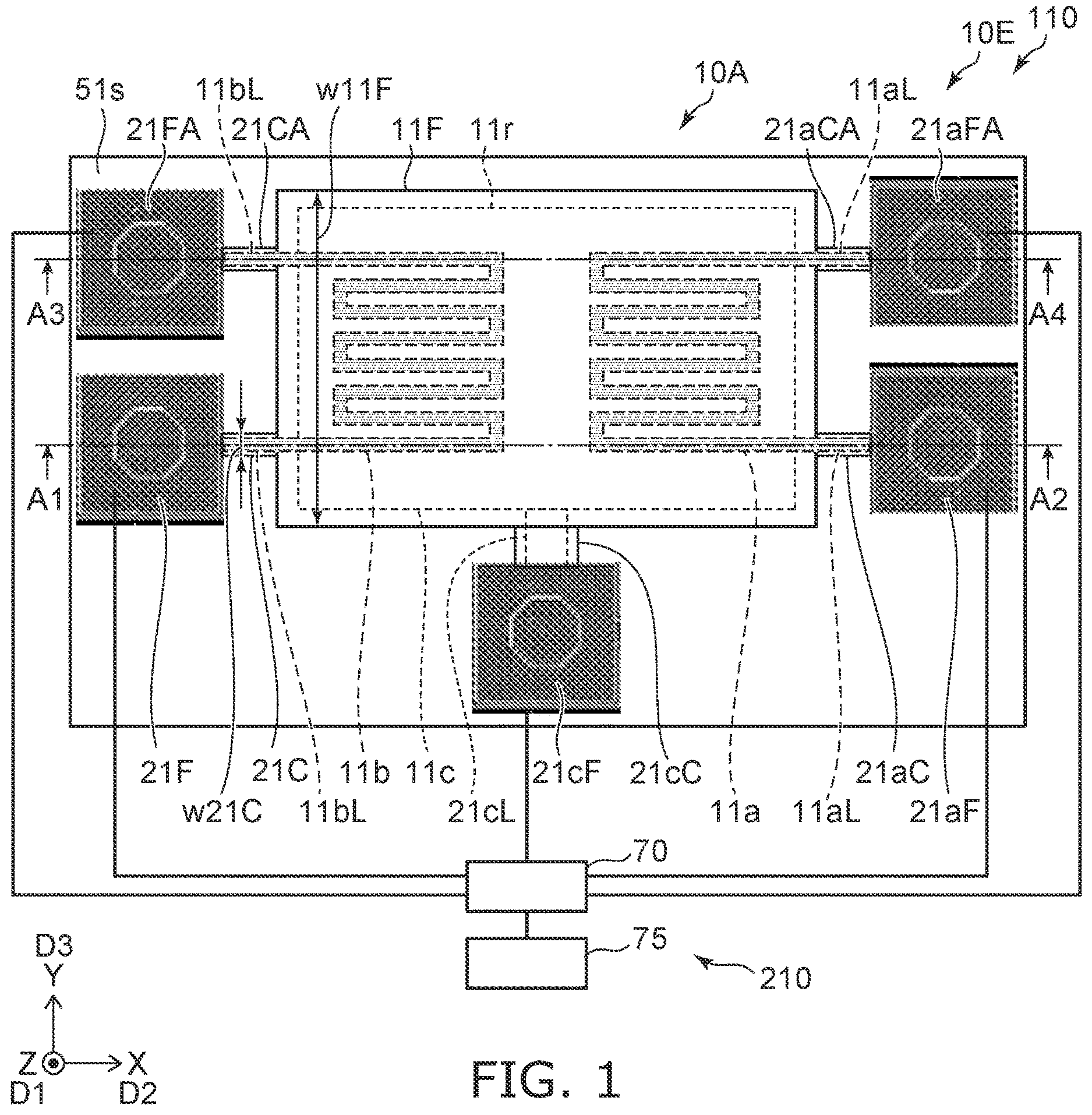
is a schematic plan view illustrating a sensor according to a first embodiment.
A and 2 B are schematic cross-sectional views illustrating the sensor according to the first embodiment.
A is a cross-sectional view taken along the line A 1 -A 2 in . B is a cross-sectional view taken along the line A 3 -A 4 of .
As shown in , 2 A and 2 B , a sensor 110 according to the embodiment includes an element section 10 E. The element section 10 E includes a first base 51 s and a first element 10 A.
The first base 51 s may include, for example, a silicon substrate. The first base 51 s may include electronic circuits such as transistors.
The first element 10 A includes a first fixed member 21 F fixed to the first base 51 s , a first connecting member 21 C supported by the first fixed member 21 F, and a first film portion 11 F supported by the first connecting member 21 C.
A first gap g 1 is provided between the first base 51 s and the first film portion 11 F. A first direction D 1 from the first base 51 s to the first fixed member 21 F is defined as a Z-axis direction. One direction perpendicular to the Z-axis direction is defined as an X-axis direction. A direction perpendicular to the Z-axis direction and the X-axis direction is defined as a Y-axis direction.
The first base 51 s includes a first face 51 F. The first face 51 F extends along the X-Y plane. The first fixed member 21 F is fixed to the first face 51 F.
The first film portion 11 F includes a first resistance layer 11 a , a first conductive layer 11 b , and a first conductive member 11 c . The first resistance layer 11 a does not overlap the first conductive layer 11 b in the first direction D 1 . The first conductive member 11 c overlaps the first resistance layer 11 a and the first conductive layer 11 b in the first direction D 1 .
By the first resistance layer 11 a , which does not overlap the first conductive layer 11 b , for example, electromagnetic coupling between the first resistance layer 11 a and the first conductive layer 11 b is suppressed.
The first electrical resistance R 1 of the first resistance layer 11 a changes depending on a state of the detection target around the first element 10 A.
As shown in , in the sensor 110 , a controller 70 may be provided. The controller 70 may be included in the sensor 110 . The controller 70 may be provided separately from the sensor 110 . The controller 70 is configured to supply a first electric power to the first conductive layer 11 b and to detect the first electrical resistance R 1 . The supply of the first electric power raises the temperature of the first film portion 11 F. By the first conductive member 11 c overlapping the first resistance layer 11 a and the first conductive layer 11 b , the heat of the first conductive layer 11 b is efficiently transmitted to the first resistance layer 11 a . The first conductive member 11 c functions as a heat conductor.
The heat of the first film portion 11 F, for example, propagates from the first film portion 11 F to its surroundings. A part of the heat propagates to the first base 51 s through the first gap g 1 . Another part of the heat propagates upward through the first film portion 11 F. The first conductive member 11 c may function as a radiator.
For example, the heat propagation (heat dissipation) changes according to the state of the detection target around the first element 10 A. The detection target is, for example, a gas. For example, the thermal conductivity of the gas around the first element 10 A depends on the elements (and/or molecules) included in the gas and their concentration. The heat dissipation property changes depending on the state of the detection target (type and concentration of gas), and as a result, the first electrical resistance R 1 of the first resistance layer 11 a changes. By detecting the first electrical resistance R 1 , it is possible to detect the state of the detection target (gas and change in concentration of gas).
Thus, in the embodiment, the first electrical resistance R 1 changes depending on the state of the detection target when the temperature of the first film portion 11 F is raised by the first electric power supplied to the first conductive layer 11 b.
The detection target exists in the first gap g 1 . The first electrical resistance R 1 changes depending on the state of the detection target between the first base 51 s and the first film portion 11 F.
In such a sensor 110 , it has been found that the signal obtained from the first resistance layer 11 a (the signal corresponding to the first electrical resistance R 1 ) tends to include noise when the first resistance layer 11 a overlaps the first conductive layer 11 b . For example, for rising the temperature, a large current is supplied to the first conductive layer 11 b . It is considered that noise included in the large current causes the noise in the signal obtained from the first resistance layer 11 a.
In the embodiment, the first resistance layer 11 a and the first conductive layer 11 b are provided so as not to overlap each other in the first direction D 1 . Thereby, coupling is suppressed and the noise is suppressed. By providing the first conductive member 11 c , the temperature of the first resistance layer 11 a can be raised efficiently and uniformly. The noise is suppressed in the signal obtained from the first resistance layer 11 a . As a result, the detection target can be detected with high accuracy. According to the embodiment, it is possible to provide a sensor capable of improving characteristics.
The potential of the first conductive member 11 c may be fixed. The potential of the first conductive member 11 c is, for example, fixed to the ground potential. Thereby, the influence on the first resistance layer 11 a from the first conductive layer 11 b via the first conductive member 11 c can be further suppressed. The noise can be suppressed more. The first conductive member 11 c whose potential is fixed functions as a shield. The detection targets can be detected with higher accuracy.
In the embodiment, for example, a first conductive layer current flowing through the first conductive layer 11 b in the supply of the first electric power is large. Thereby, the first film portion 11 F can be effectively heated. On the other hand, a first resistance layer current flowing through the first resistance layer 11 a in the detecting the first electrical resistance R 1 is relatively small. For example, the first conductive layer current is greater than the first resistance layer current.
The noise is likely to occur when the first conductive layer current is greater than the first resistance layer current. In the embodiment, even in such a state where the noise is likely to occur, the noise can be effectively suppressed by not overlapping the first resistance layer 11 a and the first conductive layer 11 b.
For example, the first conductive layer current is not less than 2 times the first resistance layer current. For example, the first conductive layer current may be not less than 5 times the first resistance layer current.
The first conductive member 11 c may be electrically connected to the first base 51 s . A first base potential of the first base 51 s may be substantially the same as the potential of the first conductive member 11 c.
As shown in A , in this example, a distance da 1 along the first direction D 1 between the first base 51 s and the first resistance layer 11 a is shorter than a distance db 1 along the first direction D 1 between the first base 51 s and the first conductive layer 11 b . The first resistance layer 11 a and the first conductive layer 11 b are located between the first base 51 s and the first conductive member 11 c . The first conductive layer 11 b spreads heat easily to the first conductive member 11 c by proximity, for example. The first resistance layer 11 a easily detects the change of the gas in the first gap g 1 by proximity in the first gap g 1 . As will be described below, the distance da 1 may be substantially the same as the distance db 1 .
In the embodiments, the electrical resistance of the first conductive layer 11 b may be lower than the electrical resistance of the first resistance layer 11 a . Efficient heating can be achieved by the first conductive layer 11 b.
The material of the first conductive layer 11 b may be substantially the same as the material of the first resistance layer 11 a . For example, the first conductive layer 11 b and the first resistance layer 11 a may include at least one selected from the group consisting of Au, Al, Ti, TiN and Pt.
As shown in , a part of the first conductive member 11 c overlaps the first conductive layer 11 b and the first resistance layer 11 a in the first direction D 1 . Another part of the first conductive member 11 c does not overlap the first conductive layer 11 b and the first resistance layer 11 a in the first direction D 1 . For example, in a plane (X-Y plane) crossing the first direction D 1 , at least a part of the outer edge 11 r of the first conductive member 11 c is outside the first conductive layer 11 b and the first resistance layer 11 a . For example, the area of the first conductive member 11 c is larger than the area of the first conductive layer 11 b and larger than the area of the first resistance layer 11 a . By such a first conductive member 11 c , temperature of the first film portion 11 F becomes more uniform.
As shown in , the first connecting member 21 C extends along a second direction D 2 . The second direction D 2 crosses the first direction D 1 . A width of the first connecting member 21 C in a third direction D 3 is defined as a first connecting member width w 21 C. The third direction D 3 crosses a plane including the first direction D 1 and the second direction D 2 . A width of the first film portion 11 F in the third direction D 3 is defined as a first film portion width w 11 F. The first connecting member width w 21 C is narrower than the first film portion width w 11 F. Thereby, it is possible to suppress the heat of the first film portion 11 F from propagating through the first connecting member 21 C. The temperature of the film can be raised with low energy consumption.
As shown in and B , the first element 10 A includes a first other fixed member 21 FA fixed to the first base 51 s and a first other connecting member 21 CA supported by the first other fixed member 21 FA. The first other connecting member 21 CA supports the first film portion 11 F. A first conductive layer wiring 11 b L electrically connected to the first conductive layer 11 b passes through the first connecting member 21 C and the first other connecting member 21 CA. The controller 70 may be electrically connected to the first conductive layer 11 b via the first conductive layer wiring 11 b L.
As shown in , A and B , the first element 10 A may further include a first resistance fixed member 21 a F fixed to the first base 51 s , a first resistance connecting member 21 a C supported by the first resistance fixed member 21 a F, a first other resistance fixed member 21 a FA fixed to the first base 51 s , and a first other resistance connecting member 21 a CA supported by the first other resistance fixed member 21 a FA.
The first resistance connecting member 21 a C and the first other resistance connecting member 21 a CA support the first film portion 11 F. The first resistance layer wiring 11 a L electrically connected to the first resistance layer 11 a passes through the first resistance connecting member 21 a C and the first other resistance connecting member 21 a CA. The controller 70 may be electrically connected to the first resistance layer 11 a via the first resistance layer wiring 11 a L.
As shown in , the first element 10 A may further include a first conductive fixed member 21 c F fixed to the first base 51 s and a first conductive connecting member 21 c C supported by the first conductive fixed member 21 c F. The first conductive connecting member 21 c C supports the first film portion 11 F. The first conductive member wiring 21 c L electrically connected to the first conductive member 11 c extends along the first conductive connecting member 21 c C. The first conductive member 11 c may be set to a fixed potential via the first conductive member wiring 21 c L.
A and 3 B are schematic cross-sectional views illustrating a sensor according to the first embodiment.
A and 3 B are cross-sectional views corresponding to the line A 1 -A 2 and the line A 3 -A 4 of .
As shown in A and 3 B , in a sensor 112 according to the embodiment, the first conductive member 11 c is located between the first base 51 s and the first resistance layer 11 a , and between the first base 51 s and the first conductive layer 11 b . Except for this, the configuration of the sensor 112 may be the same as the configuration of the sensor 110 .
By providing the first conductive member 11 c between the first base 51 s and the first resistance layer 11 a and between the first base 51 s and the first conductive layer 11 b , for example, the number of wiring layers can be reduced, and the manufacturing becomes easy.
A and 4 B are schematic cross-sectional views illustrating a sensor according to the first embodiment.
A and 4 B are cross-sectional views corresponding to the line A 1 -A 2 and the line A 3 -A 4 in .
As shown in A and 4 B , in a sensor 113 according to the embodiment, the first film portion 11 F further includes a first other conductive member 11 c A. Except for this, the configuration of the sensor 113 may be the same as the configuration of the sensor 110 .
In the sensor 113 , the first other conductive member 11 c A overlaps the first resistance layer 11 a and the first conductive layer 11 b in the first direction D 1 . The first resistance layer 11 a and the first conductive layer 11 b are provided between the first conductive member 11 c and the first other conductive member 11 c A.
For example, the potentials of the first conductive member 11 c and the first other conductive member 11 c A are fixed. The potentials of the first conductive member 11 c and the first other conductive member 11 c A may be electrically connected to the first base 51 s . The first other conductive member 11 c A has, for example, a function of a ground plane. The first conductive member 11 c has, for example, a function of a ground plane and the function of a radiator. The noise can be suppressed more. Detection with higher accuracy becomes possible.
is a schematic plan view illustrating a part of a sensor according to the first embodiment.
As shown in , in a sensor 120 according to the embodiment, the element section 10 E includes a second base 52 s and a second element 10 B in addition to the first base 51 s and the first element 10 A (omitted in ) described with respect to . In the sensor 120 , the configuration of the first base 51 s and the first element 10 A may be the same as those in the sensor 110 .
The second element 10 B includes a second fixed member 22 F fixed to the second base 52 s , a second connecting member 22 C supported by the second fixed member 22 F, and a second film portion 12 F supported by the second connecting member 22 C. The second base 52 s may be continuous with the first base 51 s . The boundary between the second base 52 s and the first base 51 s may be clear or unclear.
A second gap g 2 is provided between the second base 52 s and the second film portion 12 F. The second film portion 12 F includes a second resistance layer 12 a . The controller 70 is configured to output a value corresponding to a difference between the second electrical resistance R 2 of the second resistance layer 12 a and the first electrical resistance R 1 (see ). The controller 70 includes, for example, a differential amplifier.
The second element 10 B is, for example, a reference element. For example, influences such as fluctuations in ambient temperature are suppressed. Higher accuracy detection is possible.
In this example, the second film portion 12 F includes a second conductive layer 12 b . Power need not be supplied to the second conductive layer 12 b . The second conductive layer 12 b may not be used for the detection.
In this example, the second film portion 12 F includes a second conductive member 12 c . The second conductive member 12 c overlaps, for example, the second resistance layer 12 a and the second conductive layer 12 b . For example, the potential of the second conductive member 12 c may be fixed. By the second conductive member 12 c , the temperature of the second film portion 12 F is made uniform.
In the embodiment, the second conductive layer 12 b and the second conductive member 12 c may be omitted. Alternatively, the configuration of the second element 10 B may be substantially the same as the configuration of the first element 10 A. The first element 10 A and the second element 10 B have substantially the same heat capacity and the like, which enables detection with higher accuracy.
In the sensor 120 , the second element 10 B may further include a second other fixed member 22 FA fixed to the second base 52 s , and a second other connecting member 22 CA supported by the second other fixed member 22 FA. The second other connecting member 22 CA supports the second film portion 12 F. The second film portion 12 F is supported more stably. Power may be supplied to the second conductive layer 12 b via the second connecting member 22 C and the second other connecting member 22 CA.
In the sensor 120 , the second element 10 B may further include a second resistance fixed member 22 a F fixed to the second base 52 s , a second resistance connecting member 22 a C supported by the second resistance fixed member 22 a F, a second resistance fixed member 22 a FA fixed to the second base 52 s , and a second resistance connecting member 22 a CA supported by the second resistance fixed member 22 a FA.
The second resistance connecting member 22 a C and the second other resistance connecting member 22 a CA support the second film portion 12 F. The second electrical resistance R 2 of the second resistance layer 12 a may be detected via the second resistance connecting member 22 a C and the second other resistance connecting member 22 a CA.
Second Embodiment
The second embodiment relates to a sensor system. As shown in to 5 , sensor systems 210 , 212 , 213 , and 220 according to embodiments include sensors according to embodiments (sensors 110 , 112 , 113 , and 120 ) and a communicator 75 . The communicator 75 is configured to transmit a signal corresponding to the change in the first electrical resistance R 1 . According to embodiments, low noise sensor signals can be obtained from a remote location.
The communicator 75 is configured to supply signals to the outside, for example, by at least one of wired or wireless methods. The communicator 75 may be configured to acquire control signals from the outside. The controller 70 may be controlled by the control signal from the outside.
The embodiments may include the following configurations (for example, technical proposals).
Configuration 1
A sensor, comprising:
•
• an element section including a first base and a first element, • the first element including
• a first fixed member fixed to the first base, • a first connecting member supported by the first fixed member, and • a first film portion supported by the first connecting member, • a first gap being provided between the first base and the first film portion, • the first film portion including a first resistance layer, a first conductive layer, and a first conductive member, • the first resistance layer not overlapping the first conductive layer in a first direction from the first base to the first fixed member, • the first conductive member overlapping the first resistance layer and the first conductive layer in the first direction, • a first electrical resistance of the first resistance layer being configured to change according to a state of a detection target around the first element. Configuration 2
The sensor according to Configuration 1, wherein in a state in which a temperature of the first film portion is raised by a first electric power supplied to the first conductive layer, the first electrical resistance is configured to change depending on the state of the detection target.
Configuration 3
The sensor according to Configuration 1 or 2, wherein the first electrical resistance changes according to the state of the detection target between the first base and the first film portion.
Configuration 4
The sensor according to any one of Configurations 1-3, wherein
•
• a distance between the first base and the first resistance layer along the first direction is shorter than a distance between the first base and the first conductive layer along the first direction. Configuration 5
The sensor according to any one of Configurations 1-3, wherein
•
• a distance between the first base and the first resistance layer along the first direction is substantially the same as a distance between the first base and the first conductive layer along the first direction. Configuration 6
The sensor according to any one of Configurations 1-5, wherein
•
• the first film portion further includes a first other conductive member, • the first other conductive member overlaps the first resistance layer and the first conductive layer in the first direction, and • the first resistance layer and the first conductive layer are provided between the first conductive member and the first other conductive member. Configuration 7
The sensor according to any one of Configurations 1-6, wherein
•
• the first conductive member is electrically connected to the first base. Configuration 8
The sensor according to any one of Configurations 1-7, wherein
•
• a first base potential of the first base is substantially the same as a potential of the first conductive member. Configuration 9
The sensor according to any one of Configurations 1-8, wherein
•
• an electrical resistance of the first conductive layer is lower than an electrical resistance of the first resistance layer. Configuration 10
The sensor according to any one of Configurations 1-9, wherein
•
• at least one of the first conductive layer or the first resistance layer includes at least one selected from the group consisting of Au, Al, Ti, TiN and Pt. Configuration 11
The sensor according to any one of Configurations 1-10, wherein
•
• a part of the first conductive member overlaps the first conductive layer and the first resistance layer in the first direction, and • another part of the first conductive member does not overlap the first conductive layer and the first resistance layer in the first direction. Configuration 12
The sensor according to any one of Configurations 1-11, wherein
•
• in a plane crossing the first direction, at least a part of the outer edge of the first conductive member is outside the first conductive layer and the first resistance layer. Configuration 13
The sensor according to any one of Configurations 1-12, wherein
•
• the first connecting member extends along a second direction crossing the first direction, and • a first connecting member width of the first connecting member in a third direction crossing a plane including the first direction and the second direction is narrower than a first film portion width of the first film portion in the third direction. Configuration 14
The sensor according to any one of Configurations 1-13, wherein
•
• the first element further includes
• a first other fixed member fixed to the first base, and • a first other connecting member supported by the first other fixed member, • the first other connecting member supports the first film portion, and • a first conductive layer wiring electrically connected to the first conductive layer passes through the first connecting member and the first other connecting member. Configuration 15
The sensor according to any one of Configurations 1-14, wherein
•
• the first element further includes
• a first resistance fixed member fixed to the first base, • a first resistance connecting member supported by the first resistance fixed member, • a first resistance fixed member fixed to the first base, and • a first resistance connecting member supported by the first resistance fixed member, • the first resistance connecting member and the first other resistance connecting member support the first film portion, and • a first resistance layer wiring electrically connected to the first resistance layer passes through the first resistance connecting member and the first other resistance connecting member. Configuration 16
The sensor according to any one of Configurations 1-15, wherein
•
• the first element further includes
• a first conductive fixed member fixed to the first base, and • a first conductive connecting member supported by the first conductive fixed member. Configuration 17
The sensor according to Configuration 2, further comprising:
•
• a controller, • the controller being configured to supply a first electric power to the first conductive layer, and • the controller being configured to output a signal corresponding to the first electrical resistance. Configuration 18
The sensor according to Configuration 17, wherein
•
• a first conductive layer current through the first conductive layer in a supplying the first electric power is larger than a first resistance layer current flowing through the first resistance layer in a detecting the first electrical resistance. Configuration 19
The sensor according to Configuration 17 or 18, wherein
•
• the element section further includes a second base and a second element, • the second element includes
• a second fixed member fixed to the second base, • a second connecting member supported by the second fixed member, and • a second film portion supported by the second connecting member, • a second gap is provided between the second base and the second film portion, • the second film portion includes a second resistance layer, and • the controller is configured output a value corresponding to a difference between a second electrical resistance of the second resistance layer and the first electrical resistance. Configuration 20
A sensor system, comprising:
•
• the sensor according to Configuration 1; and • a communicator configured to transmit a signal corresponding to the change in the first electrical resistance.
According to the embodiment, a sensor and a sensor system capable of improving characteristics can be provided.
In the specification of the application, “perpendicular” and “parallel” refer to not only strictly perpendicular and strictly parallel but also include, for example, the fluctuation due to manufacturing processes, etc. It is sufficient to be substantially perpendicular and substantially parallel.
Hereinabove, exemplary embodiments of the invention are described with reference to specific examples. However, the embodiments of the invention are not limited to these specific examples. For example, one skilled in the art may similarly practice the invention by appropriately selecting specific configurations of components included in sensors and sensor systems such as, bases, element sections, fixed members, connecting members, film portions, controllers, etc., from known art. Such practice is included in the scope of the invention to the extent that similar effects thereto are obtained.
Further, any two or more components of the specific examples may be combined within the extent of technical feasibility and are included in the scope of the invention to the extent that the purport of the invention is included.
Moreover, all sensors and all sensor systems practicable by an appropriate design modification by one skilled in the art based on the sensors and the sensor systems described above as embodiments of the invention also are within the scope of the invention to the extent that the purport of the invention is included.
Various other variations and modifications can be conceived by those skilled in the art within the spirit of the invention, and it is understood that such variations and modifications are also encompassed within the scope of the invention.
While certain embodiments have been described, these embodiments have been presented by way of example only, and are not intended to limit the scope of the inventions. Indeed, the novel embodiments described herein may be embodied in a variety of other forms; furthermore, various omissions, substitutions and changes in the form of the embodiments described herein may be made without departing from the spirit of the inventions. The accompanying claims and their equivalents are intended to cover such forms or modifications as would fall within the scope and spirit of the invention.
Figures (5)
Citations
This patent cites (4)
- US3 534 154
- US2004219403
- US2017-36935
- US2019-152451