Abstract
A display device includes: a substrate including a first portion, a second portion, and a folding portion between the first and second portions; a plurality of transistors on the substrate, and located on at least the first and second portions; a plurality of inorganic insulating layers extending on the first and second portions to cover a semiconductor layer and a gate of the transistors; a plurality of light-emitting devices connected to the transistors; and a connection line on the folding portion. The inorganic insulating layers are not located on at least a part of the folding portion.
Claims (20)
1 . An electronic device comprising: a substrate comprising a first portion, a second portion, and a folding portion between the first and second portions; a plurality of transistors on the substrate, and located on at least the first and second portions; a plurality of inorganic insulating layers extending on the first and second portions to cover a semiconductor layer and a gate of the transistors; a plurality of light-emitting devices connected to the transistors; and a connection line on the folding portion, wherein the inorganic insulating layers are not located on at least a part of the folding portion, and wherein, in the at least the part of the folding portion, no inorganic material contacts the substrate.
3 . A display device comprising: a substrate comprising a first portion, a second portion, and a folding portion between the first and second portions; a plurality of transistors on the substrate, and located on at least the first and second portions; a plurality of inorganic insulating layers extending on the first and second portions to cover a semiconductor layer and a gate of the transistors; a plurality of light-emitting devices connected to the transistors; and a connection line on the folding portion, wherein the inorganic insulating layers are not located on at least a part of the folding portion, wherein the folding portion comprises: a first folding portion adjacent to the first portion; a second folding portion adjacent to the second portion; and a connecting portion between the first and second folding portions, wherein a transistor from among the plurality of transistors and a light-emitting device from among the plurality of light-emitting devices are located on the first and second folding portions, and wherein the connection line is located on the connecting portion.
Show 18 dependent claims
2 . The electronic device of claim 1 , wherein the folding portion is configured to be folded and unfolded.
4 . The display device of claim 3 , wherein the inorganic insulating layers are located on the first and second folding portions, and are not located on the connecting portion.
5 . The display device of claim 3 , wherein the plurality of transistors and the plurality of light-emitting devices are not located on the connecting portion.
6 . The display device of claim 3 , wherein the connecting portion has the greatest curvature when the folding portion is folded.
7 . The display device of claim 3 , further comprising: a first data line connected to the transistors from among the plurality of transistors that are located on the first portion and the first folding portion; and a second data line connected to the transistors from among the plurality of transistors that are located on the second portion and the second folding portion, wherein the first and second data lines are electrically connected to each other through the connection line.
8 . The display device of claim 7 , further comprising: a first organic insulating layer on the transistors located on each of the first and second portions and the first and second folding portions; a connection electrode on the first organic insulating layer; and a second organic insulating layer on the connection electrode, wherein the connection electrode is connected to a transistor from among the plurality of transistors and a light-emitting device from among the plurality of light-emitting devices.
9 . The display device of claim 8 , wherein the first and second organic insulating layers are located on the connecting portion, and wherein the first organic insulating layer is in direct contact with a top surface of the substrate at the connecting portion.
10 . The display device of claim 8 , wherein the first and second data lines and the connection line are located on the first organic insulating layer to form a single line, and the second organic insulating layer is on the connection line.
11 . The display device of claim 8 , wherein each of the light-emitting devices comprises: a first electrode on and connected to a corresponding transistor from among the plurality of transistors; a second electrode on the first electrode; and an emission layer between the first electrode and the second electrode, wherein the connection line and the first electrode are located at the same layer as each other on the second organic insulating layer.
12 . The display device of claim 3 , wherein the connection line is located on a portion of the first folding portion adjacent to the connecting portion, and on a portion of the second folding portion adjacent to the connecting portion, and wherein the connection line is connected to first and second data lines.
13 . The display device of claim 3 , further comprising: an input-sensing part on the light-emitting device, the input-sensing part comprising: a first conductive pattern; and a second conductive pattern on the first conductive pattern; a first data line on a portion of the first folding portion; a second data line on a portion of the second folding portion; and pad electrodes on and connected to the first and second data lines on the first and second folding portions, the pad electrodes being located at the same layer as that of the second conductive pattern, wherein the connection line is located on and connected to the pad electrodes.
14 . The display device of claim 13 , further comprising: a third organic insulating layer on the second conductive pattern; and a fourth organic insulating layer on the third organic insulating layer, wherein the connection line is located on the third organic insulating layer, and wherein the fourth organic insulating layer is located on the connection line.
15 . The display device of claim 14 , wherein the third organic insulating layer is in direct contact with a top surface of the substrate at the connecting portion.
16 . The display device of claim 13 , further comprising a flexible film including the connection line, wherein the flexible film is located on the pad electrodes, and wherein the connection line is connected to the pad electrodes.
17 . The display device of claim 16 , wherein the substrate is cut at the connecting portion.
18 . The display device of claim 3 , wherein a light emitting device from among the light-emitting devices is located on the connecting portion, and the light-emitting device located on the connecting portion is connected to a transistor from among the transistors located on one of the first or second folding portions.
19 . The display device of claim 3 , further comprising: a dummy substrate on the connecting portion; and a dummy light-emitting device on the dummy substrate, wherein the substrate is cut at the connecting portion, and wherein the dummy light-emitting device is connected to a transistor from among the transistors located on one of the first or second folding portions by the connection line.
20 . The display device of claim 3 , wherein the substrate is perpendicularly bent at the connecting portion.
Full Description
Show full text →
CROSS-REFERENCE TO RELATED APPLICATIONS
This application claims priority to and the benefit of Korean Patent Application No. 10-2022-0065970, filed on May 30, 2022, in the Korean Intellectual Property Office, the entire content of which is incorporated by reference herein.
BACKGROUND
1. Field
Aspects of embodiments of the present disclosure relate to a display device.
2. Description of the Related Art
In general, a display device includes a display module to display an image, and a supporting part to support the display module. The display module includes a display panel to display an image, a window disposed on the display panel to protect the display panel from an external scratch and/or impact, and a protection layer disposed below the display panel to protect the display panel from an external impact. The supporting part may have higher hardness than that of the display module, and may support the display module.
A flexible display device includes a flexible display module, which may be bent or rolled. A foldable display module, which is an example of the flexible display module, may be folded and/or unfolded along a folding axis. A display module includes a substrate, a transistor disposed on the substrate, and a light-emitting device disposed on the transistor. Inorganic insulating layers are disposed on the substrate to cover the transistors.
The above information disclosed in this Background section is for enhancement of understanding of the background of the present disclosure, and therefore, it may contain information that does not constitute prior art.
SUMMARY
When a display device is folded, stress may be concentrated to inorganic insulating layers to cause a crack in an inorganic layer, which may be vulnerable to a mechanical stress, and thus, a folding portion of a display module may be damaged. Accordingly, a display device capable of preventing or substantially preventing damage to the folding portion may be desired.
One or more embodiments of the present disclosure are directed to a display device that may prevent or substantially prevent a folding portion from being damaged.
According to one or more embodiments of the present disclosure, a display device includes: a substrate including a first portion, a second portion, and a folding portion between the first and second portions; a plurality of transistors on the substrate, and located on at least the first and second portions; a plurality of inorganic insulating layers extending on the first and second portions to cover a semiconductor layer and a gate of the transistors; a plurality of light-emitting devices connected to the transistors; and a connection line on the folding portion. The inorganic insulating layers are not located on at least a part of the folding portion.
In an embodiment, the folding portion may be configured to be folded and unfolded.
In an embodiment, the folding portion may include: a first folding portion adjacent to the first portion; a second folding portion adjacent to the second portion; and a connecting portion between the first and second folding portions. A transistor from among the plurality of transistors and a light-emitting device from among the plurality of light-emitting devices may be located on the first and second folding portions, and the connection line may be located on the connecting portion.
In an embodiment, the inorganic insulating layers may be located on the first and second folding portions, and may not be located on the connecting portion.
In an embodiment, the plurality of transistors and the plurality of light-emitting devices may not be located on the connecting portion.
In an embodiment, the connecting portion may have the greatest curvature when the folding portion is folded.
In an embodiment, the display device may further include: a first data line connected to the transistors from among the plurality of transistors that are located on the first portion and the first folding portion; and a second data line connected to the transistors from among the plurality of transistors that are located on the second portion and the second folding portion. The first and second data lines may be electrically connected to each other through the connection line.
In an embodiment, the display device may further include: a first organic insulating layer on the transistors located on each of the first and second portions and the first and second folding portions; a connection electrode on the first organic insulating layer; and a second organic insulating layer on the connection electrode. The connection electrode may be connected to a transistor from among the plurality of transistors and a light-emitting device from among the plurality of light-emitting devices.
In an embodiment, the first and second organic insulating layers may be located on the connecting portion, and the first organic insulating layer may be in direct contact with a top surface of the substrate at the connecting portion.
In an embodiment, the first and second data lines and the connection line may be located on the first organic insulating layer to form a single line, and the second organic insulating layer may be on the connection line.
In an embodiment, each of the light-emitting devices may include: a first electrode on and connected to a corresponding transistor from among the plurality of transistors; a second electrode on the first electrode; and an emission layer between the first electrode and the second electrode. The connection line and the first electrode may be located at the same layer as each other on the second organic insulating layer.
In an embodiment, the connection line may be located on a portion of the first folding portion adjacent to the connecting portion, and on a portion of the second folding portion adjacent to the connecting portion, and the connection line may be connected to first and second data lines.
In an embodiment, the display device may further include: an input-sensing part on the light-emitting device, the input-sensing part including: a first conductive pattern; and a second conductive pattern on the first conductive pattern; a first data line on a portion of the first folding portion; a second data line on a portion of the second folding portion; and pad electrodes on and connected to the first and second data lines on the first and second folding portions, the pad electrodes being located at the same layer as that of the second conductive pattern. The connection line may be located on and connected to the pad electrodes.
In an embodiment, the display device may further include: a third organic insulating layer on the second conductive pattern; and a fourth organic insulating layer on the third organic insulating layer. The connection line may be located on the third organic insulating layer, and the fourth organic insulating layer may be located on the connection line.
In an embodiment, the third organic insulating layer may be in direct contact with a top surface of the substrate at the connecting portion.
In an embodiment, the display device may further include a flexible film including the connection line. The flexible film may be located on the pad electrodes, and the connection line may be connected to the pad electrodes.
In an embodiment, the substrate may be cut at the connecting portion.
In an embodiment, a light emitting device from among the light-emitting devices may be located on the connecting portion, and the light-emitting device located on the connecting portion may be connected to a transistor from among the transistors located on one of the first or second folding portions.
In an embodiment, the display device may further include: a dummy substrate on the connecting portion; and a dummy light-emitting device on the dummy substrate. The substrate may be cut at the connecting portion, and the dummy light-emitting device may be connected to a transistor from among the transistors located on one of the first or second folding portions by the connection line.
In an embodiment, the substrate may be perpendicularly bent at the connecting portion.
BRIEF DESCRIPTION OF THE DRAWINGS
The above and other aspects and features of the present disclosure will be more clearly understood from the following detailed description of the illustrative, non-limiting embodiments with reference to the accompanying drawings.
is a perspective view illustrating a display device according to an embodiment of the present disclosure.
is a perspective view illustrating the display device of in a folding state.
is a sectional view illustrating a display module.
is a sectional view illustrating a display panel of .
is a sectional view illustrating a portion of a display panel corresponding to a folding region, and non-folding regions adjacent to the folding region shown in .
is a sectional view illustrating the display panel of in a folding state.
is a plan view illustrating the display panel of .
is a sectional view illustrating a portion of a display panel corresponding to one of the pixels of a first portion of .
is an enlarged view illustrating the region AA 3 of .
is a sectional view illustrating pixels of a connecting portion, and first and second folding portions adjacent to the connecting portion shown in .
is a sectional view illustrating a display panel according to an embodiment of the present disclosure.
is a sectional view illustrating a display panel according to an embodiment of the present disclosure.
is a sectional view illustrating a display panel according to an embodiment of the present disclosure.
is a sectional view illustrating a display panel according to an embodiment of the present disclosure.
is an enlarged view illustrating a substrate according to an embodiment of the present disclosure.
is a sectional view illustrating pixels of a connecting portion, and first and second folding portions adjacent to the connecting portion shown in .
is a sectional view illustrating a display panel according to an embodiment of the present disclosure.
is a perspective view illustrating a display device according to an embodiment of the present disclosure.
is a diagram illustrating a display panel viewed in a first direction of the display device of .
DETAILED DESCRIPTION
Hereinafter, embodiments will be described in more detail with reference to the accompanying drawings, in which like reference numbers refer to like elements throughout. The present disclosure, however, may be embodied in various different forms, and should not be construed as being limited to only the illustrated embodiments herein. Rather, these embodiments are provided as examples so that this disclosure will be thorough and complete, and will fully convey the aspects and features of the present disclosure to those skilled in the art. Accordingly, processes, elements, and techniques that are not necessary to those having ordinary skill in the art for a complete understanding of the aspects and features of the present disclosure may not be described. Unless otherwise noted, like reference numerals denote like elements throughout the attached drawings and the written description, and thus, redundant description thereof may not be repeated.
Example embodiments of the present disclosures are described herein with reference to cross-sectional illustrations that are schematic illustrations of idealized embodiments (and intermediate structures) of example embodiments. As such, variations from the shapes of the illustrations as a result, for example, of manufacturing techniques and/or tolerances, are to be expected. Thus, example embodiments of the present disclosures should not be construed as limited to the particular shapes of regions illustrated herein, but are to include deviations in shapes that result, for example, from manufacturing.
When a certain embodiment may be implemented differently, a specific process order may be different from the described order. For example, two consecutively described processes may be performed at the same or substantially at the same time, or may be performed in an order opposite to the described order.
In the drawings, the relative sizes, thicknesses, and ratios of elements, layers, and regions may be exaggerated and/or simplified for clarity. Spatially relative terms, such as “beneath,” “below,” “lower,” “under,” “above,” “upper,” and the like, may be used herein for ease of explanation to describe one element or feature's relationship to another element(s) or feature(s) as illustrated in the figures. It will be understood that the spatially relative terms are intended to encompass different orientations of the device in use or in operation, in addition to the orientation depicted in the figures. For example, if the device in the figures is turned over, elements described as “below” or “beneath” or “under” other elements or features would then be oriented “above” the other elements or features. Thus, the example terms “below” and “under” can encompass both an orientation of above and below. The device may be otherwise oriented (e.g., rotated 90 degrees or at other orientations) and the spatially relative descriptors used herein should be interpreted accordingly.
In the figures, the x-axis, the y-axis, and the z-axis are not limited to three axes of the rectangular coordinate system, and may be interpreted in a broader sense. For example, the x-axis, the y-axis, and the z-axis may be perpendicular to or substantially perpendicular to one another, or may represent different directions from each other that are not perpendicular to one another.
It will be understood that, although the terms “first,” “second,” “third,” etc., may be used herein to describe various elements, components, regions, layers and/or sections, these elements, components, regions, layers and/or sections should not be limited by these terms. These terms are used to distinguish one element, component, region, layer or section from another element, component, region, layer or section. Thus, a first element, component, region, layer or section described below could be termed a second element, component, region, layer or section, without departing from the spirit and scope of the present disclosure.
It will be understood that when an element or layer is referred to as being “on,” “connected to,” or “coupled to” another element or layer, it can be directly on, connected to, or coupled to the other element or layer, or one or more intervening elements or layers may be present. Similarly, when a layer, an area, or an element is referred to as being “electrically connected” to another layer, area, or element, it may be directly electrically connected to the other layer, area, or element, and/or may be indirectly electrically connected with one or more intervening layers, areas, or elements therebetween. In addition, it will also be understood that when an element or layer is referred to as being “between” two elements or layers, it can be the only element or layer between the two elements or layers, or one or more intervening elements or layers may also be present. Other terms used to describe relationships between elements or layers should be interpreted in a like fashion (e.g., “adjacent” versus “directly adjacent”).
The terminology used herein is for the purpose of describing particular embodiments and is not intended to be limiting of the present disclosure. As used herein, the singular forms “a” and “an” are intended to include the plural forms as well, unless the context clearly indicates otherwise. It will be further understood that the terms “comprises,” “comprising,” “includes,” “including,” “has,” “have,” and “having,” when used in this specification, specify the presence of the stated features, integers, steps, operations, elements, and/or components, but do not preclude the presence or addition of one or more other features, integers, steps, operations, elements, components, and/or groups thereof. As used herein, the term “and/or” includes any and all combinations of one or more of the associated listed items. For example, the expression “A and/or B” denotes A, B, or A and B. Expressions such as “at least one of,” when preceding a list of elements, modify the entire list of elements and do not modify the individual elements of the list. For example, the expression “at least one of a, b, or c,” “at least one of a, b, and c,” and “at least one selected from the group consisting of a, b, and c” indicates only a, only b, only c, both a and b, both a and c, both b and c, all of a, b, and c, or variations thereof.
As used herein, the term “substantially,” “about,” and similar terms are used as terms of approximation and not as terms of degree, and are intended to account for the inherent variations in measured or calculated values that would be recognized by those of ordinary skill in the art. Further, the use of “may” when describing embodiments of the present disclosure refers to “one or more embodiments of the present disclosure.” As used herein, the terms “use,” “using,” and “used” may be considered synonymous with the terms “utilize,” “utilizing,” and “utilized,” respectively. Also, the term “exemplary” is intended to refer to an example or illustration.
Unless otherwise defined, all terms (including technical and scientific terms) used herein have the same meaning as commonly understood by one of ordinary skill in the art to which the present disclosure belongs. It will be further understood that terms, such as those defined in commonly used dictionaries, should be interpreted as having a meaning that is consistent with their meaning in the context of the relevant art and/or the present specification, and should not be interpreted in an idealized or overly formal sense, unless expressly so defined herein.
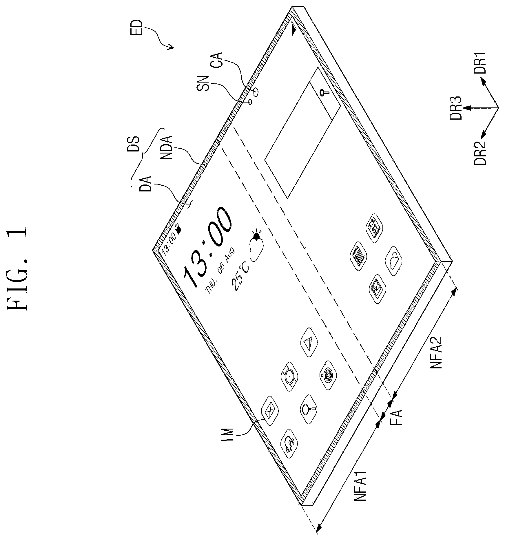
is a perspective view illustrating a display device according to an embodiment of the present disclosure.
Referring to , a display device ED according to an embodiment of the present disclosure may have a rectangular shape having long sides that are parallel to or substantially parallel to a first direction DR 1 , and short sides that are parallel to or substantially parallel to a second direction DR 2 crossing the first direction DR 1 . However, the present disclosure is not limited thereto, and in an embodiment, the display device ED may have various suitable shapes, such as a circular shape, or another suitable polygonal shape. The display device ED may be a flexible display device.
Hereinafter, a direction that is perpendicular to or substantially perpendicular to both of the first and second directions DR 1 and DR 2 will be referred to as a third direction DR 3 . Furthermore, the expressions “when viewed in a plan view” or “in a plan view” as used in the present specification describe a structure that is viewed in or from the third direction DR 3 .
The display device ED may include a folding region FA, and a plurality of non-folding regions NFA 1 and NFA 2 . The non-folding regions NFA 1 and NFA 2 may include a first non-folding region NFA 1 and a second non-folding region NFA 2 . The folding region FA may be disposed between the first and second non-folding regions NFA 1 and NFA 2 . The folding region FA, the first non-folding region NFA 1 , and the second non-folding region NFA 2 may be arranged along the second direction DR 2 .
Although one folding region FA and two non-folding regions NFA 1 and NFA 2 are illustrated for convenience, the numbers of the folding region FA and the non-folding regions NFA 1 and NFA 2 are not limited thereto. For example, the display device ED may include two or more non-folding regions, and a plurality of folding regions disposed between the non-folding regions.
A top surface of the display device ED may be referred to as a display surface DS, and the display surface DS may have a flat or substantially flat surface defined by the first and second directions DR 1 and DR 2 . Images IM generated by the display device ED may be provided to a user through the display surface DS.
The display surface DS may include a display region DA, and a non-display region NDA around (e.g., adjacent to) the display region DA. The display region DA may be used to display an image, and the non-display region NDA may not display an image. The non-display region NDA may be disposed to enclose (e.g., to surround around a periphery of) the display region DA, and may define an edge of the display device ED, which is printed with a desired color (e.g., a predetermined or specific color).
The display device ED may include at least one sensor SN, and at least one camera CA. The sensor SN and the camera CA may be adjacent to an edge portion of the display device ED. The sensor SN and the camera CA may be disposed at (e.g., in or on) the display region DA adjacent to the non-display region NDA. The sensor SN and the camera CA may be disposed at (e.g., in or on) the second non-folding region NFA 2 , but the present disclosure is not limited thereto. For example, the sensor SN and the camera CA may be disposed at (e.g., in or on) the first non-folding region NFA 1 .
Light may pass through portions of the display device ED, in which the sensor SN and the camera CA are disposed, and may be provided to the camera CA and the sensor SN. In an embodiment, the sensor SN may be an optical proximity sensor, but the kind of the sensor SN is not limited thereto. The camera CA may be configured to obtain an image of an external object. The sensor SN and the camera CA may be provided in a plurality.
is a perspective view illustrating the display device of in a folding state.
Referring to , the display device ED may be a foldable display device, which may be folded and/or unfolded. For example, when the display device ED is folded, the folding region FA may be bent along a folding axis FX that is parallel to or substantially parallel to the first direction DR 1 . In other words, the folding axis FX may be defined as a long axis that is parallel to or substantially parallel to the long side of the display device ED.
When the display device ED is folded, the display device ED may be folded in an in-folding manner, such that the first and second non-folding regions NFA 1 and NFA 2 face each other, and the display surface DS is not exposed to the outside. However, the present disclosure is not limited thereto. For example, the display device ED may be folded along the folding axis FX in an out-folding manner, such that the display surface DS is exposed to the outside.
As shown in , a distance between the first and second non-folding regions NFA 1 and NFA 2 may be equal to or substantially equal to a curvature radius R 1 .
is a sectional view illustrating a display module of .
A section (e.g., a cross-section) of the display device ED in the second direction DR 2 is illustrated as an example in .
A display module (e.g., a display or a touch-display) DM may include a display panel DP, an input-sensing part (e.g., an input sensor, an input sensing layer, or an input sensing panel) ISP, an anti-reflection layer RPL, a window WIN, a panel protection film PF, and first to third adhesive layers AL 1 -AL 3 .
The display panel DP may be a flexible display panel. In an embodiment, the display panel DP may be a light-emitting type display panel, but the present disclosure is not limited to a specific kind of the display panel DP. For example, the display panel DP may be an organic light emitting display panel or an inorganic light-emitting display panel. An emission layer of the organic light emitting display panel may include an organic light emitting material. An emission layer of the inorganic light-emitting display panel may include quantum dots or quantum rods.
The input-sensing part ISP may be disposed on the display panel DP. The input-sensing part ISP may include a plurality of sensor units (e.g., sensors or sensor electrodes), which are configured to sense an external input in an electrostatic capacitance manner. When the display device ED is fabricated, the input-sensing part ISP may be directly formed on the display panel DP. However, the present disclosure is not limited thereto, and in an embodiment, the input-sensing part ISP may be fabricated as a panel that is distinct from the display panel DP, and may then be attached to the display panel DP by an adhesive layer.
The anti-reflection layer RPL may be disposed on the input-sensing part ISP. The anti-reflection layer RPL may be defined as an anti-reflection film to external light. The anti-reflection layer RPL may be configured to reduce reflectance of the external light, which is incident into the display panel DP from the outside of the display device ED.
In a case when the display panel DP, like a mirror, reflects external light toward a user, the user may recognize the external light. In order to prevent or reduce such reflectance of the external light, the anti-reflection layer RPL may include a plurality of color filters for displaying the same or substantially the same colors as those of the pixels of the display panel DP.
The color filters may be configured to filter the external light having the same or substantially the same colors as those of the pixels. In this case, the external light may not be recognized by a user. However, the present disclosure is not limited thereto, and in an embodiment, the anti-reflection layer RPL may include a polarization film, which may include a phase retarder and/or a polarizer, and is configured to lower the reflectance of external light.
The window WIN may be disposed on the anti-reflection layer RPL. The window WIN may protect the display panel DP, the input-sensing part ISP, and the anti-reflection layer RPL from an external scratch and/or impact.
The panel protection film PF may be disposed below (e.g., underneath) the display panel DP. The panel protection film PF may protect a bottom portion of the display panel DP. The panel protection film PF may be formed of or may include a flexible plastic material (e.g., such as polyethylene terephthalate (PET)).
The first adhesive layer AL 1 may be disposed between the display panel DP and the panel protection film PF. The display panel DP and the panel protection film PF may be bonded to each other by the first adhesive layer AL 1 . However, the present disclosure is not limited thereto, and in an embodiment, the panel protection film PF may be directly formed below (e.g., underneath) the display panel DP.
The second adhesive layer AL 2 may be disposed between the anti-reflection layer RPL and the input-sensing part ISP. The anti-reflection layer RPL and the input-sensing part ISP may be bonded to each other by the second adhesive layer AL 2 . However, the present disclosure is not limited thereto, and in an embodiment, the anti-reflection layer RPL may be directly formed on the input-sensing part ISP.
The third adhesive layer AL 3 may be disposed between the window WIN and the anti-reflection layer RPL. The window WIN and the anti-reflection layer RPL may be bonded to each other by the third adhesive layer AL 3 . However, the present disclosure is not limited thereto, and in an embodiment, the window WIN may be directly formed on the anti-reflection layer RPL.
is a sectional view illustrating a display panel of .
A section (e.g., a cross-section) of the display panel DP in the second direction DR 2 is illustrated as an example in .
Referring to , the display panel DP may include a substrate SUB, a circuit device layer DP-CL disposed on the substrate SUB, a display device layer DP-OLED disposed on the circuit device layer DP-CL, and a thin encapsulation layer TFE disposed on the display device layer DP-OLED.
The substrate SUB may include the display region DA, and the non-display region NDA around (e.g., adjacent to) the display region DA. The substrate SUB may be formed of or may include a flexible plastic material (e.g., such as poly imide (PI)). The display device layer DP-OLED may be disposed at (e.g., in or on) the display region DA.
A plurality of pixels may be disposed at (e.g., in or on) the display region DA. Each of the pixels may include a light-emitting device, which is disposed in the display device layer DP-OLED, and is connected to a transistor in the circuit device layer DP-CL.
The thin encapsulation layer TFE may be disposed on the circuit device layer DP-CL to cover the display device layer DP-OLED. The thin encapsulation layer TFE may include inorganic layers, and an organic layer between the inorganic layers. The inorganic layers may protect the pixels from moisture and/or oxygen. The organic layer may protect pixels PX from a contamination material, such as dust particles.
is a sectional view illustrating a portion of a display panel corresponding to a folding region, and non-folding regions adjacent to the folding region shown in .
In the embodiment illustrated in , the substrate SUB, the circuit device layer DP-CL, the display device layer DP-OLED, the thin encapsulation layer TFE, and the input-sensing part ISP may be the same or substantially the same as those described above with reference to , and thus, redundant description thereof may not be repeated.
When viewed in the first direction DR 1 , the display panel DP may include the folding region FA, and the first and second non-folding regions NFA 1 and NFA 2 , similarly to the display device ED of . The folding region FA may be disposed between the first and second non-folding regions NFA 1 and NFA 2 . The folding region FA, the first non-folding region NFA 1 , and the second non-folding region NFA 2 may be arranged along the second direction DR 2 .
The substrate SUB may include a first portion PT 1 , a second portion PT 2 , and a folding portion FP. When viewed in a plan view, the first portion PT 1 of the substrate SUB may overlap with the first non-folding region NFA 1 of the display panel DP. When viewed in a plan view, the second portion PT 2 of the substrate SUB may overlap with the second non-folding region NFA 2 of the display panel DP. When viewed in a plan view, the folding portion FP of the substrate SUB may overlap with the folding region FA of the display panel DP. The folding portion FP may be folded and unfolded, similar to the folding region FA.
The folding portion FP may include a connecting portion CPP, a first folding portion FP 1 , and a second folding portion FP 2 . The connecting portion CPP may be disposed between the first and second folding portions FP 1 and FP 2 . The connecting portion CPP, the first folding portion FP 1 , and the second folding portion FP 2 may be arranged along the second direction DR 2 .
The first folding portion FP 1 may be adjacent to the first portion PT 1 . The second folding portion FP 2 may be adjacent to the second portion PT 2 . The connecting portion CPP may be disposed between the first and second folding portions FP 1 and FP 2 . The first folding portion FP 1 may be disposed between the connecting portion CPP and the first portion PT 1 . The second folding portion FP 2 may be disposed between the connecting portion CPP and the second portion PT 2 .
A stacking structure of the folding region FA will be described in more detail below with reference to .
is a sectional view illustrating the display panel DP of in a folding state.
Referring to , when the folding region FA is folded to fold the display panel DP, the second non-folding region NFA 2 may face the first non-folding region NFA 1 . When the display panel DP is folded, the folding portion FP may be folded. When the folding portion FP is folded, the first portion PT 1 may be disposed to face the second portion PT 2 . Thus, the first portion PT 1 may overlap with the second portion PT 2 , when viewed in the third direction DR 3 . In addition, the second folding portion FP 2 may face the first folding portion FP 1 , and may overlap with the first folding portion FP 1 .
When the display panel DP is folded, the folding portion FP may be bent to have a suitable curvature (e.g., a predetermined or specific curvature). For example, the first and second folding portions FP 1 and FP 2 may be bent to have a suitable curvature (e.g., a predetermined or specific curvature), and the connecting portion CPP may be bent to have a suitable curvature (e.g., a predetermined or specific curvature). The curvature of the connecting portion CPP may be greater than the curvatures of the first and second folding portions FP 1 and FP 2 . When the folding portion FP is folded, the connecting portion CPP may be bent more sharply. In other words, when the folding portion FP is folded, the connecting portion CPP may have the largest curvature.
is a plan view illustrating the display panel of .
Referring to , the display device ED may include the display panel DP, a scan driver SDV, a data driver DDV, and an emission driver EDV.
The display panel DP may include a first region AA 1 , a second region AA 2 , and a bending region BA between the first and second regions AA 1 and AA 2 . The bending region BA may be extended in the first direction DR 1 , and the first region AA 1 , the bending region BA, and the second region AA 2 may be arranged along the second direction DR 2 .
The first region AA 1 may include the display region DA, and the non-display region NDA near (e.g., adjacent to) the display region DA. The non-display region NDA may be provided to enclose (e.g., to surround around a periphery of) the display region DA. The display region DA may be a region used to display an image, and the non-display region NDA may be a region that does not display an image. The second region AA 2 and the bending region BA may not display an image.
The first region AA 1 may include the first non-folding region NFA 1 , the second non-folding region NFA 2 , and the folding region FA between the first and second non-folding regions NFA 1 and NFA 2 , when viewed in the third direction DR 3 . A portion of the substrate SUB overlapping with the folding region FA may include the first folding portion FP 1 , the connecting portion CPP, and the second folding portion FP 2 .
The display panel DP may include a plurality of pixels PX, a plurality of scan lines SL 1 -SLm, a plurality of data lines DL 1 -DLn, a plurality of emission lines EL 1 -ELm, first and second control lines CSL 1 and CSL 2 , a power line PL, connection lines CNL, and a plurality of pads PD. Here, m and n may be natural numbers. The pixels PX may be disposed at (e.g., in or on) the display region DA, and may be connected to the scan lines SL 1 -SLm, the data lines DL 1 -DLn, and the emission lines EL 1 -ELm. The pixels PX may not be disposed at (e.g., in or on) a portion of the display panel DP overlapping with the folding portion FP of the substrate SUB, which will be described in more detail below.
The scan driver SDV and the emission driver EDV may be disposed at (e.g., in or on) the non-display region NDA. The scan driver SDV and the emission driver EDV may be disposed at (e.g., in or on) two regions, respectively, of the non-display region NDA. The two regions may be opposite to each other in the first direction DR 1 , and may be located at opposite sides of the first region AA 1 relative to the display region DA. The data driver DDV may be disposed at (e.g., in or on) the second region AA 2 . The data driver DDV may be fabricated in the form of an integrated circuit chip, and may be mounted on the second region AA 2 .
The scan lines SL 1 -SLm may be extended in the first direction DR 1 , and may be connected to the scan driver SDV. The data lines DL 1 -DLn may be extended in the second direction DR 2 , and may be connected to the data driver DDV via the bending region BA. The data lines DL 1 -DLn may be connected to each other through a connection line CPD (e.g., see ) at (e.g., in or on) a region of the display panel DP overlapping with the connecting portion CPP of the substrate SUB. The emission lines EL 1 -Elm may be extended in the first direction DR 1 , and may be connected to the emission driver EDV.
The power line PL may be extended in the second direction DR 2 , and may be disposed at (e.g., in or on) the non-display region NDA. The power line PL may be disposed between the display region DA and the emission driver EDV, but the present disclosure is not limited thereto. For example, the power line PL may be disposed between the display region DA and the scan driver SDV.
The power line PL may be extended into the second region AA 2 through the bending region BA. The power line PL may be extended toward a lower end of the second region AA 2 , when viewed in a plan view. The power line PL may receive a driving voltage.
The connection lines CNL may be extended in the first direction DR 1 , and may be arranged along the second direction DR 2 . The connection lines CNL may be connected to the power line PL and the pixels PX. The driving voltage may be applied to the pixels PX through the power line PL and the connection lines CNL, which are connected to each other.
The first control line CSL 1 may be connected to the scan driver SDV, and may be extended toward the lower end of the second region AA 2 via the bending region BA. The second control line CSL 2 may be connected to the emission driver EDV, and may be extended toward the lower end of the second region AA 2 via the bending region BA. The data driver DDV may be disposed between the first control line CSL 1 and the second control line CSL 2 .
When viewed in a plan view, the pads PD may be disposed adjacent to the lower portion of the second region AA 2 . The data driver DDV, the power line PL, the first control line CSL 1 , and the second control line CSL 2 may be connected to the pads PD.
The data lines DL 1 -DLn may be connected to corresponding ones of the pads PD through the data driver DDV. For example, the data lines DL 1 -DLn may be connected to the data driver DDV, and the data driver DDV may be connected to the pads PD corresponding to the data lines DL 1 -DLn, respectively.
A printed circuit board may be connected to the pads PD, and a timing controller and a voltage generator may be disposed on the printed circuit board. The timing controller may be fabricated in the form of an integrated circuit chip, and may be mounted on the printed circuit board. The timing controller and the voltage generator may be connected to the pads PD through the printed circuit board.
The timing controller may control operations of the scan driver SDV, the data driver DDV, and the emission driver EDV. The timing controller may generate a scan control signal, a data control signal, and an emission control signal, in response to control signals transmitted from the outside. The voltage generator may be configured to generate the driving voltage.
The scan control signal may be provided to the scan driver SDV through the first control line CSL 1 . The emission control signal may be provided to the emission driver EDV through the second control line CSL 2 . The data control signal may be provided to the data driver DDV. The timing controller may receive image signals from the outside, may convert the image signals to data in a data format, which is suitable for interface specifications used by the data driver DDV, and may provide the converted data to the data driver DDV.
The scan driver SDV may generate a plurality of scan signals in response to the scan control signal. The scan signals may be applied to the pixels PX through the scan lines SL 1 -SLm. The scan signals may be sequentially applied to the pixels PX.
The data driver DDV may generate a plurality of data voltages, which correspond to the image signals, in response to the data control signal. The data voltages may be applied to the pixels PX through the data lines DL 1 -DLn. The emission driver EDV may generate a plurality of emission signals in response to the emission control signal. The emission signals may be applied to the pixels PX through the emission lines EL 1 -ELm.
The pixels PX may receive the data voltages in response to the scan signals. The pixels PX may be configured to emit light, which has a desired brightness level corresponding to the data voltage, in response to the emission signals, and thereby, may display an image. A light-emitting time of the pixels PX may be controlled by the emission signals.
is a sectional view illustrating a portion of a display panel corresponding to one of the pixels of a first portion of .
Referring to , the pixel PX may include a transistor TR and a light-emitting device OLED. The light-emitting device OLED may include a first electrode or anode AE, a second electrode or cathode CE, a hole control layer HCL, an electron control layer ECL, and an emission layer EL.
The transistor TR and the light-emitting device OLED may be disposed on the substrate SUB. One transistor TR is illustrated as an example, but the present disclosure is not limited thereto, and in an embodiment, the pixel PX may include a plurality of transistors, which are used to drive the light-emitting device OLED, and at least one capacitor.
The display region DA may include a light-emitting region LA, which corresponds to each of the pixels PX, and a non-light-emitting region NLA, which is provided around (e.g., adjacent to) the light-emitting region LA. The light-emitting device OLED may be disposed at (e.g., in or on) the light-emitting region LA.
A buffer layer BFL may be disposed on the substrate SUB, and in an embodiment, the buffer layer BFL may be an inorganic layer. A semiconductor pattern may be disposed on the buffer layer BFL. The semiconductor pattern may be formed of or may include at least one of poly silicon, amorphous silicon, or one or more suitable metal oxide materials.
The semiconductor pattern may be doped with an n-type dopant or a p-type dopant. The semiconductor pattern may include a highly-doped region and a lightly-doped region. The highly-doped region may have higher conductivity than that of the lightly-doped region, and may be used or substantially used as a source or drain electrode of the transistor TR. The lightly-doped region may be used or substantially used as an active (or channel) region of a transistor.
A source S, an active A, and a drain D of the transistor TR may be formed from the semiconductor pattern. A first insulating layer INS 1 may be disposed on the semiconductor pattern. A gate G of the transistor TR may be disposed on the first insulating layer INS 1 . A second insulating layer INS 2 may be disposed on the gate G. A third insulating layer INS 3 may be disposed on the second insulating layer INS 2 .
A connection electrode CNE may include a first connection electrode CNE 1 and a second connection electrode CNE 2 , which connect the transistor TR to the light-emitting device OLED. The first connection electrode CNE 1 may be disposed on the third insulating layer INS 3 , and may be connected to the drain D through a first contact hole CH 1 defined in (e.g., penetrating) the first to third insulating layers INS 1 -INS 3 .
A fourth insulating layer INS 4 may be disposed on the first connection electrode CNE 1 . In an embodiment, the first to fourth insulating layers INS 1 -INS 4 may be inorganic insulating layers. A fifth insulating layer INS 5 may be disposed on the fourth insulating layer INS 4 . The fifth insulating layer INS 5 may be an organic insulating layer. Hereinafter, the fifth insulating layer INS 5 may be referred to as a first organic insulating layer INS 5 . The second connection electrode CNE 2 may be disposed on the first organic insulating layer INS 5 . The second connection electrode CNE 2 may be connected to the first connection electrode CNE 1 through a second contact hole CH 2 defined in (e.g., penetrating) the fourth and fifth insulating layers INS 4 and INS 5 .
A sixth insulating layer INS 6 may be disposed on the second connection electrode CNE 2 . The sixth insulating layer INS 6 may be an organic insulating layer. Hereinafter, the sixth insulating layer INS 6 may be referred to as a second organic insulating layer INS 6 . A structure including the buffer layer BFL, the second organic insulating layer INS 6 , and the layers therebetween may be defined as the circuit device layer DP-CL.
The first electrode AE may be disposed on the second organic insulating layer INS 6 . The first electrode AE may be connected to the second connection electrode CNE 2 through a third contact hole CH 3 defined in (e.g., penetrating) the sixth insulating layer INS 6 . A pixel definition layer PDL may be disposed on the first electrode AE and the sixth insulating layer INS 6 . An opening PX_OP exposing a portion of the first electrode AE may be defined in (e.g., may penetrate) the pixel definition layer PDL.
The hole control layer HCL may be disposed on the first electrode AE and the pixel definition layer PDL. The hole control layer HCL may include a hole transport layer and/or a hole injection layer.
The emission layer EL may be disposed on the hole control layer HCL. The emission layer EL may be disposed in a region corresponding to the opening PX_OP. The emission layer EL may be formed of or may include at least one of various suitable organic and/or inorganic materials. The emission layer EL may be configured to emit one of red, green, or blue lights.
The electron control layer ECL may be disposed on the emission layer EL and the hole control layer HCL. The electron control layer ECL may include an electron transport layer and/or an electron injection layer. The hole control layer HCL and the electron control layer ECL may be disposed in common at (e.g., in or on) the light-emitting region LA and the non-light-emitting region NLA.
The second electrode CE may be disposed on the electron control layer ECL. The second electrode CE may be disposed in common for the pixels PX. For example, the second electrode CE may be a single electrode that is disposed throughout the display region DA. A layer provided with the light-emitting device OLED may be defined as the display device layer DP-OLED.
The thin encapsulation layer TFE may be disposed on the circuit device layer DP-CL to cover the display device layer DP-OLED. The thin encapsulation layer TFE may include inorganic layers, and an organic layer between the inorganic layers. The inorganic layers may protect the pixels PX from moisture and/or oxygen. The organic layer may protect the pixels PX from a contamination material (e.g., such as dust particles).
A first voltage may be applied to the first electrode AE through the transistor TR, and a second voltage lower than the first voltage may be applied to the second electrode CE. Holes and electrons, which are injected into the emission layer EML, may be combined with each other to form excitons, and the light-emitting device OLED may emit light when the holes and/or electrons return to their ground state.
The input-sensing part ISP may be disposed on the thin encapsulation layer TFE. The input-sensing part ISP may be directly fabricated on a top surface of the thin encapsulation layer TFE.
A base layer BS may be disposed on the thin encapsulation layer TFE. The base layer BS may include an inorganic insulating layer. At least one inorganic insulating layer, which is used as the base layer BS, may be provided on the thin encapsulation layer TFE.
The input-sensing part ISP may include a first conductive pattern CTL 1 , and a second conductive pattern CTL 2 disposed on the first conductive pattern CTL 1 . The first conductive pattern CTL 1 may be disposed on the base layer BS. An insulating layer TINS may be disposed on the base layer BS to cover the first conductive pattern CTL 1 . The insulating layer TINS may include an inorganic insulating layer or an organic insulating layer. The second conductive pattern CTL 2 may be disposed on the insulating layer TINS.
The first and second conductive patterns CTL 1 and CTL 2 may overlap with the non-light-emitting region NLA. The first and second conductive patterns CTL 1 and CTL 2 may be disposed at (e.g., in or on) the non-light-emitting region NLA between adjacent light-emitting regions LA, and may have a mesh shape.
The first and second conductive patterns CTL 1 and CTL 2 may form the sensor units (e.g., the sensors or sensor electrodes) of the input-sensing part ISP. For example, the first and second conductive patterns CTL 1 and CTL 2 having the mesh shape may be spaced apart from each other in a suitable region (e.g., a predetermined or specific region) to form the sensor units. A portion of the second conductive pattern CTL 2 may be connected to the first conductive pattern CTL 1 .
A seventh insulating layer INS 7 may be disposed on the second conductive pattern CTL 2 . The seventh insulating layer INS 7 may be disposed on the input-sensing part ISP. The seventh insulating layer INS 7 may be an organic insulating layer. Hereinafter, the seventh insulating layer INS 7 may be referred to as a third organic insulating layer INS 7 .
An eighth insulating layer INS 8 may be disposed on the third organic insulating layer INS 7 . The eighth insulating layer INS 8 may be an organic insulating layer. Hereinafter, the eighth insulating layer INS 8 may be referred to as a fourth organic insulating layer INS 8 .
is an enlarged view illustrating the region AA 3 of .
illustrates an example of arrangement of the pixels PX disposed on the substrate. Hereinafter, an embodiment of the present disclosure will be described in more detail with reference to in conjunction with .
Referring to , the substrate SUB may include the first portion PT 1 , the second portion PT 2 , and the folding portion FP. As described above with reference to , the first portion PT 1 may overlap with the first non-folding region NFA 1 , the second portion PT 2 may overlap with the second non-folding region NFA 2 , and the folding portion FP may overlap with the folding region FA.
A plurality of light-emitting devices OLED and the data lines DL 1 -DLn may be disposed at (e.g., in or on) the first and second portions PT 1 and PT 2 . The data lines DL 1 -DLn may be extended in the second direction DR 2 from the first portion PT 1 to the second portion PT 2 , and may be arranged along the first direction DR 1 . The number of transistors TR disposed at (e.g., in or on) the first and second portions PT 1 and PT 2 may be equal to or substantially equal to the number of the light-emitting devices OLED. The transistors TR may be connected to the light-emitting devices OLED, respectively.
The light-emitting devices OLED and the data lines DL 1 -DLn may be disposed at (e.g., in or on) the first and second folding portions FP 1 and FP 2 . The data lines DL 1 -DLn may be extended in the second direction DR 2 from the first folding portion FP 1 to the second folding portion FP 2 , and may be arranged along the first direction DR 1 . The number of the transistors TR disposed at (e.g., in or on) the first and second folding portions FP 1 and FP 2 may be equal to or substantially equal to the number of the light-emitting devices OLED. The transistors TR may be connected to the light-emitting devices OLED, respectively. The data lines DL 1 -DLn may be connected to the light-emitting devices OLED. The data lines DL 1 -DLn may be connected to the first electrodes AE of the light-emitting devices OLED shown in .
Although the transistors TR and the light-emitting devices OLED are illustrated in the plan view of , the transistors TR may be disposed below (e.g., underneath) the light-emitting devices OLED, and may be connected to the light-emitting devices OLED. Each of the light-emitting devices OLED of may be the same or substantially the same as the light-emitting device OLED illustrated in . Each of the transistors TR of may be the same or substantially the same as the transistor TR illustrated in .
The light-emitting devices OLED may not be disposed at (e.g., in or on) the connecting portion CPP. The transistors TR may not be disposed at (e.g., in or on) the connecting portion CPP. The connection lines CPD may be disposed at (e.g., in or on) the connecting portion CPP. The connection lines CPD may be extended in the second direction DR 2 , and may be arranged along the first direction DR 1 . The connection lines CPD may connect the data lines DL 1 -DLn disposed at (e.g., in or on) the first folding portion FP 1 to the data lines DL 1 -DLn disposed at (e.g., in or on) the second folding portion FP 2 .
The data lines DL 1 -DLn disposed at (e.g., in or on) the first portion PT 1 may be extended to a region of the first folding portion FP 1 , and the data lines DL 1 -DLn disposed at (e.g., in or on) the second portion PT 2 may be extended to a region of the second folding portion FP 2 . Because the data lines DL 1 -DLn at (e.g., in or on) the first folding portion FP 1 and the data lines DL 1 -DLn at (e.g., in or on) the second folding portion FP 2 are connected to one another by the connection lines CPD, the data lines DL 1 -DLn of the first portion PT 1 and the data lines DL 1 -DLn of the second portion PT 2 may be connected to one another. Thus, the data lines DL 1 -DLn may be extended in the second direction DR 2 from the first portion PT 1 to the second portion PT 2 , and may be arranged along the first direction DR 1 .
Each of the data lines DL 1 -DLn may include a first data line DLa and a second data line DLb. The first data line DLa may be disposed at (e.g., in or on) the first portion PT 1 and the first folding portion FP 1 , and the second data line DLb may be disposed at (e.g., in or on) the second portion PT 2 and the second folding portion FP 2 . The first and second data lines DLa and DLb may be connected to a corresponding one of the connection lines CPD.
Although the data lines DL 1 -DLn crossing the folding region FA are illustrated to be connected to one another by the connection lines CPD, the present disclosure is not limited thereto. For example, various interconnection lines, which are provided to cross the folding region FA, may be connected to one another by additional connection lines. For example, the connection line CNL connected to the afore-described power line may be extended to cross the folding region FA, and may be connected by the connection lines CPD at (e.g., in or on) the connecting portion CPP.
is a sectional view illustrating pixels of a connecting portion, and first and second folding portions adjacent to the connecting portion shown in .
A section (e.g., a cross-section) of a structure including the input-sensing part ISP and the display panel DP are illustrated in , which may be similar to those illustrated in .
Referring to , the pixels PX and the input-sensing part ISP at (e.g., in or on) the first and second folding portions FP 1 and FP 2 may be the same or substantially the same as the pixel PX and the input-sensing part ISP of the embodiment illustrated in . Thus, hereinafter, a structure of the folding portion FP may be mainly described in more detail, and redundant description may be briefly provided or may not be repeated.
The inorganic layers (e.g., including the buffer layer and the first to fourth insulating layers) BFL and INS 1 -INS 4 may be disposed on the substrate SUB. The inorganic layers BFL and INS 1 -INS 4 may be disposed at (e.g., in or on) the first and second folding portions FP 1 and FP 2 . The transistors TR and the light-emitting devices OLED may be disposed at (e.g., in or on) the first and second folding portions FP 1 and FP 2 . The first to fourth insulating layers INS 1 -INS 4 may cover the transistor TR. The first organic insulating layer INS 5 may be disposed on the inorganic layers BFL and INS 1 -INS 4 . The first organic insulating layer INS 5 may be disposed on the transistor TR.
The inorganic layers BFL and INS 1 -INS 4 may not be disposed at (e.g., in or on) a portion of the folding portion FP. For example, the inorganic layers BFL and INS 1 -INS 4 may not be disposed at (e.g., in or on) the connecting portion CPP. The transistors TR and the light-emitting devices OLED may not be disposed at (e.g., in or on) the connecting portion CPP. The light-emitting devices OLED may not be disposed at (e.g., in or on) portions of the first and second folding portions FP 1 and FP 2 that are adjacent to the connecting portion CPP. The first organic insulating layer INS 5 , which is disposed on the first and second folding portions FP 1 and FP 2 , may be extended to a region of the connecting portion CPP, and may be disposed at (e.g., in or on) the connecting portion CPP. In this case, the first organic insulating layer INS 5 may be directly disposed on a top surface of the substrate SUB at (e.g., in or on) the connecting portion CPP. For example, the first organic insulating layer INS 5 may cover side surfaces of the inorganic layers BFL and INS 1 -INS 4 at (e.g., in or on) the connecting portion CPP.
The first and second data lines DLa and DLb may be disposed on the first organic insulating layer INS 5 . As shown in , the first data line DLa may be connected to the transistor TR disposed at (e.g., in or on) the first folding portion FP 1 . The second data line DLb may be connected to the transistor TR disposed at (e.g., in or on) the second folding portion FP 2 .
The second organic insulating layer INS 6 may be disposed on the first organic insulating layer INS 5 , the first data line DLa, and the second data line DLb. The second organic insulating layer INS 6 may be disposed on the transistor TR. The second organic insulating layer INS 6 may cover the first and second data lines DLa and DLb.
The thin encapsulation layer TFE may be disposed on the second organic insulating layer INS 6 . The input-sensing part ISP may be disposed on the thin encapsulation layer TFE. The third organic insulating layer INS 7 and the fourth organic insulating layer INS 8 may be disposed on the first and second conductive patterns CTL 1 and CTL 2 of the input-sensing part ISP. The first and second conductive patterns CTL 1 and CTL 2 may not be disposed at (e.g., in or on) the connecting portion CPP.
The first organic insulating layer INS 5 , which is disposed at (e.g., in or on) the connecting portion CPP, may be in direct contact with the top surface of the substrate SUB at (e.g., in or on) the connecting portion CPP. The connection line CPD may be disposed on the first organic insulating layer INS 5 .
The connection line CPD and the second connection electrode CNE 2 may be disposed at (e.g., in or on) the same layer as each other. When viewed in the second direction DR 2 , a portion of the connection line CPD may be connected to the first data line DLa. An opposite portion of the connection line CPD may be connected to the second data line DLb.
In other words, the connection line CPD may be extended in the second direction DR 2 to connect the first data line DLa disposed at (e.g., in or on) the first folding portion FP 1 to the second data line DLb disposed at (e.g., in or on) the second folding portion FP 2 . In an embodiment, the connection line CPD and the first and second data lines DLa and DLb connected thereto may be provided to form a single object. However, the present disclosure is not limited thereto, and in an embodiment, the connection line CPD may be disposed at (e.g., in or on) a layer different from that of the first and second data lines DLa and DLb, and may be connected to the first and second data lines DLa and DLb.
The second organic insulating layer INS 6 , which is disposed at (e.g., in or on) the first and second folding portions FP 1 and FP 2 , may be extended to a region of the connecting portion CPP, and may be disposed at (e.g., in or on) the connecting portion CPP. The second organic insulating layer INS 6 may be disposed on the first organic insulating layer INS 5 and the connection line CPD. The second organic insulating layer INS 6 may cover the connection line CPD.
The pixel definition layer PDL, the thin encapsulation layer TFE, the insulating layer TINS, and third and fourth organic insulating layers INS 7 and INS 8 , which are disposed at (e.g., in or on) the first and second folding portions FP 1 and FP 2 , may be extended to a region of the connecting portion CPP, and may be disposed at (e.g., in or on) the connecting portion CPP. Thus, the pixel definition layer PDL may be disposed on the second organic insulating layer INS 6 at (e.g., in or on) the connecting portion CPP, and the thin encapsulation layer TFE may be disposed on the pixel definition layer PDL at (e.g., in or on) the connecting portion CPP. The base layer BS, the insulating layer TINS, the third organic insulating layer INS 7 , and the fourth organic insulating layer INS 8 may be sequentially disposed on the thin encapsulation layer TFE at (e.g., in or on) the connecting portion CPP.
Because the inorganic layers BFL and INS 1 -INS 4 , which are harder than an organic insulating layer, are removed from a region of the connecting portion CPP, flexibility of the folding region FA may be increased. Thus, the folding region FA may have a reduced hardness, and thus, the folding region FA may be more easily folded. In addition, because the inorganic layers BFL and INS 1 -INS 4 are removed, it may be possible to prevent or substantially prevent a crack from occurring in the inorganic layers BFL and INS 1 -INS 4 . In addition, the first and second data lines DLa and DLb at (e.g., in or on) the first and second folding portions FP 1 and FP 2 may be connected to each other by the connection line CPD disposed at (e.g., in or on) the connecting portion CPP.
Hereinafter, various structures of a display panel according to various embodiments of the present disclosure will be described in more detail with reference to various sectional views. Hereinafter, elements and features that are different from those described above with respect to the embodiment illustrated in will be mainly described, and redundant description may not be repeated.
is a sectional view illustrating a display panel according to an embodiment of the present disclosure.
illustrates a section (e.g., a cross-section) corresponding to the section illustrated in .
Except for the structure of a connection line CPD- 1 , the display panel illustrated in may have the same or substantially the same structure as that of the display panel illustrated in . Thus, the structure of the connection line CPD- 1 shown in will be mainly described, and redundant description may not be repeated.
Referring to , the inorganic layers BFL and INS 1 -INS 4 may be removed from the connecting portion CPP, and thus, the inorganic layers BFL and INS 1 -INS 4 may not be disposed at (e.g., in or on) the connecting portion CPP. In addition, the transistors TR, the light-emitting devices OLED, and the first and second conductive patterns CTL 1 and CTL 2 may not be disposed at (e.g., in or on) the connecting portion CPP.
The connection line CPD- 1 may be disposed on the second organic insulating layer INS 6 at (e.g., in or on) the connection portion CPP. The connection line CPD- 1 may be extended to a region of the first and second folding portions FP 1 and FP 2 , and may be disposed on the first and second data lines DLa and DLb.
The connection line CPD- 1 may be disposed at (e.g., in or on) a portion of the first folding portion FP 1 adjacent to the connecting portion CPP, and a portion of the second folding portion FP 2 adjacent to the connecting portion CPP. The connection line CPD- 1 may be connected to the first and second data lines DLa and DLb. An end of the connection line CPD- 1 may be disposed on the first data line DLa, and an opposite end of the connection line may be disposed on the second data line DLb.
The connection line CPD- 1 may be connected to the first data line DLa and the second data line DLb through fourth contact holes CH 4 _ 1 and CH 4 _ 2 defined in (e.g., penetrating) the second organic insulating layer INS 6 at (e.g., in or on) the first and second folding portions FP 1 and FP 2 .
Because the inorganic layers BFL and INS 1 -INS 4 are removed from the connecting portion CPP, the flexibility of the folding portion FP may be increased, and the folding portion FP may be more easily folded. In addition, the first and second data lines DLa and DLb may be connected to each other by the connection line CPD- 1 .
is a sectional view illustrating a display panel according to an embodiment of the present disclosure.
Referring to , the inorganic layers BFL and INS 1 -INS 4 may be removed from the connecting portion CPP, and the inorganic layers BFL and INS 1 -INS 4 may not be disposed at (e.g., in or on) the connecting portion CPP. In addition, the transistors TR, the light-emitting devices OLED, and the first and second conductive patterns CTL 1 and CTL 2 may not be disposed at (e.g., in or on) the connecting portion CPP.
The second organic insulating layer INS 6 may not be extended to a region of the connecting portion CPP. Thus, the second organic insulating layer INS 6 may not be disposed at (e.g., in or on) the connecting portion CPP. The pixel definition layer PDL and the thin encapsulation layer TFE, which are disposed at (e.g., in or on) the first and second folding portions FP 1 and FP 2 , may not be extended to a region of the connecting portion CPP. Thus, the pixel definition layer PDL and the thin encapsulation layer TFE may not be disposed at (e.g., in or on) the connecting portion CPP.
The base layer BS and the insulating layer TINS, which are disposed at (e.g., in or on) the first and second folding portions FP 1 and FP 2 , may not be extended to a region of the connecting portion CPP. Thus, the base layer BS and the insulating layer TINS may not be disposed at (e.g., in or on) the connecting portion CPP.
The third organic insulating layer INS 7 , which is disposed at (e.g., in or on) the first and second folding portions FP 1 and FP 2 , may be extended to a region of the connecting portion CPP, and may be disposed on the substrate SUB at (e.g., in or on) the connecting portion CPP. The third organic insulating layer INS 7 may be disposed to be in direct contact with the substrate SUB at (e.g., in or on) the connecting portion CPP.
First pad electrodes PTL 1 may be disposed at (e.g., in or on) the first and second folding portions FP 1 and FP 2 . The first pad electrodes PTL 1 may be disposed adjacent to the connecting portion CPP. The first pad electrodes PTL 1 may be disposed at (e.g., in or on) the same layer as that of the second conductive pattern CTL 2 . The first pad electrodes PTL 1 may be disposed on the first and second data lines DLa and DLb. The first pad electrodes PTL 1 may be connected to the first and second data lines DLa and DLb. For example, the first pad electrodes PTL 1 may be connected to the first and second data lines DLa and DLb through contact holes CH 4 _ 1 and CH 4 _ 2 , which are defined in (e.g., penetrate) the second organic insulating layer INS 6 , the thin encapsulation layer TFE, the base layer BS, and the insulating layers TINS.
A connection line CPD- 2 may be disposed at (e.g., in or on) the connecting portion CPP. The connection line CPD- 2 may be disposed on the third organic insulating layer INS 7 . The fourth organic insulating layer INS 8 may be disposed on the connection line CPD- 2 . The fourth organic insulating layer INS 8 may be disposed on the third organic insulating layer INS 7 to cover the connection line CPD- 2 . The connection line CPD- 2 may be extended to regions at (e.g., in or on) portions of the first and second folding portions FP 1 and FP 2 that are adjacent to the connecting portion CPP, and may be disposed on the first pad electrodes PTL 1 .
The connection line CPD- 2 may be connected to the first pad electrodes PTL 1 . For example, the connection line CPD- 2 may be connected to the first pad electrodes PTL 1 through contact holes CH 5 _ 1 and CH 5 _ 2 , which are defined in (e.g., penetrate) the third organic insulating layer INS 7 . Thus, the first and second data lines DLa and DLb may be connected to each other through the connection line CPD- 2 , which is connected to the first pad electrodes PTL 1 .
Because the inorganic layers BFL and INS 1 -INS 4 , the first and second organic insulating layers INS 5 and INS 6 , the pixel definition layer PDL, the thin encapsulation layer TFE, the base layer BS, and the insulating layer TINS are removed from a region of the connecting portion CPP, the flexibility of the folding portion FP may be increased, and thus, the folding portion FP may be more easily folded. In addition, the first and second data lines DLa and DLb may be connected to each other by the connection line CPD- 2 and the first pad electrodes PTL 1 .
is a sectional view illustrating a display panel according to an embodiment of the present disclosure.
Referring to , the inorganic layers BFL and INS 1 -INS 4 may be removed from a region of the connecting portion CPP, and thus, the inorganic layers BFL and INS 1 -INS 4 may not be disposed at (e.g., in or on) the connecting portion CPP. In addition, the transistors TR, the light-emitting devices OLED, and the first and second conductive patterns CTL 1 and CTL 2 may not be disposed at (e.g., in or on) the connecting portion CPP.
The first organic insulating layer INS 5 , the second organic insulating layer INS 6 , the pixel definition layer PDL, the thin encapsulation layer TFE, the base layer BS, the insulating layer TINS, and the third organic insulating layer INS 7 may not be disposed at (e.g., in or on) the connecting portion CPP. The fourth organic insulating layer INS 8 illustrated in may not be disposed on the third organic insulating layer INS 7 . The first pad electrodes PTL 1 may have the same or substantially the same structure as that of the first pad electrodes PTL 1 illustrated in .
The third organic insulating layer INS 7 may not be disposed at (e.g., in or on) regions of the first and second folding portions FP 1 and FP 2 that are adjacent to the connecting portion CPP. Because a portion of the third organic insulating layer INS 7 adjacent to the connecting portion CPP is removed, the first pad electrodes PTL 1 may be exposed to the outside of the third organic insulating layer INS 7 in the third direction DR 3 (e.g., in an upward direction).
A flexible circuit film FPCB may be disposed at (e.g., in or on) the connecting portion CPP, and at (e.g., in or on) portions of the first and second folding portions FP 1 and FP 2 , which are adjacent to the connecting portion CPP. The flexible circuit film FPCB may be disposed on the input-sensing part ISP.
The flexible circuit film FPCB may include a flexible film FIM, a connection line CPD- 3 disposed in the flexible film FIM, and second pad electrodes PTL 2 disposed on a bottom surface of the flexible film FIM. The second pad electrodes PTL 2 may be connected to the connection line CPD- 3 through contact holes CH 5 _ 1 and CH 5 _ 2 , which are defined in (e.g., penetrate) the flexible film FIM.
The flexible circuit film FPCB may be disposed on the second pad electrodes PTL 2 . The connection line CPD- 3 may be connected to the first pad electrodes PTL 1 . For example, the second pad electrodes PTL 2 , which are connected to the connection line CPD- 3 , may be connected to the first pad electrodes PTL 1 , and thus, the connection line CPD- 3 may be connected to the first pad electrodes PTL 1 .
As described above, the first and second pad electrodes PTL 1 and PTL 2 may be connected to the first and second data lines DLa and DLb. Thus, the connection line CPD- 3 may be connected to the first and second data lines DLa and DLb through the second pad electrodes PTL 2 and the first pad electrodes PTL 1 .
A resin layer RSL may be disposed around (e.g., adjacent to) the first and second pad electrodes PTL 1 and PTL 2 . For example, the resin layer RSL may be disposed to surround around peripheries of the first and second pad electrodes PTL 1 and PTL 2 . The resin layer RSL may prevent or substantially prevent the first and second pad electrodes PTL 1 and PTL 2 from being exposed to the outside, and may protect the first and second pad electrodes PTL 1 and PTL 2 .
Because the inorganic layers BFL and INS 1 -INS 4 , the first and second organic insulating layers INS 5 and INS 6 , the thin encapsulation layer TFE, the base layer BS, the insulating layer TINS, and the third organic insulating layer INS 7 are removed from the connecting portion CPP, the flexibility of the folding portion FP may be increased, and thus, the folding portion FP may be more easily folded. In addition, the first and second data lines DLa and DLb may be connected to each other by the connection line CPD- 3 and the first and second pad electrodes PTL 1 and PTL 2 .
is a sectional view illustrating a display panel according to an embodiment of the present disclosure.
Referring to , unlike the structure illustrated in , the connecting portion CPP illustrated in may be removed from the structure illustrated in . In other words, the substrate SUB may be cut at the connecting portion CPP. The other remaining elements may be the same or substantially the same as those described above with reference to the embodiment illustrated in , and thus, redundant description thereof may not be repeated. Because the connecting portion CPP is removed, flexibility of the folding portion FP may be increased, and thus, the folding portion FP may be more easily folded.
is an enlarged view illustrating a substrate according to an embodiment of the present disclosure. is an enlarged view illustrating another example of the region AA 3 of .
Hereinafter, elements and features that are different from those described above with reference to will be described in more detail with reference to , and redundant description may not be repeated.
Referring to , the substrate SUB may include the first portion PT 1 , the second portion PT 2 , and the folding portion FP. As described above with reference to , the first portion PT 1 may overlap with the first non-folding region NFA 1 , the second portion PT 2 may overlap with the second non-folding region NFA 2 , and the folding portion FP may overlap with the folding region FA.
The light-emitting devices OLED, the transistors TR, and the data lines DL 1 -DLn may be disposed at (e.g., in or on) the first and second portions PT 1 and PT 2 . The data lines DL 1 -DLn may be extended in the second direction DR 2 from the first portion PT 1 to the second portion PT 2 , and may be arranged along the first direction DR 1 .
The light-emitting devices OLED, the transistors TR, and the data lines DL 1 -DLn may be disposed at (e.g., in or on) the first and second folding portions FP 1 and FP 2 . The data lines DL 1 -DLn may be extended in the second direction DR 2 from the first folding portion FP 1 to the second folding portion FP 2 , and may be arranged along the first direction DR 1 .
The light-emitting devices OLED and the data lines DL 1 -DLn may be disposed at (e.g., in or on) the connecting portion CPP. The data lines DL 1 -DLn may be extended in the second direction DR 2 , and may be arranged along the first direction DR 1 at (e.g., in or on) the connecting portion CPP.
The number of the transistors TR disposed at (e.g., in or on) the first and second portions PT 1 and PT 2 and the first and second folding portions FP 1 and FP 2 may be greater than the number of the light-emitting devices OLED disposed at (e.g., in or on) the first and second portions PT 1 and PT 2 and the first and second folding portions FP 1 and FP 2 .
The transistors TR may not be disposed at (e.g., in or on) the connecting portion CPP. The light-emitting devices OLED, which are disposed at (e.g., in or on) the first and second portions PT 1 and PT 2 , the first and second folding portions FP 1 and FP 2 , and the connecting portion CPP, may be respectively connected to the transistors TR disposed at (e.g., in or on) the first and second portions PT 1 and PT 2 and the first and second folding portions FP 1 and FP 2 . The transistors TR may not be disposed at (e.g., in or on) the connecting portion CPP, and the transistors TR to be connected to the light-emitting devices OLED disposed at (e.g., in or on) the connecting portion CPP may be disposed at (e.g., in or on) the first and second folding portions FP 1 and FP 2 .
is a sectional view illustrating pixels of a connecting portion, and first and second folding portions adjacent to the connecting portion shown in . Referring to , the pixels PX, the thin encapsulation layer TFE, the input-sensing part ISP, the third organic insulating layer INS 7 , and the fourth organic insulating layer INS 8 , which are provided at (e.g., in or on) the first and second folding portions FP 1 and FP 2 , may be the same or substantially the same as the pixels PX, the thin encapsulation layer TFE, the input-sensing part ISP, the third organic insulating layer INS 7 , and fourth organic insulating layer INS 8 described above with reference to the embodiment illustrated in . In some embodiments, the fourth organic insulating layer INS 8 illustrated in the embodiment of may be omitted from the embodiment illustrated in . Thus, hereinafter, the structure of the folding portion FP will be mainly described in more detail, and redundant description of other elements and features may be briefly provided, or may not be repeated.
The inorganic layers BFL and INS 1 -INS 4 may be disposed on the substrate SUB. The inorganic layers BFL and INS 1 -INS 4 may be disposed at (e.g., in or on) the first and second folding portions FP 1 and FP 2 . The transistors TR and the light-emitting devices OLED may be disposed at (e.g., in or on) the first and second folding portions FP 1 and FP 2 . The first to fourth insulating layers INS 1 -INS 4 may cover the transistors TR. The first organic insulating layer INS 5 may be disposed on the inorganic layers BFL and INS 1 -INS 4 and the transistors TR.
The inorganic layers BFL and INS 1 -INS 4 may not be disposed at (e.g., in or on) a portion of the folding portion FP. For example, the inorganic layers BFL and INS 1 -INS 4 may not be disposed at (e.g., in or on) the connecting portion CPP. The first organic insulating layer INS 5 , which is disposed at (e.g., in or on) the first and second folding portions FP 1 and FP 2 , may be extended to a region of the connecting portion CPP, and may be disposed at (e.g., in or on) the connecting portion CPP. In this case, the first organic insulating layer INS 5 may be directly disposed on the top surface of the substrate SUB at (e.g., in or on) the connecting portion CPP.
Connection lines CPD- 4 may be disposed on the first organic insulating layer INS 5 . The connection lines CPD- 4 may be formed to be extended from the second connection electrodes CNE 2 that are connected to the transistors TR disposed at (e.g., in or on) the first and second folding portions FP 1 and FP 2 . In an embodiment, the second connection electrode CNE 2 and the connection line CPD- 4 may form or substantially form a single object. Portions of the second connection electrodes CNE 2 , which are extended to the connecting portion CPP, may be defined as the connection lines CPD- 4 .
The transistors TR may not be disposed at (e.g., in or on) the connecting portion CPP. The light-emitting devices OLED may be disposed at (e.g., in or on) the connecting portion CPP. The light-emitting devices OLED, which are disposed at (e.g., in or on) the connecting portion CPP, may be connected to corresponding ones of the transistors TR disposed at (e.g., in or on) the first and second folding portion FP 1 and FP 2 . For example, the first electrodes AE of the light-emitting devices OLED may be connected to the connection lines CPD- 4 through third contact holes CH 3 defined in the second organic insulating layer INS 6 .
Because the inorganic layers BFL and INS 1 -INS 4 , which are harder than an organic insulating layer, are removed from a region of the connecting portion CPP, flexibility of the folding region FA may be increased. Thus, the folding region FA may have a reduced hardness, and thus, the folding region FA may be more easily folded. In addition, because the inorganic layers are removed, it may be possible to prevent or substantially prevent a crack from occurring in the inorganic layers. Furthermore, the light-emitting devices OLED may be connected to the transistors TR, which are provided at (e.g., in or on) the first and second folding portions FP 1 and FP 2 , by the connection lines CPD- 4 disposed at (e.g., in or on) the connecting portion CPP.
is a sectional view illustrating a display panel according to an embodiment of the present disclosure.
The display panel of may have the same or substantially the same structure as that of , except for a connection line CPD- 5 . Thus, the connection line CPD- 5 of will be mainly described in more detail below, and redundant description may not be repeated.
For convenience of illustration, the transistors TR are not shown in , and a portion of the second connection electrode CNE 2 is shown. Further, for convenience of illustration, in , each of the circuit device layer DP-CL, the display device layer DP-OLED, and the thin encapsulation layer TFE is illustrated as a single layer. Furthermore, in , the insulating layer TINS, the base layer BS, and the input-sensing part ISP is illustrated as a single layer (e.g., labeled with ISP).
The connecting portion CPP may be removed from the structure illustrated in . In other words, the substrate SUB may be cut at the connecting portion CPP. The inorganic layers BFL and INS 1 -INS 4 , the transistors TR, the first and second conductive patterns CTL 1 and CTL 2 , the first organic insulating layer INS 5 , the second organic insulating layer INS 6 , the pixel definition layer PDL, the thin encapsulation layer TFE, the base layer BS, the insulating layer TINS, and the third organic insulating layer INS 7 may not be disposed at (e.g., in or on) the connecting portion CPP. The first pad electrodes PTL 1 may be provided to have the same structure or substantially the same structure as those of the embodiment illustrated in .
The third organic insulating layer INS 7 may not be disposed at (e.g., in or on) regions of the first and second folding portions FP 1 and FP 2 that are adjacent to the connecting portion CPP. Because a portion of the third organic insulating layer INS 7 that is adjacent to the connecting portion CPP is removed, the first pad electrodes PTL 1 may be exposed to the outside of the third organic insulating layer INS 7 in the third direction DR 3 (e.g., in an upward direction).
A dummy substrate DCL may be disposed on regions at (e.g., in or on) the connecting portion CPP, and the first and second folding portions FP 1 and FP 2 adjacent to the connecting portion CPP. The dummy substrate DCL may be disposed on the insulating layer TINS and the base layer BS.
Connection pads may be disposed in contact holes CH 5 defined in (e.g., penetrating) the dummy substrate DCL. The connection pads may be defined as the connection line CPD- 5 for connecting the light-emitting device OLED to third pad electrodes PTL 3 . The connection pad may be disposed in the contact hole CH 5 , and may be extended to a bottom surface of the dummy substrate DCL. The connection pads may be disposed on the bottom surface of the dummy substrate DCL.
The connection line CPD- 5 may be connected to the first electrode AE of the light-emitting devices D-OLED disposed on the dummy substrate DCL. The third pad electrodes PTL 3 may be disposed on the first pad electrodes PTL 1 . The third pad electrodes PTL 3 may be connected to the first pad electrodes PTL 1 . For example, the third pad electrodes PTL 3 , which are connected to the connection line CPD- 5 , may be connected to the first pad electrodes PTL 1 , and thus, the connection line CPD- 5 may be connected to the first pad electrodes PTL 1 .
The pad electrodes PTL 1 and PTL 3 may be connected to the transistors TR disposed at (e.g., in or on) the first and second folding portions FP 1 and FP 2 . Thus, the connection line CPD- 5 may be connected to the transistors TR, which are disposed at (e.g., in or on) the first and second folding portions FP 1 and FP 2 , through the first and third pad electrodes PTL 1 and PTL 3 .
The resin layer RSL may be disposed around (e.g., adjacent to) the first and third pad electrodes PTL 1 and PTL 3 . The resin layer RSL may prevent or substantially prevent the first and third pad electrodes PTL 1 and PTL 3 from being exposed to the outside, and may protect the first and third pad electrodes PTL 1 and PTL 3 .
The light-emitting devices D-OLED may be disposed on the dummy substrate DCL. A plurality of the light-emitting devices D-OLED may be disposed on the dummy substrate DCL. An upper thin encapsulation layer U-TFE may be disposed on the light-emitting devices D-OLED. The upper thin encapsulation layer U-TFE may include a plurality of layers, but for convenience of illustration, is illustrated as a single layer in .
Because the inorganic layers BFL and INS 1 -INS 4 , the first and second organic insulating layers INS 5 and INS 6 , the thin encapsulation layer TFE, the base layer BS, the insulating layer TINS, and the third organic insulating layer INS 7 are removed from the connecting portion CPP, the flexibility of the folding portion FP may be increased, and thus, the folding portion FP may be more easily folded. In addition, the light-emitting devices D-OLED on the dummy substrate DCL and the transistors TR at (e.g., in or on) the first and second folding portions FP 1 and FP 2 may be connected to each other by the connection line CPD- 5 and the pad electrodes PTL 1 and PTL 3 .
is a perspective view illustrating a display device according to an embodiment of the present disclosure.
Referring to , the display device ED may include a plurality of display surfaces. For example, the display device ED of may include a first display surface DA 1 , a second display surface DA 2 , and a third display surface DA 3 . The first display surface DA 1 may have a flat or substantially flat surface or a plane defined by the first and second directions DR 1 and DR 2 . The second and third display surfaces DA 2 and DA 3 may have a flat or substantially flat surface or a plane defined by the first and third directions DR 1 and DR 3 .
The second and third display surfaces DA 2 and DA 3 may be display surfaces that are opposite to each other in the second direction DR 2 . The first, second, and third display surfaces DA 1 , DA 2 , and DA 3 may be used to display an image. The first, second, and third display surfaces DA 1 , DA 2 , and DA 3 may be configured to have the same or substantially the same features as those of the display surface DS of , and thus, redundant description thereof may not be repeated. The connecting portion CPP may be disposed between the first and second display surfaces DA 1 and DA 2 . In addition, the connecting portion CPP may be disposed between the first and third display surfaces DA 1 and DA 3 .
is a diagram illustrating a display panel viewed in the first direction of the display device of .
An upper structure UC shown in may correspond to the structure from the buffer layer BFL to the fourth organic insulating layer INS 8 of .
Referring to , the display panel DP may include a first flat portion PP 1 , a second flat portion PP 2 , a third flat portion PP 3 , and boundary portions BDA. The first flat portion PP 1 may have a plane (e.g., a flat or substantially flat surface) defined by the first and second directions DR 1 and DR 2 . The second and third flat portions PP 2 and PP 3 may have a plane defined by the first and third directions DR 1 and DR 3 , and may face away from each other. The boundary portions BDA may be disposed between the first and second flat portions PP 1 and PP 2 , and between the first and third flat portions PP 1 and PP 3 . The first, second, and third display surfaces DA 1 , DA 2 , and DA 3 shown in may be defined as top surfaces of the first, second, and third flat portions PP 1 , PP 2 , and PP 3 shown in .
A stacking structure of the display panel DP may include the substrate SUB and the upper structure UC. The substrate SUB may be perpendicularly or substantially perpendicularly bent at the connecting portions CPP. The upper structure UC on the connecting portion CPP of the substrate SUB corresponding to the boundary portions BDA may have the same or substantially the same structure as that on the connecting portion CPP shown in . In other words, in the structure of , the inorganic layers BFL and INS 1 -INS 4 may not be disposed at (e.g., in or on) the connecting portions CPP, as shown in .
In addition, as shown in , the connection line CPD may be disposed at (e.g., in or on) the connecting portion CPP, and thus, the first and second data lines DLa and DLb are connected to each other by the connection line CPD.
Because, similar to the structure of the connecting portion CPP illustrated in , the upper structure UC at (e.g., in or on) the connecting portion CPP does not include the inorganic layers BFL and INS 1 -INS 4 that are harder than the organic insulating layers INS 5 -INS 7 , portions of the upper structure UC on the connecting portions may have improved flexibility. Thus, the portions of the upper structure UC on the connecting portions CPP may be more easily bent.
According to one or more embodiments of the present disclosure, inorganic layers may be removed from a connecting portion overlapping with a portion of a folding region of a display device, and thus, it may be possible to prevent or substantially prevent a crack from occurring in the inorganic layers, and/or damage to the folding region. In addition, it may be possible to increase the flexibility of the folding region, and thus, a folding operation of the folding region may be easily performed. Furthermore, interconnection lines may be disposed at (e.g., in or on) a first non-folding region and a second non-folding region, which are disposed with the connecting portion interposed therebetween, and the interconnection lines may be connected to one another by connection lines disposed at (e.g., in or on) the connecting portion.
Although some embodiments have been described, those skilled in the art will readily appreciate that various modifications are possible in the embodiments without departing from the spirit and scope of the present disclosure. It will be understood that descriptions of features or aspects within each embodiment should typically be considered as available for other similar features or aspects in other embodiments, unless otherwise described. Thus, as would be apparent to one of ordinary skill in the art, features, characteristics, and/or elements described in connection with a particular embodiment may be used singly or in combination with features, characteristics, and/or elements described in connection with other embodiments unless otherwise specifically indicated. Therefore, it is to be understood that the foregoing is illustrative of various example embodiments and is not to be construed as limited to the specific embodiments disclosed herein, and that various modifications to the disclosed embodiments, as well as other example embodiments, are intended to be included within the spirit and scope of the present disclosure as defined in the appended claims, and their equivalents.
Figures (17)
Citations
This patent cites (17)
- US7515406
- US9639121
- US10916718
- US12171115
- US2014/0329048
- US2016/0211313
- US2020/0144563
- US109920332
- US111524902
- US10-1400284
- US10-2014-0077582
- US10-2014-0077584
- US10-2015-0014562
- US10-2017-0039537
- US10-2019-0092233
- US10-2021-0022330
- US10-2022-0023926