Image Sensors Including Meta-structure for Color Separation and Electronic Devices Including Image Sensor
Abstract
The present disclosure provides meta-optical elements and image sensors using a meta-pattern and apparatuses including the image sensors. In an embodiment, an image sensor includes a plurality of pixels. Each pixel of the plurality of pixels includes a photoelectric conversion layer including at least one photoelectric conversion element, and a color routing meta-structure layer provided at a position facing the photoelectric conversion layer. The color routing meta-structure layer includes a meta-structure having a symmetrical structure with respect to a center of a corresponding pixel, and a multi-layer structure having a refractive index that varies in a direction perpendicular to a light-incident surface.
Claims (18)
1 . An image sensor, comprising: a plurality of pixels, each pixel of the plurality of pixels comprising: a photoelectric conversion layer comprising at least one photoelectric conversion element; and a color routing meta-structure layer provided at a position facing the photoelectric conversion layer, the color routing meta-structure layer comprising: a meta-structure having a symmetrical structure with respect to a center of a corresponding pixel; and a multi-layer structure having a refractive index that varies in a direction perpendicular to a light-incident surface, wherein the multi-layer structure comprises a plurality of layers that are sequentially stacked, wherein each layer of the plurality of layers comprises a symmetrically formed meta-structure, and wherein meta-structures of two adjacent layers of the plurality of layers are different from each other.
11 . A meta-optical element, comprising: an area corresponding to a pixel of an image sensor, wherein the area comprises a multi-layer structure having a refractive index that varies in a direction perpendicular to a light-incident surface, wherein the area further comprises a meta-structure formed as a symmetrical structure, wherein the multi-layer structure comprises a plurality of layers that are sequentially stacked, wherein each layer of the plurality of layers comprises a symmetrically formed meta-structure, and wherein meta-structures of two adjacent layers of the plurality of layers are different from each other.
17 . An electronic device, comprising: at least one image sensor comprising: a plurality of pixels, each pixel of the plurality of pixels comprising: a photoelectric conversion layer comprising at least one photoelectric conversion element; and a color routing meta-structure layer provided at a position facing the photoelectric conversion layer, the color routing meta-structure layer comprising: a meta-structure having a symmetrical structure with respect to a center of a corresponding pixel; and a multi-layer structure having a refractive index that varies in a direction perpendicular to a light-incident surface; a processor configured to control the at least one image sensor to capture an image; and a display configured to display information that is acquired from the image, wherein the multi-layer structure comprises a plurality of layers that are sequentially stacked, wherein each layer of the plurality of layers comprises a symmetrically formed meta-structure, and wherein meta-structures of two adjacent layers of the plurality of layers are different from each other.
18 . An image sensor, comprising: a pixel layer that comprises a red pixel, a blue pixel, two green pixels that are arranged in a two-by-two matrix form; and a color routing meta-structure layer that comprises: symmetrical meta-structures which are provided directly above the two green pixels and are arranged in a diagonal direction; and meta-structures that have random and asymmetrical structures from each other, and are provided in a remaining area of the color routing meta-structure layer, wherein the color routing meta-structure layer comprises a multi-layer structure having a refractive index that varies in a direction perpendicular to a light-incident surface.
Show 14 dependent claims
2 . The image sensor of claim 1 , wherein the photoelectric conversion layer comprises one photoelectric conversion element.
3 . The image sensor of claim 1 , wherein: each pixel of the plurality of pixels comprises at least one of a red (R) pixel, a green (G) pixel, and a blue (B) pixel, and the photoelectric conversion layer comprises four photoelectric conversion elements arranged in a 2×2 pattern.
4 . The image sensor of claim 3 , wherein: the color routing meta-structure layer comprises four sub-color routing meta-structure layers corresponding to the four photoelectric conversion elements, and each layer of the four sub-color routing meta-structure layers comprises a meta-structure comprising a distinct symmetrical structure.
5 . The image sensor of claim 1 , wherein: each layer of the multi-layer structure comprises a distinct meta-structure comprising a distinct symmetrical structure.
6 . The image sensor of claim 1 , wherein: the color routing meta-structure layer comprises a plurality of color routing meta-structure layers that are sequentially stacked, a first color routing meta-structure layer of the plurality of color routing meta-structure layers comprises a first meta-structure formed as a first symmetrical structure, a second color routing meta-structure layer of the plurality of color routing meta-structure layers comprises a second meta-structure formed as a second symmetrical structure, a third color routing meta-structure layer of the plurality of color routing meta-structure layers comprises a third meta-structure formed as a third symmetrical structure, a fourth color routing meta-structure layer of the plurality of color routing meta-structure layers comprises a fourth meta-structure formed as a fourth symmetrical structure, a fifth color routing meta-structure layer of the plurality of color routing meta-structure layers comprises a fifth meta-structure formed as a fifth symmetrical structure, and a first shape of the first meta-structure, a second shape of the second meta-structure, a third shape of the third meta-structure, a fourth shape of the fourth meta-structure, and a fifth shape of the fifth meta-structure are different from each other.
7 . The image sensor of claim 1 , wherein: the plurality of pixels comprises an R pixel configured to receive red light, a first G pixel configured to receive green light, a second G pixel configured to receive green light, and a B pixel configured to receive blue light, and a first meta-structure comprised by a first color routing meta-structure layer of the R pixel, a second meta-structure comprised by a second color routing meta-structure layer of the first G pixel, a third meta-structure comprised by a third color routing meta-structure layer of the second G pixel, and a fourth meta-structure comprised by a fourth color routing meta-structure layer of the B pixel are different from each other.
8 . The image sensor of claim 7 , wherein: the R pixel, the first G pixel, the second G pixel, and the B pixel are aligned to form a Bayer pattern, and the second meta-structure and the third meta-structure comprise mutually symmetric meta-structures.
9 . The image sensor of claim 7 , wherein: the R pixel, the first G pixel, the second G pixel and the B pixel are aligned to form a Bayer pattern, and the second meta-structure and the third meta-structure are different from each other.
10 . The image sensor of claim 1 , further comprising: a spacer provided between the photoelectric conversion layer and the color routing meta-structure layer.
12 . The meta-optical element of claim 11 , wherein: the image sensor comprises: a red (R) pixel configured to receive red light; a first green (G) pixel configured to receive green light; a second green (G) pixel configured to receive green light; and a blue (B) pixel configured to receive blue light, the area comprises: a first area corresponding to the R pixel and comprising a first meta-structure formed as a first symmetrical structure; a second area corresponding to the first G pixel and comprising a second meta-structure formed as a second symmetrical structure; a third area corresponding to the second G pixel and comprising a third meta-structure formed as a third symmetrical structure; a fourth area corresponding to the B pixel and comprising a fourth meta-structure formed as a fourth symmetrical structure, and the first meta-structure, the second meta-structure, the third meta-structure, and the fourth meta-structure are different from each other.
13 . The meta-optical element of claim 12 , wherein: the R pixel, the first G pixel, the second G pixel, and one B pixel are aligned to form a Bayer pattern, and the second meta-structure and the third meta-structure are symmetric to each other.
14 . The meta-optical element of claim 12 , wherein: the R pixel, the first G pixel, the second G pixel, and the B pixel are aligned to form a Bayer pattern, and the second meta-structure and the third meta-structure are different from each other.
15 . The meta-optical element of claim 11 , wherein: the pixel comprises at least one of a red (R) pixel, a green (G) pixel, and a blue (B) pixel, the pixel comprises four photoelectric conversion elements, the area comprises four areas corresponding to the four photoelectric conversion elements, and each area of the four areas comprises a symmetrically formed meta-structure.
16 . The meta-optical element of claim 11 , wherein: the pixel comprises at least one of a red (R) pixel, a green (G) pixel, and a blue (B) pixel, and the pixel comprises four photoelectric conversion elements.
Full Description
Show full text →
CROSS-REFERENCE TO RELATED APPLICATIONS
This application claims benefit of priority under 35 U.S.C. § 119 to Korean Patent Application No. 10-2023-0032813, filed on Mar. 13, 2023, in the Korean Intellectual Property Office, and to U.S. Provisional Patent Application No. 63/337,421, filed on May 2, 2022, in the U.S. Patent and Trademark Office, the disclosures of which are incorporated by reference herein in their entireties.
BACKGROUND
1. Field
The present disclosure relates generally to image sensors using a meta-pattern, and more particularly, to image sensors including a color separation meta-structure and electronic devices including the image sensors.
2. Description of Related Art
Meta-optics may refer to a field of optical technology that may implement new optical characteristics that may not be realized with existing materials, for example, by using nanostructures having a scale smaller than the wavelength of light.
An image sensor may refer to a semiconductor optical element that may receive light by position and color from an image formed by a lens and/or may convert the light into an electrical signal.
In a related image sensor, micro-lenses and/or color filters may be integrated for each pixel of the related image sensor. As pixels may gradually become ultra-fine, for example, according to a demand for high-resolution cameras, the size of micro-lenses and/or color filters may gradually reduce, resulting in a potentially lower light efficiency.
Thus, there exists a need for high-efficiency color separation meta-structures applicable to image sensors based on meta-optics, as the need for reduced-size pixels may be constrained by lower light efficiency. Improvements are presented herein. These improvements may also be applicable to other image sensing technologies.
SUMMARY
One or more example embodiments of the present disclosure may provide meta-optical devices that may not be affected by polarization characteristics of incident light while providing a desired light efficiency.
One or more example embodiments of the present disclosure may provide image sensors including the meta-optical devices.
One or more example embodiments of the present disclosure may provide electronic devices including the image sensors.
According to an aspect of the present disclosure, an image sensor is provided. The image sensor includes a plurality of pixels. Each pixel of the plurality of pixels includes a photoelectric conversion layer including at least one photoelectric conversion element, and a color routing meta-structure layer provided at a position facing the photoelectric conversion layer. The color routing meta-structure layer includes a meta-structure having a symmetrical structure with respect to a center of a corresponding pixel, and a multi-layer structure having a refractive index that varies in a direction perpendicular to a light-incident surface.
In some embodiments, the photoelectric conversion layer may include one photoelectric conversion element.
In some embodiments, each pixel of the plurality of pixels may include at least one of a red (R) pixel, a green (G) pixel, and a blue (B) pixel, and the photoelectric conversion layer may include four photoelectric conversion elements arranged in a 2×2 pattern.
In some embodiments, the color routing meta-structure layer may include four sub-color routing meta-structure layers corresponding to the four photoelectric conversion elements, and each layer of the four sub-color routing meta-structure layers may include a meta-structure including a distinct symmetrical structure.
In some embodiments, each layer of the multi-layer structure may include a distinct meta-structure including a distinct symmetrical structure.
In some embodiments, the color routing meta-structure layer may include a plurality of color routing meta-structure layers that are sequentially stacked. A first color routing meta-structure layer of the plurality of color routing meta-structure layers may include a first meta-structure formed as a first symmetrical structure. A second color routing meta-structure layer of the plurality of color routing meta-structure layers may include a second meta-structure formed as a second symmetrical structure. A third color routing meta-structure layer of the plurality of color routing meta-structure layers may include a third meta-structure formed as a third symmetrical structure. A fourth color routing meta-structure layer of the plurality of color routing meta-structure layers may include a fourth meta-structure formed as a fourth symmetrical structure. A fifth color routing meta-structure layer of the plurality of color routing meta-structure layers may include a fifth meta-structure formed as a fifth symmetrical structure. A first shape of the first meta-structure, a second shape of the second meta-structure, a third shape of the third meta-structure, a fourth shape of the fourth meta-structure, and a fifth shape of the fifth meta-structure may be different from each other.
In some embodiments, the plurality of pixels may include an R pixel configured to receive red light, a first G pixel configured to receive green light, a second G pixel configured to receive green light, and a B pixel configured to receive blue light. A first meta-structure may be included by a first color routing meta-structure layer of the R pixel. A second meta-structure may be included by a second color routing meta-structure layer of the first G pixel. A third meta-structure may be included by a third color routing meta-structure layer of the second G pixel. A fourth meta-structure may be included by a fourth color routing meta-structure layer of the B pixel. The first meta-structure, the second meta-structure, the third meta-structure, and the fourth meta-structure may be different from each other.
In some embodiments, the R pixel, the first G pixel, the second G pixel, and the B pixel may be aligned to form a Bayer pattern. In such embodiments, the second meta-structure and the third meta-structure may include mutually symmetric meta-structures.
In some embodiments, the R pixel, the first G pixel, the second G pixel and the B pixel may be aligned to form a Bayer pattern. In such embodiments, the second meta-structure and the third meta-structure may be different from each other.
In some embodiments, a spacer may be provided between the photoelectric conversion layer and the color routing meta-structure layer.
According to an aspect of the present disclosure, a meta-optical element is provided. The meta-optical element includes an area corresponding to a pixel of an image sensor. The area includes a multi-layer structure in which a refractive index varies in a direction perpendicular to a light-incident surface. The area further includes a meta-structure formed as a symmetrical structure.
In some embodiments, the image sensor may include an R pixel configured to receive red light, a first G pixel configured to receive green light, a second G pixel configured to receive green light, and a B pixel configured to receive blue light. The area may include a first area corresponding to the R pixel, a second area corresponding to the first G pixel, a third area corresponding to the second G pixel, fourth area corresponding to the B pixel. The first area may include a first meta-structure formed as a first symmetrical structure. The second area may include a second meta-structure formed as a second symmetrical structure. The third area may include a third meta-structure formed as a third symmetrical structure. The fourth area may include a fourth meta-structure formed as a fourth symmetrical structure. The first meta-structure, the second meta-structure, the third meta-structure, and the fourth meta-structure may be different from each other.
In some embodiments, the R pixel, the first G pixel, the second G pixel, and one B pixel may be aligned to form a Bayer pattern. In such embodiments, the second meta-structure and the third meta-structure may be symmetric to each other.
In some embodiments, the R pixel, the first G pixel, the second G pixel, and the B pixel may be aligned to form a Bayer pattern. In such embodiments, the second meta-structure and the third meta-structure may be different from each other.
In some embodiments, the pixel may include at least one of an R pixel, a G pixel, and a B pixel. In such embodiments, the pixel may include four photoelectric conversion elements, the area may include four areas corresponding to the four photoelectric conversion elements, and each area of the four areas may include a symmetrically formed meta-structure.
In some embodiments, the pixel may include at least one of an R pixel, a G pixel, and a B pixel. In such embodiments, the pixel may include four photoelectric conversion elements.
In some embodiments, the multi-layer structure may include a plurality of layers that may be sequentially stacked. In such embodiments, each layer of the plurality of layers may include a symmetrically formed meta-structure, and meta-structures of two adjacent layers of the plurality of layers may be different from each other.
According to an aspect of the present disclosure, an electronic device is provided. The electronic device includes at least one image sensor, a processor configured to control the least one image sensor to capture an image, and a display configured to display information that is acquired from the image. The at least one image sensor includes a plurality of pixels. Each pixel of the plurality of pixels includes a photoelectric conversion layer including at least one photoelectric conversion element, and a color routing meta-structure layer provided at a position facing the photoelectric conversion layer. The color routing meta-structure layer includes a meta-structure having a symmetrical structure with respect to a center of a corresponding pixel, and a multi-layer structure having a refractive index that varies in a direction perpendicular to a light-incident surface.
In some embodiments, the plurality of pixels may include an R pixel configured to receive red light, a first G pixel configured to receive green light, a second G pixel configured to receive green light, and a B pixel configured to receive blue light. In such embodiments, a first meta-structure may be included by a first color routing meta-structure layer of the R pixel, a second meta-structure may be included by a second color routing meta-structure layer of the first G pixel, a third meta-structure may be included by a third color routing meta-structure layer of the second G pixel, and a fourth meta-structure may be included by a fourth color routing meta-structure layer of the B pixel. The first meta-structure, the second meta-structure, the third meta-structure, and the fourth meta-structure may be different from each other.
In some embodiments, the R pixel, the first G pixel, the second G pixel, and the B pixel may be aligned to form a Bayer pattern. In such embodiments, the second meta-structure and the third meta-structure may include mutually symmetric meta-structures.
According to another aspect of the present disclosure, an image sensor may include: a pixel layer that comprises a red pixel, a blue pixel, two green pixels that are arranged in a two-by-two matrix form; and a color routing meta-structure layer that includes: symmetrical meta-structures which are provided directly above the two green pixels and are arranged in a diagonal direction; and meta-structures that have random and asymmetrical structures from each other, and are provided in a remaining area of the color routing meta-structure layer. The color routing meta-structure layer includes a multi-layer structure having a refractive index that varies in a direction perpendicular to a light-incident surface.
Additional aspects are set forth in part in the description which follows and, in part, may be apparent from the description, and/or may be learned by practice of the presented embodiments.
BRIEF DESCRIPTION OF THE DRAWINGS
The above and other aspects, features, and advantages of certain embodiments of the present disclosure will be more apparent from the following description taken in conjunction with the accompanying drawings, in which:
is a cross-sectional view conceptually illustrating a process in which light incident on a color routing meta-structure layer may be separated by color (e.g., wavelength) and the separated light may be collected by color, according to an example embodiment;
is a plan view illustrating an image sensor including a color separation meta-structure, according to an example embodiment;
is an enlarged plan view of a unit pixel of , according to an example embodiment;
is a cross-sectional view of taken in the 4 - 4 ′ direction, according to an example embodiment;
is a cross-sectional view of taken in a 5 - 5 ′ direction, according to an example embodiment;
is a cross-sectional view illustrating a case in which an intermediate layer is omitted in , according to an example embodiment;
is a cross-sectional view illustrating a case in which an intermediate layer is omitted in , according to an example embodiment;
is a plan view exemplarily illustrating a first meta-structure formed in a first meta-pattern area of , according to an example embodiment;
is a plan view schematically illustrating a planar shape of an exemplary second meta-structure formed in a second meta-pattern area of , according to an example embodiment;
is a plan view schematically illustrating a planar shape of an exemplary third meta-structure formed in a third meta-pattern area of , according to an example embodiment;
is a plan view schematically illustrating a planar shape of an exemplary fourth meta-structure formed in a fourth meta-pattern area of , according to an example embodiment;
is a plan view illustrating the first to fourth meta-structures exemplarily shown in to 11 together, according to an example embodiment;
is a plan view of a color routing meta-structure layer (meta-optical device) according to an example embodiment implemented by simulation, according to an example embodiment;
is a cross-sectional view illustrating a case in which a color routing meta-structure layer according to an example embodiment includes multiple layers, according to an example embodiment;
is an exploded perspective view of a color routing meta-structure layer including first to fifth color routing meta-structure layers of , according to an example embodiment;
is a cross-sectional view illustrating the first color routing meta-structure layer of as an example, according to an example embodiment;
is a cross-sectional view illustrating the second color routing meta-structure layer of as an example, according to an example embodiment;
is a plan view illustrating first to fifth color routing meta-structure layers constituting the color routing meta-structure layer implemented by the simulation of , according to an example embodiment;
to 21 are simulation pictures showing simulation results performed to check polarization characteristics or polarization dependence of an image sensor including a color routing meta-structure layer, according to an example embodiment;
is a photograph showing a simulation result showing positional movement of a light spot in a red (R) pixel when light is perpendicularly incident to an image sensor including a color separation meta-structure and when light is incident obliquely to an image sensor, according to an example embodiment;
is a plan view illustrating examples of meta-structures formed in two areas respectively corresponding to two G pixels in the first to fifth color routing meta-structure layers constituting the color routing meta-structure layer implemented by simulation of , according to an example embodiment;
is a plan view showing another form of a meta-structure free design area set in a color routing meta-structure layer of an image sensor, according to an example embodiment;
is a plan view showing a modified example of the meta-structure free design area of , according to an example embodiment;
is a plan view illustrating a unit pixel having a Q cell structure that may replace a unit pixel having a Bayer pattern of the image sensor of , according to an example embodiment;
is a perspective view schematically illustrating a layer structure of an R pixel of a unit pixel having the Q cell structure of , according to an example embodiment;
is a perspective view illustrating a case in which a spacer is provided between a photoelectric conversion layer and the color routing meta-structure layer in , according to an example embodiment;
is a plan view schematically illustrating a color routing meta-structure layer of a unit pixel having the Q cell structure of , according to an example embodiment;
is a plan view illustrating unit pixels having a tetra cell structure that may replace unit pixels having a Bayer pattern of the image sensor of , according to an example embodiment;
is a perspective view illustrating an R pixel of the unit pixel of , according to an example embodiment;
is a perspective view illustrating a case in which a spacer is provided between a photoelectric conversion layer and the color routing meta-structure layer in , according to an example embodiment
is a plan view schematically illustrating a color routing meta-structure layer of a unit pixel having the tetra cell structure of , according to an example embodiment;
is a block diagram illustrating an electronic device, according to an example embodiment; and
is a block diagram showing a schematic configuration of a camera module included in the electronic device of , according to an example embodiment.
DETAILED DESCRIPTION
Hereinafter, a meta-optical element (e.g., a color routing meta-structure), according to an example embodiment, an image sensor including the same, and an electronic device including the image sensor are described in detail with reference to the accompanying drawings. The meta-optical element may be described along with the description of the image sensor. The meta-optical element may be referred to as a meta-optical device. In the following description, the thickness of layers and/or areas shown in the drawings may be slightly exaggerated for clarity of the specification. In addition, the embodiments described below are merely illustrative, and various modifications may be possible from these embodiments. Furthermore, in the layer structure described below, the expressions described as “upper part” or “upper part” may include not only what is directly on top of but also what is on top of non-contact. In the description below, like reference numerals in each drawing may denote like members.
It is to be understood that a singular form of a noun corresponding to an item may include one or more of the things, unless the relevant context clearly indicates otherwise. As used herein, each of such phrases as “A or B,” “at least one of A and B,” “at least one of A or B,” “A, B, or C,” “at least one of A, B, and C,” and “at least one of A, B, or C,” may include any one of, or all possible combinations of the items enumerated together in a corresponding one of the phrases. As used herein, such terms as “1st” and “2nd,” or “first” and “second” may be used to simply distinguish a corresponding component from another, and does not limit the components in other aspect (e.g., importance or order). It is to be understood that if an element (e.g., a first element) is referred to, with or without the term “operatively” or “communicatively”, as “coupled with,” “coupled to,” “connected with,” or “connected to” another element (e.g., a second element), it means that the element may be coupled with the other element directly (e.g., wired), wirelessly, or via a third element.
Reference throughout the present disclosure to “one embodiment,” “an embodiment,” “an example embodiment,” or similar language may indicate that a particular feature, structure, or characteristic described in connection with the indicated embodiment is included in at least one embodiment of the present solution. Thus, the phrases “in one embodiment”, “in an embodiment,” “in an example embodiment,” and similar language throughout this disclosure may, but do not necessarily, all refer to the same embodiment.
As used herein, each of the terms “SiO 2 ”, “Si 3 N 4 ”, “Al 2 O 3 ”, “TiO 2 ”, and the like may refer to a material made of elements included in each of the terms and is not a chemical formula representing a stoichiometric relationship.
Recently, research results on a high-efficiency color separation meta-structure applicable to image sensors based on meta-optics may have been reported. Such color separation meta-structures may be located on top of a pixel in an image sensor. Light incident to such a color separation meta-structure may be separated and/or collected without loss by color (e.g., by wavelength) while passing through the color separation meta-structure.
The color separation meta-structure may have a form of a nanostructure with a scale smaller than the wavelength of the incident light. The color separation meta-structure may have a shape not only on the plane where the image sensor pixels are placed but also in the direction in which light travels, resulting in a three-dimensional nanostructure.
The design of such a color separation meta-structure may be performed by repeatedly optimizing the meta-structure for an objective function such as, but not limited to, light efficiency. For example, in a color separation meta-structure for an image sensor, an objective function may be set and the color separation meta-structure may be optimized so that light efficiency for a wavelength corresponding to each pixel may be increased. However, in such an optimized color separation meta-structure, optical properties other than light efficiency may be degraded in an undesirable direction.
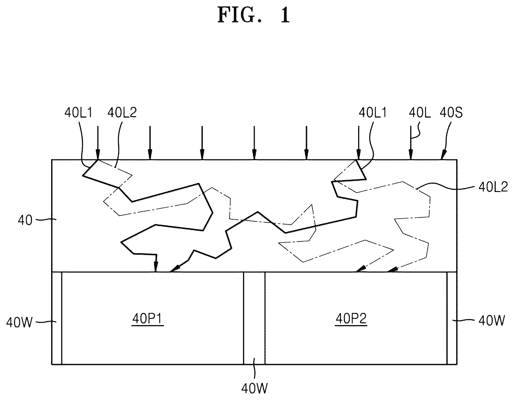
is a cross-sectional view conceptually illustrating a process of color separation and gathering of separated colors occurring in a color routing meta-structure layer applied to an image sensor, according to an example embodiment. A color routing meta-structure layer may be described through the description of .
Referring to , while traveling into the color routing meta-structure layer 40 , the light 40 L incident on the color routing meta-structure layer 40 may be color-separated by the meta-pattern formed on the color-routing meta-structure layer 40 and directed to the pixels (e.g., first pixel 40 P 1 , second pixel 40 P 2 ) corresponding to the separated colors. Consequently, the color routing meta-structure layer 40 may be referred to as a meta-structure layer that may serve as a lens that collects light by color while separating the colors.
In an embodiment, the incident light 40 L incident on the color routing meta-structure layer 40 may include a first light 40 L 1 having a first wavelength, and a second light 40 L 2 having a second wavelength that may be different from the first wavelength. For example, the first light 40 L 1 may be and/or include at least one of red light, green light, and blue light. For another example, the second light 40 L 2 may be and/or include another one of red light, green light, and blue light. For yet another example, the incident light 40 L may further include a third light having a third wavelength different from the first and second wavelengths of first and second lights 40 L 1 and 40 L 2 . In an embodiment, the third light may propagate along a path different from the paths of the first and second lights 40 L 1 and 40 L 2 .
A process in which the first light 40 L 1 propagates into the color routing meta-structure layer 40 at various places of the light incident surface 40 S of the color routing meta-structure layer 40 is described below.
In an embodiment, the first light 40 L 1 may propagate within the color routing meta-structure layer 40 by being scattered by a meta-pattern existing inside the color routing meta-structure layer 40 . Alternatively or additionally, the first light 40 L 1 may be incident to the first pixel 40 P 1 according to a phase change by the meta-pattern. That is, while the departure positions of the first light 40 L 1 at which the first light 40 L 1 is incident on the light incident surface 40 S may be different, the light 40 L 1 may be incident to the first pixel 40 P 1 due to the meta-pattern inside the color routing meta-structure layer 40 .
As a result, since light of the first wavelength is incident (e.g., condensed) to the first pixel 40 P 1 from an area larger than the first pixel 40 P 1 , light efficiency may be improved when compared to related technology.
In an embodiment, the first pixel 40 P 1 may be and/or may include a photoelectric conversion element configured to receive at least one of red light, green light, and blue light. In an optional or additional embodiment, a partition wall 40 W may be arranged between the first and second pixels 40 P 1 and 40 P 2 in order to prevent light current leakage.
The principle of propagation of the second light 40 L 2 in the color routing meta-structure layer 40 may be substantially the same as the principle of propagation of the first light 40 L 1 as described above. However, since the second light 40 L 2 has a different wavelength from the first light 40 L 1 , the second light 40 L 2 may be incident on the second pixel 40 P 2 , even if the second light 40 L 2 departs from a same position as the first light 40 L 1 . For example, when the first pixel 40 P 1 includes a first photoelectric conversion element configured to receive red light, the second pixel 40 P 2 may be and/or include a second photoelectric conversion element configured to receive at least one of green light and blue light.
For another example, when the third light is incident at the same position as the first and second lights 40 L 1 and 40 L 2 , the third light may be incident to a third pixel different from the first and second pixels 40 P 1 and 40 P 2 , since the third light has a different wavelength from the first light and second lights 40 L 1 and 40 L 2 . Alternatively or additionally, the third pixel may be and/or include a photoelectric conversion element configured to receive the other one of green light and blue light.
As shown in , the light 40 L incident on the color routing meta-structure layer 40 may travel in a depth direction from the incident surface 40 S, a travel (e.g., propagation) path of the incident light 40 L may be changed according to a component (e.g., wavelength) of the incident light 40 L. Consequently, substantially similar and/or identical light components of the light 40 L may converge to one place and/or the same pixel. The term “substantially similar light components” may indicate light components that belong to a same color and/or wavelength band such as, but not limited to, a red band, a green band or a blue band.
In an embodiment, the color routing meta-structure layer 40 may include different meta-patterns for each thickness position and/or layer. That is, as the incident light 40 L propagates from the incident surface 40 S of the color routing meta-structure layer 40 (e.g., the upper surface) to the lower surface of the color routing meta-structure layer 40 (e.g., the first and second pixels 40 P 1 and 40 P 2 ), the meta-pattern inside the color routing meta-structure layer 40 may vary. For example, the color routing meta-structure layer 40 may be manufactured to obtain the above result by forming different types of meta-patterns according to the depth of the color routing meta-structure layer 40 . An example of the layer structure of the color routing meta-structure layer 40 is described with reference to to 17 .
is a plan view illustrating an image sensor including a color routing meta-structure layer, according to an example embodiment.
Referring to , an image sensor 100 may include a color routing meta-structure layer that includes a pixel array 120 . The pixel array 120 may include a plurality of unit pixels 130 aligned in a first direction and a second direction. The first and second directions may be perpendicular to each other. For example, the first direction may be a direction parallel to the X axis. For another example, the second direction may be a direction parallel to the Y-axis. That is, the first direction may be referred to as a horizontal direction and the second direction may be referred to as a vertical direction. However, the present disclosure is not limited in this regard. For example, the first direction may be referred to as a vertical direction and the second direction may be referred to in a horizontal direction without departing from the scope of the present disclosure.
illustrates an enlarged plan view of a unit pixel 130 of , according to an embodiment.
For example, the unit pixel 130 may include four pixels (e.g., first pixel PX 1 , second pixel PX 2 , third pixel PX 3 , and fourth pixel PX 4 ) arranged in 2 rows and 2 columns (e.g., 2×2), as shown in .
In an embodiment, the first to fourth pixels PX 1 to PX 4 may be aligned to form a Bayer pattern. However, the present disclosure is not limited in this regard. That is, the first to fourth pixels PX 1 to PX 4 may be arranged in other patterns without deviating from the scope of the present disclosure. For example, the first pixel PX 1 may be a red (R) pixel configured to receive red light, the second and third pixels PX 2 and PX 3 may be green (G) pixels configured to receive green light, and the fourth pixel PX 4 may be a blue (B) pixel configured to receive blue light.
For another example, at least one of the first to fourth pixels PX 1 to PX 4 may be and/or include an infrared (IR) pixel configured to receive infrared rays. Alternatively or additionally, at least one of the first to fourth pixels PX 1 to PX 4 may be and/or include a white (W) pixel configured to receive white light. For another example, the first to fourth pixels PX 1 to PX 4 may be configured to receive at least one of cyan light, magenta light, and yellow light.
is a cross-sectional view of taken in a 4 - 4 ′ direction, according to an embodiment. is a cross-sectional view of taken in a 5 - 5 ′ direction, according to an embodiment.
Referring to together, the unit pixel 130 may include a substrate 140 , a photoelectric conversion layer 150 provided on the substrate 140 , an intermediate layer 160 formed on the photoelectric conversion layer 150 , and a color routing meta-structure layer 170 provided on the intermediate layer 160 .
In an embodiment, the substrate 140 , the photoelectric conversion layer 150 , the intermediate layer 160 , and the color routing meta-structure layer 170 may be sequentially stacked. However, other material layers may be further formed between each layer.
The substrate 140 may include a circuit and/or a circuit unit for driving and controlling a photoelectric conversion element included in the photoelectric conversion layer 150 . In an embodiment, the circuit may include a readout integrated circuit (ROIC). The intermediate layer 160 may be and/or include a material layer that may be transparent to incident light. Alternatively or additionally, the intermediate layer 160 may be and/or include one of the members that provide a spatial distance through which light separated by the color routing meta-structure layer 170 may reach the photoelectric conversion layer 150 . That is, the intermediate layer 160 may be referred to as a spacer. For example, a material constituting the intermediate layer 160 may include, but not be limited to, silicon oxide (SiO 2 ), and the like. In an optional or additional embodiment, the intermediate layer 160 may be omitted between the photoelectric conversion layer 150 and the color routing meta-structure layer 170 , as described with reference to .
In an embodiment, as shown in , the photoelectric conversion layer 150 and the color routing meta-structure layer 170 may directly contact each other.
Referring to to 7 , the photoelectric conversion layer 150 may include photoelectric conversion elements (e.g., first photoelectric conversion element PE 1 , second photoelectric conversion element PE 2 , third photoelectric conversion element PE 3 , and fourth photoelectric conversion element PE 4 ), and a partition wall 180 . In an embodiment the partition wall 180 may be disposed between each of the first to fourth photoelectric conversion elements PE 1 to PE 4 to prevent optical interference. For example, the partition wall 180 may have a structure (e.g., p-deep trench isolation (DTI)) that partially forms a trench between the first to fourth photoelectric conversion elements PE 1 to PE 4 . That is, the partition wall 180 may include a structure including a trench formed between the first to fourth photoelectric conversion elements PE 1 to PE 4 to a depth smaller than the thickness of the photoelectric conversion layer 150 . In an embodiment, the partition wall 180 may have a structure (e.g., full-depth DTI (f-DTI)) forming a trench as a whole between the first to fourth photoelectric conversion elements PE 1 to PE 4 . That is, the partition wall 180 may have a structure including a trench formed between the first to fourth photoelectric conversion elements PE 1 to PE 4 to have a thickness that is substantially similar or the same thickness as the photoelectric conversion layer 150 . In an optional or additional embodiment, the first to fourth photoelectric conversion elements PE 1 to PE 4 may be and/or include photodiodes. However, the present disclosure is not limited in this regard.
The first photoelectric conversion element PE 1 may belong (e.g., correspond) to the first pixel PX 1 , the second photoelectric conversion element PE 2 may belong to the second pixel PX 2 , the third photoelectric conversion element PE 3 may belong to the third pixel PX 3 , and the fourth photoelectric conversion element PE 4 may belong to the fourth pixel PX 4 , respectively.
In an embodiment, the color routing meta-structure layer 170 may have a multi-layer structure, as described with reference to to 18 .
In an embodiment, the color routing meta-structure layer 170 may include meta-pattern areas (e.g., first meta-pattern area MA 1 , second meta-pattern area MA 2 , third meta-pattern area MA 3 , and fourth meta-pattern area MA 4 ).
The first meta-pattern area MA 1 may be an area belonging to the first pixel PX 1 and may correspond to the first photoelectric conversion element PE 1 . The second meta-pattern area MA 2 may be an area belonging to the second pixel PX 2 and may correspond to the second photoelectric conversion element PE 2 . The third meta-pattern area MA 3 may be an area belonging to the third pixel PX 3 and may correspond to the third photoelectric conversion element PE 3 . The fourth meta-pattern area MA 4 may be an area belonging to the fourth pixel PX 4 and may correspond to the fourth photoelectric conversion element PE 4 .
Each of the first to fourth meta-pattern areas MA 1 to MA 4 may include a plurality of meta-patterns 17 MP including a material having a first refractive index and a transparent material layer 17 TM having a second refractive index. The magnitude of the first refractive index may be different from the magnitude of the second refractive index. For example, the first refractive index may be greater than the second refractive index. In an embodiment, the transparent material layer 17 TM may be and/or include a material that may be transparent to incident light and/or a material having a lower refractive index than the refractive index of the plurality of meta-patterns 17 MP. For example, the transparent material layer 17 TM may include, but not be limited to, silicon oxide (SiO 2 ), siloxane-based spin on glass (SOG), silicon nitride (Si 3 N 4 ), aluminum oxide (Al 2 O 3 ), air, and the like.
Each meta-pattern 17 MP may be and/or include a pattern having a size smaller than the wavelength of light incident on the unit pixel 130 . That is, the pattern may be and/or include a nanostructure having a height (e.g., thickness), width, and/or diameter smaller than the wavelength of incident light. For example, the height, width and/or diameter of the nanostructure may be in the range of several nanometers (nm) to hundreds of nanometers. In an embodiment, each meta-pattern 17 MP may be and/or include a nano-post and/or a pattern having a similar shape. However, the present disclosure is not limited in this regard.
For example, the widths and/or diameters of the plurality of meta-patterns 17 MP in the color routing meta-structure layer 170 and/or in each meta-pattern area MA 1 to MA 4 may be substantially similar and/or be the same and/or different from each other. That is, some meta-patterns may have a substantially similar and/or the same width and/or diameter. Alternatively or additionally, other meta-patterns may have different widths and/or diameters.
The three-dimensional shape, width, or diameter of each meta-pattern 17 MP may be constant and/or change in a direction perpendicular to the photoelectric conversion layer 150 (e.g., Z-axis direction), according to example embodiments. For example, when the shape of each meta-pattern 17 MP is a nano post, the nano-post may be a three-dimensional structure in which the diameter of the post may be constant in the vertical direction and/or a three-dimensional structure in which the refractive index changes in the vertical direction.
When the meta-patterns of each layer of the color routing meta-structure layer 170 are different, the refractive indices of each layer may be different, and incident light may be separated by color (e.g., by wavelength) due to this difference. For example, when the shape of each meta-pattern 17 MP is a nano-post, the nano-post may have a three-dimensional structure in which the thickness of the first section and the thickness of the second section between the lower end and the upper end are different from each other. That is, the second section may be one of sections of the nano-post that may be different from the first section, and/or may be different from the rest of the nano-post except for the first section. For another example, the nano-post may have a three-dimensional structure in which a thickness and/or a width continuously changes in the vertical direction. That is, when the three-dimensional shape of each meta-pattern 17 MP is a nano-post, the nano-post may have a three-dimensional structure in which a diameter gradually decreases and/or increases from the bottom to the top and/or from the top to the bottom. Accordingly, the refractive index of the color routing meta-structure layer 170 may vary in the vertical direction from the first position of the horizontal direction (e.g., X-axis direction) according to the provided shape of the meta-pattern 17 MP in each of the meta-pattern areas MA 1 to MA 4 . For example, the first position may be an arbitrary position within each of the meta-pattern areas MA 1 to MA 4 . For another example, the refractive index in the vertical direction at a certain position of the horizontal direction of each of the meta-pattern area MA 1 to MA 4 may not change and/or may not substantially change.
The refractive index characteristic of the color routing meta-structure layer 170 may be applied even when the color routing meta-structure layer 170 has a multi-layer structure, as described with reference to .
In an embodiment, the plurality of meta-patterns 17 MP in each meta-pattern area MA 1 to MA 4 may be formed to form a meta-structure having symmetry on a plane. That is, each of the meta-pattern areas MA 1 to MA 4 on a plane may include a meta-structure having symmetry, which may be implemented by combining a plurality of meta-patterns 17 MP. Consequently, each of the meta-pattern areas MA 1 to MA 4 may be referred to as a meta-structure area and/or as a three-dimensional meta-surface.
The meta-structure between each of the meta-pattern area MA 1 to MA 4 may be different. For example, the meta-structures of the first to fourth meta-pattern areas MA 1 to MA 4 may be different from each other. However, the present disclosure is not limited in this regard.
As used herein, symmetry may refer to the plurality of meta-patterns 17 MP being formed to achieve left-right symmetry, up-down symmetry, diagonal symmetry, and/or rotational symmetry based on the center of the pixel PX 1 including the first meta-pattern area MA 1 on the plane and/or a line passing through the center. As illustrate cross-sections, only left-right symmetry of the first meta-pattern area MA 1 may be seen in . The symmetry of the first meta-pattern area MA 1 may be equally applied to other meta-pattern areas such as second to fourth meta-pattern areas MA 2 to MA 4 .
exemplarily shows the first meta-structure MS 1 formed in the first meta-pattern area MA 1 , according to an embodiment.
Referring to , the first meta-structure MS 1 may be rotationally symmetric with respect to the center of symmetry 6 C 1 . Alternatively or additionally, the first meta-structure MS 1 may have a left-right symmetrical and/or up-down symmetrical structure around the reference lines (e.g., first reference line 8 L 1 and second reference line 8 L 2 ) passing through the center of symmetry 6 C 1 . The center of symmetry 6 C 1 may correspond to the center of the plane of the pixel PX 1 including the first meta-structure MS 1 .
As the first meta-pattern area MA 1 has a three-dimensional meta-structure having symmetry, the light incident on the first meta-pattern area MA 1 may be normally color-separated for each wavelength regardless of the polarization state of the incident light. Alternatively or additionally, a spot of vertically incident light may be located at the center of a pixel. In addition, because the first meta-pattern area MA 1 has a three-dimensional meta-structure having symmetry, the spot of light may move right or left, and/or up or down from the center of the pixel, depending on the incident direction of light. However, the spot of light may not be divided into a plurality of spots and/or the spot may not be located at several places around the center of the pixel at the same time, even when the light is obliquely incident on the first meta-pattern area MA 1 . Accordingly, a signal ratio measured at left and right or at top and bottom of the center of a pixel may be increased, and thus, a phase detection autofocus operation may be possible.
In an embodiment, the meta-structure formed in the second to fourth meta-pattern areas MA 2 to MA 4 may also have a three-dimensional structure having symmetry, and thus, the operation characteristic according to the symmetry of the first meta-pattern area MA 1 may be equally applied to the second to fourth meta-pattern areas MA 2 to MA 4 .
The meta-patterns 17 MP of each area of the second to fourth meta-pattern areas MA 2 to MA 4 of may also be provided to form a three-dimensional meta-structure having symmetry on a plane.
However, as shown in to 11 , the shape on the plane of the three-dimensional meta-structure of each area of the second to fourth meta-pattern areas MA 2 to MA 4 may be different from each other, and may also be different from the shape seen on the plane of the three-dimensional meta-structure formed in the first meta-pattern area MA 1 .
is a plan view exemplarily illustrating a planar shape of a second meta-structure MS 2 formed in a second meta-pattern area MA 2 , according to an embodiment. is a plan view exemplarily illustrating a planar shape of a third meta-structure MS 3 formed in a third meta-pattern area MA 3 , according to an embodiment. is a plan view exemplarily illustrating a planar shape of a fourth meta-structure MS 4 formed in a fourth meta-pattern area MA 4 , according to an embodiment.
Referring to to 11 , the second to fourth meta-structures MS 2 to MS 4 formed in the second to fourth meta-pattern areas MA 2 to MA 4 may have up-down, left-right, and/or rotational symmetry based on respective centers of symmetry (e.g., 7 C 1 , 8 C 1 , and 9 C 1 ) and/or centered on a reference line passing through the respective centers of symmetry (e.g., 7 C 1 , 8 C 1 , and 9 C 1 ). However, the planar form (e.g., distribution form of a plurality of meta-patterns) of each of the meta-structures MS 2 , MS 3 , and MS 4 may different from each other. Alternatively or additionally, the planar form of each of the meta-structures MS 2 , MS 3 , and MS 4 may be different from the planar form of the first meta-structure MS 1 of the first meta-pattern area MA 1 shown in .
As shown in to 11 , the second to fourth meta-structures MS 2 to MS 4 that may be formed in each area of the second to fourth meta-pattern areas MA 2 to MA 4 may also have symmetry. Accordingly, each of the second to fourth meta-pattern areas MA 2 , MA 3 , and MA 4 may have the same color separation and auto-focus characteristics as the first meta-pattern area MA 1 with respect to incident light, as described above. However, considering that the first meta-pattern area MA 1 , the second meta-pattern area MA 2 , and the fourth meta-pattern area MA 4 belong to different pixels, the photoelectric conversion elements into which the colors separated from the first meta-pattern area MA 1 , the second meta-pattern area MA 2 , and the fourth meta-pattern area MA 4 are incident may be different from each other.
For example, the light 4 L 1 incident on the first meta-pattern area MA 1 of may be separated into red light, green light, and blue light due to the meta-structure of the first meta-pattern area MA 1 . In such an example, the red light may be incident on the first photoelectric conversion element PE 1 under the first meta-pattern area MA 1 , the green light may be incident on the second photoelectric conversion element PE 2 belonging to the G pixel, and the blue light may be incident on the fourth photoelectric conversion element PE 4 adjacent to the first photoelectric conversion element PE 1 in a diagonal direction and belonging to the B pixel.
For another example, the light 4 L 1 incident on the second and third meta-pattern areas MA 2 and MA 3 of may also be separated into red light, green light, and blue light. In such an example, the green light may be incident on the second photoelectric conversion element PE 2 under the second meta-pattern area MA 2 and the third photoelectric conversion element PE 3 under the third meta-pattern area MA 3 , the red light may be incident on the first photoelectric conversion element PE 1 belonging to the R pixel, and the blue light may be incident on the fourth photoelectric conversion element PE 4 adjacent in the horizontal and vertical directions.
For another example, the light 4 L 1 incident on the fourth meta-pattern area MA 4 of may also be separated into red light, green light, and blue light. In such an example, the separated blue light may be incident on the fourth photoelectric conversion element PE 4 under the fourth meta-pattern area MA 4 , and the separated red light is incident on the first photoelectric conversion element PE 1 adjacent to the fourth photoelectric conversion element PE 4 in a diagonal direction and belonging to the R pixel, and the separated green light may be incident on the second and/or third photoelectric conversion elements PE 2 and PE 3 adjacent to the fourth photoelectric conversion element PE 4 and belonging to the G pixel.
is a plan view illustrating the above-described exemplary first to fourth meta-structures MS 1 to MS 4 together, according to an embodiment. may be a plan view illustrating the color routing meta-structure layer 170 of the unit pixel 130 as an example. The first to fourth meta-structures MS 1 to MS 4 may correspond to the first to fourth meta-pattern areas MA 1 to MA 4 , respectively, and may be seen as the first to fourth meta-pattern areas MA 1 to MA 4 in the plan view of .
Referring to , reference number CA 1 may denote a meta-structure area including the center area of the color routing meta-structure layer 170 . The meta-structure area CA 1 may not be a physically divided area, but may be an area set for convenience for explanation.
The size and/or area of the meta-structure area CA 1 may be substantially similar and/or the same as the size and/or area of each of the first to fourth meta-structures MS 1 to MS 4 . The meta-structure area CA 1 may be set to include a part of each of the meta-structures MS 1 to MS 4 . For example, on a plane, the meta-structure area CA 1 may include one fourth (e.g., ¼) of each of the first to fourth meta-structures MS 1 to MS 4 . For example, the meta-structure area CA 1 may include the fourth quadrant of the first meta-structure MS 1 , the third quadrant of the second meta-structure MS 2 , the first quadrant of the third meta-structure MS 3 , and the second quadrant of the fourth meta-structure MS 4 .
Since the meta-structure included in the meta-structure area CA 1 may be composed of parts of each of the first to fourth meta-structures MS 1 to MS 4 having different meta-structures, the meta-structure area CA 1 may not have symmetry. However, the present disclosure is not limited in this regard. For example, in an embodiment, the meta-structure area CA 1 may have symmetry.
To improve autofocus performance, the first to fourth meta-structures MS 1 to MS 4 of the color routing meta-structure layer 170 may each have their own symmetry, and in the meta-structure area CA 1 , the first to fourth meta-structures MS 1 to MS 4 may be freely designed so that each of the first to fourth meta-structures MS 1 to MS 4 has the symmetry. Accordingly, the meta-structure area CA 1 may be referred to as a free design area in which a meta-structure is freely designed.
For example, a meta-structure may be formed in an arbitrary shape in a portion belonging to each of the meta-structures MS 1 to MS 4 in the meta-structure area CA 1 . However, meta-structures may be formed in different shapes in portions belonging to each of the meta-structure MS 1 to MS 4 in the meta-structure area CA 1 . For example, an arbitrary type of meta-structure (hereinafter referred to as a first seed meta-structure and/or a first unit meta-structure) may be formed in a portion of the meta-structure area CA 1 belonging to the first meta-structure MS 1 , an arbitrary type of meta-structure (hereinafter referred to as a second seed meta-structure and/or a second unit meta-structure) may be formed in a portion of the meta-structure area CA 1 belonging to the second meta-structure MS 2 , an arbitrary type of meta-structure (hereinafter referred to as a third seed meta-structure and/or a third unit meta-structure) may be formed in a portion of the meta-structure area CA 1 belonging to the third meta-structure MS 3 , and an arbitrary type of meta-structure (hereinafter referred to as a fourth seed meta-structure and/or a fourth unit meta-structure) may also be formed in a portion of the meta-structure area CA 1 belonging to the fourth meta-structure MS 4 . The first to fourth seed meta-structures may be different meta-structures from each other, and many meta-patterns may be provided to have different shapes from each other on a plane.
In an embodiment, the first seed meta-structure may correspond to the meta-structure formed in the fourth quadrant of the first meta-structure MS 1 . In order to form the first meta-structure MS 1 , the first seed meta-structure may be repeated so that the first meta-structure MS 1 may be left-right symmetrical about the first reference line 8 L 1 in . Alternatively or additionally, the repeated result may be repeated again so as to be up-down symmetric about the second reference line 8 L 2 . For example, in order to form the first meta-structure MS 1 , the first seed meta-structure may be repeated so as to be up-down symmetrical around the second reference line 8 L 2 . Alternatively or additionally, the repeated result may be repeated again so as to be left-right symmetric about the first reference line 8 L 1 .
In an embodiment, the second seed meta-structure may correspond to the meta-structure formed in the third quadrant of the second meta-structure MS 2 . In order to form the second meta-structure MS 2 , the second seed meta-structure may be repeated so that the second meta-structure MS 2 may be left-right symmetrical about the horizontal and/or vertical reference lines 9 L 1 and 9 L 2 in passing through the center of symmetry 7 C 1 . Alternatively or additionally, the repeated result may be repeated again so as to be up-down symmetrical about the horizontal and/or vertical reference lines 9 L 1 and 9 L 2 .
In an embodiment, the third seed meta-structure may correspond to the meta-structure formed in the first quadrant of the third meta-structure MS 3 . In order to form the third meta-structure MS 3 , the third seed meta-structure may be repeated so that the third meta-structure MS 3 may be left-right symmetrical about the horizontal and/or vertical reference lines 10 L 1 and 10 L 2 in passing through the center of symmetry 8 C 1 . Alternatively or additionally, the repeated result may be repeated so as to be up-down symmetrical about the horizontal and/or vertical reference lines 10 L 1 and 10 L 2 .
In an embodiment, the fourth seed meta-structure may correspond to the meta-structure formed in the second quadrant of the fourth meta-structure MS 4 . In order to form the fourth meta-structure MS 4 , the fourth seed meta-structure may be repeated so that the fourth meta-structure MS 4 may be left-right symmetrical about the horizontal and/or vertical reference lines 11 L 1 and 11 L 2 in passing through the center of symmetry 9 C 1 . Alternatively or additionally, the repeated result may be repeated so as to be up-down symmetrical about the horizontal and/or vertical reference lines 11 L 1 and 11 L 2 .
As such, since the first to fourth meta-structures MS 1 to MS 4 may be repetitions of the first to fourth seed meta-structures having different meta-structures, each of the meta-structures MS 1 to MS 4 may have independent symmetry. That is, each of the meta-structures MS 1 to MS 4 may include meta-patterns formed to have independent symmetry.
Since the meta-structures may be created by combining a plurality of meta-patterns, meta-patterns having various forms may be distributed in various forms in the meta-structure area CAL Accordingly, the first to fourth meta-structures MS 1 to MS 4 may be modified to have various meta-structures different from each other.
The color routing meta-structure layer 170 may be formed through processes of setting an objective function (e.g., model) to achieve set color separation and/or auto focus and/or to obtain the desired optical properties. That is, the color routing meta-structure layer 170 may be formed from a meta-structure that may satisfy the objective function in the meta-structure area CA 1 while keeping the independent symmetry of each of the first to fourth meta-structures MS 1 to MS 4 . The process of forming a meta-structure that may satisfy the objective function may include a process of inputting information on various meta-structures into the objective function. This process may be repeated until a meta-structure satisfying the objective function is found. Each time this process is repeated, the information input to the objective function may change. For example, the information on the meta-structure may include the width, diameter, pitch, material, refractive index, and/or dimensions defining the shape of the meta-pattern constituting the meta-structure. However, the present disclosure may not be limited in this regard. For example, one of the optical characteristics may include a characteristic that the same optical efficiency may be obtained in each pixel regardless of the polarization of the incident light. Consequently, in the case of the image sensor 100 provided with the exemplary color routing meta-structure layer 170 , the same light efficiency may be obtained in each pixel regardless of the polarization state of incident light, as described with reference to .
shows an example embodiment of a color routing meta-structure layer 1070 implemented through simulation to satisfy the above objective function, according to an embodiment.
Referring to , the color routing meta-structure layer 1070 may include four meta-structures (e.g., first meta-structure 10 M 1 , second meta-structure 10 M 2 , third meta-structure 10 M 3 , and fourth meta-structure 10 M 4 ). Each of the first to fourth meta-structures 10 M 1 to 10 M 4 may have an independent symmetry. However, there may be no symmetry between each of the first to fourth meta-structures 10 M 1 to 10 M 4 . Alternatively or additionally, the meta-structure of the central area CA 2 corresponding to the meta-structure area CA 1 of the color routing meta-structure layer 170 of may include respective portions of the first to fourth meta-structures 10 M 1 to 10 M 4 , however, the first to fourth meta-structures 10 M 1 to 10 M 4 may not have symmetry with each other.
For example, the central area CA 2 of the color routing meta-structure layer 1070 may be an area where the meta-structure is freely designed so that the color routing meta-structure layer 1070 satisfies the objective function. Each of the first to fourth meta-structures 10 M 1 to 10 M 4 may be designed to have symmetry based on a part belonging to each of the first to fourth meta-structures 10 M 1 to 10 M 4 in the meta-structure designed in the central area CA 2 . Conversely, each of the first to fourth meta-structures 10 M 1 to 10 M 4 may have independent symmetry while satisfying the objective function, however, the first to fourth meta-structures 10 M 1 to 10 M 4 may be formed so as not to have symmetry between each of the first to fourth meta-structures 10 M 1 to 10 M 4 , and as such, a meta-structure that may not naturally have symmetry may be formed in the central area CA 2 .
In an embodiment, the color routing meta-structure layer 170 of to 7 may be and/or include a single layer of a three-dimensional structure. In an optional or additional embodiment, as shown in , the color routing meta-structure layer 170 may include color routing meta-structure layers (e.g., first color routing meta-structure layer 170 A, second color routing meta-structure layer 170 B, third color routing meta-structure layer 170 C, fourth color routing meta-structure layer 170 D, and fifth color routing meta-structure layer 170 E) that may be sequentially stacked.
It is to be understood that the layer structure of the color routing meta-structure layer 170 of is exemplary, and that the color routing meta-structure layer 170 may include fewer layers (e.g., less than five (5)) and/or additional layers (e.g., more than five (5)). For example, the color routing meta-structure layer 170 may include only two layers among the first to fifth color routing meta-structure layers 170 A to 170 E.
Planar areas of the first to fifth color routing meta-structure layers 170 A to 170 E may be substantially similar and/or be the same as each other. Alternatively or additionally, the first to fifth color routing meta-structure layers 170 A to 170 E may have different meta-structures. Accordingly, the meta-structures formed in the first to fifth color routing meta-structure layers 170 A to 170 E may not have a symmetrical relationship with each other. That is, there may be no symmetric relationship between the meta-structures formed in the first to fifth color routing meta-structure layers 170 A to 170 E.
In the first to fifth color routing meta-structure layers 170 A to 170 E, the meta-structure of each layer may be provided in a form capable of achieving color routing of incident light as described with reference to .
In embodiments in which the color routing meta-structure layer 170 includes 2 layers, 3 layers, and/or 4 layers, the meta-structure of each layer may be provided in a form capable of achieving color routing of incident light as described with reference to .
is an exploded perspective three-dimensional (3D) view illustrating the color routing meta-structure layer 170 including the first to fifth color routing meta-structure layers 170 A to 170 E.
As shown in , each of the first to fifth color routing meta-structure layers 170 A to 170 E may include first to fourth meta-structure areas 17 A 1 to 17 A 4 in which meta-structures are formed. For convenience of illustration, the meta-structures (e.g., meta-patterns) are not shown in the first to fourth meta-structure areas 17 A 1 to 17 A 4 in .
In each layer of the first to fifth color routing meta-structure layers 170 A to 170 E, the meta-structures formed in the first to fourth meta-structure areas 17 A 1 to 17 A 4 may be different from each other. For example, the meta-structures formed in the first meta-structure areas 17 A 1 of the first to fifth color routing meta-structure layers 170 A to 170 E may be different from each other. For another example, the meta-structures formed in the second meta-structure areas 17 A 2 of the first to fifth color routing meta-structure layers 170 A to 170 E may be different from each other. Alternatively or additionally, the meta-structures formed in the third meta-structure areas 17 A 3 of the first to fifth color routing meta-structure layers 170 A to 170 E may be different from each other. For another example, the meta-structures formed in the fourth meta-structure areas 17 A 4 of the first to fifth color routing meta-structure layers 170 A to 170 E may be different from each other. That is, when viewing on a planar view, the result of vertically overlapping the meta-structures formed in the first meta-structure areas 17 A 1 of the first to fifth color routing meta-structure layers 170 A to 170 E may be and/or correspond to the first meta-structure MS 1 of the color routing meta-structure layer 170 of .
is a cross-sectional view illustrating the first color routing meta-structure layer 170 A as an example. is a cross-sectional view perpendicular to the Y-axis, and may be a cross section of the first and second meta-structure areas 17 A 1 and 17 A 2 or the third and fourth meta-structure areas 17 A 3 and 17 A 4 cut in a direction parallel to a plane formed by the X-axis and the Z-axis (e.g., a X-Z plane).
Referring to , the first color routing meta-structure layer 170 A may include a substrate 1310 and a meta-surface 1320 formed on the substrate 1310 . The meta-surface 1320 may also be referred to as a meta-surface layer. The substrate 1310 may be and/or include a substrate that may be transparent to incident light and/or may include a substrate formed of a material that may not absorb and/or may not substantially absorb incident light. For example, the substrate 1310 may be a related substrate on which a meta-surface may be formed. In an embodiment, the substrate 1310 may correspond to the intermediate layer (e.g., spacer) 160 described with reference to . For example, the substrate 1310 may correspond to the photoelectric conversion layer 150 shown in and/or include the photoelectric conversion layer 150 .
The meta-surface 1320 may include meta-patterns (e.g., first meta-pattern 13 A, second meta-pattern 13 B, third meta-pattern 13 C, fourth meta-pattern 13 D, fifth meta-pattern 13 E, sixth meta-pattern 13 F, and seventh meta-pattern 13 G) and a protective layer 1330 having different refractive indices from each other. A dimension (e.g., height, width, thickness, pitch) of each of the meta-patterns 13 A to 13 G may be smaller than the wavelength of the incident light. For example, the height and/or lateral width of each of the meta-patterns 13 A to 13 G may be smaller than the wavelength of the incident light. For another example, the interval and/or pitch of each of the meta-patterns 13 A to 13 G may be smaller than the wavelength of the incident light. The plurality of meta-patterns 13 A, 13 B, and 13 C included in the third meta-structure area 17 A 3 may be aligned so as to be left-right symmetrical. Alternatively or additionally, the plurality of meta-patterns 13 D and 13 E included in the fourth meta-structure area 17 A 4 may be arranged so as to be left-right symmetrical. However, the number and/or arrangement of the plurality of meta-patterns 13 A, 13 B, and 13 C included in the third meta-structure area 17 A 3 may be different from the number and/or arrangement of the plurality of meta-patterns 13 D and 13 E included in the fourth meta-structure area 17 A 4 . For example, the number of meta-patterns 13 A to 13 C included in the third meta-structure area 17 A 3 and the number of meta-patterns 13 D to 13 G included in the fourth meta-structure area 17 A 4 may be the same, however, the arrangement of the meta-patterns 13 A to 13 C may be different from the arrangement of the meta-patterns 13 D to 13 G. For example, the third and fourth meta-structure areas 17 A 3 and 17 A 4 may include the same number of meta-patterns, and in each of the meta-structure areas 17 A 3 and 17 A 4 , the meta-patterns may be arranged symmetrically, however, the arrangement of meta-patterns in the third meta-structure area 17 A 3 may be different from the arrangement of meta-patterns in the fourth meta-structure area 17 A 4 . These characteristics related to the meta-patterns 13 A to 13 G between the third and fourth meta-structure areas 17 A 3 and 17 A 4 may be applied between the first and second meta-structure areas 17 A 1 and 17 A 2 , and/or may also be applied between the first and third meta-structure areas 17 A 1 and 17 A 3 and between the second and fourth meta-structure areas 17 A 2 and 17 A 4 . A portion of the plurality of meta-patterns 13 A to 13 G may be covered with the protective layer 1330 . The top surface of some of the plurality of meta-patterns 13 A to 13 G may be at the same height and/or substantially the same height as the top surface of the protective layer 1330 , such that the same plane as the upper surface of the protective layer 1330 may be formed. An upper surface of the protective layer 1330 may be parallel to a surface of the substrate 1310 on which the plurality of meta-patterns 13 A to 13 G may be formed, and/or may be flat.
In an embodiment, the protective layer 1330 may include a material that may have a refractive index smaller than a refractive index of the plurality of meta-patterns 13 A to 13 G and may be transparent to incident light. For example, the material of the protective layer 1330 may be the same as that of the transparent material layer 17 TM described in , but may be different from each other. The meta-patterns 13 A to 13 G may include a material such as, but not limited to, titanium oxide (TiO 2 ).
is a cross-sectional view illustrating the second color routing meta-structure layer 170 B of as an example, according to an embodiment.
Referring to , the second color routing meta-structure layer 170 B may include a meta-surface 1420 formed on the first color routing meta-structure layer 170 A illustrated in . In an embodiment, the first color routing meta-structure layer 170 A and the meta-surface 1420 may be in direct contact with each other. For example, a member (e.g., a material layer) transparent to the incident light may be provided between the first color routing meta-structure layer 170 A and the meta-surface 1420 .
The plurality of meta-patterns (e.g., first meta-pattern 14 A, second meta-pattern 14 B, third meta-pattern 14 C, fourth meta-pattern 14 D, fifth meta-pattern 14 E, sixth meta-pattern 14 F, and seventh meta-pattern 14 G) included in the meta-surface 1420 of the second color routing meta-structure layer 170 B may be aligned with left-right symmetry in the third meta-structure area 17 A 3 . Alternatively or additionally, the plurality of meta-patterns may be aligned with left-right symmetry in the fourth meta-structure area 17 A 4 . However, the alignment form (e.g., meta-structure) of the meta-patterns 14 A to 14 C included in the third meta-structure area 17 A 3 may be different from the alignment form (e.g., meta-structure) of the meta-patterns 14 D to 14 G included in the fourth meta-structure area 17 A 4 .
Comparing , the alignment form (e.g., meta-structure) of the meta-patterns 13 A to 13 C included in the third meta-structure area 17 A 3 of the first color routing meta-structure layer 170 A may be different from the alignment form (e.g., meta-structure) of the meta-patterns 14 A to 14 C included in the third meta-structure area 17 A 3 of the second color routing meta-structure layer 170 B. The alignment form (e.g., meta-structure) of the meta-patterns 13 D to 13 G included in the fourth meta-structure area 17 A 4 of the first color routing meta-structure layer 170 A may be different from the alignment form (e.g., meta-structure) of the meta-patterns 14 D to 14 G included in the fourth meta-structure area 17 A 4 of the second color routing meta-structure layer 170 B.
In an embodiment, each of the third to fifth color routing meta-structure layers 170 C to 170 E of may include a meta-surface, in a manner similar to the second color routing meta-structure layer 170 B including the meta-surface 1420 . However, in a manner similar to the meta-structure characteristics of the meta-surfaces 1320 and 1420 of the first and second color routing meta-structure layers 170 A and 170 B being different from each other, the meta-structure characteristics of the meta-surfaces of the third to fifth color routing meta-structure layers 170 C to 170 E may be different from each other. Alternatively or additionally, the meta-structure characteristics of the meta-surfaces of the third to fifth color routing meta-structure layers 170 C to 170 E may be different from the meta-structural characteristics of the meta-surfaces 1320 and 1420 of the first and second color routing meta-structure layers 170 A and 170 B.
As described above, since the meta-structures between the vertically stacked first to fifth color routing meta-structure layers 170 A to 170 E may be different from each other, even when the constituent materials of each layer of the first to fifth color routing meta-structure layers 170 A to 170 E may be the same, the refractive index in the vertical direction of the multi-layered color routing meta-structure layer 170 may be different. However, the refractive index in the vertical direction may be constant at a certain location where the meta-structures between the first to fifth color routing meta-structure layers 170 A to 170 E partially overlap. When the refractive index in the vertical direction is changed, the refractive index change may be continuous and/or discontinuous depending on the position.
For example, constituent materials of the first to fifth color routing meta-structure layers 170 A to 170 E may be different for each layer. Taking the first color routing meta-structure layer 170 A and the second color routing meta-structure layer 170 B as an example, the first color routing meta-structure layer 170 A may include a first material and a second material having different refractive indices from each other, and the second color routing meta-structure layer 170 B may include a third material and a fourth material having different refractive indices from each other. In such an example, at least one of the first material and the second material and at least one of the third material and the fourth material may be the same material. As a result, when the constituent materials of each layer of the first to fifth color routing meta-structure layers 170 A to 170 E are different from each other, even when the meta-structure between the first to fifth color routing meta-structure layers 170 A- 170 E are not only different but also the same, refractive indices in the vertical direction may be different.
In an embodiment, layer constituent materials of some of the first to fifth color routing meta-structure layers 170 A to 170 E may be different from those of other layers. For example, the layer constituent materials of the first and second color routing meta-structure layers 170 A and 170 B may be the same each other, but may be different from those of the third to fifth color routing meta-structure layers 170 C to 170 E. In such an example, the layer constituent materials of the third to fifth color routing meta-structure layers 170 C to 170 E may be the same and/or different from each other. As a result, when the layer constituent materials of some layers of the first to fifth color routing meta-structure layers 170 A to 170 E are different from those of the other layers, since the first to fifth color routing meta-structure layers 170 A to 170 E have different meta-structures from each other, the refractive index in the vertical direction of the color routing meta-structure layer 170 may vary, and the refractive index in the vertical direction may be constant only at a certain location.
is an example of a case in which the color routing meta-structure layer 1070 implemented by the simulation of is multi-layered, according to an embodiment. Referring to , first to fifth color routing meta-structure layers (a) to (e) constituting the color routing meta-structure layer 1070 are shown. The first to fifth color routing meta-structure layers (a) to (e) may be formed with simulation so as to form the color routing meta-structure layer 1070 by sequentially stacking the first to fifth color routing meta-structure layers (a) to (e).
Continuing to refer to , it may be seen that each of the first to fifth color routing meta-structure layers (a) to (e) has a meta-structure having symmetry, but the meta-structural characteristics of each of the first to fifth color routing meta-structure layers (a) to (e) are different from each other. Taking the first and second color routing meta-structure layers (a) and (b) as an example, the first to fourth meta-structures 15 A 1 to 15 A 4 of the first color routing meta-structure layer (a) and the first to fourth meta-structures 15 B 1 to 15 B 4 of the second color routing meta-structure layer (b) are located at positions corresponding to the first to fourth meta-structures 10 M 1 to 10 M 4 of the color routing meta-structure layer 1070 of , and each independently has symmetry. However, the first to fourth meta-structures 15 A 1 to 15 A 4 of the first color routing meta-structure layer (a) are different from each other, and the first to fourth meta-structures 15 B 1 to 15 B 4 of the second color routing meta-structure layer (b) are also different from each other. The meta-structure of the first color routing meta-structure layer (a) is also different from the meta-structure of the entire second color routing meta-structure layer (b). Reference number CA 3 in the first color routing meta-structure layer (a) denotes a central area corresponding to the central area CA 2 of the color routing meta-structure layer 1070 of . Reference numbers SC 1 to SC 4 denote centers of symmetry, and may correspond to pixel centers on a plane.
to 21 show simulation results performed to check polarization characteristics or polarization dependence of the image sensor 100 including the color routing meta-structure layer, according to an example embodiment. In such a simulation, the color routing meta-structure layer may be set to be the color routing meta-structure layer 1070 of .
( a ) shows a simulation result when a first incident light having a wavelength of 450 nm and linearly polarized in a first direction (e.g., +45° direction) is incident on the color routing meta-structure layer. ( b ) shows a simulation result when a second incident light having a wavelength of 450 nm and linearly polarized in a second direction perpendicular to the first direction (e.g., +135° direction) is incident to the color routing meta-structure layer. In (a) and (b) of , double-headed arrows indicate the direction of linear polarization of incident light.
Comparing (a) and (b) of , both the first and second incident light may be received in the central area of a pixel receiving blue light B. The spot (e.g., brightest part) of the first incident light may be concentrated on the center of a corresponding pixel and may have vertical and horizontal symmetry (e.g., left-right symmetry and up-down symmetry). In a similar manner to the spot of the first incident light in (a), the spot of the second incident light in (b) may be concentrated on the center of the corresponding pixel and may have vertical and horizontal symmetry.
The results of may show that the image sensor 100 may not exhibit linear polarization dependence on incident light in the 450 nm band. That is, the results of may suggest that when incident light in the blue light band is incident on the image sensor 100 , light efficiency of the image sensor 100 may not be affected by polarization characteristics of the incident light.
( a ) shows a simulation result when the third incident light having a wavelength of 550 nm and linearly polarized in the first direction is incident on the color routing meta-structure layer. ( b ) shows a simulation result when the fourth incident light having a wavelength of 550 nm and linearly polarized in the second direction is incident to the color routing meta-structure layer.
Comparing (a) and (b) of , both the third and fourth incident lights may be received by pixels receiving green light G, and the spot (e.g., brightest part) of the third incident light in a corresponding pixel may be located at the center of the pixel, may have symmetry, and may be limitedly spread in a given direction. The spot of the fourth incident light may have substantially the same distribution shape and symmetry as the spot of the third incident light and may be limitedly spread. However, the spread direction of the spot of the fourth incident light may be perpendicular to the spread direction of the spot of the third incident light.
Although the spots of the third and fourth incident light may be restrictedly spread and the spreading directions may be perpendicular to each other, since the spots of the third and fourth incident light may be formed at the center of the pixel, and the spread area of the spot may be gathered at the center of the pixel, both the third and fourth incident light spots may be considered to be formed at the center of a pixel.
The results of may show that the image sensor 100 may not exhibit linear polarization dependence even for incident light in a 550 nm band. That is, the results of may suggest that even when incident light in the green light band is incident on the image sensor 100 , the optical efficiency of the image sensor 100 may not be affected by the polarization characteristics of the incident light.
( a ) shows a simulation result when the fifth incident light having a wavelength of 650 nm and linearly polarized in the first direction is incident on the color routing meta-structure layer. ( b ) shows a simulation result when the sixth incident light having a wavelength of 650 nm and linearly polarized in the second direction is incident to the color routing meta-structure layer.
Comparing (a) and (b) of , both the fifth and sixth incident lights may be received in the central area of a pixel receiving red light R, and the spot of the fifth incident light may be concentrated on the center of a corresponding pixel and may have vertical and horizontal symmetry. The sixth incident light may have substantially similar and/or the same spot characteristics and symmetry as those of the fifth incident light.
The results of may show that the image sensor 100 may not exhibit linear polarization dependence even for incident light in a 650 nm band. That is, the results of may suggest that even when incident light in the red light band is incident on the image sensor 100 , the optical efficiency of the image sensor 100 may not be affected by the polarization characteristics of the incident light.
The results of to 21 may suggest that the optical efficiency of the image sensor 100 provided with the exemplary color routing meta-structure layer may not be affected by the polarization characteristics of incident light in the visible light band.
The simulation results of to 21 illustrate a case where the light may be perpendicular to the pixel, that is, the incident angle may be 0° and/or may be substantially the same as 0°. “Substantially the same as 0°” may refer to an incident angle where the incident angle may not be equal to 0°, but the size and/or position of the light spot may not change and/or may not show a significant difference from when the incident angle is equal to 0°.
In the simulation used to obtain the results of to 21 , when the angle of incidence of light incident on a pixel is greater than 0°, that is, when light is obliquely incident, the spot of light formed on the pixel may be different from that of to 21 , and an R pixel is described with reference to , as an example.
shows simulation results showing a positional movement of a light spot in an R pixel when light is incident vertically and/or obliquely to an image sensor including a color separation meta-structure, according to an example embodiment. In the simulation used to obtain the simulation results, a light having a wavelength of 650 nm belonging to the red light band was used as the incident light, and the simulation was performed at incident angles of 0°, +5°, +10°, and −10°.
Referring to , image (a) corresponds to the simulation result when the incident angle is 0°, image (b) corresponds to the simulation result when the incident angle is +5°, image (c) corresponds to the simulation result when the incident angle is +10°, and image (d) corresponds to the simulation result when the incident angle is −10°.
As shown in , a virtual horizontal reference line 23 L 1 is introduced to aid in understanding of the description.
Continuing to refer to , when the incident angle is 0°, the spot of light may be located at the center of the R pixel. The virtual horizontal reference line 23 L 1 may be considered to pass through the center of the spot of light when the incident angle is 0°. When the incident angle of light is +5°, the spot of light may be slightly moved below the virtual horizontal reference line 23 L 1 . That is, the center of the spot of light may be shifted slightly downward from the center of the R pixel. The spot of light may not be divided and may maintain a single spot state.
When the incident angle of light is +10°, the center of the light spot may be moved more downward from the virtual horizontal reference line 23 L 1 compared to the incident angle of light being +5°. That is, the center of the spot of light may be moved more downward from the center of the pixel than when the incident light is +5°. The spot of light may not be divided, and may maintain a single spot state.
When the angle of incidence of light is −10°, the spot of light may be moved in a direction opposite to that when the angle of incidence of light is +10°. That is, the center of the spot of light may be moved above the virtual horizontal reference line 23 L 1 . The spot of light may not be divided and may maintain a single spot state.
When light is incident vertically as shown in image (a) of , the light spot is located at the center of the pixel. Accordingly, the upper/lower signal ratio with respect to the center of the pixel may be equal to one (1) and/or be approximately equal to one (1). When light is obliquely incident (e.g., images (b), (c), (d) of ), the light spot may move downward and/or upward from the center of the pixel depending on the incident direction while maintaining a single spot state. Accordingly, when light is obliquely incident, a difference between an optical signal measured at an upper side (e.g., lower side) of the center of a pixel and an optical signal measured at the lower side (e.g., the upper side) of the center of the pixel may increase. That is, the upper and lower signal ratios with respect to the center of the pixel may be increased. These results suggest that phase detection autofocus operation is possible.
In the first to fifth color routing meta-structure layers (a) to (e) shown in , each layer may include two areas respectively corresponding to two G pixels, and the meta-structure may be formed in two areas that may have independent symmetry, and there may be no symmetry between the meta-structures in the two areas. However, in another example, the meta-structures of the two areas may be formed to have symmetry with each other.
For example, as shown in , areas (e.g. first red area 23 A 1 , second red area 23 B 1 , third red area 23 C 1 , fourth red area 23 D 1 , and fifth red area 23 E 1 ) corresponding to R pixels and areas (e.g., first blue area 23 A 4 , second blue area 23 B 4 , third blue area 23 C 4 , fourth blue area 23 D 4 , and fifth blue area 23 E 4 ) corresponding to B pixels in each of the color routing meta-structure layers (a) to (e) may include meta-structures having independent symmetry, and two areas (e.g., first green area 23 A 2 , second green area 23 A 3 , third green area 23 B 2 , fourth green area 23 B 3 , fifth green area 23 C 2 , sixth green area 23 C 3 , seventh green area 23 D 2 , eighth green area 23 D 3 , ninth green area 23 E 2 , and tenth green area 23 E3) corresponding to the G pixel may also include meta-structures having independent symmetry. However, there may be symmetry between the meta-structures formed in the two areas 23 A 2 to 23 E 3 corresponding to the G pixel. Taking the first color routing meta-structure layer (a) as an example, the meta-structures formed in the second and third areas 23 A 2 and 23 A 3 corresponding to the G pixels in the first color routing meta-structure layer (a) may be provided so as to be symmetrical to each other with respect to the diagonal line DL 1 passing through the centers of symmetry SC 5 and SC 8 of the first and fourth areas 23 A 1 and 23 A 4 and the contact point between the second and third areas 23 A 2 and 23 A 3 .
To secure this symmetry between the meta-structures formed in the second and third areas 23 A 2 and 23 A 3 , when forming the first color routing meta-structure layer (a) or setting conditions for formation, the area CA 4 in which the meta-structure may be freely designed may be limited differently from the central area CA 3 shown in ( a ) . For example, the area CA 4 in which the meta-structure may be freely designed in the first color routing meta-structure layer (a) may correspond to half of the central area CA 3 shown in ( a ) , and may be an area that does not include the second area 23 A 2 and includes one eighth (e.g., ⅛) of the first area 23 A 1 , one fourth (e.g., ¼) of the third area 23 A 3 , and one eighth of the fourth area 23 A 4 . In an embodiment, the area CA 4 may be limited in a similar manner to an area CA 4 ′ indicated with a dotted line. The area CA 4 ′ limited by the dotted line may include the third area 23 A 3 .
As shown in , reference numbers SC 5 to SC 8 may denote centers of symmetry. The three corners of the free design area CA 4 or CA 4 ′ may be located at the centers SC 5 , SC 7 , and SC 8 of symmetry of the first, third and fourth areas 23 A 1 , 23 A 3 , and 23 A 4 , and/or may be located at the centers SC 5 , SC 6 , and SC 8 of symmetry of the first, second, and fourth areas 23 A 1 , 23 A 2 , and 23 A 4 .
Areas in which the meta-structure may be freely designed in the color routing meta-structure layer may be set in various shapes other than the aforementioned square (e.g., CA 1 in , CA 2 in , and CA 3 in ) and/or triangle (e.g., CA 4 and CA 4 ′ in ).
For example, when a pixel layer includes a red pixel, a blue pixel, two green pixels that are arranged in a two-by-two matrix form, the color routing meta-structure layer may include symmetrical meta-structures which are provided directly above the two green pixels and are arranged in a diagonal direction, and non-symmetrical meta-structures that have random and asymmetrical structures, and are provided in a remaining area of the color routing meta-structure layer.
exemplarily shows an example of one or more free design areas, according to an embodiment.
Referring to , the free design area CA 5 of the color routing meta-structure layer 280 may be set to be a rectangle. For example, one side of the rectangle may be a diagonal line DL 2 passing through centers of symmetry SC 9 and SC 12 of the first and fourth areas 24 A 1 and 24 A 4 . In such an example, the free design area CA 5 may have a rectangular shape inclined at the same angle as the diagonal line DL 2 . One side of the rectangular shape may be on the diagonal line DL 2 . The rectangular shape may be set to include one fourth of the first area 24 A 1 (e.g., a triangular area connecting vertices of the upper and lower ends of right side of the first area 24 A 1 to the center of symmetry SC 9 ), half of the second area 24 A 2 (e.g., an area between the diagonal line DL 2 and the imaginary line passing through the center of symmetry SC 10 and parallel to the diagonal line DL 2 ), and one fourth of the fourth area 24 A 4 (e.g., a triangular area connecting the upper left and right vertices of the fourth area 24 A 4 to the center of symmetry SC 12 ). Alternatively or additionally, the free design area CA 5 may not include the third area 24 A 3 of the color routing meta-structure layer 280 .
In order to form the meta-structure 24 M 1 of the first area 24 A 1 , the seed meta-structure formed in the one fourth of the first area 24 A 1 included in the rectangular shape CA 5 may be repeated so that the first area 24 A 1 may be symmetrical with respect to the diagonal line DL 2 . Alternatively or additionally, the repeated result may be repeated again so as to be symmetrical with respect to the +45° diagonal line (e.g., the diagonal line of the first area 24 A 1 passing through the center of symmetry SC 9 and perpendicular to the diagonal line DL 2 ). For example, in order to form the meta-structure 24 M 1 of the first area 24 A 1 , the seed meta-structure formed in the one fourth of the first area 24 A 1 included in the rectangular shape CA 5 may be repeated so that the first area 24 A 1 may be symmetrical with respect to the +45° diagonal line, and/or the repeated result may be repeated again so as to be symmetrical with respect to the diagonal line DL 2 .
Accordingly, the meta-structure 24 M 1 of the first area 24 A 1 may be symmetrical with respect to the +45° diagonal line and/or may be symmetrical with respect to the −45° diagonal line, that is, the diagonal line DL 2 .
In order to form the meta-structure 24 M 2 of the second area 24 A 2 , the seed meta-structure formed in the half area of the second area 24 A 2 included in the rectangular shape CA 5 may be repeated so that the second area 24 A 2 may be symmetrical with respect to the virtual line passing through the center of symmetry SC 10 . Accordingly, the meta-structure 24 M 2 of the second area 24 A 2 may be symmetrical with respect to the virtual line parallel to the diagonal line DL 2 , that is, the −45° diagonal line of the second area 24 A 2 .
The meta-structure 24 M 3 of the third area 24 A 3 may formed in a substantially similar and/or the same manner as the meta-structure 24 M 2 of the second area 24 A 2 being further formed on the opposite side of the diagonal line DL 2 so as to be symmetric with respect to the diagonal line DL 2 . Therefore, the meta-structure 24 M 3 of the third area 24 A 3 may be symmetric about the −45° diagonal line of the third area 24 A 3 passing through the center of symmetry SC 11 of the third area 24 A 3 and parallel to the diagonal line DL 2 .
The meta-structure 24 M 4 of the fourth area 24 A 4 may be a result from the seed meta-structure formed in the one fourth of the fourth area 24 A 4 being repeatedly formed on the opposite side of the diagonal line DL 2 so that the fourth area 24 A 4 is symmetrical with respect to the diagonal line DL 2 , and then the repeatedly formed result may be repeatedly formed on the opposite side of the +45° diagonal line (e.g., a diagonal line passing through the center SC 12 of symmetry and perpendicular to the diagonal line DL 2 ) so that the fourth area 24 A 4 may be symmetrical about the +45° diagonal line. For example, in order to form the meta-structure 24 M 4 of the fourth area 24 A 4 , the seed meta-structure formed in the one fourth of the fourth area 24 A 4 may be repeatedly formed on the opposite side of the +45° diagonal line so that the fourth area 24 A 4 may be symmetrical about the +45° diagonal line, and then the repeatedly formed result may be repeatedly formed on the opposite side of the diagonal line DL 2 so that the fourth area 24 A 4 may be symmetrical with respect to the diagonal line DL 2 .
Accordingly, the meta-structure 24 M 4 of the fourth area 24 A 4 may be symmetric about the +45° diagonal line of the fourth area 24 A 4 passing through the center of symmetry SC 12 , and may also be symmetric about the −45° diagonal line, that is, the diagonal line DL 2 .
Continuing to refer to , the first area 24 A 1 may correspond to R pixels, the fourth area 24 A 4 may correspond to B pixels, and the second and third areas 24 A 2 and 24 A 3 may correspond to G pixels.
The free design area CA 5 of the color routing meta-structure layer 280 of may also be applied to the formation of the color routing meta-structure layer 280 described above. In some embodiments, the free design area CA 5 of may be transformed into other shapes. For example, the free design area CA 5 may be set in a triangular shape including half of the color routing meta-structure layer 280 as shown in .
In an embodiment of the image sensor 100 the unit pixel 130 having a Bayer pattern may be replaced with a unit pixel 2430 having a Q cell structure as shown in .
Referring to , in a unit pixel 2430 having a Q cell structure, the R pixel RP 1 may be configured to receive red light and/or may be divided into four pixels (e.g., first red pixel 17 R 1 , second red pixel 17 R 2 , third red pixel 17 R 3 , and fourth red pixel 17 R 4 ), the first G pixel GP 1 may be configured to receive green light and/or may be divided into four pixels (e.g., first green pixel 17 G 1 , second green pixel 17 G 2 , third green pixel 17 G 3 , fourth green pixel 17 G 4 ), the second G pixel GP 2 may be configured to receive green light and/or may be divided into four pixels (e.g., fifth green pixel 17 G 5 , sixth green pixel 17 G 6 , seventh green pixel 17 G 7 , and eighth green pixel 17 G 8 ), and the B pixel BP 1 may be configured to receive blue light and/or may be divided into four pixels (e.g., first blue pixel 17 B 1 , second blue pixel 17 B 2 , third blue pixel 17 B 3 , and fourth blue pixel 17 B 4 ). In this Q cell structure, the R pixel RP 1 may correspond to the R pixel of the Bayer pattern, the first and second G pixels GP 1 and GP 2 may correspond to two G pixels of the Bayer pattern, and the B pixel BP 1 may correspond to the B pixel of the Bayer pattern.
As a result, since the Q cell structure may be and/or include a structure in which each pixel among pixels forming a Bayer pattern is subdivided into 4 pixels, a Bayer pattern of 2×2 pixels may correspond to a Q cell structure of 4×4 pixels.
In the unit pixel 2430 having the Q cell structure, each of the pixels 17 R 1 to 17 R 4 , 17 G 1 to 17 G 8 , and 17 B 1 to 17 B 4 may include a photoelectric conversion element PD. Accordingly, the unit pixel 2430 of the Q cell structure may include more photoelectric conversion elements than the unit pixel 130 of the Bayer pattern structure. As used herein, a photoelectric conversion element may be referred to as a light detection element and/or a light sensing device.
shows the 3D layer structure of the R pixel RP 1 of the unit pixel 2430 having the Q cell structure. The B pixel BP 1 and the first and second G pixels GP 1 and GP 2 may have a substantially similar and/or the same layer structure as the R pixel RP 1 . That is, the layer structure of the R pixel RP 1 shown in may be the same layer structure as the layer structures of the B pixel BP 1 , the first G pixel GP 1 , and/or the second G pixel GP 2 .
Referring to , the R pixel RP 1 may include a sequentially stacked photoelectric conversion layer 2550 and a first color routing meta-structure layer 25 A 1 . The photoelectric conversion layer 2550 may include four photoelectric conversion elements PD arranged in a 2×2 pattern. Four photoelectric conversion elements PD may be provided to correspond to the first to fourth pixels 17 R 1 to 17 R 4 of the R pixel RP 1 on a one-to-one basis. The first color routing meta-structure layer 25 A 1 may include a meta-structure having independent symmetry (e.g., a plurality of meta-patterns and/or nano-patterns aligned to have symmetry). For example, the meta-structure of the first color routing meta-structure layer 25 A 1 may include the first meta-structure MS 1 of and/or the first meta-structure 10 M 1 of , but is not limited thereto.
For example, a spacer 2560 may be provided between the photoelectric conversion layer 2550 and the first color routing meta-structure layer 25 A 1 , as shown in . The functionality and/or material of the spacer 2560 may be substantially similar and/or the same as that of the spacer 160 of .
The meta-structure of the color routing meta-structure layer belonging to the B pixel BP 1 may have independent symmetry, but may be different from the meta-structure of the first color routing meta-structure layer 25 A 1 of the R pixel RP 1 . The meta-structures of the color routing meta-structure layers belonging to the first and second G pixels GP 1 and GP 2 may have independent symmetry. Alternatively or additionally, the meta-structure of the first color routing meta-structure layer 25 A 1 of the R pixel RP 1 may be different from the meta-structure of the color routing meta-structure layer of the B pixel BP 1 .
For example, the meta-structure of the color routing meta-structure layer belonging to the first G pixel GP 1 and/or the meta-structure of the color routing meta-structure layer belonging to the second G pixel GP 2 may be formed to be symmetrical and/or asymmetrical with respect to each other while having independent symmetry, respectively.
shows a color routing meta-structure layer 2570 of a unit pixel 2430 having a Q cell structure, according to an embodiment.
Referring to , a color routing meta-structure layer 2570 may include four color routing meta-structure layers (e.g., first color routing meta-structure layer 25 A 1 , second color routing meta-structure layer 25 A 2 , third color routing meta-structure layer 25 A 3 , and fourth color routing meta-structure layer 25 A 4 ). The first color routing meta-structure layer 25 A 1 may correspond to the R pixel RP 1 , the second color routing meta-structure layer 25 A 2 may correspond to the first G pixel GP 1 , the third color routing meta-structure layer 25 A 3 may correspond to the second G pixel GP 2 , and the fourth color routing meta-structure layer 25 A 4 may correspond to the B pixel BP 1 . In the color routing meta-structure layer 2570 , the first to fourth color routing meta-structure layers 25 A 1 to 25 A 4 may be disposed in the same plane.
The first color routing meta-structure layer 25 A 1 includes four areas (e.g., first red area 25 R 1 , second red area 25 R 2 , third red area 25 R 3 , and fourth red area 25 R 4 ). The first to fourth areas 25 R 1 to 25 R 4 may respectively correspond to the first to fourth pixels 17 R 1 to 17 R 4 of the R pixel RP 1 . The first to fourth areas 25 R 1 to 25 R 4 may be and/or include areas in which a plurality of meta-patterns (e.g., nano patterns) forming the first meta-structure 25 M 1 having independent symmetry may be formed. The first meta-structure 25 M 1 may be formed over the area of the first color routing meta-structure layer 25 A 1 . The seed meta-structure may be formed in the fourth area 25 R 4 belonging to the free design area 25 CA, which may be an area where the meta-structure is freely designed, may be repeated so that the fourth area 25 R 4 may be symmetrical up and down and left and right around the horizontal and vertical reference lines passing through the center of symmetry 28 C 1 , thereby the first meta-structure 25 M 1 having symmetry may be formed. The seed meta-structure of the fourth area 25 R 4 may be different from the seed meta-structures formed in the other areas (e.g., third green area 25 G 3 , sixth green area 25 G 6 , and first blue area 25 B 1 ) of the free design area 25 CA. Therefore, the first meta-structure 25 M 1 may be different from the second to fourth meta-structures 25 M 2 to 25 M 4 and/or may be asymmetrical to the second to fourth meta-structures 25 M 2 to 25 M 4 .
The second color routing meta-structure layer 25 A 2 may include four areas (e.g., first green area 25 G 1 , second green area 25 G 2 , third green area 25 G 3 , and fourth green area 25 G 4 ). The first to fourth areas 25 G 1 to 25 G 4 may respectively correspond to the first to fourth pixels 17 G 1 to 17 G 4 of the first G pixel GP 1 . The first to fourth areas 25 G 1 to 25 G 4 may be areas in which a plurality of meta-patterns forming the second meta-structure 25 M 2 having independent symmetry may be formed. The second meta-structure 25 M 2 may be formed over the area of the second color routing meta-structure layer 25 A 2 . The seed meta-structure formed in the third area 25 G 3 belonging to the free design area 25 CA may be repeated so that the third area 25 G 3 may be symmetrical up and down and left and right around the horizontal and vertical reference lines passing through the center of symmetry 28 C 2 , thereby the second meta-structure 25 M 2 may be formed. Accordingly, the second meta-structure 25 M 2 may have symmetry. Alternatively or additionally, the seed meta-structure formed in the third area 25 G 3 may be different from the seed meta-structure formed in other areas (e.g., fourth red area 25 R 4 , sixth green area 25 G 6 , and first blue area 25 B 1 ) of the free design area 25 CA. Therefore, as shown in , the second meta-structure 25 M 2 may be different from the first, third, and fourth meta-structures 25 M 1 , 25 M 3 , and 25 M 4 , and/or may be asymmetric with the first, third, and fourth meta-structures 25 M 1 , 25 M 3 , and 25 M 4 .
The third color routing meta-structure layer 25 A 3 may include four areas (e.g., fifth green area 25 G 5 , sixth green area 25 G 6 , seventh green area 25 G 7 , and eighth green area 25 G 8 ). The fifth to eighth areas 25 G 5 to 25 G 8 may respectively correspond to the fifth to eighth pixels 17 G 5 to 17 G 8 of the second G pixel GP 2 . The fifth to eighth areas 25 G 5 to 25 G 8 may be areas in which a plurality of meta-patterns are formed to form a third meta-structure 25 M 3 having independent symmetry. The third meta-structure 25 M 3 may include a plurality of meta-patterns arranged in a set form. The third meta-structure 25 M 3 may be formed over the area of the third color routing meta-structure layer 25 A 3 . The third meta-structure 25 M 3 may be formed in a substantially similar and/or the same way as the second meta-structure 25 M 2 , and thus may have symmetry. Alternatively or additionally, the seed meta-structure of the third meta-structure 25 M 3 may be different from other seed meta-structures. Therefore, as shown in , the third meta-structure 25 M 3 may be different from the first, second, and fourth meta-structures 25 M 1 , 25 M 2 , and 25 M 4 , and/or may be asymmetric with the first, second, and fourth meta-structures 25 M 1 , 25 M 2 , and 25 M 4 .
The fourth color routing meta-structure layer 25 A 4 may include four areas (e.g., first blue area 25 B 1 , second blue area 25 B 2 , third blue area 25 B 3 , and fourth blue area 25 B 4 ). The first to fourth areas 25 B 1 to 25 B 4 may respectively correspond to the first to fourth pixels 17 B 1 to 17 B 4 of the B pixel BP 1 . The first to fourth areas 25 B 1 to 25 B 4 may be and/or include areas in which a plurality of meta-patterns may be formed so that the fourth meta-structure 25 M 4 may be formed. The fourth meta-structure 25 M 4 may include a plurality of meta-patterns arranged in a set form. The fourth meta-structure 25 M 4 may be formed over the area of the fourth color routing meta-structure layer 25 A 4 . The fourth meta-structure 25 M 4 may be formed in a substantially similar and/or the same way as the second meta-structure 25 M 2 , and thus may have symmetry. Alternatively or additionally, the seed meta-structure of the fourth meta-structure 25 M 4 may be different from other seed meta-structures. Therefore, as shown in , the fourth meta-structure 25 M 4 may be different from the first to third meta-structures 25 M 1 to 25 M 3 , and/or may be asymmetric with the first to third meta-structures 25 M 1 to 25 M 3 . The free design area 25 CA may include a fourth red area 25 R 4 of the first color routing meta-structure layer 25 A 1 , a third green area 25 G 3 of the second color routing meta-structure layer 25 A 2 , a sixth green area 25 G 6 of the third color routing meta-structure layer 25 A 3 , and a first blue area 25 B 1 of the fourth color routing meta-structure layer 25 A 4 .
Seed meta-structures of each area 25 R 4 , 25 G 3 , 25 G 6 , and 25 B 1 of the free design area 25 CA may be different from each other as shown in . Therefore, there may be no symmetry between seed meta-structures formed in the free design area 25 CA.
For example, the first color routing meta-structure layer 25 A 1 of the color routing meta-structure layer 2570 corresponds to the R pixel RP 1 , as shown in , and the center of symmetry 28 C 1 may correspond to a center where the partition walls 30 W 1 and 30 W 2 between the photoelectric conversion elements PD intersect (e.g., the intersection of the partition walls). That is, the intersection of the partition walls 30 W 1 and 30 W 2 may be located under the center of symmetry 28 C 1 . The condensation of incident light at the intersection of the partition walls may waste light and may be at least one of cause of a lowering of light efficiency. Therefore, the first meta-structure 25 M 1 of the first color routing meta-structure layer 25 A 1 may be designed so that a light spot may be formed at the center of the photoelectric conversion element PD under each of the areas 25 R 1 to 25 R 4 , and no light spot may be formed at a position corresponding to the center of symmetry 28 C 1 . As a result, it may be possible to prevent a light spot from being formed at the intersection of the partition walls 30 W 1 and 30 W 2 located under the center of symmetry 28 C 1 . Alternatively or additionally, the meta-structures 25 M 2 to 25 M 4 of the second to fourth color routing meta-structure layers 25 A 2 to 25 A 4 may be designed to function in a substantially similar and/or the same manner as described in regard to the first meta-structure 25 M 1 .
The shapes of the first to fourth meta-structures 25 M 1 to 25 M 4 , shown in , may describe only an example shown to explain that each meta-structure may be formed to have symmetry, and may not limit and/or restrict the form of the meta-structure to that shown.
The color routing meta-structure layer 2570 may be formed as a single layer and/or multiple layers having a three-dimensional structure. When the color routing meta-structure layer 2570 is multi-layered, the color routing meta-structure layer 2570 may have a layered structure as described with reference to to 17 .
In the image sensor 100 , according to an example embodiment, the unit pixel 130 having a Bayer pattern may be replaced with a unit pixel 2730 having a tetra cell structure as shown in .
Referring to , a unit pixel 2730 having a tetra cell structure may include an R pixel TR 1 configured to receive red light, first and second G pixels TG 1 and TG 2 configured to receive green light, and a B pixel TB 1 configured to receive blue light. The R pixel TR 1 may include the first to fourth pixels 27 R 1 , 27 R 2 , 27 R 3 , and 27 R 4 arranged in a 2×2 pattern. The first G pixel TG 1 may include first to fourth pixels 27 G 1 to 27 G 4 arranged in a 2×2 pattern. The second G pixel TG 2 may include fifth to eighth pixels 27 G 5 to 27 G 8 arranged in a 2×2 pattern. The B pixel TB 1 may include first to fourth pixels 27 B 1 to 27 B 4 arranged in a 2×2 pattern.
The R pixel TR 1 may correspond to the R pixel of the Bayer pattern, the first and second G pixels TG 1 and TG 2 may correspond to two G pixels of the Bayer pattern, and the B pixel TB 1 may correspond to the B pixel of the Bayer pattern.
As a result, the tetra cell structure may be and/or include a structure in which each pixel among the pixels constituting the Bayer pattern may be subdivided into 4 pixels. Accordingly, the Bayer pattern of 2×2 pixels may correspond to a tetra cell structure of 4×4 pixels.
In the unit pixel 2730 , each of the pixels 27 R 1 to 27 R 4 , 27 G 1 to 27 G 8 , and 27 B 1 to 27 B 4 may include a photoelectric conversion element PD. Therefore, the unit pixel 2730 may include more photoelectric conversion elements than the unit pixel 130 having a Bayer pattern structure.
stereoscopically shows the R pixel TR 1 of the unit pixel 2730 of . The B pixel TB 1 and the G pixels TG 1 and TG 2 may have a substantially similar and/or the same layer structure as that of the R pixel TR 1 shown in . That is, the layer structure of the R pixel TR 1 shown in may be substantially similar and/or be the same layer structure of the B pixel TB 1 , the first G pixel TG 1 , and/or the second G pixel TG 2 .
Referring to , the R pixel TR 1 may include a sequentially stacked photoelectric conversion layer 2550 and a first color routing meta-structure layer 28 A 1 . The first color routing meta-structure layer 28 A 1 may be directly formed on the photoelectric conversion layer 2550 .
Four photoelectric conversion elements PD of the photoelectric conversion layer 2550 may be provided to correspond to the first to fourth pixels 27 R 1 to 27 R 4 of the R pixel TR 1 on a one-to-one basis. The first color routing meta-structure layer 28 A 1 may include four sub-color routing meta-structure layers A 1 a to A 1 d arranged in a 2×2 pattern on the spacer 2560 . The four sub-color routing meta-structure layers A 1 a to A 1 d may not be divided but may be connected horizontally to form one layer. The four sub-color routing meta-structure layers A 1 a to A 1 d may be configured to correspond one-to-one to the four photoelectric conversion elements PD of the photoelectric conversion layer 2550 . The four sub-color routing meta-structure layers A 1 a to A 1 d may include different meta-structures from each other. The meta-structure formed in each of the sub-color routing meta-structure layers A 1 a to A 1 d may be designed to focus incident light to a central area of each corresponding photoelectric conversion element PD and to provide autofocus for obliquely incident light.
To this end, the meta-structures of the sub-color routing meta-structure layers A 1 a to A 1 d may be formed to have symmetry.
For example, a spacer 2560 may be provided between the photoelectric conversion layer 2550 and the first color routing meta-structure layer 28 A 1 , as shown in .
shows a color routing meta-structure layer 2870 of a unit pixel 2730 having a tetra cell structure, according to an embodiment.
Referring to , a color routing meta-structure layer 2870 may include color routing meta-structure layers (e.g., first color routing meta-structure layer 28 A 1 , second color routing meta-structure layer 28 A 2 , third color routing meta-structure layer 28 A 3 , and fourth color routing meta-structure layer 28 A 4 ). The first color routing meta-structure layer 28 A 1 may correspond to the R pixel TR 1 , the second color routing meta-structure layer 28 A 2 may correspond to the first G pixel TG 1 , the third color routing meta-structure layer 28 A 3 may correspond to the second G pixel TG 2 , and the fourth color routing meta-structure layer 28 A 4 may correspond to the B pixel TB 1 .
The first color routing meta-structure layer 28 A 1 may include four sub-color routing meta-structure layers (e.g., first sub-color routing meta-structure layer A 1 a , second sub-color routing meta-structure layer Alb, third sub-color routing meta-structure layer A 1 c , and fourth sub-color routing meta-structure layer A 1 d ). The first to fourth sub-color routing meta-structure layers A 1 a to A 1 d may respectively correspond to the first to fourth pixels 27 R 1 to 27 R 4 of the R pixel TR 1 . Each of the first to fourth sub-color routing meta-structure layers A 1 a to A 1 d may include a meta-structure having symmetry. For example, the first sub-color routing meta-structure layer A 1 a may include a first meta-structure A 1 M 1 having symmetry (e.g., vertical symmetry (up-down symmetry), left-right symmetry, and/or diagonal symmetry). As used herein, symmetry may refer to symmetry based on a horizontal line, a vertical line, and/or a diagonal line passing through the center of symmetry C 11 . This may also be applied to other meta-structure symmetries.
The second sub-color routing meta-structure layer Alb may include a second meta-structure A 1 M 2 having symmetry. For example, the second meta-structure A 1 M 2 may be the same as and/or different from the first meta-structure A 1 M 1 . The third sub-color routing meta-structure layer A 1 c may include a third meta-structure A 1 M 3 having symmetry. The third meta-structure A 1 M 3 may be the same as and/or different from the first and second meta-structures A 1 M 1 and A 1 M 2 . The fourth sub-color routing meta-structure layer A 1 d may include a fourth meta-structure A 1 M 4 having symmetry. The fourth meta-structure A 1 M 4 may be the same as and/or different from the first to third meta-structures A 1 M 1 to A 1 M 3 . For example, the first to fourth meta-structures A 1 M 1 to A 1 M 4 may be formed to be symmetrical and/or asymmetrical to each other.
The second color routing meta-structure layer 28 A 2 may include four sub-color routing meta-structure layers (e.g., first sub-color routing meta-structure layer A 2 a , second sub-color routing meta-structure layer A 2 b , third sub-color routing meta-structure layer A 2 c , and fourth sub-color routing meta-structure layer A 2 d ). The first to fourth sub-color routing meta-structure layers A 2 a to A 2 d may belong to the first to fourth pixels 27 G 1 to 27 G 4 of the first G pixel TG 1 , respectively. The first sub-color routing meta-structure layer A 2 a may include a first meta-structure A 2 M 1 having symmetry. The second sub-color routing meta-structure layer A 2 b may include a second meta-structure A 2 M 2 having symmetry. For example, the second meta-structure A 2 M 2 may be the same as and/or be different from the first meta-structure A 2 M 1 . The third sub-color routing meta-structure layer A 2 c may include a third meta-structure A 2 M 3 having symmetry. The third meta-structure A 2 M 3 may be the same as and/or be different from the first and second meta-structures A 2 M 1 and A 2 M 2 . The fourth sub-color routing meta-structure layer A 2 d may include a fourth meta-structure A 2 M 4 having symmetry. The fourth meta-structure A 2 M 4 may be the same as and/or be different from the first to third meta-structures A 2 M 1 to A 2 M 3 . For example, the first to fourth meta-structures A 2 M 1 to A 2 M 4 may be formed to be symmetrical or asymmetrical to each other.
The third color routing meta-structure layer 28 A 3 may include four sub-color routing meta-structure layers (e.g., first sub-color routing meta-structure layer A 3 a , second sub-color routing meta-structure layer A 3 b , third sub-color routing meta-structure layer A 3 c , and fourth sub-color routing meta-structure layer A 3 d ). The first to fourth sub-color routing meta-structure layers A 3 a to A 3 d may belong to the fifth to eighth pixels 27 G 5 to 27 G 8 of the second G pixel TG 2 , respectively. The first sub-color routing meta-structure layer A 3 a may include a first meta-structure A 3 M 1 having symmetry. The second sub-color routing meta-structure layer A 3 b may include a second meta-structure A 3 M 2 having symmetry. For example, the second meta-structure A 3 M 2 may be the same as and/or be different from the first meta-structure A 3 M 1 . The third sub-color routing meta-structure layer A 3 c may include a third meta-structure A 3 M 3 having symmetry. The third meta-structure A 3 M 3 may be the same as and/or be different from the first and second meta-structures A 3 M 1 and A 3 M 2 . The fourth sub-color routing meta-structure layer A 3 d may include a fourth meta-structure A 3 M 4 having symmetry. The fourth meta-structure A 3 M 4 may be the same as and/or be different from the first to third meta-structures A 3 M 1 to A 3 M 3 . For example, the first to fourth meta-structures A 3 M 1 to A 3 M 4 may be formed to be symmetrical and/or asymmetrical to each other.
The fourth color routing meta-structure layer 28 A 4 may include sub-color routing meta-structure layers (e.g., first sub-color routing meta-structure layer A 4 a , second sub-color routing meta-structure layer A 4 b , third sub-color routing meta-structure layer A 4 c , and fourth sub-color routing meta-structure layer A 4 d ). The first to fourth sub-color routing meta-structure layers A 4 a to A 4 d may belong to the first to fourth pixels 27 B 1 to 27 B 4 of the B pixel TB 1 , respectively. The first sub-color routing meta-structure layer A 4 a may include a first meta-structure A 4 M 1 having symmetry. The second sub-color routing meta-structure layer A 4 b may include a second meta-structure A 4 M 2 having symmetry. For example, the second meta-structure A 4 M 2 may be the same as and/or be different from the first meta-structure A 4 M 1 . The third sub-color routing meta-structure layer A 4 c may include a third meta-structure A 4 M 3 having symmetry. The third meta-structure A 4 M 3 may be the same as and/or be different from the first and second meta-structures A 4 M 1 and A 4 M 2 . The fourth sub-color routing meta-structure layer A 4 d may include a fourth meta-structure A 4 M 4 having symmetry. The fourth meta-structure A 4 M 4 may be the same as and/or be different from the first to third meta-structures A 4 M 1 to A 4 M 3 . For example, the first to fourth meta-structures A 4 M 1 to A 4 M 4 may be formed to be symmetrical and/or asymmetrical to each other.
Continuing to refer to , free design area 28 CA a meta-structure may be freely designed to satisfy an objective function when forming the color routing meta-structure layer 2870 . The free design area 28 CA may include the fourth quadrant of the fourth sub-color routing meta-structure layer A 1 d of the first color routing meta-structure layer 28 A 1 , the third quadrant of the third sub-color routing meta-structure layer A 2 c of the second color routing meta-structure layer 28 A 2 , the first quadrant of the second sub-color routing meta-structure layer A 3 b of the third color routing meta-structure layer 28 A 3 , and the second quadrant of the first sub-color routing meta-structure layer A 4 a of the fourth color routing meta-structure layer 28 A 4 .
As such, the free design area 28 CA may include parts of the four sub-color routing meta-structure layers A 1 d , A 2 c , A 3 b , and A 4 a that are in the central portion of the color routing meta-structure layer 2870 , so that the meta-structures formed in the free design area 28 CA may not have symmetry with each other.
The free design area 28 CA may be set in the form shown in .
In the fourth sub-color routing meta-structure layer A 1 d of the first color routing meta-structure layer 28 A 1 , the meta-structure formed in the portion belonging to the free design area 28 CA (e.g., the meta-structure formed in the fourth quadrant of the fourth sub-color routing meta-structure layer A 1 d ) may be a seed meta-structure. Alternatively or additionally, the fourth meta-structure A 1 M 4 of the fourth sub-color routing meta-structure layer A 1 d may be formed by repeatedly forming the seed meta-structure so as to be vertically symmetrical and left-right symmetrical with respect to the horizontal and vertical reference lines passing through the center of symmetry C 14 . Accordingly, the fourth meta-structure A 1 M 4 may have symmetry.
The third meta-structure A 1 M 3 may be formed so as to be left-right symmetrical with the fourth meta-structure A 1 M 4 , and the second meta-structure A 1 M 2 may be formed so as to be vertically (up-down) symmetrical with the fourth meta-structure A 1 M 4 . The first meta-structure A 1 M 1 may be formed so as to be left-right symmetrical with the second meta-structure A 1 M 2 , vertically symmetrical with the third meta-structure A 1 M 3 , and/or diagonally symmetrical with the fourth meta-structure A 1 M 4 .
As a result, the meta-structure formed in each of the first to fourth sub-color routing meta-structure layers A 1 a to A 1 d of the first color routing meta-structure layer 28 A 1 may originate from the seed meta-structure formed in the part belonging to the free design area 28 CA as described above. Accordingly, the meta-structure formed in each of the first to fourth sub-color routing meta-structure layers A 1 a to A 1 d may have symmetry, and symmetry (e.g., left-right symmetry, up-down symmetry, diagonal symmetry) may also occur between the meta-structures of each of the first to fourth sub-color routing meta-structure layer A 1 a to A 1 d . Depending on the shape of the seed meta-structure, the meta-structure formed in each of the first to fourth sub-color routing meta-structure layers A 1 a to A 1 d may have various shapes.
The first to fourth meta-structures A 2 M 1 to A 2 M 4 respectively formed in the first to fourth sub-color routing meta-structure layers A 2 a to A 2 d of the second color routing meta-structure layer 28 A 2 may be formed by using, as a seed meta-structure, a meta-structure formed in the third quadrant of the third sub-color routing meta-structure layer A 2 c belonging to the free design area 28 CA. The formation method may follow the formation method of the first to fourth meta-structures A 1 M 1 to A 1 M 4 of the first color routing meta-structure layer 28 A 1 . Accordingly, each of the first to fourth sub-color routing meta-structure layers A 2 a to A 2 d of the second color routing meta-structure layer 28 A 2 may have symmetry, and the meta-structures of each of the first to fourth sub-color routing meta-structure layer A 2 a to A 2 d may also have symmetry.
The first to fourth meta-structures A 3 M 1 to A 3 M 4 respectively formed in the first to fourth sub-color routing meta-structure layers A 3 a to A 3 d of the third color routing meta-structure layer 28 A 3 may be formed by using a meta-structure formed in the first quadrant of the second sub-color routing meta-structure layer A 3 b , which may be a part belonging to the free design area 28 CA, as a seed meta-structure. The formation method may follow the formation method of the first to fourth meta-structures A 1 M 1 to A 1 M 4 of the first color routing meta-structure layer 28 A 1 . Therefore, each of the first to fourth sub-color routing meta-structure layer A 3 a to A 3 d of the third color routing meta-structure layer 28 A 3 may have symmetry, and the meta-structures of each of the first to fourth sub-color routing meta-structure layer A 3 a to A 3 d may also have symmetry.
The first to fourth meta-structures A 4 M 1 to A 4 M 4 respectively formed in the first to fourth sub-color routing meta-structure layers A 4 a to A 4 d of the fourth color routing meta-structure layer 28 A 4 may be formed by using a meta-structure formed in the second quadrant of the first sub-color routing meta-structure layer A 4 a , which may be a part belonging to the free design area 28 CA, as a seed meta-structure. The formation method may follow the formation method of the first to fourth meta-structures A 1 M 1 to A 1 M 4 of the first color routing meta-structure layer 28 A 1 . Accordingly, each of the first to fourth sub-color routing meta-structure layers A 4 a to A 4 d of the fourth color routing meta-structure layer 28 A 4 may have symmetry, and the meta-structures of each of the first to fourth sub-color routing meta-structure layer A 4 a to A 4 d may also have symmetry.
In , the meta-structures A 1 M 1 to A 1 M 4 , A 2 M 1 to A 2 M 4 , A 3 M 1 to A 3 M 4 , and A 4 M 1 to A 4 M 4 formed in each of the sub-color routing meta-structure layers A 1 a to A 1 d , A 2 a to A 2 d , A 3 a to A 3 d , and A 4 a to A 4 d are shown as geometric figures such as triangles, squares, and rhombuses. However these geometric figures are only examples that are symbolically shown to explain that the meta-structure is formed to have symmetry. The present disclosure is not limited in this regard.
The color routing meta-structure layer 2870 may be formed as a single layer and/or multiple layers having a three-dimensional structure. When the color routing meta-structure layer 2870 is multi-layered, the color routing meta-structure layer 2870 may have a layered structure as described in to 17 .
The color routing meta-optical element in which the meta-structure exemplified above is formed as a symmetrical structure may also be applied to optical elements that separate and/or receive light according to wavelength, polarization, and the like, such as, but not limited to, multi-spectral devices or polarized image sensors. The color separation and condensation of the color routing meta-structure layer described above may be based on scattering inside the color routing meta-structure layer. Accordingly, the color routing meta-structure layer described above may be regarded as a volumetric metaprism.
The image sensors including the color routing meta-structure layers according to the above embodiments may be applied to various electronic devices, and shows an example embodiment thereof.
Referring to , an electronic device 2201 in a network environment 2200 may include several devices and/or modules as shown.
One of the modules, the camera module 2280 , may capture still images and moving images. For example, the camera module 2280 may include an imaging system including one of the image sensors shown in to 17 and 24 to 33 . The camera module 2280 may include a lens assembly including one or more lenses, image sensors, image signal processors, and/or flashes. A window assembly included in the camera module 2280 may collect light emitted from a subject that is an image capture target. The power management module 2288 may manage power supplied to the electronic device 2201 . The power management module 2288 may be implemented as a part of a Power Management Integrated Circuit (PMIC).
The battery 2289 may supply power to components of the electronic device 2201 . The battery 2289 may include a non-rechargeable primary cell, a rechargeable secondary cell, and/or a fuel cell.
The communication module 2290 may support establishing a direct (e.g., wired) communication channel and/or a wireless communication channel, and performing communication through the established communication channel between the electronic device 2201 and other electronic devices (such as the electronic device 2202 , the electronic device 2204 , the server 2208 , and the like). The communication module 2290 may include one or more communication processors that operate independently of the processor 2220 (such as an application processor) and support direct communication and/or wireless communication. The communication module 2290 may include a wireless communication module 2292 (such as a cellular communication module, a short-range wireless communication module, a Global Navigation Satellite System (GNSS) communication module, and the like) and/or a wired communication module 2294 (such as a local area network (LAN) communication module, a power line communication module, and the like). Among these communication modules, a corresponding communication module may communicate with other electronic devices through a first network 2298 (a short-range communication network such as Bluetooth™, WiFi Direct, or Infrared Data Association (IrDA)) or a second network 2299 (a cellular network, the Internet, or a telecommunication network such as a computer network (such as LAN, WAN, and the like)). These various types of communication modules may be integrated into one component (such as a single chip, and the like), or may be implemented as a plurality of separate components (a plurality of chips). The wireless communication module 2292 may check and authenticate the electronic device 2201 in a communication network such as the first network 2298 and/or the second network 2299 using the subscriber information (such as international mobile subscriber identifier (IMSI), and the like) stored in the subscriber identification module 2296 .
The antenna module 2297 may transmit signals and/or power to the outside (such as other electronic devices) or receive signals and/or power from the outside. The antenna may include a radiator made of a conductive pattern formed on a substrate (such as a printed circuit board (PCB), and the like). The antenna module 2297 may include one or a plurality of antennas. If multiple antennas are included, an antenna suitable for a communication method used in a communication network such as the first network 2298 and/or the second network 2299 may be selected from the plurality of antennas by the communication module 2290 . Signals and/or power may be transmitted or received between the communication module 2290 and another electronic device through the selected antenna. In addition to the antenna, other components (such as a radio frequency integrated circuit (RFIC)) may be included as part of the antenna module 2297 .
Some of the components may connected to each other and/or may exchange signals (such as, commands, data, and the like) through a communication method between peripheral devices (such as a bus, General Purpose Input and Output (GPIO), Serial Peripheral Interface (SPI), Mobile Industry Processor Interface (MIPI), and the like).
The command and/or data may be transmitted or received between the electronic device 2201 and the external electronic device 2204 through the server 2208 connected to the second network 2299 . The other electronic devices 2202 and 2204 may be the same as and/or by different types of devices as or from the electronic device 2201 . All or some of the operations executed by the electronic device 2201 may be executed by one or more of the other electronic devices 2202 , 2204 , and 2208 . For example, when the electronic device 2201 needs to perform a certain function or service, instead of executing the function or service itself, the electronic device 2201 may request one or more other electronic devices to perform the function or part or all of the service. One or more other electronic devices that receive the request may execute an additional function or service related to the request, and transmit a result of the execution to the electronic device 2201 . For example, cloud computing, distributed computing, and/or client-server computing technology may be used.
is a block diagram showing a schematic configuration of a camera module included in the electronic device of , according to an embodiment.
Referring to , the camera module 2280 may include a window assembly 2310 , a flash 2320 , an image sensor 2330 , an image stabilizer 2340 , a memory 2350 (buffer memory, and the like), and/or an image signal processor 2360 . The window assembly 2310 may collect light emitted from a subject, which may be an image capturing target, and may include, but not be limited to, a window layer, at least one coded mask layer, a filter layer, and an antireflection film.
The camera module 2280 may include a plurality of window assemblies 2310 . For example, the camera module 2280 may be and/or include a dual camera, a 360° camera, a spherical camera, and the like. Some of the plurality of window assemblies 2310 may have the same optical characteristics (e.g., angle of view, focal length, auto focus, F number, optical zoom, and the like) or may have different optical characteristics. The window assembly 2310 may include optical characteristics corresponding to a wide-angle lens and/or a telephoto lens.
The flash 2320 may emit light used to enhance light emitted and/or reflected from an object. The flash 2320 may include one or more light emitting diodes (such as, but not limited to, a red-green-blue (RGB), light-emitting diode (LED), white LED, infrared LED, ultraviolet LED, and the like), and/or a xenon lamp. The image sensor 2330 may acquire an image corresponding to the object by converting light emitted or reflected from the object and transmitted through the window assembly 2310 into an electrical signal. The image sensor 2330 may include one of the image sensors described above with reference to to 17 and 24 to 33 .
The image stabilizer 2340 may move the window assembly 2310 and/or the image sensor 2330 in a certain direction and/or controls the operating characteristics of the image sensor 2330 (e.g., adjustment of read-out timing, and the like) in response to the movement of the camera module 2280 and/or the electronic device 2301 including the same, such that the negative effects of movement may be compensated for. The image stabilizer 2340 may detect movement of the camera module 2280 and/or the electronic device 2301 using a gyro sensor and/or an acceleration sensor disposed inside and/or outside the camera module 2280 . The image stabilizer 2340 may be implemented optically.
The memory 2350 may store at least a portion of data of an image acquired through the image sensor 2330 for a next image processing operation. For example, when a plurality of images is acquired at high speed, the acquired original data (such as, but not limited to, Bayer-Patterned data, high resolution data, and the like) may be stored in the memory 2350 , and after displaying only low-resolution images, the memory 2350 may be used to transmit the original data of the selected image (such as user selection) to the image signal processor 2360 . The memory 2350 may be integrated into the memory 2230 of the electronic device 2201 and/or may be configured as a separate memory operated independently. Alternatively or additionally, the memory 2350 may include a reconstruction algorithm for an image reconstruction task to be performed by the image signal processor 2360 .
The image signal processor 2360 may perform one or more image processing functions on an image acquired through the image sensor 2330 and/or image data stored in the memory 2350 . The one or more image processing functions may include, but not be limited to, depth map generation, 3D modeling, panorama generation, feature point extraction, image synthesis, image reconstruction, and/or image compensation (e.g., noise reduction, resolution adjustment, brightness adjustment, blurring, sharpening, softening, and the like). The image signal processor 2360 may perform control (e.g., such as exposure time control, read-out timing control, and the like) of components (such as the image sensor 2330 ) included in the camera module 2280 . The image processed by the image signal processor 2360 may be stored again in the memory 2350 for further processing and/or may be provided to an external component of the camera module 2280 (such as the memory 2230 , the display device 2260 , the electronic device 2202 , the electronic device 2204 , the server 2208 , and the like). The image signal processor 2360 may be integrated into the processor 2220 or may be configured as a separate processor operated independently from the processor 2220 . When the image signal processor 2360 is configured as a processor separate from the processor 2220 , the image processed by the image signal processor 2360 may be displayed through the display device 2260 after additional image processing by the processor 2220 .
The electronic device 2201 may include a plurality of camera modules 2280 each having different properties or functions. For example, at least one of the plurality of camera modules 2280 may be and/or include a wide-angle camera and/or a telephoto camera. Similarly, at least one of the plurality of camera modules 2280 may be and/or include a front camera and/or a rear camera.
While the present disclosure has been particularly shown and described with reference to embodiments thereof, it will be understood that various changes in form and details may be made therein without departing from the spirit and scope of the following claims.
Figures (20)
Citations
This patent cites (4)
- US2019/0173191
- US2020/0266230
- US2021/0118938
- US112326031