Method for Manufacturing Vibration Element
Abstract
A vibration element manufacturing method includes a first dry etching step of dry-etching a quartz crystal substrate from the first surface side to form first grooves and the outer shapes of first and second vibrating arms, a second dry etching step of dry-etching the quartz crystal substrate from the second surface side to form second grooves and the outer shapes, and a wet etching step of wet-etching the side surfaces of the first and second vibrating arms, the first grooves, and the second grooves to form inclining surfaces that couple bottom surfaces to in-groove side surfaces of the first and second grooves, and the first and second grooves satisfy the relationship of D 1 /D ≥0.80, where D represents the depth of each of the first and second grooves, and D 1 represents the result of subtraction of the length of the inclining surfaces in a direction Z from the depth in each of the first and second grooves.
Claims (7)
1 . A method for manufacturing a vibration element, the method comprising steps of: forming a first vibrating arm and a second vibrating arm extending along a first direction and arranged side by side along a second direction that intersects with the first direction, wherein, the first and second vibrating arms each have a first surface and a second surface being front and rear sides with respect to each other and arranged side by side in a third direction that intersects with the first and second directions, a bottomed first groove that opens to the first surface, a bottomed second groove that opens to the second surface, and a side surface that couples the first surface and the second surface to each other, preparing a quartz crystal substrate having the first surface and the second surface; a first dry etching of the quartz crystal substrate from a first surface side to form the first groove and outer shapes of the first and second vibrating arms; a second dry etching of the quartz crystal substrate from a second surface side to form the second groove and the outer shapes of the first and second vibrating arms; and a subsequent wet etching of the side surfaces of the first and second vibrating arms, the first groove, and the second groove to form inclining surfaces that couple bottom surfaces to in-groove side surfaces of the first and second grooves, wherein the first and second grooves satisfy a relationship ratio of D 1 /D greater or equal to 0.80 or 80%, where D represents a depth of each of the first and second grooves, and D 1 represents a result of subtraction of a length of the inclining surfaces in the third direction from the depth in each of the first and second grooves.
Show 6 dependent claims
2 . The method for manufacturing the vibration element according to claim 1 , wherein the first and second grooves satisfy a relationship ratio of D 1 /D greater or equal to 0.85 or 85%.
3 . The method for manufacturing the vibration element according to claim 1 , wherein the subsequent wet etching further comprises etching the side surfaces by an amount that is greater than or equal to 0.01 μm.
4 . The method for manufacturing the vibration element according to claim 1 , wherein the subsequent wet etching further comprises etching the side surfaces by an amount that is smaller than or equal to 1 μm.
5 . The method for manufacturing the vibration element according to claim 1 , wherein the subsequent wet etching further comprises etching the side surfaces by an amount that is smaller than or equal to 0.5 μm.
6 . The method for manufacturing the vibration element according to claim 1 , wherein the subsequent wet etching further comprises masking the first and second surfaces.
7 . The method for manufacturing the vibration element according to claim 1 , wherein a relationship ratio of Wa/Aa greater than 1 is satisfied in at least one of the first and second dry etching steps, where Wa represents a depth of the first groove formed in the first dry etching step or a depth of the second groove formed in the second dry etching step, and Aa represents a depth of each of the outer shapes formed in the first dry etching step or a depth of each of the outer shapes formed in the second dry etching step.
Full Description
Show full text →
The present application is based on, and claims priority from JP Application Serial Number 2021-185446, filed Nov. 15, 2021, the disclosure of which is hereby incorporated by reference herein in its entirety.
BACKGROUND
1. Technical Field
The present disclosure relates to a method for manufacturing a vibration element.
2. Related Art
JP-A-2007-013382 describes a method for manufacturing a vibration element including a pair of grooved vibrating arms and formed by dry etching. In the manufacturing method described in JP-A-2007-013382, a substrate made of a piezoelectric material is so dry-etched that the width of the grooves is smaller than the width of the space between the pair of vibrating arms to allow the micro-loading effect to make the etched grooves shallower than the etched space between the pair of vibrating arms. The grooves and the outer shape of the vibration element are thus formed all at once.
In the vibration element manufacturing method described in JP-A-2007-013382, however, dry etching is performed on both the front and rear surfaces of the substrate, a stepped portion can be undesirably formed at the side surface of each of the vibrating arms due to positional shift between the photoresist film formed at the front surface of the substrate and the photoresist film formed at the rear surface of the substrate. The stepped portion formed at the side surface of each of the vibrating arms causes problems of occurrence of unwanted vibration and damage such as cracking and chipping that originates from the stepped portions and occurs when impact acts on the vibration element.
SUMMARY
A method for manufacturing a vibration element is a method for manufacturing a vibration element including a first vibrating arm and a second vibrating arm extending along a first direction and arranged side by side along a second direction that intersects with the first direction, the first and second vibrating arms each having a first surface and a second surface being front and rear sides with respect to each other and arranged side by side in a third direction that intersects with the first and second directions, a bottomed first groove that opens to the first surface, a bottomed second groove that opens to the second surface, and a side surface that couples the first surface and the second surface to each other, the method including a preparation step of preparing a quartz crystal substrate having the first surface and the second surface, a first dry etching step of dry-etching the quartz crystal substrate from a first surface side to form the first grooves and outer shapes of the first and second vibrating arms, a second dry etching step of dry-etching the quartz crystal substrate from a second surface side to form the second grooves and the outer shapes of the first and second vibrating arms, and a subsequent wet etching step of wet-etching the side surfaces of the first and second vibrating arms, the first grooves, and the second grooves to form inclining surfaces that couple bottom surfaces to in-groove side surfaces of the first and second grooves, and the first and second grooves satisfy a relationship of D 1 /D ≥0.80, where D represents a depth of each of the first and second grooves, and D 1 represents a result of subtraction of a length of the inclining surfaces in the third direction from the depth in each of the first and second grooves.
BRIEF DESCRIPTION OF THE DRAWINGS
is a plan view showing a vibration element according to a first embodiment.
is a cross-sectional view of the vibration element taken along the line A 1 -A 1 in .
shows steps of manufacturing the vibration element according to the first embodiment.
is a cross-sectional view for describing a method for manufacturing the vibration element.
is a cross-sectional view for describing the method for manufacturing the vibration element.
is a cross-sectional view for describing the method for manufacturing the vibration element.
is a cross-sectional view for describing the method for manufacturing the vibration element.
is a cross-sectional view for describing the method for manufacturing the vibration element.
is a cross-sectional view for describing the method for manufacturing the vibration element.
is a cross-sectional view for describing the method for manufacturing the vibration element.
is a cross-sectional view corresponding to the position of a section E 1 in .
is a cross-sectional view corresponding to the position of a section E 2 in .
is a cross-sectional view for describing the method for manufacturing the vibration element.
is a graph showing the relationship between a dry ratio and a Q value ratio.
shows graphs illustrating the relationship between the dry ratio and the Q-value ratio in response to changes in an aspect ratio.
shows graphs illustrating the relationship between W/A and Wa/Aa for different etching periods.
shows graphs illustrating the relationship between W/A and Wa/Aa for different reaction gases.
shows graph a illustrating the relationship between Wa/Aa and a CI ratio.
shows steps of manufacturing the vibration element according to a second embodiment.
is a cross-sectional view for describing the method for manufacturing the vibration element.
is a cross-sectional view for describing the method for manufacturing the vibration element.
is a plan view showing a variation of the vibration element.
is a cross-sectional view of the vibration element taken along the line A 2 -A 2 in .
is a plan view showing another variation of the vibration element.
is a cross-sectional view of the vibration element taken along the line A 3 -A 3 in .
is a plan view showing another variation of the vibration element.
is a cross-sectional view of the vibration element taken along the line A 4 -A 4 in .
is a cross-sectional view of the vibration element taken along the line A 5 -A 5 in .
is a plan view showing another variation of the vibration element.
is a cross-sectional view of the vibration element taken along the line A 6 -A 6 in .
is a cross-sectional view of the vibration element taken along the line A 7 -A 7 in .
DESCRIPTION OF EXEMPLARY EMBODIMENTS
1. First Embodiment
A method for manufacturing a vibration element according to a first embodiment will be described.
The configuration of the vibration element 1 will first be described with reference to , and the method for manufacturing the vibration element 1 will next be described with reference to to 18 .
The figures excluding part thereof show axes X, Y, and Z, which are three axes that intersect with one another, for convenience of description. In the present embodiment, the three axes are perpendicular to one another. The direction along the axis X is also called a direction X, the direction along the axis Y is also called a direction Y, and the direction along the axis Z is also called a direction Z. The direction Y corresponds to a first direction, the direction X corresponds to a second direction, and the direction Z corresponds to a third direction. The side facing the arrow attached to each of the axes is also called a positive side, and the side opposite from the positive side is also called a negative side. The positive side of the direction Z is also called an “upper side”, and the negative side of the direction Z is also called a “lower side”. A plan view viewed in the direction Z is also simply called a “plan view”. The axes X, Y, and Z correspond to the crystal axes of quartz crystal, as will be described later.
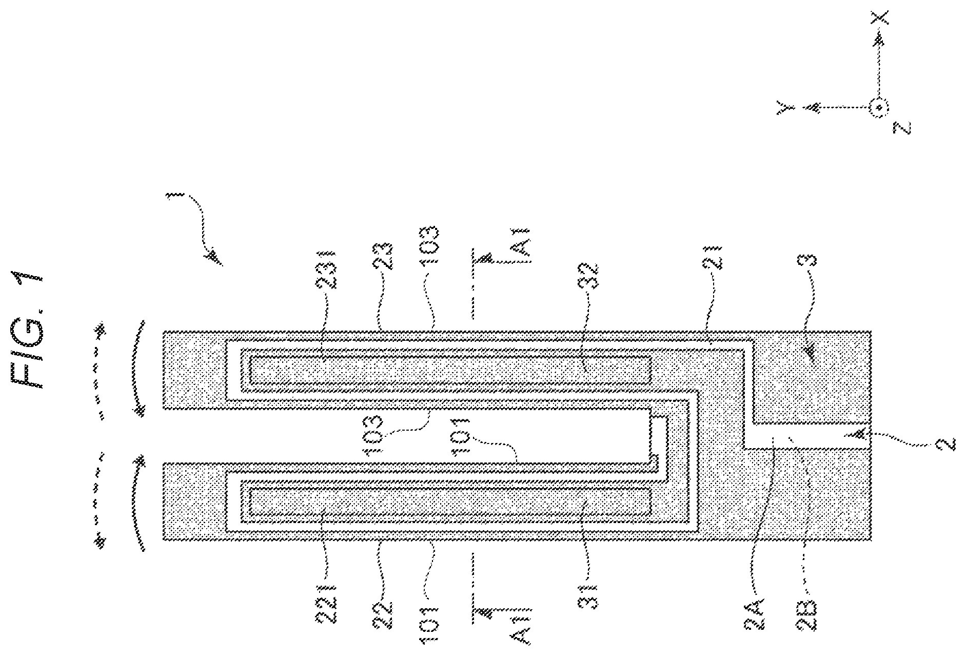
The vibration element 1 is a tuning-fork-type vibration element and includes a vibration substrate 2 and an electrode 3 formed at the front surface of the vibration substrate 2 , as shown in .
The vibration substrate 2 is formed by patterning a Z-cut quartz crystal substrate as a Z-cut quartz crystal plate into a desired shape, spreads in the plane X-Y defined by the axes X and Y, which are the crystal axes of quartz crystal, and has a thickness in the direction Z. The axis X is also called an electrical axis, the axis Y is also called a mechanical axis, and the axis Z is also called an optical axis.
The vibration substrate 2 has the shape of a plate and has a first surface 2 A and a second surface 2 B, which are front and rear sides with respect with each other and arranged side by side in the direction Z. The vibration substrate 2 has a base 21 , and a first vibrating arm 22 and a second vibrating arm 23 extending from the base 21 along the direction Y and arranged side by side along the direction X.
The first vibrating arm 22 has a bottomed first groove 221 , which opens to the first surface 2 A, a bottomed second groove 222 , which opens to the second surface 2 B, and a side surface 101 , which couples the first surface 2 A and the second surface 2 B to each other. Similarly, the second vibrating arm 23 has a bottomed first groove 231 , which opens to the first surface 2 A, a bottomed second groove 232 , which opens to the second surface 2 B, and a side surface 103 , which couples the first surface 2 A and the second surface 2 B to each other. The first grooves 221 and 231 and the second grooves 222 and 232 extend along the direction Y, and the inner surface of each of the grooves forms a bottom surface 111 , in-groove side surfaces 112 and 113 , and inclining surfaces 114 and 115 . The in-groove side surfaces 112 and 113 face each other, the in-groove side surface 112 , which faces the negative side of the direction X, is coupled to the bottom surface 111 via the inclining surface 114 , and the in-groove side surface 113 , which faces the positive side of the direction X, is coupled to the bottom surface 111 via the inclining surface 115 . The first vibrating arm 22 and the second vibrating arm 23 thus each have a substantially H-shaped cross-sectional shape. The thus configured vibration element 1 has a reduced thermoelastic loss and excellent vibration characteristics. The bottom surfaces 111 are each a portion at the deepest position in the direction Z separate from the first surface 2 A or the second surface 2 B, and may not necessarily be parallel to the plane X-Y. For example, the first grooves 221 and 231 and the second grooves 222 and 232 may be so shaped that the inclining surfaces 114 and 115 intersect with each other. In this case, the ridge line that couples the inclining surfaces 114 and 115 to each other corresponds to the bottom surface 111 .
The electrode 3 includes a signal electrode 31 and a ground electrode 32 . The signal electrode 31 is disposed at the first surface 2 A and the second surface 2 B of the first vibrating arm 22 and the side surface 103 of the second vibrating arm 23 . On the other hand, the ground electrode 32 is disposed at the side surface 101 of the first vibrating arm 22 and the first surface 2 A and the second surface 2 B of the second vibrating arm 23 . When a drive signal is applied to the signal electrode 31 with the ground electrode 32 grounded, the first vibrating arm 22 and the second vibrating arm 23 perform flexural vibration in the direction X, in which the two vibrating arms repeatedly approach each other and separate from each other, as indicated by the arrows in .
The vibration element 1 has been briefly described above.
The method for manufacturing the vibration element 1 will next be described. The method for manufacturing the vibration element 1 includes a preparation step S 1 of preparing a quartz crystal substrate 20 , which is the base material of the vibration substrate 2 , a first protective film formation step S 2 of forming a first protective film 5 at the first surface 2 A of the quartz crystal substrate 20 , a first dry etching step S 3 of dry-etching the quartz crystal substrate 20 from the side facing the first surface 2 A via the first protective film 5 , a second protective film formation step S 4 of forming a second protective film 6 at the second surface 2 B of the quartz crystal substrate 20 , a second dry etching step S 5 of dry-etching the quartz crystal substrate 20 from the side facing the second surface 2 B via the second protective film 6 , a wet etching step S 6 of wet-etching the quartz crystal substrate 20 , and an electrode formation step S 7 of forming the electrode 3 at the front surface of the vibration substrate 2 produced by the steps described above, as shown in .
The steps described above will be sequentially described below.
Preparation Step S 1
The quartz crystal substrate 20 , which is the base material of the vibration substrate 2 , is prepared, as shown in . The quartz crystal substrate 20 has been prepared, for example, by chemical mechanical polishing (CMP) in the form of a substrate having a desired thickness and has a sufficiently smooth first surface 2 A and second surface 2 B. A plurality of vibration elements 1 are formed all at once from the quartz crystal substrate 20 .
First Protective Film Formation Step S 2
A metal film M 1 is deposited at the first surface 2 A of the quartz crystal substrate 20 , and a metal film M 2 is deposited at the second surface 2 B of the quartz crystal substrate 20 , as shown in . Thereafter, a first photoresist film R 1 is deposited on the metal film M 1 , and the deposited first photoresist film R 1 is patterned. Thereafter, the first protective film 5 is deposited at the openings of the first resist film R 1 , and then the first photoresist film R 1 is removed. As a result, the structure shown in is achieved. The first protective film 5 is not particularly limited to a specific film and can be any of a variety of metal masks that are resistant to etching, such as a nickel mask.
The first protective film 5 has openings 51 , 52 , and 53 in portions where the quartz crystal substrate 20 should be removed. Out of the openings, the opening 51 coincides with a first groove formation area Q 1 , where the first grooves 221 and 231 are formed. The opening 52 coincides with an inter-arm area Q 4 , which is located between a first vibrating arm formation area Q 2 , where the first vibrating arm 22 is formed, and a second vibrating arm formation area Q 3 , where the second vibrating arm 23 is formed. The opening 53 coincides with an inter-device area Q 5 , which is located between adjacent vibration substrates 2 . That is, the first protective film 5 is formed in the area excluding the first groove formation area Q 1 , the inter-arm area Q 4 , and the inter-device area Q 5 .
First Dry Etching Step S 3
The quartz crystal substrate 20 is dry-etched from the side facing the first face 2 A via the first protective film 5 to simultaneously form the first grooves 221 and 231 in the first surface 2 A and the outer shape of the vibration substrate 2 , that is, the outer shapes of the first vibrating arm 22 and the second vibrating arm 23 , as shown in . The phrase “simultaneously form” means that two features are formed all at once in a single step. More specifically, the present step is reactive ion etching and is performed by using a reactive ion etching apparatus (RIE apparatus). The reaction gas introduced into the RIE apparatus is not limited to a specific gas and may, for example, be SF 6 , CF 4 , C 2 F 4 , C 2 F 6 , C 3 F 6 , or C 4 F 8 .
The present step ends when the first grooves 221 and 231 reach a desired depth. It is known that the “micro-loading effect”, which lowers the etching rate as the pattern density of the first protective film 5 increases, occurs in dry etching. In the present embodiment, comparison between a width W of each of the first grooves 221 and 231 , which is the width in the direction X, and a width A of the inter-arm area Q 4 , which is the width in the direction X, shows that W<A. Comparison between the width W and a width B of the inter-device area Q 5 , which is the width in the direction X, shows that W<B. The micro-loading effect therefore causes the etching rate in the first groove formation area Q 1 to be lower than that in the inter-arm area Q 4 and the inter-device area Q 5 . Therefore, at the end of the present step, a depth Wa of the first grooves 221 and 231 is smaller than depths Aa and Ba of the outer shape of the vibration substrate 2 . That is, Wa<Aa (Wa/Aa<1) and Wa<Ba (Wa/Ba<1) are satisfied. The depths Aa and Ba are each greater than or equal to half the thickness of the quartz crystal substrate 20 . That is, let Ta be the thickness of the quartz crystal substrate 20 , and Aa ≥0.5 Ta and Ba ≥0.5 Ta are satisfied.
After the present step is completed, the first protective film 5 and the metal film M 1 are removed, and the rear surface of the quartz crystal substrate 20 is ready to be processed.
Second Protective Film Formation Step S 4
The second protective film 6 is deposited on the metal film M 2 , as shown in . The method for depositing the second protective 6 film is the same as the aforementioned method for depositing the first protective film 5 . The second protective film 6 has openings 61 , 62 , and 63 in portions where the quartz crystal substrate 20 should be removed. Out of the openings, the opening 61 coincides with a second groove formation area Q 6 , where the second grooves 222 and 232 are formed. The opening 62 coincides with the inter-arm area Q 4 . The opening 63 coincides with the inter-device area Q 5 .
Second Dry Etching Step S 5
The quartz crystal substrate 20 is dry-etched from the side facing the second face 2 B via the second protective film 6 to simultaneously form the second grooves 222 and 232 in the second surface 2 B and the outer shape of the vibration substrate 2 , that is, the outer shapes of the first vibrating arm 22 and the second vibrating arm 23 , as illustrated in . The present step is executed as the first dry etching step S 3 is.
The present step ends when the second grooves 222 and 232 reach a desired depth. In the present embodiment, comparison between the width W of the second grooves 222 and 232 , which is the width in the direction X, and the width A of the inter-arm area Q 4 , which is the width in the direction X, shows that W<A. Comparison between the width W and the width B of the inter-device area Q 5 , which is the width in the direction X, shows that W<B. The micro-loading effect therefore causes the etching rate in the second groove formation area Q 6 to be lower than that in the inter-arm area Q 4 and the inter-device area Q 5 . Therefore, at the end of the present step, the depth Wa of the second grooves 222 and 232 is smaller than the depths Aa and Ba of the outer shape of the vibration substrate 2 . That is, Wa<Aa (Wa/Aa<1) and Wa<Ba (Wa/Ba<1) are satisfied. The depths Aa and Ba are each greater than or equal to half the thickness of the quartz crystal substrate 20 . That is, Aa ≥0.5 Ta and Ba ≥0.5 Ta are satisfied. The inter-arm area Q 4 and the inter-device area Q 5 therefore pass through the quartz crystal substrate 20 . The inter-arm area Q 4 and the inter-device area Q 5 passing through the quartz crystal substrate 20 form the first vibrating arm 22 and the second vibrating arm 23 .
After the present step is completed, the second protective film 6 and the metal film M 2 are removed, as shown in .
As described above, in the first dry etching step S 3 , the quartz crystal substrate 20 is dry-etched from the side facing the first surface 2 A, and in the second dry etching step S 5 , the quartz crystal substrate 20 is dry-etched from the side facing the second surface 2 B to form the outer shape of the vibration substrate 2 . Therefore, for example, when the positions of the first protective film 5 and the second protective film 6 shift from each other in the plan view viewed in the direction Z due to manufacturing variations, a stepped portion is formed in some cases in each of the side surface 101 of the first vibrating arm 22 and the side surface 103 of the second vibrating arm 23 in an area 105 , where the dry etching in the first dry etching step S 3 and the dry etching in the second dry etching step S 5 are both performed.
For example, when the position of the second protective film 6 shifts toward the negative side of the direction X from the position of the first protective film 5 , a stepped portion 107 is formed at the side surface 101 of the first vibrating arm 22 because the outer shape of the vibration substrate 2 formed in the second dry etching step S 5 shifts toward the negative side of the direction X from the outer shape of the vibration substrate 2 formed in the first dry etching step S 3 , as shown in . Similarly, when the position of the second protective film 6 shifts toward the positive side of the direction X from the position of the first protective film 5 , for example, the stepped portion 107 is formed. The above description has been made with reference to the first vibrating arm 22 by way of example, and the stepped portion 107 is similarly formed at the side surface 103 of the second vibrating arm 23 when position of the second protective film 6 shifts from the position of the first protective film 5 .
Wet Etching Step S 6
The wet etching step S 6 is the step of wet-etching the quartz crystal substrate 20 by immersing the quartz crystal substrate 20 in an etchant. The etchant can be hydrofluoric acid or ammonium fluoride.
The first vibrating arm 22 and the second vibrating arm 23 are formed as part of the quartz crystal substrate 20 by the first dry etching step S 3 and the second dry etching step S 5 , as described above. That is, the present step is the step of wet-etching the first vibrating arm 22 and the second vibrating arm 23 , and specifically, the step of wet-etching the side surfaces 101 and 103 , the first grooves 221 and 231 , and the second grooves 222 and 232 of the first vibrating arm 22 and the second vibrating arm 23 . In the present step, wet-etching the side surfaces 101 and 103 of the first vibrating arm 22 and the second vibrating arm 23 allows reduction in the size of the stepped portions 107 formed at the side surfaces 101 and 103 . Smaller stepped portions 107 prevent unwanted vibration from occurring when the vibration element 1 is caused to vibrate and the vibration element 1 from being damaged when impact acts thereon.
In the present step, wet-etching the first grooves 221 and 231 and the second grooves 222 and 232 causes the inner surfaces of the first grooves 221 and 231 and the second grooves 222 and 232 to form the inclining surfaces 114 and 115 and the bottom surfaces 111 , as shown in .
Let D 1 be the depth of a groove formed in the first dry etching step S 3 and the second dry etching step S 5 , and D 2 be the depth of a groove formed in the wet etching step S 6 , and the final groove depth D after the wet etching step S 6 , that is, the distance in the direction Z from the first surface 2 A or the second surface 2 B to the bottom surface 111 is D 1 +D 2 . The depth D 1 is equal to the depth Wa described above. The depth D 1 can be regarded as the distance in the direction Z from one of the boundary between the in-groove side surface 112 and the inclining surface 114 and the boundary between the in-groove side surface 113 and the inclining surface 115 , the boundary farther from the bottom surface 111 , to the first surface 2 A or second surface 2 B. The depth D 2 can be regarded as the distance in the direction Z from the aforementioned boundary farther from the bottom surface 111 to the bottom surface 111 . In the present embodiment, the depth D 1 is the distance in the direction Z from the boundary between the in-groove side surface 112 and the inclining surface 114 to the first surface 2 A or the second surface 2 B, and the depth D 2 is the distance in the direction Z from that boundary to the bottom surface 111 . That is, the depth D 2 is the length of the inclining surface 114 in the direction Z, and depth D 1 is the result of subtraction of the depth D 2 from the depth D.
is a graph showing the result of a simulation of the relationship between a dry ratio D 1 /D and a Q value ratio. The dry ratio D 1 /D is the ratio of the depth D 1 of the groove formed by the dry etching to the final depth D of the groove. The Q value ratio is a normalized Q value of the vibration element 1 , provided that the Q value of the vibration element 1 manufactured under the condition that the dry ratio D 1 /D is 0, that is, the Q value achieved when the first grooves 221 and 231 and the second grooves 222 and 232 are formed only by the wet etching is regarded as 100%. The Q value of the vibration element 1 changes in accordance with a change in the dry ratio D 1 /D, as shown in . Specifically, as the dry ratio D 1 /D increases, the Q value also increases, and when the dry ratio D 1 /D falls within a range D 1 /D ≥0.80, the Q value is substantially constant. The substantially constant Q value is comparable to the Q value achieved when the dry ratio D 1 /D is 1.00, that is, the Q value achieved when an ideally shaped first vibration arm 22 and second vibration arm 23 with no stepped portion 107 are formed by the dry etching alone. Forming the first grooves 221 and 231 and the second grooves 222 and 232 in such a way that the dry ratio D 1 /D ≥0.80 is satisfied as described above can greatly improve the Q value as compared with the case where the grooves are formed by the dry etching alone.
shows graphs illustrating the results of the simulation of the relationship between the dry ratio D 1 /D and the Q-value ratio in response to changes in an aspect ratio D/W, which is the ratio of the groove depth D to the groove width W. Even when the aspect ratio D/W changes, causing the dry ratio D 1 /D to fall withing the range D 1 /D ≥0.80 can greatly improve the Q value, as shown in . Furthermore, forming the first grooves 221 and 231 and the second grooves 222 and 232 in such a way that the dry ratio D 1 /D falls within a range D 1 /D ≥0.85 can achieve a better Q value.
In the wet etching step S 6 , the amount by which the side surfaces 101 and 103 are etched is preferably greater than or equal to 0.01 μm. The thus set etching amount reduces the size of the stepped portions 107 , preventing unwanted vibration from occurring when the vibration element 1 is caused to vibrate and the vibration element 1 from being damaged when impact acts thereon. The amount by which the side surfaces 101 and 103 are etched is the amount of displacement, before and after the wet etching step S 6 , of the side surfaces 101 and 103 in the direction X, which is the direction perpendicular to the side surfaces 101 and 103 .
In addition, in the present step, the amount by which the side surfaces 101 and 103 are etched is preferably smaller than or equal to 1 μm. When the amount by which the side surfaces 101 and 103 are etched exceeds 1 μm, each portion of the vibration substrate 2 excluding the stepped portions 107 , for example, the first surface 2 A, the second surface 2 B, the first grooves 221 and 231 , and the second grooves 222 and 232 are wet-etched, so that the outer shape of the vibration element 1 undesirably has dimensions different from desired values. The vibration element 1 can therefore undesirably vibrate at a frequency far off a desired frequency. Maintaining the amount by which the side surfaces 101 and 103 are etched smaller than or equal to 1 μm allows suppression of deviation from the desired frequency.
Furthermore, in the present step, the amount by which the side surfaces 101 and 103 are etched is preferably smaller than or equal to 0.5 μm. When the amount by which the side surfaces 101 and 103 are etched exceeds 0.5 μm, the corners of the vibrating arms 22 and 23 , where the first surface 2 A and the second surface 2 B are coupled to the side surfaces 101 and 103 , and other portions are wet-etched, resulting in a complicated shape of the vibration element 1 that differs from a desired shape. Unwanted vibration may therefore occur when the vibration element 1 is caused to vibrate, resulting in deterioration of the vibration characteristics, such as the Q value. Maintaining the amount by which the side surfaces 101 and 103 are etched smaller than or equal to 0.5 μm allows suppression of occurrence of undesired vibration.
A plurality of vibration substrates 2 are collectively formed from the quartz crystal substrate 20 by executing steps S 1 to S 6 described above.
Electrode Formation Step S 7
A metal film is deposited at the front surface of the vibration substrate 2 , and the metal film is patterned to form the electrode 3 .
The vibration element 1 is thus manufactured.
As described above, the dry etching allows processing without being affected by the crystal planes of the quartz crystal, thus achieving excellent dimensional accuracy. Forming the first grooves 221 and 231 , the second grooves 222 and 232 , and the outer shape of the vibration substrate 2 all at once allows reduction in the number of steps of manufacturing the vibration element 1 and the cost of the vibration element 1 . Furthermore, positional shift of the first grooves 221 and 231 and the second grooves 222 and 232 from the outer shape is prevented, whereby the accuracy of formation of the vibration substrate 2 increases.
The wet etching allows reduction in the size of the stepped portions 107 formed at the side surface 101 of the first vibrating arm 22 and the side surface 103 of the second vibrating arm 23 when the quartz crystal substrate 20 is dry-etched from both the sides facing the first surface 2 A and the second surface 2 B. The smaller stepped portions 107 can suppress unwanted vibration that occurs when the vibration element 1 is caused to vibrate and damage made to the vibration element 1 when impact acts thereon.
The method for manufacturing the vibration element 1 has been described above.
The conditions under which the micro-loading effect more reliably manifests itself will next be described with reference to .
shows the relationship between W/A and Wa/Aa for different etching periods. As can be seen from , the micro-loading effect notably manifests itself at each point of time in the region where W/A ≤40% is satisfied.
The micro-loading effect manifests itself in a variety of manners in accordance with the type of reaction gas used in the dry etching. shows the relationship between W/A and Wa/Aa in a case where three typical reaction gases different from one another are used.
For example, when a fluorine-based gas having a large carbon content, such as C 2 F 4 , C 2 F 6 , C 3 F 6 , and C 4 F 8 , is used as the reaction gas, a thick sidewall protective film is produced, and the slope of the graph representing the relationship decreases, as in the case of a gas type G 3 . Wa/Aa therefore tends to increase with the width A being smaller than the width W, whereby the size of the vibration element 1 can be reduced. For example, to design the frequency and the CI value of the vibration element 1 , a width W greater than or equal to a certain value and a depth Wa close to the depth Aa are required in some cases. In the design process, the width A needs to be a small value to reduce the size of the vibration element 1 , and at least one of C 2 F 4 , C 2 F 6 , C 3 F 6 , and C 4 F 8 is particularly effective in this case.
On the other hand, when a fluorine-based gas containing little or no carbon, such as SF 6 and CF 4 , is used alone or in combination with a fluorine-based gas having a large carbon content, a thin sidewall protective film is produced, and the slope of the graph increases, as in the case of a gas type G 1 . The width A can therefore be greater than the width W with the depth Wa maintained greater than the depth Aa. For example, when it is desired to achieve a narrow first vibrating arm 22 and second vibrating arm 23 but a large width A while achieving a large depth Wa, at least one of SF 6 and CF 4 is particularly effective.
Let x be W/A and y be Wa/Aa, and the gas type G 1 is expressed by Expression (1) below, a gas type G 2 is expressed by Expression (2) below, and the gas type G 3 is expressed by Expression (3) below. y=− 4.53×10 −6 x 4 +3.99×10 −4 x 3 −1.29×10 −3 x 2 +1.83×10 −1 x (1) y=− 5.59×10 −8 x 4 +1.48×10 −5 x 3 −1.43×10 −3 x 2 +6.09×10 −2 x (2) y=− 6.90×10 −10 x 4 +5.47×10 −7 x 3 −1.59×10 −4 x 2 +2.03×10 −2 x (3)
When y is in a region P between the graphs expressed by Expressions (1) and (3), as shown in , that is, when y satisfies Expressions (4) and (5) below, the micro-loading effect more reliably manifests itself with a typical reaction gas. Therefore, the vibration element 1 can be readily manufactured, and the manufacturing cost thereof can be reduced. y≥− 4.53×10 −6 x 4 +3.99×10 −4 x 2 −1.29×10 −3 x 2 +1.83×10 −1 x (4) y≤− 6.90×10 −10 x 4 +5.47×10 −7 x 3 −1.59×10 −4 x 2 +2.03×10 −2 x (5)
When y does not satisfy Expression (4), the change in the depth Wa is greater than the change in the width W, so that the depth Wa may undesirably vary. The variation can be suppressed by y that satisfies Expression (4). When y does not satisfy Expression (5), it is difficult to increase y in regions where x is large, and the depth Wa decreases. To increase the depth Wa, a condition closer to W=A needs to be achieved, which tends to cause geometrical constraints. The geometrical constraints can be suppressed by y that satisfies Expression (5).
For example, when the width W and the depth Wa are fixed, selecting the gas type G 2 allows reduction in the width A as compared with the width A achieved when the gas type G 1 is selected and therefore allows reduction in the size of the vibration element 1 . Selecting the gas type G 3 allows further reduction in the width A as compared with the width A achieved when the gas type G 2 is selected and therefore allows further reduction in the size of the vibration element 1 . As described above, from the viewpoint of size reduction, it is preferable that y is in the region P, and it is more preferable that y is in a region PP between the graphs expressed by Expressions (2) and (3). That is, it is preferable that y satisfies Expression (6) below and Expression (5) described above. y≥− 5.59×10 −8 x 4 +1.48×10 −5 x 3 −1.43×10 −3 x 2 +6.09×10 −2 x (6)
The effect of improvement of the CI value of the vibration element 1 provided when the first grooves 221 and 231 and the second grooves 222 and 232 are formed will next be described with reference to .
shows the relationship between Wa/Aa and a CI ratio. The CI ratio is a normalized CI value of the vibration element 1 , provided that the CI value of the vibration element 1 manufactured under the condition that none of the first grooves 221 and 231 and the second grooves 222 and 232 is formed is regarded as 1.0. It is preferable that Wa/Aa ≥0.2 is satisfied, as shown in . Note that Wa/Aa <1 is satisfied in the present embodiment, in which the micro-loading effect is used. The condition described above allows reduction in the CI value to at least 30% of the CI value achieved when none of the first grooves 221 and 231 and the second grooves 222 and 232 is formed. A vibration element 1 excellent vibration having characteristics can therefore be manufactured. It is further preferable that Wa/Aa ≥0.4 is satisfied, in which case, the CI value can be reduced to at least 10% of the CI value achieved when none of the first grooves 221 and 231 and the second grooves 222 and 232 is formed.
The conditions under which the micro-loading effect more reliably manifests itself in the method for manufacturing the vibration element 1 have been described above.
As described above, the method for manufacturing the vibration element 1 is a method for manufacturing a vibration element that includes the first vibrating arm 22 and the second vibrating arm 23 , which extend along the direction Y, which is the first direction, and are arranged side by side along the direction X, which is the second direction and intersects with the direction Y, the first vibrating arm 22 and the second vibrating arm 23 each having the first surface 2 A and the second surface 2 B, which are front and rear sides with respect with each other and are arranged side by side in the direction Z, which is the third direction and intersects with the directions X and Y, the first vibrating arm 22 and the second vibrating arm 23 further having the bottomed first grooves 221 and 231 , which open to the first surface 2 A, the bottomed second grooves 222 and 232 , which open to the second surface 2 B, and the side surfaces 101 and 103 , which couple the first surface 2 A and the second surface 2 B to each other, the method including the preparation step S 1 of preparing the quartz crystal substrate 20 having the first surface 2 A and the second surface 2 B, the first dry etching step S 3 of dry-etching the quartz crystal substrate 20 from the side facing the first surface 2 A to form the first grooves 221 and 231 and the outer shapes of the first vibrating arm 22 and the second vibrating arm 23 , the second dry etching step S 5 of dry-etching the quartz crystal substrate 20 from the side facing the second surface 2 B to form the second grooves 222 and 232 and the outer shapes of the first vibrating arm 22 and the second vibrating arm 23 , and the subsequent wet etching step S 6 of wet-etching the side surfaces 101 and 103 of the first vibrating arm 22 and the second vibrating arm 23 , the first grooves 221 and 231 , and the second grooves 222 and 232 to form the inclining surfaces 114 and 115 , which couple the bottom surfaces 111 of the first grooves 221 and 231 and the second grooves 222 and 232 to the in-groove side surfaces 112 and 113 , and the first grooves 221 and 231 and the second grooves 222 and 232 satisfy D 1 /D ≥ 0 . 80 , where D represents the depth of the first grooves 221 and 231 and the second grooves 222 and 232 , and D 1 represents the result of subtraction of the length of the inclining surface 114 in the direction Z from the depth.
According to the manufacturing method described above, the size of the stepped portions 107 formed at the side surfaces 101 and 103 of the first vibrating arm 22 and the second vibrating arm 23 can be reduced. The stepped portions 107 having the reduced size can suppress unwanted vibration that occurs when the vibration element 1 is caused to vibrate and damage made to the vibration element 1 when impact acts thereon. Furthermore, the dry ratio D 1 /D satisfies D 1 /D ≥0.80, whereby the Q value can be improved, as described above.
In the method for manufacturing the vibration element 1 , it is preferable that the first grooves 221 and 231 and the second grooves 222 and 232 are formed under the condition that the dry ratio D 1 /D satisfies D 1 /D ≥0.85, as described above. The Q value can thus be improved.
In the method for manufacturing the vibration element 1 , it is preferable that the amount by which the side surfaces 101 and 103 are etched in the wet etching step S 6 is greater than or equal to 0.01 μm, as described above. The thus set etching amount reduces the size of the stepped portions 107 , preventing unwanted vibration from occurring when the vibration element 1 is caused to vibrate and the vibration element 1 from being damaged when impact acts thereon.
In the method for manufacturing the vibration element 1 , it is preferable that the amount by which the side surfaces 101 and 103 are etched in the wet etching step S 6 is smaller than or equal to 1 μm, as described above. Deviation from the desired frequency that occurs when the vibration element 1 is caused to vibrate can thus be suppressed.
In the method for manufacturing the vibration element 1 , it is preferable that the amount by which the side surfaces 101 and 103 are etched in the wet etching step S 6 is smaller than or equal to 0.5 μm, as described above. Unwanted vibration that occurs when the vibration element 1 is caused to vibrate can thus be suppressed.
In the method for manufacturing the vibration element 1 , it is preferable that Wa/Aa <1 is satisfied in at least one of the first dry etching step S 3 and the second dry etching step S 5 , as described above, where Wa represents the depth of the first grooves 221 and 231 formed in the first dry etching step S 3 and the depth of the second grooves 222 and 232 formed in the second dry etching step S 5 , and Aa represents the depth of the outer shapes of the first vibrating arm 22 and the second vibrating arm 23 formed in the first dry etching step S 3 and the depth of the outer shapes of the first vibrating arm 22 and the second vibrating arm 23 formed in the second dry etching step S 5 . The first grooves 221 and 231 , the second grooves 222 and 232 , and the outer shape of the vibration substrate 2 can thus be formed all at once. The number of steps of manufacturing the vibration element 1 and the cost of the vibration element 1 can therefore be reduced. Furthermore, positional shift of the first grooves 221 and 231 and the second grooves 222 and 232 from the outer shape is prevented, whereby the accuracy of formation of the vibration substrate 2 increases.
2. Second Embodiment
The method for manufacturing the vibration element 1 according to a second embodiment will be described with reference to to 21 . The same components as those in the first embodiment have the same reference characters, and no redundant description of the same components will be made.
The second embodiment is the same as the first embodiment except that a third protective film formation step S 10 is provided between the second dry etching step S 5 and the wet etching step S 6 , that third protective films 109 are formed at the first surface 2 A and the second surface 2 B of the quartz crystal substrate 20 in the third protective film formation step S 10 , and that the first surface 2 A and the second surface 2 B of the quartz crystal substrate 20 is masked by the third protective film 109 in the wet etching process S 6 .
The method for manufacturing the vibration element 1 according to the second embodiment includes preparation step S 1 of preparing the quartz crystal substrate 20 , which is the base material of the vibration substrate 2 , the first protective film formation step S 2 of forming the first protective film 5 at the first surface 2 A of the quartz crystal 20 , the first dry etching step S 3 of dry-etching the quartz crystal substrate 20 from the side facing the first surface 2 A via the first protective film 5 , the second protective film formation step S 4 of forming the second protective film 6 at the second surface 2 B of the quartz crystal substrate 20 , the second dry etching step S 5 of dry-etching the quartz crystal substrate 20 from the side facing the second surface 2 B via the second protective film 6 , the third protective film formation step S 10 of forming the third protective films 109 at the first surface 2 A and the second surface 2 B of the quartz crystal substrate 20 , the wet etching step S 6 of wet-etching the quartz crystal substrate 20 , and the electrode formation step S 7 of forming the electrode 3 at the front surface of the vibration substrate 2 produced by the steps described above, as shown in .
The preparation step S 1 to the second dry etching step S 5 are the same as those in the first embodiment and will therefore not be described, and the third protective film formation step S 10 and the following steps will be described. The second protective film 6 and the metal film M 2 are removed from the quartz crystal substrate 20 after the completion of the second dry etching step S 5 , as in the first embodiment.
Third Protective Film Formation Step S 10
The third protective films 109 are formed at the first surface 2 A and the second surface 2 B of the quartz crystal substrate 20 , as shown in . The third protective films 109 are each, for example, a metal film formed by sequentially depositing chromium and gold from the side facing the quartz crystal substrate 20 . The third protective films 109 can be formed by depositing the metal films at the surfaces of the quartz crystal substrate 20 , for example, by using sputtering or chemical vapor deposition (CVD) and patterning the metal films by using photolithography and etching techniques.
Wet Etching Step S 6
In the present step, the quartz crystal substrate 20 is wet-etched by immersing the quartz crystal substrate 20 in an etchant.
In the second embodiment, prior to the present step, the third protective films 109 are formed at the first surface 2 A and the second surface 2 B of the quartz crystal substrate 20 in the third protective film formation step S 10 . Therefore, in the present step, the first surface 2 A and the second surface 2 B of the quartz crystal substrate 20 are masked by the third protective films 109 . In other words, the first surface 2 A and the second surface 2 B of the first vibrating arm 22 and the second vibrating arm 23 are masked by the third protective films 109 . That is, the first surface 2 A and the second surface 2 B of the first vibrating arm 22 and the second vibrating arm 23 are not wet-etched in the present step. The masking third protective films 109 prevents the dimensions and shape of the vibration element 1 from being different from the desired dimensions and shape. Deviation from the desired frequency and occurrence of unwanted vibration of the vibration element 1 can thus be suppressed.
Since no third protective film 109 is formed at the side surface 101 of the first vibrating arm 22 and the side surface 103 of the second vibrating arm 23 , the size of the stepped portions 107 formed at the side surfaces 101 and 103 can be reduced, as in the first embodiment.
After the present step is completed, the third protective films 109 are removed, as shown in . A plurality of vibration substrates 2 are thus collectively formed from the quartz crystal substrate 20 .
Electrode Formation Step S 7
The present step is executed in the same manner as in the first embodiment. A metal film is deposited at the front surface of the vibration substrate 2 , and the metal film is patterned to form the electrode 3 .
The vibration element 1 is thus manufactured.
The present embodiment can provide the following effect in addition to the effects provided by the first embodiment.
In the wet etching step S 6 , the first surface 2 A and the second surface 2 B of the quartz crystal substrate 20 are masked by the third protective films 109 , which prevent the dimensions and shape of the vibration device 1 from being different from the desired dimensions and shape. Deviation from the desired frequency and occurrence of unwanted vibration of the vibration element 1 can thus be suppressed.
The vibration element manufacturing method according to the present disclosure has been described above based on the first and second embodiments.
The present disclosure is, however, not limited thereto, and the configuration of each portion can be replaced with any configuration having the same function. Furthermore, any other constituent element may be added to any of the embodiments of the present disclosure. Moreover, the embodiments may be combined as appropriate with each other.
For example, in the embodiments described above, Wa/Aa <1 is satisfied in each of the first dry etching step S 3 and the second dry etching step S 5 , but not necessarily, and Wa/Aa <1 only needs to be satisfied in at least one of the steps.
The vibration element manufactured by the vibration element manufacturing method according to the present disclosure is not limited to a specific device and may, for example, be a vibration element 1 A shown in . In the vibration device 1 A, a pair of first grooves 221 are formed side by side in the direction X at the first surface 2 A of the first vibrating arm 22 , and a pair of second grooves 222 are formed side by side in the direction X at the second surface 2 B of the first vibrating arm 22 . Similarly, a pair of first grooves 231 are formed side by side in the direction X at the first surface 2 A of the second vibrating arm 23 , and a pair of second grooves 232 are formed side by side in the direction X at the second surface 2 B of the second vibrating arm 23 . In the configuration described above, the width W of each of the grooves tends to decrease because a plurality of grooves are arranged in one direction. It is therefore preferable to use at least one of SF 6 and CF 4 as the reaction gas in the first dry etching step S 3 and the second dry etching step S 5 . The depth of each of the grooves can therefore be a deep groove, whereby the CI value can be lowered.
The vibration device may instead be a double-tuning-fork-type vibration device 7 shown in . Note that no electrode is shown in . The double-tuning-fork-type vibration element 7 includes a pair of bases 711 and 712 , and a first vibrating arm 72 and a second vibrating arm 73 , which link the bases 711 and 712 to each other. The first vibrating arm 72 and the second vibrating arm 73 have bottomed first grooves 721 and 731 , which open to a first surface 7 A, and bottomed second grooves 722 and 732 , which open to a second surface 7 B.
The vibration element may still instead, for example, be a gyro vibration element 8 shown in to 28 . No electrode is shown in to 28 . The gyro vibration element 8 includes a base 81 , a pair of detection vibration arms 82 and 83 , which extend from the base 81 toward opposite sides of the direction Y, a pair of linkage arms 84 and 85 , which extend from the base 81 toward opposite sides of the direction X, drive vibration arms 86 and 87 , which extend from the tip of the linkage arm 84 toward opposite sides of the direction Y, and drive vibration arms 88 and 89 , which extend from the tip of the linkage arm 85 toward opposite sides of the direction Y. When an angular velocity ωz around the axis Z acts on the thus configured gyro vibration element 8 with the drive vibration arms 86 , 87 , 88 , and 89 undergoing flexural vibration in the direction labeled with an arrows SD in , the Coriolis force newly excites flexural vibration of the detection vibration arms 82 and 83 in the direction labeled with an arrows SS, and the angular velocity ωz is detected based on the electric charges outputted from the detection vibration arms 82 and 83 due to the flexural vibration.
The detection vibration arms 82 and 83 have bottomed first grooves 821 and 831 , which open to a first surface 8 A, and bottomed second grooves 822 and 832 , which open to a second surface 8 B. The driving vibrating arms 86 , 87 , 88 , and 89 have bottomed first grooves 861 , 871 , 881 , and 891 , which open to the first surface 8 A, and bottomed second grooves 862 , 872 , 882 , and 892 , which open to the second surface 8 B. In the thus configured gyro vibration element 8 , for example, pairs of vibrating arms adjacent to each other in the direction X, such as the detection vibration arm 82 and the drive vibration arm 86 , the detection vibration arm 82 and the drive vibration arm 88 , the detection vibration arm 83 and the drive vibration arm 87 , and the detection vibration arm 83 and the drive vibration arm 89 , can be regarded as the first and second vibrating arms.
In the case of the gyro vibration element 8 , the inter-arm areas Q 4 each need to have a large size for a structural reason. In such a case, the depth Wa may decrease in the region between the graphs expressed by Expressions (2) and (3) described above, undesirably resulting a decrease in sensitivity. It is therefore preferable to use the region between the graphs expressed by Expressions (1) and (2) described above.
The vibration element may still instead, for example, be a gyro vibration element 9 shown in to 31 . The gyro vibration element 9 has a base 91 , a pair of drive vibration arms 92 and 93 , which extend from the base 91 toward the positive side of the direction Y and arranged side by side in the direction X, and a pair of detection vibration arms 94 and 95 , which extend from the base 91 toward the negative side of the direction Y and arranged side by side in the direction X. When an angular velocity ωy around the axis Y acts on the thus configured gyro vibration element 9 with the drive vibration arms 92 and 93 undergoing flexural vibration in the direction labeled with the arrows SD in , the Coriolis force newly excites flexural vibration of the detection vibration arms 94 and 95 in the direction labeled with the arrows SS, and the angular velocity ωy is detected based on the electric charges outputted from the detection vibration arms 94 and 95 due to the flexural vibration.
The drive vibration arms 92 and 93 have bottomed first grooves 921 and 931 , which open to a first surface 9 A, and bottomed second grooves 922 and 932 , which open to a second surface 9 B. The detection vibration arms 94 and 95 have bottomed first grooves 941 and 951 , which open to the first surface 9 A, and bottomed second grooves 942 and 952 , which open to the second surface 9 B. In the thus configured gyro vibration element 9 , the drive vibration arms 92 and 93 or the detection vibration arms 94 and 95 form the first and second vibrating arms.
Figures (20)
Citations
This patent cites (10)
- US2007/0222342
- US2009/0077781
- US2023/0126632
- US2023/0127801
- US2023/0139089
- US2023/0155564
- US2007-013382
- US2007-259036
- US2009-081521
- US2018-148380