Touch Control Structure and Display Apparatus with Touch Signal Lines with Double-layer Region in a Corner Area
Abstract
A touch control structure includes a plurality of touch signal lines in a peripheral area. A respective touch signal line includes a double-layer structure in a double-layer region and a single-layer structure in a single-layer region. The peripheral area includes a first sub-area on a first side, a second sub-area on a second side, a third sub-area on a third side, a fourth sub-area on a fourth side, of the touch control area. The first sub-area includes a side region, and one or more corner regions. The double-layer region and the single-layer region are in the first sub-area, the first sub-area has a first shortest width along a direction from the touch control area to the first sub-area, the first shortest width is greater than a shortest width of at least one of sub-areas of the peripheral area other than the first sub-area.
Claims (19)
1 . A touch control structure, comprising a plurality of touch electrodes in a touch control area and a plurality of touch signal lines in a peripheral area; wherein a respective one of the plurality of touch signal lines comprises a double-layer structure in a double-layer region and a single-layer structure in a single-layer region; the peripheral area comprises a first sub-area on a first side of the touch control area, a second sub-area on a second side of the touch control area, a third sub-area on a third side of the touch control area, a fourth sub-area on a fourth side of the touch control area; the first sub-area comprises a side region, and one or more corner regions respectively at one or more corners of the touch control structure; wherein the double-layer region and the single-layer region are in the first sub-area, the first sub-area has a first shortest width along a direction from the touch control area to the first sub-area, the first shortest width is greater than a shortest width of at least one of sub-areas of the peripheral area other than the first sub-area; a plurality of adjacent double-layer structures in the double-layer region are respectively connected to a plurality of adjacent single-layer structures in the single-layer region; the double-layer region is at least partially in the one or more corner regions; and a region where the double-layer structure transitions to the single-layer structure is at least partially in the one or more corner regions.
18 . A touch control structure, comprising a plurality of touch electrodes in a touch control area and a plurality of touch signal lines in a peripheral area; wherein a respective one of the plurality of touch signal lines comprises a double-layer structure in a double-layer region and a single-layer structure in a single-layer region; the peripheral area comprises a first sub-area on a first side of the touch control area, a second sub-area on a second side of the touch control area, a third sub-area on a third side of the touch control area, a fourth sub-area on a fourth side of the touch control area; the first sub-area comprises a side region, and one or more corner regions respectively at one or more corners of the touch control structure; wherein the double-layer region and the single-layer region are in the first sub- area, the first sub-area has a first shortest width along a direction from the touch control area to the first sub-area, the first shortest width is greater than a shortest width of at least one of sub-areas of the peripheral area other than the first sub-area; a plurality of adjacent double-layer structures in the double-layer region are respectively connected to a plurality of adjacent single-layer structures in the single-layer region; the double-layer region is at least partially in the one or more corner regions; and at least two adjacent single-layer structures respectively in the first layer and the second layer are electrically connected to adjacent rows of touch electrodes.
19 . A touch control structure, comprising a plurality of touch electrodes in a touch control area and a plurality of touch signal lines in a peripheral area; wherein a respective one of the plurality of touch signal lines comprises a double-layer structure in a double-layer region and a single-layer structure in a single-layer region; the peripheral area comprises a first sub-area on a first side of the touch control area, a second sub-area on a second side of the touch control area, a third sub-area on a third side of the touch control area, a fourth sub-area on a fourth side of the touch control area; the first sub-area comprises a side region, and one or more corner regions respectively at one or more corners of the touch control structure; wherein the double-layer region and the single-layer region are in the first sub-area, the first sub-area has a first shortest width along a direction from the touch control area to the first sub-area, the first shortest width is greater than a shortest width of at least one of sub-areas of the peripheral area other than the first sub-area; a plurality of adjacent double-layer structures in the double-layer region are respectively connected to a plurality of adjacent single-layer structures in the single-layer region; and the double-layer region is at least partially in the one or more corner regions; wherein multiple first single-layer structures respectively of multiple touch signal lines of the plurality of touch signal lines are clustered in a second region; multiple second single-layer structures respectively of the multiple touch signal lines of the plurality of touch signal lines are clustered in a third region; the multiple second single-layer structures are respectively connected to the multiple first single-layer structures; the multiple first single-layer structures are substantially parallel to each other, and respectively extend along a second direction; the multiple second single-layer structures are substantially parallel to each other, and respectively extend along a third direction; at least two of the multiple second single-layer structures are respectively in the first layer and the second layer; and the second direction and the third direction are different from each other, and intersecting each other at an angle greater than zero.
Show 16 dependent claims
2 . The touch control structure of claim 1 , wherein at least two of the plurality of adjacent single-layer structures are respectively in a first layer and a second layer; and the touch control structure further comprises a touch insulating layer between the first layer and the second layer.
3 . The touch control structure of claim 1 , wherein a first sub-region is a sub-region where multiple touch signal lines are connected to an integrated circuit.
4 . The touch control structure of claim 1 , wherein the double-layer region is at least partially in at least one of the second sub-area, the third sub-area, or the fourth sub-area.
5 . The touch control structure of claim 1 , wherein the single-layer region is in the side region.
6 . The touch control structure of claim 1 , wherein a respective double-layer structure comprises a first portion in the first layer and a second portion in the second layer; a first adjacent respective single-layer structure in the second layer is connected to a respective second portion of a first adjacent double-layer structure; and a second adjacent respective single-layer structure in the first layer is connected to a respective first portion of a second adjacent double-layer structure.
7 . The touch control structure of claim 6 , wherein the first portion and the second portion are connected through a connecting via extending through the touch insulating layer.
8 . The touch control structure of claim 1 , wherein multiple first double-layer structures respectively of multiple touch signal lines of the plurality of touch signal lines are clustered in a first region; multiple first single-layer structures respectively of the multiple touch signal lines of the plurality of touch signal lines are clustered in a second region; the multiple first double-layer structures are substantially parallel to each other, and respectively extend along a first direction; the multiple first single-layer structures are substantially parallel to each other, and respectively extend along a second direction; at least two of the multiple first single-layer structures are respectively in the first layer and the second layer; and the first direction and the second direction are different from each other, and intersecting each other at an angle greater than zero.
9 . The touch control structure of claim 8 , wherein multiple connecting points respectively connecting the multiple first double-layer structures and the multiple first single-layer structures are arranged along a seventh direction; and the second direction and the seventh direction intersect each other at an angle in a range of 6 degrees to 15 degrees.
10 . The touch control structure of claim 1 , wherein the plurality of touch electrodes comprise a plurality of first mesh electrodes arranged in a plurality of rows and a plurality of second mesh electrodes arranged in a plurality of columns; and the plurality of first mesh electrodes and the plurality of second mesh electrodes are in the second layer.
11 . The touch control structure of claim 10 , further comprising: a plurality of touch electrode bridges in the first layer; and vias extending through the touch insulating layer; wherein the plurality of touch electrode bridges respectively extend through the vias to respectively connect adjacent second mesh blocks in a respective column of a plurality of column of the plurality of second mesh electrodes.
12 . The touch control structure of claim 10 , wherein the plurality of touch signal lines comprise: a plurality of first touch signal lines respectively connected to the plurality of first mesh electrodes; a plurality of second touch signal lines respectively connected to first terminals of the plurality of second mesh electrodes; and a plurality of third touch signal lines respectively connected to second terminals of the plurality of second mesh electrodes.
13 . The touch control structure of claim 1 , wherein multiple second single-layer structures respectively of multiple touch signal lines of the plurality of touch signal lines are clustered in a third region; multiple second double-layer structures respectively of the multiple touch signal lines of the plurality of touch signal lines are clustered in a fourth region; the multiple second single-layer structures are substantially parallel to each other, and respectively extend along a third direction; the multiple second double-layer structures are substantially parallel to each other, and respectively extend along a fifth direction; at least two of the multiple second single-layer structures are respectively in the first layer and the second layer; the multiple second single-layer structures are respectively connected to the multiple second double-layer structures; and multiple second connecting points respectively connecting the multiple second single-layer structures and the multiple second double-layer structures are arranged along a sixth direction.
14 . The touch control structure of claim 1 , wherein multiple third double-layer structures respectively of multiple touch signal lines of the plurality of touch signal lines are clustered in a fifth region; multiple fourth double-layer structures respectively of the multiple touch signal lines of the plurality of touch signal lines are clustered in a sixth region; multiple third single-layer structures respectively of the multiple touch signal lines of the plurality of touch signal lines are clustered in a seventh region; a respective one of the multiple third single-layer structures is a half loop structure connecting a respective one of the multiple third double-layer structures and a respective one of the multiple fourth double-layer structures; the half loop structure comprises two parallel portions respectively extending along a second direction and a connecting portion connecting the two parallel portions together; at least two of the multiple third single-layer structures are respectively in the first layer and the second layer; the multiple third double-layer structures are substantially parallel to each other, and respectively extend along a first direction; the multiple fourth double-layer structures are substantially parallel to each other, and respectively extend along the first direction; and the first direction and the second direction are different from each other, and intersecting each other at an angle greater than zero.
15 . The touch control structure of claim 14 , wherein multiple fourth single-layer structures respectively of the multiple touch signal lines of the plurality of touch signal lines are clustered in an eighth region; the multiple fourth single-layer structures are respectively connected to the multiple third double-layer structures; the multiple fourth single-layer structures are substantially parallel to each other, and respectively extend along the second direction; and the multiple fourth single-layer structures are at least a sub-set of multiple first single-layer structures.
16 . The touch control structure of claim 1 , wherein the respective one of the plurality of touch signal lines has a line width in a range of 2.5 μm to 4.5 μm; orthographic projections of adjacent single-layer structures on a base substrate are spaced apart by a shortest distance in a range of 1.1 μm to 3.1 μm; orthographic projections of adjacent single-layer structures in the first layer on the base substrate are spaced apart by a shortest distance in a range of 4.7μm to 10.7 μm; and orthographic projections of adjacent single-layer structures in the second layer on the base substrate are spaced apart by a shortest distance in a range of 4.7 μm to 10.7 μm.
17 . A display apparatus, comprising: a display panel; the touch control structure of claim 1 ; and an integrated circuit.
Full Description
Show full text →
CROSS-REFERENCE TO RELATED APPLICATION
This application is a continuation of U.S. application Ser. No. 18/473,616, filed Sep. 25, 2023, which is a continuation of U.S. application Ser. No. 17/438,777, filed Dec. 4, 2020, which is a national stage application under 35 U.S.C. § 371 of International Application No. PCT/CN2020/133924, filed Dec. 4, 2020. Each of the forgoing applications is herein incorporated by reference in its entirety for all purposes.
TECHNICAL FIELD
The present invention relates to the field of display technology, more particularly, to a touch control structure and a display apparatus.
BACKGROUND
Various types of touch panels have been developed. Examples of touch panels include one-glass-solution (OGS) touch panels, on-cell touch panels, and in-cell touch panels. The on-cell touch panels provide high touch control accuracy. The on-cell touch panels can be classified into single-layer-on-cell (SLOC) touch panels and multi-layer-on-cell (MLOC) touch panels. In particular, multiple point touch control can be achieved in the MLOC touch panels with superior touch control accuracy and blanking effects.
SUMMARY
In one aspect, the present disclosure provides a touch control structure, comprising a plurality of touch electrodes in a touch control area and a plurality of touch signal lines in a peripheral area; wherein a respective one of the plurality of touch signal lines comprises a double-layer structure in a double-layer region and a single-layer structure in a single-layer region; the peripheral area comprises a first sub-area on a first side of the touch control area, a second sub-area on a second side of the touch control area, a third sub-area on a third side of the touch control area, a fourth sub-area on a fourth side of the touch control area; the first sub-area comprises a side region, and one or more corner regions respectively at one or more corners of the touch control structure; wherein the double-layer region and the single-layer region are in the first sub-area, the first sub-area has a first shortest width along a direction from the touch control area to the first sub-area, the first shortest width is greater than a shortest width of at least one of sub-areas of the peripheral area other than the first sub-area; a plurality of adjacent double-layer structures in the double-layer region are respectively connected to a plurality of adjacent single-layer structures in the single-layer region; and the double-layer region is at least partially in the one or more corner regions.
Optionally, at least two of the plurality of adjacent single-layer structures are respectively in a first layer and a second layer; and the touch control structure further comprises a touch insulating layer between the first layer and the second layer.
Optionally, the first sub-region is a sub-region where multiple touch signal lines are connected to an integrated circuit
Optionally, a region where the double-layer structure transitions to the single-layer structure is at least partially in the one or more corner regions.
Optionally, the double-layer region is at least partially in at least one of the second sub-area, the third sub-area, or the fourth sub-area.
Optionally, the single-layer region is in the side region.
Optionally, a respective double-layer structure comprises a first portion in the first layer and a second portion in the second layer; a first adjacent respective single-layer structure in the first layer is connected to a respective first portion of a first adjacent double-layer structure; and a second adjacent respective single-layer structure in the second layer is connected to a respective second portion of a second adjacent double-layer structure.
Optionally, the first portion and the second portion are connected through a connecting via extending through the touch insulating layer.
Optionally, multiple first double-layer structures respectively of multiple touch signal lines of the plurality of touch signal lines are clustered in a first region; multiple first single-layer structures respectively of the multiple touch signal lines of the plurality of touch signal lines are clustered in a second region; the multiple first double-layer structures are substantially parallel to each other, and respectively extend along a first direction; the multiple first single-layer structures are substantially parallel to each other, and respectively extend along a second direction; at least two of the multiple first single-layer structures are respectively in the first layer and the second layer; and the first direction and the second direction are different from each other, and intersecting each other at an angle greater than zero.
Optionally, multiple connecting points respectively connecting the multiple first double-layer structures and the multiple first single-layer structures are arranged along a seventh direction; and the second direction and the seventh direction intersect each other at an angle in a range of 6 degrees to 15 degrees.
Optionally, multiple first single-layer structures respectively of multiple touch signal lines of the plurality of touch signal lines are clustered in a second region; multiple second single-layer structures respectively of the multiple touch signal lines of the plurality of touch signal lines are clustered in a third region; the multiple second single-layer structures are respectively connected to the multiple first single-layer structures; the multiple first single-layer structures are substantially parallel to each other, and respectively extend along a second direction; the multiple second single-layer structures are substantially parallel to each other, and respectively extend along a third direction; at least two of the multiple second single-layer structures are respectively in the first layer and the second layer; and the second direction and the third direction are different from each other, and intersecting each other at an angle greater than zero.
Optionally, the second direction and the third direction intersect each other at an angle in a range of 15 degrees to 25 degrees.
Optionally, multiple connecting points respectively connecting the multiple first single-layer structures and the multiple second single-layer structures are arranged along a fourth direction; and the second direction and the fourth direction intersect each other at an angle in a range of 20 degrees to 40 degrees.
Optionally, multiple second single-layer structures respectively of multiple touch signal lines of the plurality of touch signal lines are clustered in a third region; multiple second double-layer structures respectively of the multiple touch signal lines of the plurality of touch signal lines are clustered in a fourth region; the multiple second single-layer structures are substantially parallel to each other, and respectively extend along a third direction; the multiple second double-layer structures are substantially parallel to each other, and respectively extend along a fifth direction; at least two of the multiple second single-layer structures are respectively in the first layer and the second layer; the multiple second single-layer structures are respectively connected to the multiple second double-layer structures; and multiple second connecting points respectively connecting the multiple second single-layer structures and the multiple second double-layer structures are arranged along a sixth direction.
Optionally, the sixth direction is substantially parallel to the second direction.
Optionally, the touch control structure comprises a via extending through the touch insulating layer at a respective second connecting point, a material in the second layer connected to a material in the first layer through the via.
Optionally, multiple third double-layer structures respectively of multiple touch signal lines of the plurality of touch signal lines are clustered in a fifth region; multiple fourth double-layer structures respectively of the multiple touch signal lines of the plurality of touch signal lines are clustered in a sixth region; multiple third single-layer structures respectively of the multiple touch signal lines of the plurality of touch signal lines are clustered in a seventh region; a respective one of the multiple third single-layer structures is a half loop structure connecting a respective one of the multiple third double-layer structures and a respective one of the multiple fourth double-layer structures; the half loop structure comprises two parallel portions respectively extending along a second direction and a connecting portion connecting the two parallel portions together; at least two of the multiple third single-layer structures are respectively in the first layer and the second layer; the multiple third double-layer structures are substantially parallel to each other, and respectively extend along a first direction; the multiple fourth double-layer structures are substantially parallel to each other, and respectively extend along the first direction; and the first direction and the second direction are different from each other, and intersecting each other at an angle greater than zero.
Optionally, multiple fourth single-layer structures respectively of the multiple touch signal lines of the plurality of touch signal lines are clustered in an eighth region; the multiple fourth single-layer structures are respectively connected to the multiple third double-layer structures; the multiple fourth single-layer structures are substantially parallel to each other, and respectively extend along the second direction; and the multiple fourth single-layer structures are at least a sub-set of multiple first single-layer structures.
Optionally, the plurality of touch electrodes comprise a plurality of first mesh electrodes arranged in a plurality of rows and a plurality of second mesh electrodes arranged in a plurality of columns; and the plurality of first mesh electrodes and the plurality of second mesh electrodes are in the second layer.
Optionally, the touch control structure further comprises a plurality of touch electrode bridges in the first layer; and vias extending through the touch insulating layer; wherein the plurality of touch electrode bridges respectively extend through the vias to respectively connect adjacent second mesh blocks in a respective column of a plurality of column of the plurality of second mesh electrodes.
Optionally, the plurality of touch signal lines comprise a plurality of first touch signal lines respectively connected to the plurality of first mesh electrodes; a plurality of second touch signal lines respectively connected to first terminals of the plurality of second mesh electrodes; and a plurality of third touch signal lines respectively connected to second terminals of the plurality of second mesh electrodes.
Optionally, the touch control structure is limited in a touch control region and absent in a window region at least partially surrounded by the touch control region; wherein a window-crossing row of the plurality of first mesh electrodes comprises a first mesh block and a second mesh block respectively on a first side and a second side of the window region; a first conductive plate directly connected to multiple mesh lines of the first mesh block; a second conductive plate directly connected to multiple mesh lines of the second mesh block; and a first conductive bridge connecting the first conductive plate and the second conductive plate; wherein the first conductive plate, the second conductive plate, and the first conductive bridge are respectively around a first portion, a second portion, and a third portion of a periphery of the window region; the first conductive plate and the second conductive plate are in the second layer; and the first conductive bridge is in the first layer.
Optionally, the respective one of the plurality of touch signal lines has a line width in a range of 2.5 μm to 4.5 μm; orthographic projections of adjacent single-layer structures on a base substrate are spaced apart by a shortest distance in a range of 1.1 μm to 3.1 μm; orthographic projections of adjacent single-layer structures in the first layer on the base substrate are spaced apart by a shortest distance in a range of 4.7 μm to 10.7 μm; and orthographic projections of adjacent single-layer structures in the second layer on the base substrate are spaced apart by a shortest distance in a range of 4.7 μm to 10.7 μm.
Optionally, at least two adjacent single-layer structures respectively in the first layer and the second layer are electrically connected to adjacent rows of touch electrodes.
Optionally, the first shortest width is smaller than a reference first shortest width in a corresponding first sub-area in a reference touch control structure in which touch signal lines have a double-layer structure throughout the peripheral area.
In another aspect, the present disclosure provides a display apparatus, comprising a display panel; the touch control structure described herein or fabricated by a method described herein; and an integrated circuit.
Optionally, the display panel comprises a plurality of light emitting elements; an encapsulating layer on the plurality of light emitting elements, wherein the encapsulating layer comprising a first inorganic encapsulating layer, an organic encapsulating layer on a side of the first inorganic encapsulating layer away from the plurality of light emitting elements, a second inorganic encapsulating layer on a side of the organic encapsulating layer away from the first inorganic encapsulating layer; and a buffer layer on a side of the second inorganic encapsulating layer away from the organic encapsulating layer; wherein the touch insulating layer is on a side of the buffer layer away from the second inorganic encapsulating layer.
BRIEF DESCRIPTION OF THE FIGURES
The following drawings are merely examples for illustrative purposes according to various disclosed embodiments and are not intended to limit the scope of the present invention.
A is a schematic diagram illustrating the structure of a touch control structure in some embodiments according to the present disclosure.
B is a schematic diagram illustrating a touch control area and a peripheral area in a touch control structure in some embodiments according to the present disclosure.
is a partial zoom-in view of a touch control structure in a region transition from a touch control area to a peripheral area in some embodiments according to the present disclosure.
A is a further zoom-in view of a zoom-in region in .
B is a cross-sectional view along an A-A′ line in A .
C is a cross-sectional view along a B-B′ line in A .
D is a cross-sectional view along a C-C′ line in A .
E is a cross-sectional view of a plurality of adjacent single-layer structures ASLS in the single-layer region in some embodiments according to the present disclosure.
F is a cross-sectional view of a plurality of adjacent single-layer structures ASLS in the single-layer region in some embodiments according to the present disclosure.
is a partial zoom-in view of a touch control structure in a region transition from a touch control area to a peripheral area in some embodiments according to the present disclosure.
is a further zoom-in view of a first zoom-in region in .
is a cross-sectional view along a D-D′ line in .
is a further zoom-in view of a second zoom-in region in .
is a further zoom-in view of a third zoom-in region in .
is a cross-sectional view along an E-E′ line in .
is a cross-sectional view along an F-F′ line in .
is a partial zoom-in view of a touch control structure in a region transition from a touch control area to a peripheral area in some embodiments according to the present disclosure.
is a further zoom-in view of .
illustrates a respective one of multiple third single-layer structures connecting a respective one of multiple third double-layer structures and a respective one of multiple fourth double-layer structures.
is a cross-sectional view along a G-G′ line in .
is a cross-sectional view along an H-H′ line in A .
is a cross-sectional view along an I-I′ line in A .
is a schematic diagram illustrating a touch control structure in some embodiments according to the present disclosure.
A is a schematic diagram illustrating a window region in some embodiments according to the present disclosure.
B is a zoom-in view of a touch control structure surrounding a window region in some embodiments according to the present disclosure.
C is a further zoom-in view of a touch control structure surrounding a window region in some embodiments according to the present disclosure.
is a cross sectional view of a display panel in some embodiments according to the present disclosure.
is a schematic diagram illustrating a display area and a peripheral area in a display apparatus in some embodiments according to the present disclosure.
DETAILED DESCRIPTION
The disclosure will now be described more specifically with reference to the following embodiments. It is to be noted that the following descriptions of some embodiments are presented herein for purpose of illustration and description only. It is not intended to be exhaustive or to be limited to the precise form disclosed.
The present disclosure provides, inter alia, a touch control structure and a display apparatus that substantially obviate one or more of the problems due to limitations and disadvantages of the related art. In one aspect, the present disclosure provides a touch control structure. In some embodiments, the touch control structure includes a plurality of touch electrodes in a touch control area and a plurality of touch signal lines in a peripheral area. A respective one of the plurality of touch signal lines includes a double-layer structure in a double-layer region and a single-layer structure in a single-layer region. Optionally, the double-layer region and the single-layer region are in a first sub-area of the peripheral area where the plurality of touch signal lines connect to an integrated circuit, the first sub-area has a first shortest width along a direction from the touch control area to the first sub-area, the first shortest width is greater than a shortest width of at least one of sub-areas of the peripheral area other than the first sub-area. Optionally, a plurality of adjacent double-layer structures in the double-layer region are respectively connected to a plurality of adjacent single-layer structures in the single-layer region. Optionally, at least two of the plurality of adjacent single-layer structures are respectively in a first layer and a second layer. Optionally, the touch control structure further includes a touch insulating layer between the first layer and the second layer.
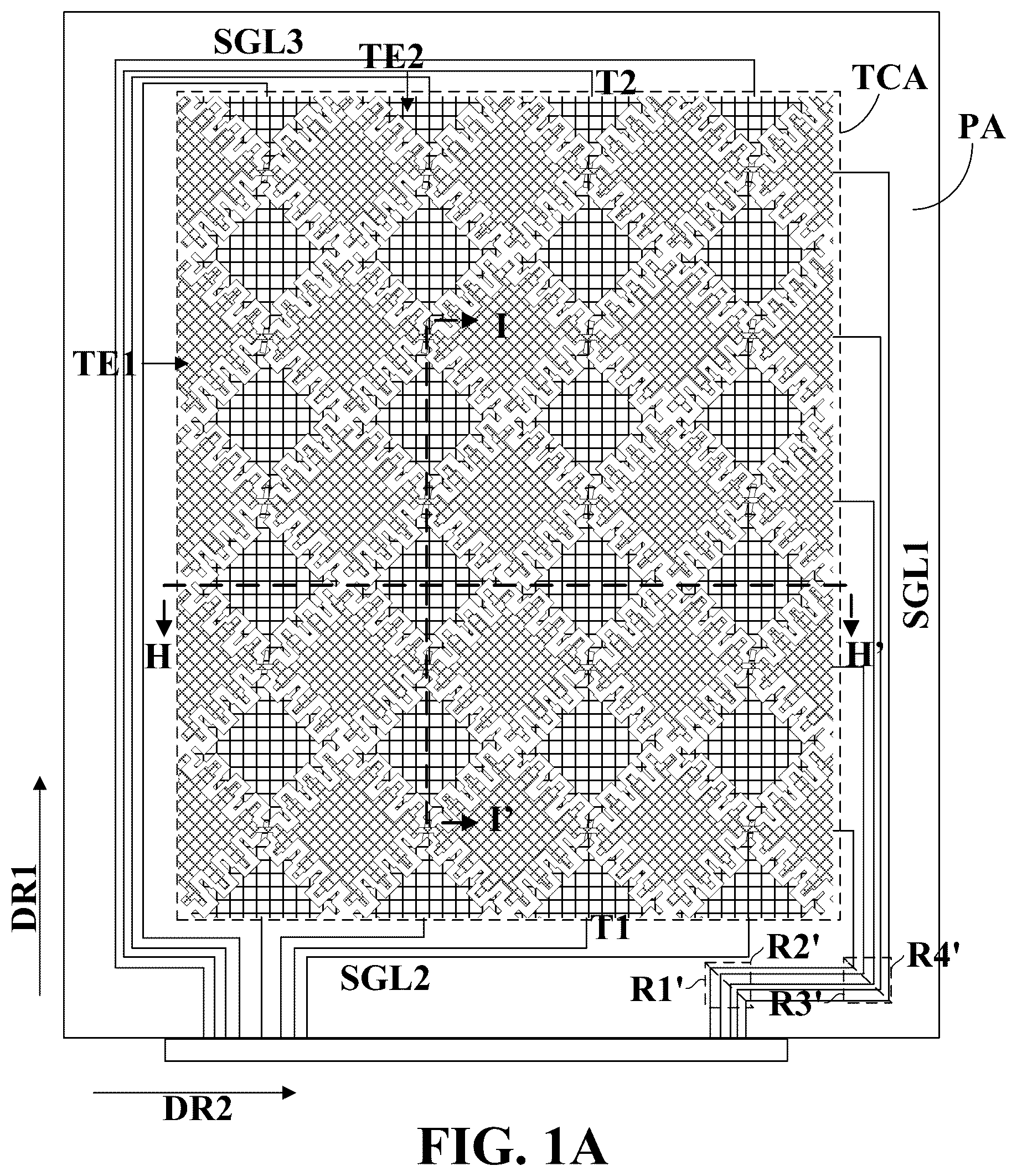
A is a schematic diagram illustrating the structure of a touch control structure in some embodiments according to the present disclosure. Referring to A , the touch control structure in some embodiments includes a plurality of first mesh electrodes TE 1 arranged in a plurality of rows and a plurality of second mesh electrodes TE 2 arranged in a plurality of columns. Adjacent rows of the plurality of rows are isolated from each other. Adjacent columns of the plurality of columns are isolated from each other. Optionally, the touch control structure is a mutual capacitance type touch control structure. Optionally, the plurality of first mesh electrodes TE 1 are a plurality of touch sensing electrodes, and the plurality of second mesh electrodes TE 2 are a plurality of touch scanning electrodes. Optionally, the plurality of first mesh electrodes TE 1 are a plurality of touch scanning electrodes, and the plurality of second mesh electrodes TE 2 are a plurality of touch sensing electrodes.
In some embodiments, the plurality of touch signal lines include a plurality of first touch signal lines SGL 1 respectively connected to the plurality of first mesh electrodes TE 1 ; a plurality of second touch signal lines SGL 2 respectively connected to first terminals T 1 of the plurality of second mesh electrodes TE 2 ; and a plurality of third touch signal lines SGL 3 respectively connected to second terminals T 2 of the plurality of second mesh electrodes TE 2 . Optionally, a respective one of the plurality of first mesh electrodes TE 1 to a respective one of the plurality of first touch signal lines SGL 1 . Optionally, a respective one of the plurality of second mesh electrodes TE 2 is connected to a respective one of the plurality of second touch signal lines SGL 2 , and connected to a respective one of the plurality of third touch signal lines SGL 3 .
In some embodiments, the respective one of the plurality of first mesh electrodes TE 1 extends along a second direction DR 2 ; and the respective one of the plurality of second mesh electrodes TE 2 extends along a first direction DR 1 . Optionally, the first direction DR 1 and the second direction DR 2 are two non-parallel directions, for example, the first direction DR 1 and the second direction DR 2 cross over each other. Optionally, the first direction DR 1 and the second direction DR 2 are perpendicular to each other. Optionally, the first direction DR 1 and the second direction DR 2 cross over each other at an inclined angle that is not 90 degrees.
In some embodiments, the plurality of touch electrodes (e.g., the plurality of first mesh electrodes TE 1 and the plurality of second mesh electrodes TE 2 ) are in a touch control area TCA, and the plurality of touch signal lines (e.g., the plurality of first touch signal lines SGL 1 , the plurality of second touch signal lines SGL 2 , and the plurality of third touch signal lines SGL 3 ) are in a peripheral area PA outside of the touch control area TCA.
B is a schematic diagram illustrating a touch control area and a peripheral area in a touch control structure in some embodiments according to the present disclosure. Referring to B , in some embodiments, the peripheral area PA includes a first sub-area PA 1 on a first side S 1 of the touch control area TCA, a second sub-area PA 2 on a second side S 2 of the touch control area TCA, a third sub-area PA 3 on a third side S 3 of the touch control area TCA, a fourth sub-area PA 4 on a fourth side S 4 of the touch control area TCA. Optionally, the first side S 1 and the fourth side S 4 are opposite to each other. Optionally, the second side S 2 and the third side S 3 are opposite to each other. Optionally, the first sub-area PA 1 is a sub-area where the plurality of first touch signal lines SGL 1 , the plurality of second touch signal lines SGL 2 , and the plurality of third touch signal lines SGL 3 are connected to an integrated circuit (e.g., an integrated touch control circuit).
In some embodiments, the first sub-area PA 1 includes a side region SR and one or more corner regions (e.g., a first corner region CR 1 and a second corner region CR 2 ). The one or more corner regions are respectively at a corner of the touch control structure. The one or more corner regions respectively connect the side region SR to one or more adjacent sub-areas of the peripheral area PA. For example, the first corner region CR 1 connects the side region SR to the second sub-area PA 2 , and the second corner region CR 2 connects the side region SR to the third sub-area PA 3 .
In some embodiments, the first sub-area PA 1 has a first shortest width w 1 along a direction from the touch control area TCA to the first sub-area PAL. Optionally, the second sub-area PA 2 has a second shortest width w 2 along a direction from the touch control area TCA to the second sub-area PA 2 . Optionally, the third sub-area PA 3 has a third shortest width w 3 along a direction from the touch control area TCA to the third sub-area PA 3 . Optionally, the fourth sub-area PA 4 has a fourth shortest width w 4 along a direction from the touch control area TCA to the fourth sub-area PA 4 . In some embodiments, the first shortest width w 1 is greater than at least one of the other shortest widths, e.g., greater than at least one of the second shortest width w 2 , the third shortest width w 3 , or the fourth shortest width w 4 . Optionally, the first shortest width w 1 is greater than any one of the other shortest widths, e.g., greater than the second shortest width w 2 , greater than the third shortest width w 3 , and greater than the fourth shortest width w 4 .
is a partial zoom-in view of a touch control structure in a region transition from a touch control area to a peripheral area in some embodiments according to the present disclosure. Referring to , the touch control structure in some embodiments includes a plurality of touch signal lines. A respective one of the plurality of touch signal lines in some embodiments includes a double-layer structure DLS in a double-layer region DLR and a single-layer structure SLS in a single-layer region SLR. The double-layer region DLR and the single-layer region SLR are in the peripheral area of the touch control structure. In some embodiments, the double-layer region DLR and the single-layer region SLR are in the first sub-area PAL.
In some embodiments, the touch control structure includes a plurality of adjacent double-layer structures and a plurality of adjacent single-layer structures. In some embodiments, at least two of the plurality of adjacent single-layer structures are respectively in a first layer and a second layer. A is a further zoom-in view of a zoom-in region in . B is a cross-sectional view along an A-A′ line in A . C is a cross-sectional view along a B-B′ line in A . D is a cross-sectional view along a C-C′ line in A . Referring to , A to D , a plurality of adjacent double-layer structures ADLS in the double-layer region DLR are respectively connected to a plurality of adjacent single-layer structures ASLS in the single-layer region SLR. Referring to A to D , in some embodiments, at least two of the plurality of adjacent single-layer structures are respectively in a first layer SL 1 and a second layer SL 2 . In one example depicted in A to D , the plurality of adjacent single-layer structures ASLS are alternately in a first layer SL 1 and a second layer SL 2 . In the context of the present disclosure, the plurality of adjacent single-layer structures ASLS are portions of touch signal lines. For example, referring to A , , A to D , at least two adjacent single-layer structures respectively in the first layer SL 1 and the second layer SL 2 are electrically connected to adjacent rows of touch electrodes.
In one example as shown in A to C , the touch control structure includes a buffer layer BUF on a second inorganic encapsulating sub-layer CVD 2 , the second inorganic encapsulating sub-layer CVD 2 being a sub-layer of an encapsulating layer for encapsulating light emitting elements in a display apparatus having the touch control structure. In some embodiments, the touch control structure further includes a first layer SL 1 on a side of the buffer layer BUF away from the second inorganic encapsulating sub-layer CVD 2 , a touch insulating layer TI on a side of the first layer SL 1 away from the buffer layer BUF, a second layer SL 2 on a side of the touch insulating layer TI away from the first layer SL 1 , and an overcoat layer OC on a side of the second layer SL 2 away from the touch insulating layer TI.
In some embodiments, a respective double-layer structure includes a first portion P 1 in the first layer SL 1 and a second portion P 2 in the second layer SL 2 , as depicted in A to C . As shown in B , a first adjacent respective single-layer structure ASLS 1 in the second layer SL 2 is connected to a respective second portion P 2 of a first adjacent double-layer structure ADLS 1 . A second adjacent respective single-layer structure ASLS 2 in the first layer SL 1 is connected to a respective first portion P 1 of a second adjacent double-layer structure ADLS 2 . Optionally, the first adjacent respective single-layer structure ASLS 1 in the second layer SL 2 is continuously connected to the respective second portion P 2 of a first adjacent double-layer structure ADLS 1 , forming a unitary structure. Optionally, the second adjacent respective single-layer structure ASLS 2 in the first layer SL 1 is continuously connected to the respective first portion P 1 of a second adjacent double-layer structure ADLS 2 , forming a unitary structure.
Referring to and D , in some embodiments, at least two of the plurality of adjacent single-layer structures ASLS are respectively in a first layer SL 1 and a second layer SL 2 . In one example depicted in and D , the plurality of adjacent single-layer structures ASLS are alternately in a first layer SL 1 and a second layer SL 2 . The inventors of the present disclosure discover that by having this structure, a pitch of the plurality of touch signal lines can be significantly decreased, a display apparatus having the present touch structure can be made to have a much narrower peripheral area. In one example, a width of a peripheral area from a display area to an edge of the display panel can be reduced from 1.36 mm to 1.076 mm. In another example, a distance between the display area and a signal line more distant to the display area can be reduced from 0.435 mm to 0.331 mm. Moreover, the signal lines in a same layer, for example, single-layer structures in the first layer SL 1 can be further spaced apart from each other, avoiding short. By having the single-layer structures in a same layer spaced apart further, it also reduces the complication involved in making a mask plate for patterning of the plurality of signal lines, and makes the etching process less prone to defects.
For example, the first sub-area of the peripheral area having the double-layer region and the single-layer region discussed above has a first shortest width along a direction from the touch control area to the first sub-area. The first shortest width can be reduced from 1.36 mm to 1.076 mm. The reference value 1.36 mm may be a reference first shortest width of a corresponding first sub-area of the peripheral area in a reference touch control structure that does not have the double-layer region and the single-layer region of the present disclosure. In one example, touch signal lines of the reference touch control structure adopt a double-layer structure throughout the peripheral area. By forming the touch signal lines to have an intricate structure as discussed in the present disclosure, the first shortest width in the first sub-area can be reduced as compared to that in the reference touch control structure.
For example, normally a minimum pitch of 7.5 μm is required to avoid defects such as short and etching defects. By having the plurality of adjacent single-layer structures ASLS alternately disposed in the first layer SL 1 and the second layer SL 2 , a minimum pitch can be significantly reduced to 5.6 μm or less. Further, signal lines in a same layer can be spaced apart, for example, from 7.5 μm to 11.2 μm or more.
In some embodiments, the respective one of the plurality of touch signal lines has a line width in a range of 2.5 μm to 4.5 μm, e.g., 2.5 μm to 3.0 μm, 3.0 μm to 3.5 μm, 3.5 μm to 4.0 μm, or 4.0 μm to 4.5 μm. Optionally, the respective one of the plurality of touch signal lines has a line width of 3.5 μm. In some embodiments, the plurality of adjacent single-layer structures ASLS has a line width (denoted as lw in D ) in a range of 2.5 μm to 4.5 μm, e.g., 2.5 μm to 3.0 μm, 3.0 μm to 3.5 μm, 3.5 μm to 4.0 μm, or 4.0 μm to 4.5 μm. Optionally, the plurality of adjacent single-layer structures ASLS has a line width of 3.5 μm. In some embodiments, the plurality of adjacent double-layer structures ADLS has a line width in a range of 2.5 μm to 4.5 μm, e.g., 2.5 μm to 3.0 μm, 3.0 μm to 3.5 μm, 3.5 μm to 4.0 μm, or 4.0 μm to 4.5 μm. Optionally, the plurality of adjacent double-layer structures ADLS has a line width of 3.5 μm.
Referring to D , in some embodiments, orthographic projections of adjacent single-layer structures on a base substrate are spaced apart by a shortest distance d in a range of 1.1 μm to 3.1 μm, e.g., 1.1 μm to 1.6 μm, 1.6 μm to 2.1 μm, or 2.6 μm to 3.1 μm. Optionally, the orthographic projections of adjacent single-layer structures on a base substrate are spaced apart by a shortest distance of 2.1 μm. In some embodiments, orthographic projections of adjacent single-layer structures in the first layer SL 1 on the base substrate are spaced apart by a shortest distance d 1 in a range of 4.7 μm to 10.7 μm, e.g., 4.7 μm to 5.7 μm, 5.7 μm to 6.7 μm, 6.7 μm to 7.7 μm, 7.7 μm to 8.7 μm, 8.7 μm to 9.7 μm, or 9.7 μm to 10.7 μm. Optionally, the orthographic projections of adjacent single-layer structures in the first layer SL 1 on the base substrate are spaced apart by a shortest distance of 7.7 μm. In some embodiments, orthographic projections of adjacent single-layer structures in the second layer SL 2 on the base substrate are spaced apart by a shortest distance d 2 in a range of 4.7 μm to 10.7 μm, e.g., 4.7 μm to 5.7 μm, 5.7 μm to 6.7 μm, 6.7 μm to 7.7 μm, 7.7 μm to 8.7 μm, 8.7 μm to 9.7 μm, or 9.7 μm to 10.7 μm. Optionally, the orthographic projections of adjacent single-layer structures in the second layer SL 2 on the base substrate are spaced apart by a shortest distance of 7.7 μm.
Referring to D , Optionally, orthographic projections of adjacent single-layer structures in the first layer SL 1 and the second layer SL 2 are non-overlapping with each other.
E is a cross-sectional view of a plurality of adjacent single-layer structures ASLS in the single-layer region in some embodiments according to the present disclosure. Referring to E , in some embodiments, orthographic projections of adjacent single-layer structures of the plurality of adjacent single-layer structures ASLS on a base substrate directly abutting each other.
F is a cross-sectional view of a plurality of adjacent single-layer structures ASLS in the single-layer region in some embodiments according to the present disclosure. Referring to F , in some embodiments, orthographic projections of adjacent single-layer structures of the plurality of adjacent single-layer structures ASLS on a base substrate at least partially overlapping with each other.
Referring to A to C , in some embodiments, the first portion P 1 and the second portion P 2 of a respective double-layer structure are connected through a connecting via cv extending through the touch insulating layer TI.
In some embodiments, orthographic projections of adjacent double-layer structures on a base substrate are spaced apart by a shortest distance d in a range of 3.0 μm to 5.0 μm, e.g., 3.0 μm to 3.5 μm, 3.5 μm to 4.0 μm, 4.0 μm to 4.5 μm, or 4.5 μm to 5.0 μm. Optionally, the orthographic projections of adjacent double-layer structures on a base substrate are spaced apart by a shortest distance of 4.0 μm.
is a partial zoom-in view of a touch control structure in a region transition from a touch control area to a peripheral area in some embodiments according to the present disclosure. is a further zoom-in view of a first zoom-in region in . Referring to and , in some embodiments, multiple first double-layer structures MDLS 1 respectively of multiple touch signal lines of the plurality of touch signal lines are clustered in a first region R 1 ; and multiple first single-layer structures MSLS 1 respectively of the multiple touch signal lines of the plurality of touch signal lines are clustered in a second region R 2 . The multiple first double-layer structures MDLS 1 are respectively connected to the multiple first single-layer structures MSLS 1 (as similarly discussed in connection with , A to B ). The first region R 1 and the second region R 2 are directly adjacent to each other.
In some embodiments, the multiple first double-layer structures MDLS 1 and the multiple first single-layer structures MSLS 1 are portions of touch signal lines of a same type. In one example, the multiple first double-layer structures MDLS 1 and the multiple first single-layer structures MSLS 1 are portions of touch scanning signal lines connected to touch scanning electrodes. In another example, the multiple first double-layer structures MDLS 1 and the multiple first single-layer structures MSLS 1 are portions of touch sensing signal lines connected to touch sensing electrodes. In one example, the multiple first double-layer structures MDLS 1 and the multiple first single-layer structures MSLS 1 are portions of the plurality of first touch signal lines SGL 1 . The regions corresponding to the first region R 1 and the second region R 2 are denoted as R 1 ′ and R 2 ′ in A .
In some embodiments, multiple connecting points CP 3 respectively connecting the multiple first double-layer structures MDLS 1 and the multiple first single-layer structures MSLS 1 are arranged along a seventh direction DR 7 . Optionally, the second direction DR 2 and the seventh direction DR 7 are two non-parallel directions, for example, the second direction DR 2 and the seventh direction DR 7 cross over each other. Optionally, the second direction DR 2 and the seventh direction DR 7 cross over each other at an inclined angle that is not 90 degrees. In some embodiments, the second direction DR 2 and the seventh direction DR 7 intersect each other at an angle in a range of 6 degrees to 15 degrees, e.g., 6 degrees to 7 degrees, 7 degrees to 8 degrees, 8 degrees to 9 degrees, 9 degrees to 10 degrees, 10 degrees to 11 degrees, 11 degrees to 12 degrees, 12 degrees to 13 degrees, 13 degrees to 14 degrees, or 14 degrees to 15 degrees. Optionally, the second direction DR 2 and the seventh direction DR 7 intersect each other at an angle of 10.5 degrees.
is a cross-sectional view along a D-D′ line in . Referring to , and as similarly discussed above in connection with A to D , in some embodiments, in the second region R 2 , at least two of the multiple first single-layer structures MSLS 1 are respectively in the first layer SL 1 and the second layer SL 2 . In one example as depicted in , A to D , in the second region R 2 , the multiple first single-layer structures MSLS 1 are alternately in the first layer SL 1 and the second layer SL 2 .
In some embodiments, the multiple first double-layer structures MDLS 1 are substantially parallel to each other, and respectively extend along a first direction DR 1 ; and the multiple first single-layer structures MSLS 1 are substantially parallel to each other, and respectively extend along a second direction DR 2 . The first direction DR 1 and the second direction DR 2 are different from each other, and intersecting each other at an angle greater than zero. Optionally, the first direction DR 1 and the second direction DR 2 are two non-parallel directions, for example, the first direction DR 1 and the second direction DR 2 cross over each other. Optionally, the first direction DR 1 and the second direction DR 2 are perpendicular to each other. Optionally, the first direction DR 1 and the second direction DR 2 cross over each other at an inclined angle that is not 90 degrees.
is a further zoom-in view of a second zoom-in region in . Referring to and , in some embodiments, multiple first single-layer structures MSLS 1 respectively of the multiple touch signal lines of the plurality of touch signal lines are clustered in a second region R 2 ; and multiple second single-layer structures MSLS 2 respectively of the multiple touch signal lines of the plurality of touch signal lines are clustered in a third region R 3 . The multiple first single-layer structures MSLS 1 are respectively connected to the multiple second single-layer structures MSLS 2 . The second region R 2 and the third region R 3 are directly adjacent to each other.
In some embodiments, the multiple first single-layer structures MSLS 1 and the multiple second single-layer structures MSLS 2 are portions of touch signal lines of a same type. In one example, the multiple first single-layer structures MSLS 1 and the multiple second single-layer structures MSLS 2 are portions of touch scanning signal lines connected to touch scanning electrodes. In another example, the multiple first single-layer structures MSLS 1 and the multiple second single-layer structures MSLS 2 are portions of touch sensing signal lines connected to touch sensing electrodes. In one example, the multiple first single-layer structures MSLS 1 and the multiple second single-layer structures MSLS 2 are portions of the plurality of first touch signal lines SGL 1 . In one example, the multiple first single-layer structures MSLS 1 and the multiple second single-layer structures MSLS 2 are portions of the plurality of second touch signal lines SGL 2 . In one example, the multiple first single-layer structures MSLS 1 and the multiple second single-layer structures MSLS 2 are portions of the plurality of third touch signal lines SGL 3 .
In some embodiments, the multiple first single-layer structures MSLS 1 are substantially parallel to each other, and respectively extend along a second direction DR 2 ; and the multiple second single-layer structures MSLS 2 are substantially parallel to each other, and respectively extend along a third direction DR 3 . Optionally, the second direction DR 2 and the third direction DR 3 are two non-parallel directions, for example, the second direction DR 2 and the third direction DR 3 cross over each other. Optionally, the second direction DR 2 and the third direction DR 3 cross over each other at an inclined angle that is not 90 degrees. In some embodiments, the second direction DR 2 and the third direction DR 3 intersect each other at an angle in a range of 15 degrees to 25 degrees, e.g., 15 degrees to 17 degrees, 17 degrees to 19 degrees, 19 degrees to 21 degrees, 21 degrees to 23 degrees, or 23 degrees to 25 degrees. Optionally, the second direction DR 2 and the third direction DR 3 intersect each other at an angle of 20.03 degrees.
is a cross-sectional view along an E-E′ line in . Referring to , in some embodiments, in the second region R 2 , at least two of the multiple first single-layer structures MSLS 1 are respectively in the first layer SL 1 and the second layer SL 2 . In one example as depicted in and , in the second region R 2 , the multiple first single-layer structures MSLS 1 are alternately in the first layer SL 1 and the second layer SL 2 . In some embodiments, in the third region R 3 , at least two of the multiple second single-layer structures MSLS 2 are respectively in the first layer SL 1 and the second layer SL 2 . In one example as depicted in and , in the third region R 3 , the multiple second single-layer structures MSLS 2 are alternately in the first layer SL 1 and the second layer SL 2 .
In some embodiments, multiple connecting points CP 1 respectively connecting the multiple first single-layer structures MSLS 1 and the multiple second single-layer structures MSLS 2 are arranged along a fourth direction DR 4 . Optionally, the second direction DR 2 and the fourth direction DR 4 are two non-parallel directions, for example, the second direction DR 2 and the fourth direction DR 4 cross over each other. Optionally, the second direction DR 2 and the fourth direction DR 4 cross over each other at an inclined angle that is not 90 degrees. In some embodiments, the second direction DR 2 and the fourth direction DR 4 intersect each other at an angle in a range of 20 degrees to 40 degrees, e.g., 20 degrees to 25 degrees, 25 degrees to 30 degrees, 30 degrees to 35 degrees, or 35 degrees to 40 degrees. Optionally, the second direction DR 2 and the fourth direction DR 4 intersect each other at an angle of 30.848 degrees.
In some embodiments, referring to , , and , multiple second single-layer structures MSLS 2 respectively of the multiple touch signal lines of the plurality of touch signal lines are clustered in a third region R 3 ; and multiple second double-layer structures MDLS 2 respectively of the multiple touch signal lines of the plurality of touch signal lines are clustered in a fourth region R 4 . The multiple second single-layer structures MSLS 2 are respectively connected to the multiple second double-layer structures MDLS 2 . The third region R 3 and the fourth region R 4 are directly adjacent to each other. Optionally, the third region R 3 and the fourth region R 4 are in a corner region of the touch control structure. For example, the regions corresponding to the third region R 3 and the fourth region R 4 are denoted as R 3 ′ and R 4 ′ in A .
In some embodiments, the multiple second single-layer structures MSLS 2 and the multiple second double-layer structures MDLS 2 are portions of touch signal lines of a same type. In one example, the multiple second single-layer structures MSLS 2 and the multiple second double-layer structures MDLS 2 are portions of touch scanning signal lines connected to touch scanning electrodes. In another example, the multiple second single-layer structures MSLS 2 and the multiple second double-layer structures MDLS 2 are portions of touch sensing signal lines connected to touch sensing electrodes. In one example, the multiple second single-layer structures MSLS 2 and the multiple second double-layer structures MDLS 2 are portions of the plurality of first touch signal lines SGL 1 . In one example, the multiple second single-layer structures MSLS 2 and the multiple second double-layer structures MDLS 2 are portions of the plurality of second touch signal lines SGL 2 . In one example, the multiple second single-layer structures MSLS 2 and the multiple second double-layer structures MDLS 2 are portions of the plurality of third touch signal lines SGL 3 .
In some embodiments, the multiple second single-layer structures MSLS 2 are substantially parallel to each other, and respectively extend along a third direction DR 3 ; and the multiple second double-layer structures MDLS 2 are substantially parallel to each other, and respectively extend along a fifth direction DR 5 .
In some embodiments, the third direction DR 3 and the fifth direction DR 5 are substantially parallel to each other, e.g., within an error of less than 5 degrees, or perfectly parallel to each other.
In some embodiments, the third direction DR 3 and the fifth direction DR 5 are two non-parallel directions, for example, the third direction DR 3 and the fifth direction DR 5 cross over each other. Optionally, the third direction DR 3 and the fifth direction DR 5 cross over each other at an inclined angle that is not 90 degrees. In some embodiments, the third direction DR 3 and the fifth direction DR 5 intersect each other at an angle less than 10 degrees.
Referring to , in some embodiments, in the third region R 3 , the multiple second single-layer structures MSLS 2 are alternately in the first layer SL 1 and the second layer SL 2 .
In some embodiments, multiple second connecting points CP 2 respectively connecting the multiple second single-layer structures MSLS 2 and the multiple second double-layer structures MDLS 2 are arranged along a sixth direction DR 6 .
In some embodiments, the second direction DR 2 and the sixth direction DR 6 are substantially parallel to each other, e.g., within an error of less than 5 degrees, or perfectly parallel to each other.
In some embodiments, the second direction DR 2 and the sixth direction DR 6 are two non-parallel directions, for example, the second direction DR 2 and the sixth direction DR 6 cross over each other. Optionally, the second direction DR 2 and the sixth direction DR 6 cross over each other at an inclined angle that is not 90 degrees. In some embodiments, the second direction DR 2 and the sixth direction DR 6 intersect each other at an angle less than 10 degrees.
is a cross-sectional view along an F-F′ line in . Referring to and , the touch control structure in some embodiments includes a via v extending through the touch insulating layer TI at a respective second connecting point CP 2 , a material in the second layer SL 2 connected to a material in the first layer SL 1 through the via v.
is a partial zoom-in view of a touch control structure in a region transition from a touch control area to a peripheral area in some embodiments according to the present disclosure. is a further zoom-in view of . Referring to and , multiple third double-layer structures MDLS 3 respectively of multiple touch signal lines of the plurality of touch signal lines are clustered in a fifth region R 5 ; multiple fourth double-layer structures MDLS 4 respectively of the multiple touch signal lines of the plurality of touch signal lines are clustered in a sixth region R 6 ; multiple third single-layer structures MSLS 3 respectively of the multiple touch signal lines of the plurality of touch signal lines are clustered in a seventh region R 7 . The multiple fourth double-layer structures MDLS 4 in the sixth regions R 6 are respectively connected to the multiple third single-layer structures MSLS 3 in the seventh region R 7 . The multiple third single-layer structures MSLS 3 in the seventh region R 7 are respectively connected to the multiple third double-layer structures MDLS 3 in the fifth region R 5 . The sixth regions R 6 is directly adjacent to the seventh region R 7 . The seventh region R 7 is directly adjacent to the fifth region R 5 .
In some embodiments, the multiple third double-layer structures MDLS 3 , the multiple fourth double-layer structures MDLS 4 , and the multiple third single-layer structures MSLS 3 are portions of touch signal lines of a same type. In one example, the multiple third double-layer structures MDLS 3 , the multiple fourth double-layer structures MDLS 4 , and the multiple third single-layer structures MSLS 3 are portions of touch scanning signal lines connected to touch scanning electrodes. In another example, the multiple third double-layer structures MDLS 3 , the multiple fourth double-layer structures MDLS 4 , and the multiple third single-layer structures MSLS 3 are portions of touch sensing signal lines connected to touch sensing electrodes. In one example, the multiple third double-layer structures MDLS 3 , the multiple fourth double-layer structures MDLS 4 , and the multiple third single-layer structures MSLS 3 are portions of the plurality of first touch signal lines SGL 1 . In one example, the multiple third double-layer structures MDLS 3 , the multiple fourth double-layer structures MDLS 4 , and the multiple third single-layer structures MSLS 3 are portions of the plurality of second touch signal lines SGL 2 . In one example, the multiple third double-layer structures MDLS 3 , the multiple fourth double-layer structures MDLS 4 , and the multiple third single-layer structures MSLS 3 are portions of the plurality of third touch signal lines SGL 3 .
illustrates a respective one of multiple third single-layer structures connecting a respective one of multiple third double-layer structures and a respective one of multiple fourth double-layer structures. Referring to , a respective one of the multiple third single-layer structures MSLS 3 is a half loop structure connecting a respective one of the multiple third double-layer structures MDLS 3 and a respective one of the multiple fourth double-layer structures MDLS 4 . The half loop structure includes two parallel portions PP 1 and PP 2 respectively extending along a second direction DR 2 and a connecting portion CPP connecting the two parallel portions PP 1 and PP 2 together.
In some embodiments, the multiple third double-layer structures MDLS 3 are substantially parallel to each other, and respectively extend along a first direction DR 1 ; and the multiple fourth double-layer structures MDLS 4 are substantially parallel to each other, and respectively extend along the first direction DR 1 . The first direction DR 1 and the second direction DR 2 are different from each other, and intersecting each other at an angle greater than zero. Optionally, the first direction DR 1 and the second direction DR 2 are two non-parallel directions, for example, the first direction DR 1 and the second direction DR 2 cross over each other. Optionally, the first direction DR 1 and the second direction DR 2 are perpendicular to each other. Optionally, the first direction DR 1 and the second direction DR 2 cross over each other at an inclined angle that is not 90 degrees.
is a cross-sectional view along a G-G′ line in . Referring to and , in some embodiments, in the seventh region R 7 , at least two of the multiple third single-layer structures MSLS 3 are respectively in the first layer SL 1 and the second layer SL 2 . In one example as depicted in and , in the seventh region R 7 , the multiple third single-layer structures MSLS 3 are alternately in the first layer SL 1 and the second layer SL 2 .
Referring to and , in some embodiments, multiple fourth single-layer structures MSLS 4 respectively of the multiple touch signal lines of the plurality of touch signal lines are clustered in an eighth region R 8 . The multiple fourth single-layer structures MSLS 4 are substantially parallel to each other, and respectively extend along the second direction DR 2 . The multiple fourth single-layer structures MSLS 4 are respectively connected to the multiple third double-layer structures MDLS 3 . As shown in , , , and , the multiple fourth single-layer structures MSLS 4 are at least a sub-set of multiple first single-layer structures MSLS 1 .
is a cross-sectional view along an H-H′ line in A . is a cross-sectional view along an I-I′ line in A . As shown in A , , and , in some embodiments, the touch control structure includes a plurality of first mesh electrodes TE 1 arranged in a plurality of rows and a plurality of second mesh electrodes TE 2 arranged in a plurality of columns. The plurality of first mesh electrodes TE 1 and the plurality of second mesh electrodes TE 2 are in the second layer SL 2 . The touch control structure further includes a plurality of touch electrode bridges EB in the first layer SL 1 ; and vias Vb extending through the touch insulating layer TI. Optionally, the plurality of touch electrode bridges EB respectively extend through the vias Vb to respectively connect adjacent second mesh blocks in a respective column of the plurality of column of the plurality of second mesh electrodes TE 2 .
is a schematic diagram illustrating a touch control structure in some embodiments according to the present disclosure. Referring to , the touch control structure in some embodiments includes a plurality of first mesh electrodes TE 1 and a plurality of second mesh electrodes TE 2 . Optionally, the touch control structure is a mutual capacitance type touch control structure. Optionally, the plurality of first mesh electrodes TE 1 are a plurality of touch scanning electrodes, and the plurality of second mesh electrodes TE 2 are a plurality of touch sensing electrodes. Optionally, the plurality of mesh touch electrodes TE 1 are a plurality of touch sensing electrodes, and the plurality of second mesh electrodes TE 2 are a plurality of touch scanning electrodes. The touch control structure is limited in a touch control region TCR and absent in a window region WR surrounded by the touch control region TCR. For example, the touch control structure may be a touch control structure in a display panel, where the touch control region TCR substantially overlaps with a display region of the display panel, and the window region WR is a region in the display panel having a hole configured for installing an accessory such as a camera lens or a fingerprint sensor. The display panel is configured to display an image in at least a portion of the touch control region TCR. In one example, in the window region WR, display elements of the display panel and the touch control structure are absent; in the display region or at least a portion of the touch control region TCR, both display elements of the display panel and the touch control structure are present.
Referring to , in some embodiments, the plurality of mesh touch electrodes TE 1 are arranged in a plurality of rows, each of which is a respective one of the plurality of mesh touch electrodes TE 1 ; the plurality of mesh scanning electrodes TE 2 are arranged in a plurality of columns, each of which is a respective one of the plurality of second mesh electrodes TE 2 . In some embodiments, at least one row of the plurality of rows of first mesh electrodes TE 1 crosses over the window region WR. For example, as shown in , a window-crossing row Rwc of the plurality of first mesh electrodes TE 1 crosses over the window region WR. The touch electrode in the window-crossing row Rwc is spaced apart by the window region WR into two portions (a portion on left side of the window region WR and a portion on right side of the window region WR). In some embodiments, at least one column of the plurality of columns of second mesh electrodes TE 2 crosses over the window region WR. For example, as shown in , a window-crossing column Cwc of the plurality of second mesh electrodes TE 2 crosses over the window region WR. The touch electrode in the window-crossing column Cwc is spaced apart by the window region WR into two portions (a portion on upper side of the window region WR and a portion on lower side of the window region WR).
A is a schematic diagram illustrating a window region in some embodiments according to the present disclosure. B is a zoom-in view of a touch control structure surrounding a window region in some embodiments according to the present disclosure. C is a further zoom-in view of a touch control structure surrounding a window region in some embodiments according to the present disclosure. Referring to A , in some embodiments, the window region WR has at least four sides, including a first side S 1 , a second side S 2 , a third side S 3 , and a fourth side S 4 . Referring to A to C , in some embodiments, the window-crossing row Rwc of the plurality of first mesh electrodes TE 1 includes a first mesh block MB 1 and a second mesh block MB 2 respectively on a first side S 1 and a second side S 2 of the window region WR; a first conductive plate CP 1 directly connected to multiple mesh lines of the first mesh block MB 1 ; a second conductive plate CP 2 directly connected to multiple mesh lines of the second mesh block MB 2 ; and a first conductive bridge CB 1 connecting the first conductive plate CP 1 and the second conductive plate CP 2 .
In the present touch control structure, the adjacent mesh blocks (e.g., the first mesh block MB 1 and the second mesh block MB 2 ) separated by the window region WR are connected by a conductive connecting bridge (e.g., the first conductive bridge CB 1 ) through the aid of conductive plates (e.g., the first conductive plate CP 1 and the second conductive plate CP 2 ). Because forming the connecting bridge typically involves forming vias to connect corresponding mesh electrodes, it is extremely difficult to precisely connect mesh electrode lines with the connecting bridge without a conductive plate as an intermediate. The novel and unique structure of the present touch control structure ensures the adjacent mesh blocks separated by the window region WR are connected to transmit touch signals.
Referring to A and C , the first conductive plate CP 1 , the second conductive plate CP 2 , and the first conductive bridge CB 1 are respectively around a first portion P 1 , a second portion P 2 , and a third portion P 3 of a periphery of the window region WR. Optionally, the third portion P 3 is partially overlapping with the first portion P 1 , and partially overlapping with the second portion P 2 . Optionally, the first portion P 1 is on the first side S 1 of the window region WR; the second portion P 2 is on the second side S 2 of the window region WR; and the third portion P 3 is on the fourth side S 4 of the window region WR.
Referring to A to C , in some embodiments, the window-crossing column Cwc of the plurality of second mesh electrodes TE 2 includes a third mesh block MB 3 and a fourth mesh block MB 4 respectively on a third side S 3 and a fourth side S 4 of the window region WR; a third conductive plate CP 3 directly connected to multiple mesh lines of the third mesh block MB 3 ; a fourth conductive plate CP 4 directly connected to multiple mesh lines of the fourth mesh block MB 4 ; and a second conductive bridge CB 2 connecting the third conductive plate CP 3 and the fourth conductive plate CP 4 .
Referring to A and C , the third conductive plate CP 3 , the fourth conductive plate CP 4 , and the second conductive bridge CB 2 are respectively around a fourth portion P 4 , a fifth portion P 5 , and a sixth portion P 6 of the periphery of the window region WR. In one example, the third conductive plate CP 3 , the fourth conductive plate CP 4 , and the second conductive bridge CB 2 are parts of a unitary structure; the third conductive plate CP 3 include a plate of a first arch shape, the fourth conductive plate CP 4 include a plate of a second arch shape, and the second conductive bridge CB 2 include a bridge of a third arch shape. In another example, the third arch shape is non-concentric with respect to the first arch shape, and is non-concentric with respect to the second arch shape, thus the boundary between the third conductive plate CP 3 and the second conductive bridge CB 2 and boundary between the fourth conductive plate CP 4 and the second conductive bridge CB 2 can be discerned. In another example, the third arch shape has a radius different from that of the first arch shape, and different from that of the second arch shape, thus the boundary between the third conductive plate CP 3 and the second conductive bridge CB 2 and boundary between the fourth conductive plate CP 4 and the second conductive bridge CB 2 can be discerned. Optionally, the sixth portion P 6 is partially overlapping with the fourth portion P 4 , and partially overlapping with the fifth portion P 5 . Optionally, the fourth portion P 4 is on the third side S 3 of the window region WR; the fifth portion P 5 is on the fourth side S 4 of the window region WR; and the sixth portion P 6 is on the second side S 2 of the window region WR.
Referring to A to C , in some embodiments, the window-crossing row Rwc of the plurality of first mesh electrodes TE 1 further includes a third conductive bridge CB 3 connecting the first conductive plate CP 1 and the second conductive plate CP 2 . Referring to A and C , the first conductive plate CP 1 , the second conductive plate CP 2 , and the third conductive bridge CB 3 are respectively around a first portion P 1 , a second portion P 2 , and a seventh portion P 7 of a periphery of the window region WR. Optionally, the seventh portion P 7 is partially overlapping with the first portion P 1 , and partially overlapping with the second portion P 2 . Optionally, the first portion P 1 is on the first side S 1 of the window region WR; the second portion P 2 is on the second side S 2 of the window region WR; and the seventh portion P 7 is on the third side S 3 of the window region WR.
Referring to A to C , in some embodiments, the window-crossing column Cwc of the plurality of second mesh electrodes TE 2 further includes a fourth conductive bridge CB 4 connecting the third conductive plate CP 3 and the fourth conductive plate CP 4 . Referring to A and C , the third conductive plate CP 3 , the fourth conductive plate CP 4 , and the fourth conductive bridge CB 4 are respectively around a fourth portion P 4 , a fifth portion P 5 , and an eighth portion P 8 of the periphery of the window region WR. Optionally, the eighth portion P 8 is partially overlapping with the fourth portion P 4 , and partially overlapping with the fifth portion P 5 . Optionally, the fourth portion P 4 is on the third side S 3 of the window region WR; the fifth portion P 5 is on the fourth side S 4 of the window region WR; and the eighth portion P 8 is on the first side S 1 of the window region WR.
Referring to , in some embodiments, the window-crossing row Rwc further includes a plurality of first non-window mesh blocks NWB 1 , and the window-crossing column Cwc further includes a plurality of second non-window mesh blocks NWB 2 . Optionally, at least the first mesh block MB 1 has an area smaller than (by 5%, by 10%, by 20%, by 30%, by 40%, by 50%, by 60%, by 70%, by 80%, by 90%, or by 95% or more) each of the plurality of first non-window mesh blocks NWB 1 due to presence of the window region WR. Optionally, the first mesh block MB 1 has an area smaller than each of the plurality of first non-window mesh blocks NWB 1 , and the second mesh block MB 2 also has an area smaller than each of the plurality of first non-window mesh blocks NWB 1 . Optionally, at least the third mesh block MB 3 has an area smaller than each of the plurality of second non-window mesh blocks NWB 2 due to presence of the window region WR. Optionally, the third mesh block MB 3 has an area smaller than each of the plurality of second non-window mesh blocks NWB 2 , and the fourth mesh block MB 4 also has an area smaller than each of the plurality of second non-window mesh blocks NWB 2 .
In another aspect, the present disclosure provides a display apparatus. In some embodiments, the display apparatus includes a display panel; a touch control structure described herein or fabricated by a method described herein; and an integrated circuit. Examples of appropriate display apparatuses include, but are not limited to, an electronic paper, a mobile phone, a tablet computer, a television, a monitor, a notebook computer, a digital album, a GPS, etc. Optionally, the display apparatus is an organic light emitting diode display apparatus. Optionally, the display apparatus is a liquid crystal display apparatus.
is a cross sectional view of a display panel in some embodiments according to the present disclosure. Referring to , in the display region, the display panel includes a base substrate BS, a plurality of thin film transistors TFT on the base substrate BS, a passivation layer PVX on a side of the plurality of thin film transistors TFT away from the base substrate BS, a first planarization layer PLN 1 on side of the passivation layer PVX away from the base substrate BS, a relay electrode RE on side of the first planarization layer PLN 1 away from the passivation layer PVX, a second planarization layer PLN 2 on a side of the relay electrode RE away from the first planarization layer PLN 1 , a pixel definition layer PDL on a side of the second planarization layer PLN 2 away from the first planarization layer PLN 1 and defining subpixel apertures, an anode AD on a side of the second planarization layer PLN 2 away from the first planarization layer PLN 1 , a light emitting layer EL on a side of the anode AD away from the second planarization layer PLN 2 , a cathode CD on a side of the light emitting layer EL away from the anode AD, a first inorganic encapsulating layer CVD 1 on a side of the cathode CD away from light emitting layer EL, an organic encapsulating layer IJP on a side of the first inorganic encapsulating layer CVD 1 away from the cathode CD, a second inorganic encapsulating layer CVD 2 on a side of the organic encapsulating layer IJP away from the first inorganic encapsulating layer CVD 1 , a buffer layer BUF on a side of the second inorganic encapsulating layer CVD 2 away from the organic encapsulating layer IJP, a touch insulating layer TI on a side of the buffer layer BUF away from the second inorganic encapsulating layer CVD 2 , touch electrodes (e.g., the plurality of first touch electrodes TE 1 and the plurality of second touch electrodes TE 2 as shown in ) on a side of the touch insulating layer TI away from the buffer layer BUF, and an overcoat layer OC on a side of the touch electrodes away from the touch insulating layer TI.
is a schematic diagram illustrating a display area and a peripheral area in a display apparatus in some embodiments according to the present disclosure. Referring to , in some embodiments, the display apparatus includes a display area DA and a peripheral area PA. Optionally, the display area DA is substantially the same as the touch control area TCA in B , and the peripheral area PA is substantially the same as the peripheral area PA in B . In some embodiments, the peripheral area PA includes a first sub-area PA 1 on a first side S 1 of the display area DA, a second sub-area PA 2 on a second side S 2 of the display area DA, a third sub-area PA 3 on a third side S 3 of the display area DA, a fourth sub-area PA 4 on a fourth side S 4 of the display area DA. Optionally, the first side S 1 and the fourth side S 4 are opposite to each other. Optionally, the second side S 2 and the third side S 3 are opposite to each other. Optionally, the first sub-area PA 1 is a sub-area where the plurality of first touch signal lines SGL 1 , the plurality of second touch signal lines SGL 2 , and the plurality of third touch signal lines SGL 3 are connected to an integrated circuit (e.g., an integrated touch control circuit).
In some embodiments, the first sub-area PA 1 includes a side region SR and one or more corner regions (e.g., a first corner region CR 1 and a second corner region CR 2 ). The one or more corner regions are respectively at a corner of the touch control structure. The one or more corner regions respectively connect the side region SR to one or more adjacent sub-areas of the peripheral area PA. For example, the first corner region CR 1 connects the side region SR to the second sub-area PA 2 , and the second corner region CR 2 connects the side region SR to the third sub-area PA 3 .
In some embodiments, the first sub-area PA 1 has a first shortest width w 1 along a direction from the display area DA to the first sub-area PAL. Optionally, the second sub-area PA 2 has a second shortest width w 2 along a direction from the display area DA to the second sub-area PA 2 . Optionally, the third sub-area PA 3 has a third shortest width w 3 along a direction from the display area DA to the third sub-area PA 3 . Optionally, the fourth sub-area PA 4 has a fourth shortest width w 4 along a direction from the display area DA to the fourth sub-area PA 4 . In some embodiments, the first shortest width w 1 is greater than at least one of the other shortest widths, e.g., greater than at least one of the second shortest width w 2 , the third shortest width w 3 , or the fourth shortest width w 4 . Optionally, the first shortest width w 1 is greater than any one of the other shortest widths, e.g., greater than the second shortest width w 2 , greater than the third shortest width w 3 , and greater than the fourth shortest width w 4 .
For example, the first sub-area PA 1 of the peripheral area having the double-layer region and the single-layer region discussed above has a first shortest width w 1 along a direction from the touch control area to the first sub-area PAL. The first shortest width w 1 can be reduced from 1.36 mm to 1.076 mm. The reference value 1.36 mm may be a reference first shortest width of a corresponding first sub-area of the peripheral area in a reference display apparatus that does not have the double-layer region and the single-layer region of the present disclosure. In one example, touch signal lines of the reference display apparatus adopt a double-layer structure throughout the peripheral area. By forming the touch signal lines to have an intricate structure as discussed in the present disclosure, the first shortest width in the first sub-area can be significantly reduced as compared to that in the reference display apparatus.
As used herein, the term “display area” refers to an area of a display substrate (e.g., an opposing substrate or an array substrate) in a display panel where image is actually displayed. Optionally, the display area may include both a subpixel region and an inter-subpixel region. A subpixel region refers to a light emission region of a subpixel, such as a region corresponding to a pixel electrode in a liquid crystal display or a region corresponding to a light emissive layer in an organic light emitting diode display panel. An inter-subpixel region refers to a region between adjacent subpixel regions, such as a region corresponding to a black matrix in a liquid crystal display or a region corresponding a pixel definition layer in an organic light emitting diode display panel. Optionally, the inter-subpixel region is a region between adjacent subpixel regions in a same pixel. Optionally, the inter-subpixel region is a region between two adjacent subpixel regions from two adjacent pixels.
In another aspect, the present disclosure provides a method of fabricating a touch control structure. In some embodiments, the method includes forming a plurality of touch electrodes in a touch control area and forming a plurality of touch signal lines in a peripheral area. Optionally, forming a respective one of the plurality of touch signal lines includes forming a double-layer structure in a double-layer region and forming a single-layer structure in a single-layer region. Optionally, the double-layer region and the single-layer region are in a first sub-area of the peripheral area where the plurality of touch signal lines connect to an integrated circuit, the first sub-area has a first shortest width along a direction from the touch control area to the first sub-area, the first shortest width is greater than a shortest width of at least one of sub-areas of the peripheral area other than the first sub-area. Optionally, a plurality of adjacent double-layer structures in the double-layer region are formed to be respectively connected to a plurality of adjacent single-layer structures in the single-layer region. Optionally, at least two of the plurality of adjacent single-layer structures are formed to be respectively in a first layer and a second layer. Optionally, the method further includes forming a touch insulating layer between the first layer and the second layer.
The foregoing description of the embodiments of the invention has been presented for purposes of illustration and description. It is not intended to be exhaustive or to limit the invention to the precise form or to exemplary embodiments disclosed. Accordingly, the foregoing description should be regarded as illustrative rather than restrictive. Obviously, many modifications and variations will be apparent to practitioners skilled in this art. The embodiments are chosen and described in order to explain the principles of the invention and its best mode practical application, thereby to enable persons skilled in the art to understand the invention for various embodiments and with various modifications as are suited to the particular use or implementation contemplated. It is intended that the scope of the invention be defined by the claims appended hereto and their equivalents in which all terms are meant in their broadest reasonable sense unless otherwise indicated. Therefore, the term “the invention”, “the present invention” or the like does not necessarily limit the claim scope to a specific embodiment, and the reference to exemplary embodiments of the invention does not imply a limitation on the invention, and no such limitation is to be inferred. The invention is limited only by the spirit and scope of the appended claims. Moreover, these claims may refer to use “first”, “second”, etc. following with noun or element. Such terms should be understood as a nomenclature and should not be construed as giving the limitation on the number of the elements modified by such nomenclature unless specific number has been given. Any advantages and benefits described may not apply to all embodiments of the invention. It should be appreciated that variations may be made in the embodiments described by persons skilled in the art without departing from the scope of the present invention as defined by the following claims. Moreover, no element and component in the present disclosure is intended to be dedicated to the public regardless of whether the element or component is explicitly recited in the following claims.
Figures (20)
Citations
This patent cites (2)
- US2020/0089351
- US2021/0357057