Electronic Module with Communication-line Controlled Power Supply for Reducing Dark Current
Abstract
To achieve an electronic module capable of reducing dark current, which is current flowing when the electronic module is turned off, and contributing to prevention of battery wear of a vehicle or the like. Therefore, the electronic module connected to a first electronic module via a communication line includes: a microcomputer; a power supply IC that supplies power to the microcomputer; a power supply control circuit that supplies power from a battery power supply to the power supply IC; a control line connected to the communication line; and a first switch circuit that connects the control line and the power supply control circuit.
Claims (9)
1 . An electronic module connected to a first electronic module via a communication line, the electronic module comprising: a microcomputer; a power supply IC that supplies power to the microcomputer; a power supply control circuit that supplies power from a battery power supply to the power supply IC; a control line connected to the communication line; a first switch circuit that connects the control line and the power supply control circuit; and a second switch circuit that connects the microcomputer and the power supply control circuit, wherein the second switch circuit brings the power supply control circuit into a power supply state when the microcomputer is activated; wherein when the communication line reaches an increased voltage, the first switch circuit is switched to ON to turn on the power supply control circuit, and supplies power to the microcomputer, the microcomputer switches the second switch circuit to ON so as to maintain an ON state of the power supply control circuit; wherein when the electronic module is to be powered off, the first electronic module transmits an end signal to the microcomputer via the communication line to cause the first electronic module and the electronic module to set the communication line to a disabled state; wherein the increased voltage of the communication line is dropped by setting the communication line to a disabled state, and the microcomputer releases an ON state of the power supply control circuit by switching the second switch circuit to OFF; and wherein the first electronic module is a main unit in a vehicle, and the electronic module is a sub-unit in the vehicle.
Show 8 dependent claims
2 . The electronic module according to claim 1 , wherein the first switch circuit switches ON/OFF of the power supply control circuit, and the power supply control circuit is brought into a power supply state by detecting the increased voltage generated in the communication line by activation of the first electronic module by the control line and switching ON of the first switch circuit.
3 . The electronic module according to claim 1 , wherein the first electronic module is a main ECU, and the electronic module is a sub-ECU.
4 . The electronic module according to claim 1 , wherein the communication line is a CANH signal line or a CAN_L signal line, and the increased voltage is a recessive voltage.
5 . The electronic module according to claim 4 , wherein the control line is connected to the first switch circuit from the communication line via a high resistance.
6 . The electronic module according to claim 3 , wherein a plurality of the sub-ECUs are connected via the communication line, and power supply control is simultaneously performed on the plurality of sub-ECUs.
7 . The electronic module according to claim 1 , wherein the first electronic module is a main board, the electronic module is a sub-board, the communication line is a communication line of a UART or an SPI transmitted from the main board to the sub-board, and the control line branches off from the communication line in the sub-board and is connected to the first switch circuit of the sub-board, and power supply of the sub-board is controlled.
8 . The electronic module according to claim 7 , wherein the first switch circuit switches ON/OFF of the power supply control circuit, and the power supply control circuit is brought into a power supply state by detecting the increased voltage generated in the communication line by activation of the main board by the control line and switching ON of the first switch circuit.
9 . The electronic module according to claim 8 , wherein when the sub-board is powered off, the main board transmits an end signal to the microcomputer via the communication line to cause the main board and the sub-board to set the communication line to a disabled state.
Full Description
Show full text →
TECHNICAL FIELD
The present invention relates to reduction of dark current in an electronic module.
BACKGROUND ART
An electronic control device (ECU: Electronic Control Unit) that is an electronic module for controlling a vehicle includes, for example, a main ECU that outputs a control command, and a plurality of sub-ECUs that are connected to the main ECU and performs engine control, automatic brake control, display control, and the like based on the control command from the main ECU. In addition, the ECU processes many sensor signals for recognizing the external situation. Therefore, as the number of sensors increases, the number of sub-ECUs to which the sensors are connected and which process the sensor signals or the number of sub-ECUs equipped with the sensors increases.
In general, there is an activation method by an ignition signal as a method of activating an ECU. However, when the number of sub-ECUs increases, a large number of ignition signal lines are required, and thus there is a problem that the number of wires required for the entire vehicle increases.
PTL 1 is cited as a prior art document in the present technical field. PTL 1 describes a method in which an electronic control device includes a power supply IC that monitors a communication state on a communication line, and controls the power supply IC by a communication signal via a communication bus to supply power to a microcomputer to activate an ECU.
CITATION LIST
Patent Literature
PTL 1: JP 2012-51422 A
SUMMARY OF INVENTION
Technical Problem
In the ECU activating method described in PTL 1, even when the ECU is turned off, a current flows through the power supply IC to monitor the communication state on the communication line, and power continues to be supplied to the power supply IC itself. Therefore, in a case of an automatic driving system in which a large number of sub-ECUs need to be connected, the amount of current flowing through the sub-ECU cannot be ignored, which affects the consumption of the battery of the vehicle.
In view of the above problems, an object of the present invention is to achieve an electronic module capable of reducing dark current, which is current flowing when the electronic module is off, and contributing to prevention of battery wear of a vehicle or the like.
Solution to Problem
As an example, the present invention is an electronic module that is connected to a first electronic module via a communication line, including: a microcomputer; a power supply IC that supplies power to the microcomputer; a power supply control circuit that supplies power from a battery power supply to the power supply IC; a control line connected to the communication line; and a first switch circuit that connects the control line and the power supply control circuit.
Advantageous Effects of Invention
According to the present invention, it is possible to provide an electronic module capable of reducing dark current.
BRIEF DESCRIPTION OF DRAWINGS
is a schematic configuration diagram of an automatic driving system according to a first embodiment.
is a schematic configuration diagram in which a main ECU and a first sub-ECU according to the first embodiment are connected.
is a diagram illustrating a power on/power off sequence of the first sub-ECU according to the first embodiment.
is a schematic configuration diagram in which a main ECU, a first sub-ECU, and a second sub-ECU are connected in a second embodiment.
is a schematic configuration diagram of a main ECU according to a third embodiment.
is a diagram illustrating a power on/power off sequence of the sub-board using UART communication in the third embodiment.
is a diagram illustrating a power on/power off sequence of the sub-board using SPI communication in the third embodiment.
DESCRIPTION OF EMBODIMENTS
Hereinafter, embodiments of the present invention will be described with reference to the drawings. Note that the following embodiment will be described by taking an automatic driving system (vehicle control system) to which the present invention is applied as an example.
First Embodiment
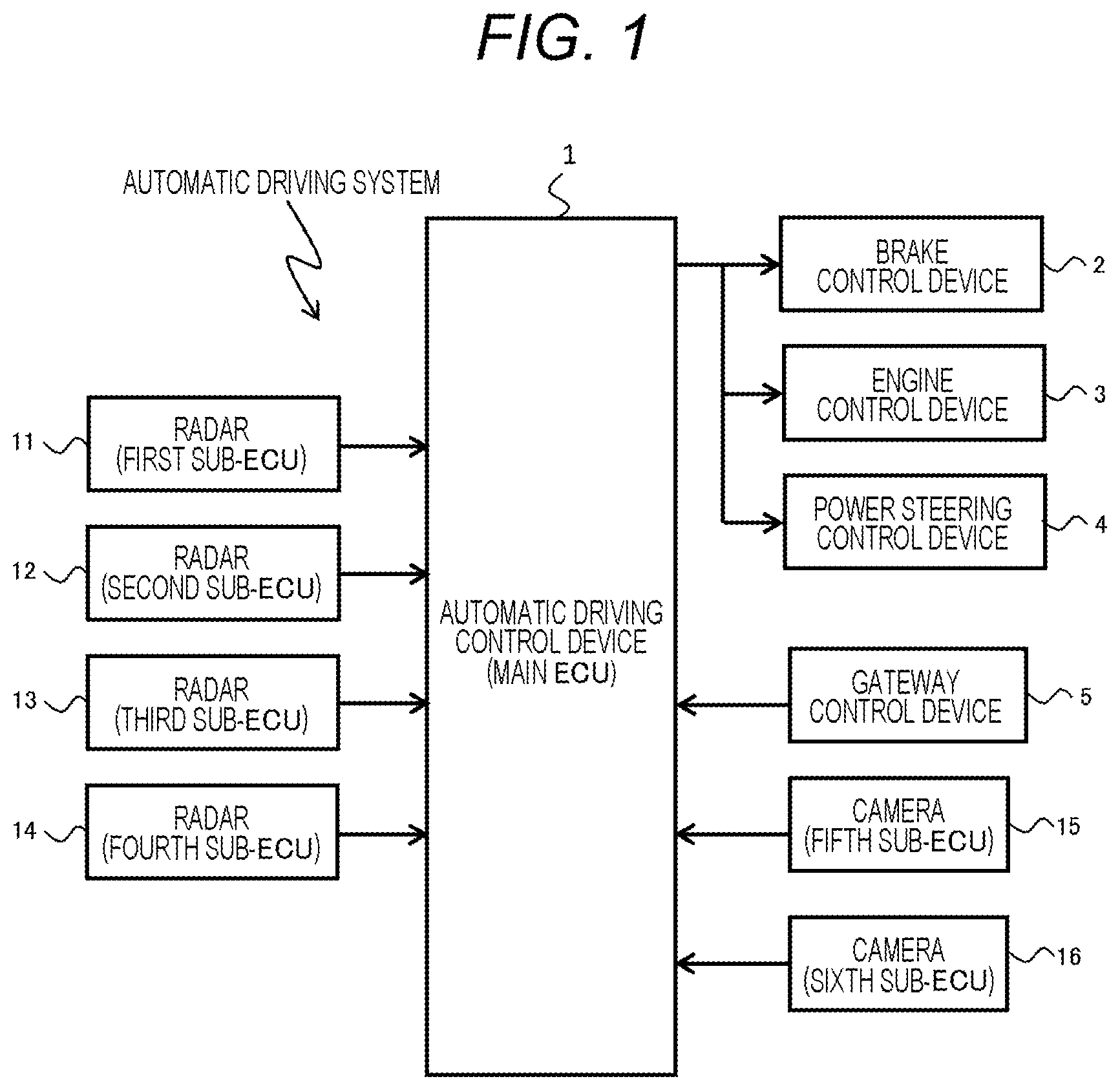
is a schematic configuration example of an automatic driving system in the present embodiment. In , the automatic driving system includes radars 11 , 12 , 13 , and 14 (first main ECU 11 , second sub-ECU 12 , third sub-ECU 13 , fourth sub-ECU 14 ) which are external recognition sensors for recognizing the external situation of the vehicle, and cameras 15 and 16 (fifth sub-ECU 15 , sixth sub-ECU 16 ).
The automatic driving system further includes an automatic driving control device 1 (hereinafter, it is referred to as a main ECU 1 ), a brake control device 2 , an engine control device 3 , a power steering control device 4 , and a gateway control device 5 . Further, the brake control device 2 , the engine control device 3 , and the power steering control device 4 can be collectively called an actuator control device that controls the operation of the vehicle. Each component such as the main ECU 1 and the sub-ECU in constitutes an electronic module.
The first sub-ECU 11 , the second sub-ECU 12 , the third sub-ECU 13 , the fourth sub-ECU 14 , which are radars, and the main ECU 1 , the brake control device 2 , the engine control device 3 , the power steering control device 4 , and the gateway control device 5 are connected by an in-vehicle network (for example, a controller area network (CAN), Ethernet (registered trademark), or the like) so as to be able to communicate with each other.
The brake control device 2 is a control device that performs vehicle brake control (braking force control), and the engine control device 3 is a control device that controls an engine that generates a driving force of the vehicle. In addition, the power steering control device 4 is a control device that controls power steering of the vehicle. The gateway control device 5 is a control device that relays communication with other domains other than the automatic driving system.
Here, when receiving the request for automatic driving, the main ECU 1 calculates a trajectory on which the vehicle moves based on external information from the first sub-ECU 11 to the sixth sub-ECU 16 . Then, the main ECU 1 outputs control commands such as a brake and a driving force to the brake control device 2 , the engine control device 3 , and the power steering control device 4 so as to move the vehicle according to the calculated trajectory. The brake control device 2 , the engine control device 3 , and the power steering control device 4 output an operation signal to each control target (actuator) in response to a control command for automatic driving control from the main ECU 1 .
is a schematic configuration diagram in which the main ECU 1 and the radar 11 (hereinafter, referred to as a first sub-ECU 11 ) in the present embodiment are connected.
In , the main ECU 1 includes a power supply IC 1 a , a microcomputer 1 b , and a communication IC 1 c . The power supply IC 1 a supplies a predetermined voltage to the microcomputer 1 b , and includes an enable signal line 1 d and a transmission/reception communication line 1 e between the microcomputer 1 b and the communication IC 1 c.
The first sub-ECU 11 includes a power supply IC 11 a , a microcomputer lib, and a communication IC 11 c . The power supply IC 11 a supplies a predetermined voltage to the microcomputer 11 b . The microcomputer 11 b communicates with the microcomputer 1 b of the main ECU 1 via the communication ICs 1 c and 11 c , and transmits external information acquired by the sensor to the microcomputer 1 b . Note that the sensor main body is omitted. Communication between main ECU 1 and first sub-ECU 11 is configured as, for example, a CAN bus.
In addition, the first sub-ECU 11 includes a power supply control circuit 11 d that supplies power from a battery power supply VBAT to the power supply IC 11 a , and includes a first switch circuit 11 e and a second switch circuit 11 f in order to control the power supply control circuit lid.
A first switch control line 11 g draws a communication line from a CAN_H signal line or a CAN_L signal line of the CAN bus, connects to the first switch circuit Ile, and controls the first switch circuit lie by voltage fluctuation of the communication line. The first switch control line 11 g is connected from the communication line to the first switch circuit 11 e via the high resistance, so that the influence on the communication line can be reduced.
A second switch control line 11 h is connected to the microcomputer 11 b and controlled by the microcomputer 11 b to hold the power supply control circuit 11 d in the power supply state even when the first switch circuit 11 e is switched on/off by the communication state.
When the first switch control line 11 g is connected to the plus side (CAN_H signal) of the communication line, the second switch circuit 11 f and the second switch control line 11 h may not be provided.
An enable signal line 11 i and a transmission/reception communication line 114 are provided between the microcomputer 11 b and the communication IC 11 c.
is a diagram illustrating a power on/power off sequence of the first sub-ECU 11 according to the present embodiment.
In , by controlling the enable signal line 1 d from the microcomputer 1 b of the main ECU 1 , the voltage of the CAN_H/L signal which is a communication line increases to a recessive voltage (voltage in a standby state).
The voltage of the first switch control line 11 g of the first sub-ECU 11 increases as the voltage of the communication line increases, and when the voltage exceeds a certain threshold voltage, the first switch circuit 11 e works to bring the power supply control circuit 11 d into the power supply state. When power is supplied, the power supply IC 11 a operates, the power supply IC 1 a supplies a predetermined voltage to the microcomputer 11 b , and the microcomputer lib is activated.
When the microcomputer lib is activated, the second switch control line 11 h is controlled to stabilize the power supply of the power supply control circuit lid. Finally, the microcomputer lib controls the enable signal line 11 i so as to be able to communicate with the main ECU 1 .
In a power off sequence, the microcomputer 1 b of the main ECU 1 transmits an end notification to the microcomputer 11 b of the first sub-ECU 11 through a communication line, controls the enable signal line 1 d , and disables the communication IC 1 c.
Upon receiving the end notification, the microcomputer 11 b of the first sub-ECU 11 controls the enable signal line 11 i and disables the communication IC 11 c . Since the communication IC 1 c of the main ECU 1 and the communication IC 11 c of the first sub-ECU are disabled, the voltage of the communication line decreases and the first switch circuit is disabled.
After the end processing of the microcomputer 11 b of the first sub-ECU 11 is performed and the end processing is completed, the second switch control line is controlled to disable the second switch circuit 11 f , so that the power supply control circuit 11 d enters the power off state.
As described above, according to the present embodiment, the main ECU and the sub-ECU are connected by a communication line such as CAN, and when the main ECU becomes communicable, the communication line enters a standby state and the voltage increases. The sub-ECU draws the communication line as a signal line for controlling the power supply control circuit, and controls the power supply control circuit with the increased voltage to supply power to the sub-ECU. That is, the switch circuit is turned on by the voltage (recessive voltage) in the standby state of the communication line to activate the sub-ECU. Since the power supply IC of the sub-ECU does not need to monitor the communication state on the communication line, there is no need to supply power to the power supply IC when the sub-ECU is turned off, and the sub-ECU can provide a wake-up function capable of reducing the dark current.
Therefore, even in an ECU in an advanced driving assistance system such as automatic driving in which dark current is likely to be generated due to connection of a plurality of sensors, it is possible to dedicate and contribute to prevention of battery exhaustion.
Second Embodiment
is a schematic configuration diagram in which a first sub-ECU 11 and a radar 12 (hereinafter, referred to as a second sub-ECU 12 ) are connected to the main ECU 1 according to the present embodiment.
In , similarly to the first sub-ECU 11 , the second sub-ECU 12 includes a power supply IC 12 a , a microcomputer 12 b , and a communication IC 12 c , includes a power supply control circuit 12 d that supplies power from the battery power supply VBAT to the power supply IC 12 a , and includes a first switch circuit 12 e and a second switch circuit 12 f in order to control the power supply control circuit 12 d . Note that the sensor main body is omitted.
The microcomputer 12 b is connected to the same CAN bus as the first sub-ECU 11 in order to communicate with the microcomputer 1 b of the main ECU 1 .
A first switch control line 12 g draws a communication line from the CAN_H signal line or the CAN_L signal line of the CAN bus, connects the communication line to the first switch circuit 12 e , and performs control by voltage fluctuation of the communication line.
A second switch control line 12 h is connected to the microcomputer 12 b and controlled by the microcomputer 12 b to hold the power supply control circuit 12 d in the power supply state even when the first switch circuit 12 e is switched on/off by the communication state.
An enable signal line 12 i and a transmission/reception communication line 12 j are provided between the microcomputer 12 b and the communication IC 12 c.
When the first switch control line 12 g is connected to the plus side (CAN_H signal) of the communication line, the second switch circuit 12 f and the second switch control line 12 h may not be provided.
The power on/off sequence of the first sub-ECU 11 and the second sub-ECU 12 in the present embodiment is similar to the sequence of the first embodiment illustrated in , and thus the description thereof will be omitted. In the present embodiment, the case where two sub-ECUs are connected to the main ECU has been described, but the same configuration and effect can be obtained even if three or more sub-ECUs are connected.
As described above, according to the present embodiment, even in the case of the main ECU and the plurality of sub-ECUs, the sub-ECU can provide the wake-up function capable of reducing the dark current as in the first embodiment, and can dedicate and contribute to the prevention of battery exhaustion even in the ECU in the advanced driving assistance system such as the automatic driving in which the dark current is likely to be generated by the connection of the plurality of sensors.
Third Embodiment
is a schematic configuration diagram of the main ECU 1 according to the present embodiment.
In , the main ECU 1 includes a main board 100 and sub-boards 101 and 102 . The sub-boards 101 and 102 realize functions of additional options necessary in a scene of automatic driving. Communication between the main board 100 and the sub-board 101 and communication between the main board 100 and the sub-board 102 are configured by, for example, a universal asynchronous receiver/transmitter (UART) or a serial peripheral interface (SPI). The main board 100 and the sub-boards 101 and 102 constitute an electronic module.
In , the main board 100 includes a power supply IC 100 a and a first microcomputer 100 b , communication with the sub-board 101 is performed by a UART communication line 100 c , and communication with the sub-board 102 is performed by an SPI communication line 100 e . The sub-board is connected by connectors 100 g and 100 h.
The sub-board 101 includes a power supply IC 101 a and a second microcomputer 101 b , includes a power supply control circuit 101 c that supplies power from the battery power supply VBAT to the power supply IC 101 a , and includes a first switch circuit 101 d and a second switch circuit 101 e in order to control the power supply control circuit 101 c . The main board is connected by a connector 101 h.
A first switch control line 101 f draws a communication line inside from the TX signal line of the UART, connects to the first switch circuit 101 d , and performs control by voltage fluctuation of the communication line.
A second switch control line 101 g is connected to the second microcomputer 101 b and controlled by the second microcomputer 101 b to hold the power supply control circuit 101 c in the power supply state even when the first switch circuit 101 d is switched on/off due to the communication state.
Similarly to the sub-board 101 , the sub-board 102 includes a power supply IC 102 a and a third microcomputer 102 b , includes a power supply control circuit 102 c that supplies power from a battery power supply VBAT to the power supply IC 102 a , and includes a first switch circuit 102 d and a second switch circuit 102 e in order to control the power supply control circuit 102 c . The main board is connected by a connector 102 h.
A first switch control line 102 f draws a communication line from a CS signal line of the SPI, connects the communication line to the first switch circuit 102 d , and performs control by voltage fluctuation of the communication line.
A second switch control line 102 g is connected to the third microcomputer 102 b and controlled by the third microcomputer 102 b to hold the power supply control circuit 102 c in the power supply state even when the first switch circuit 102 d is switched on/off due to the communication state.
is a diagram illustrating a power on/power off sequence of the sub-board 101 according to the present embodiment.
In , by bringing the UART communication line 100 c of the first microcomputer 100 b of the main board 100 into the communicable state, the voltage of a TX signal line 100 d increases to the high level. The voltage of the first switch control line 101 f of the sub-board 101 increases as the voltage of the communication line increases, and when the voltage exceeds a certain threshold voltage, the first switch circuit 101 d works to bring the power supply control circuit 101 c into the power supply state. When power is supplied, the power supply IC 101 a operates to activate the second microcomputer 101 b.
When the second microcomputer 101 b is activated, the second switch control line 101 g is controlled to stabilize the power supply of the power supply control circuit 101 c.
In the power off sequence, the first microcomputer 100 b of the main board 100 transmits an end notification to the second microcomputer 101 b of the sub-board 101 via a communication line, and the voltage is dropped to the low level of the TX signal line 100 d of the UART communication line 100 c , thereby disabling the UART communication.
When the TX signal line 100 d falls to the Low level, the voltage of the first switch control line 101 f decreases, and the first switch circuit 101 d becomes disabled.
Upon receiving the end notification, the second microcomputer 10 b performs the end processing of the second microcomputer 101 b , and after the end processing is completed, the second switch control line 101 g is controlled to disable the second switch circuit 101 e , so that the power supply control circuit 101 c enters the power off state.
By monitoring the voltage of the RX signal line of the UART communication line 100 c , the first microcomputer 100 b of the main board 100 can confirm that the power supply to the sub-board 101 is cut off.
is a diagram illustrating a power on/power off sequence of the sub-board 102 according to the present embodiment.
In , by bringing the SPI communication line 100 e of the first microcomputer 100 b of the main board 100 into the communicable state, the voltage of the CS signal line 100 f rises to the High level. The voltage of the first switch control line 102 f of the sub-board 102 increases as the voltage of the communication line increases, and when the voltage exceeds a certain threshold voltage, the first switch circuit 102 d works to bring the power supply control circuit 102 c into the power supply state. When power is supplied, the power supply IC 102 a operates to activate the third microcomputer 102 b.
When the third microcomputer 102 b is activated, the second switch control line 102 g is controlled to stabilize the power supply of the power supply control circuit 102 c . The third microcomputer 102 b controls the enable signal line so as to be communicable with the first microcomputer 100 b of the main board 100 .
In the power off sequence, the first microcomputer 100 b of the main board 100 transmits an end notification to the third microcomputer 102 b of the sub-board 102 through a communication line, and the voltage of a CS signal line 100 f of the SPI communication line 100 e is dropped to the Low level to disable the SPI communication.
When the CS signal line 100 f falls to the Low level, the voltage of the first switch control line 102 f decreases, and the first switch circuit 102 d becomes disabled.
Upon receiving the end notification, the third microcomputer 102 b performs the end processing of the third microcomputer 102 b , and after the end processing is completed, controls the second switch control line 102 g to disable the second switch circuit 102 e , so that the power supply control circuit 102 c enters the power off state.
The first microcomputer 100 b of the main board 100 monitors a DIN signal line by setting the IDLE state of the DIN signal line of the SPI communication line 100 e to High (pull-up setting) or the like, so that it can be confirmed that the power supply to the sub-board 102 is cut off.
As described above, according to the present embodiment, since the switch circuit is turned on by the voltage in the standby state of the communication line to activate the sub-board, there is no need to supply power to the power supply IC when the sub-board is turned off, and the sub-board can provide power supply control capable of reducing dark current.
Although the embodiments have been described above, the present invention is not limited to the above-described embodiments and includes various modifications. For example, the present invention is not limited to a vehicle or an automobile, and is applicable to any electronic module connected via a communication line. The above embodiments have been described in detail for easy understanding of the present invention, and the present invention is not necessarily limited to those having all the configurations described. Some of the configurations of a certain embodiment may be replaced with the configurations of the other embodiments, and the configurations of the other embodiments may be added to the configurations of the subject embodiment. It is possible to add, delete, and replace other configurations for a part of the configuration of each embodiment.
REFERENCE SIGNS LIST
•
• 1 automatic driving control device (main ECU) • 2 brake control device • 3 engine control device • 4 power steering control device • 5 gateway control device • 11 , 12 , 13 , 14 radar (first to fourth sub-ECUs) • 15 , 16 camera (fifth and sixth sub-ECUs) • 1 a , 11 a , 12 a power supply IC • 1 b , 11 b , 12 b microcomputer • 1 c , 11 c , 12 c communication IC • 11 d , 12 d , 101 c , 102 c power supply control circuit • 11 e , 12 e , 101 d , 102 d first switch circuit • 11 f , 12 f , 101 e , 102 e second switch circuit • 11 g , 12 g , 101 f , 102 f first switch control line • 11 h , 12 h , 101 g , 102 g second switch control line • 1 d , 11 i , 12 i enable signal line • 1 e , 11 j , 12 j transmission/reception communication line • 100 main board • 101 , 102 sub-board • 100 a , 101 a , 102 a power supply IC • 100 b first microcomputer • 100 c UART communication line • 100 d TX signal line • 100 e SPI communication line • 100 f CS signal line • 100 g , 100 h , 101 h , 102 h connector • 101 b second microcomputer • 102 b third microcomputer
Figures (5)
Citations
This patent cites (13)
- US2004/0083234
- US2004/0186938
- US2010/0299466
- US2012/0054526
- US2018/0057008
- US2019/0050522
- US2022/0317753
- US2009-202822
- US2011-235770
- US2012-51422
- US2016-172503
- US2020-65333
- USWO 2019/239876