Abstract
A semiconductor package includes first semiconductor chips stacked on a package substrate, a lowermost first semiconductor chip of the first semiconductor chips including a recessed region, and a second semiconductor chip inserted in the recessed region, the second semiconductor chip being connected to the package substrate.
Claims (20)
1 . A semiconductor package, comprising: a first set of semiconductor chips stacked on a package substrate and including a lowermost semiconductor chip and a plurality of semiconductor chips stacked on the lowermost semiconductor chip, the lowermost semiconductor chip of the first set of semiconductor chips including a first protruding portion protruding horizontally in a horizontal direction parallel to a top surface of the package substrate to overhang above the package substrate; a second set of semiconductor chips stacked on the package substrate and including a lowermost semiconductor chip and a plurality of semiconductor chips stacked on the lowermost semiconductor chip, the lowermost semiconductor chip of the second set of semiconductor chips including a second protruding portion protruding horizontally in a direction parallel to the top surface of the package substrate to overhang the package substrate, such that the first protruding portion faces the second protruding portion with a gap therebetween; and an additional semiconductor chip disposed below the first protruding portion and the second protruding portion to overlap each of the first protruding portion and the second protruding portion in a vertical direction perpendicular to the horizontal direction, the additional semiconductor chip being electrically connected to the package substrate, wherein the additional semiconductor chip is disposed between the first protruding portion and the package substrate and between the second protruding portion and the package substrate.
13 . A semiconductor package, comprising: a package substrate; a first semiconductor chip on a center region of the package substrate, the first semiconductor chip being electrically connected to the package substrate, and the first semiconductor chip having a first side surface and a second side surface, which are opposite to each other in a horizontal direction; and second to fifth semiconductor chips, each overlapping the first side surface of the first semiconductor chip, the second to fifth semiconductor chips being sequentially stacked on the first semiconductor chip in the vertical direction, and the second to fifth semiconductor chips being electrically connected to the package substrate, wherein the second semiconductor chip includes a first semiconductor substrate and a first circuit layer on the first semiconductor substrate, wherein the first semiconductor substrate includes a first recessed region, in which the first semiconductor chip is inserted, so that part of the first semiconductor chip is between the second semiconductor chip and the package substrate to be covered by the second semiconductor chip, and part of the first semiconductor chip is not covered by the second semiconductor chip, and the first recessed region has a depth in a range from 90 μm to 780 μm, when measured from a lowermost surface of the first semiconductor substrate.
17 . A semiconductor package, comprising: a package substrate; a first semiconductor chip on and electrically connected to the package substrate; a second semiconductor chip on the first semiconductor chip, the second semiconductor chip having a recessed region, in which the first semiconductor chip is inserted, so that the first semiconductor chip is between the package substrate and a protruding portion of the second semiconductor chip formed above the recessed region; a first wire connecting the second semiconductor chip to the package substrate; a third semiconductor chip on the second semiconductor chip; a second wire connecting the third semiconductor chip to the second semiconductor chip; and a first adhesive layer between the second semiconductor chip and the third semiconductor chip, an upper portion of the second wire being buried in the first adhesive layer.
Show 17 dependent claims
2 . The semiconductor package as claimed in claim 1 , wherein the semiconductor chips of the first set of semiconductor chips have a same function and have a same top surface size as each other when viewed from a plan view.
3 . The semiconductor package as claimed in claim 1 , wherein each of the lowermost first semiconductor chip of the first set of semiconductor chips and the lowermost semiconductor chip of the second set of semiconductor chips includes: a semiconductor substrate; and a circuit layer on the semiconductor substrate, wherein a recessed region below the protruding portion is disposed in the semiconductor substrate, and wherein the additional semiconductor chip is disposed between the package substrate and the circuit layer of each lowermost semiconductor chip.
4 . The semiconductor package as claimed in claim 3 , wherein for each lowermost semiconductor chip, a recessed region is formed beneath the protruding portion, and a surface roughness of a surface of the recessed region is different from a surface roughness of a side surface of the semiconductor substrate.
5 . The semiconductor package as claimed in claim 4 , wherein the recessed region has a depth in a range from 90 μm to 780 μm, when measured from a lowermost surface of the semiconductor substrate.
6 . The semiconductor package as claimed in claim 1 , further comprising a mold layer covering the first set of semiconductor chips and the second set of semiconductor chips, the mold layer extending under the first protruding portion and under the second protruding portion, to cover the additional semiconductor chip.
7 . The semiconductor package as claimed in claim 1 , further comprising: a first adhesive layer between the lowermost semiconductor chip of the first set of semiconductor chips and the package substrate, the first adhesive layer having a first thickness; and second adhesive layers between adjacent ones of the semiconductor chips of the first set of semiconductor chips other than the lowermost semiconductor chip of the first set of semiconductor chips, at least one of the second adhesive layers having a second thickness different from the first thickness.
8 . The semiconductor package as claimed in claim 7 , further comprising a wire connecting one of the semiconductor chips of the first set of semiconductor chips to another of the semiconductor chips of the first set of semiconductor chips, the wire being buried in one of the second adhesive layers.
9 . The semiconductor package as claimed in claim 1 , wherein the first set of semiconductor chips is arranged in a mirror symmetric structure with respect to the second set of semiconductor chips, and two opposite end portions of the additional semiconductor chip overlap the two stacks, respectively.
10 . The semiconductor package as claimed in claim 1 , wherein a portion of the additional semiconductor chip is not covered by any of the semiconductor chips of the first set of semiconductor chips and is not covered by any of the semiconductor chips of the second set of semiconductor chips.
11 . The semiconductor package as claimed in claim 1 , wherein the first protruding portion overhangs a first wire formed therebelow and connecting the package substrate to the additional semiconductor chip, and the second protruding portion overhangs a second wire formed therebelow and connecting the package substrate to the additional semiconductor chip.
12 . The semiconductor package as claimed in claim 1 , wherein: the protruding portion of the lowermost chip of the first set of semiconductor chips includes a bottom surface overlapping and facing a first portion of a top surface of the additional semiconductor chip, and said bottom surface and top surface are electrically isolated from each other; and the protruding portion of the lowermost chip of the second set of semiconductor chips includes a bottom surface overlapping and facing a second portion of a top surface of the additional semiconductor chip, and said bottom surface and top surface are electrically isolated from each other.
14 . The semiconductor package as claimed in claim 13 , wherein the second to fifth semiconductor chips overlap a third side surface of the first semiconductor chip.
15 . The semiconductor package as claimed in claim 13 , further comprising sixth to ninth semiconductor chips, each overlapping the second side surface of the first semiconductor chip, the sixth to ninth semiconductor chips sequentially stacked on the first semiconductor chip, and are electrically connected to the package substrate, wherein the sixth semiconductor chip includes a second semiconductor substrate and a second circuit layer on the second semiconductor substrate, wherein the second semiconductor substrate includes a second recessed region, in which the first semiconductor chip is inserted, and wherein the second recessed region has a depth in a range from 90 μm to 780 μm, when measured from a lowermost surface of the second semiconductor substrate.
16 . The semiconductor package as claimed in claim 15 , wherein the sixth to ninth semiconductor chips and the second to fifth semiconductor chips are arranged in a mirror symmetric shape.
18 . The semiconductor package as claimed in claim 17 , wherein the second semiconductor chip includes a semiconductor substrate and a circuit layer on the semiconductor substrate, the recessed region being in the semiconductor substrate.
19 . The semiconductor package as claimed in claim 18 , wherein a surface roughness of a surface of the recessed region is different from a surface roughness of a side surface of the semiconductor substrate.
20 . The semiconductor package as claimed in claim 17 , further comprising a second adhesive layer between the first semiconductor chip and the package substrate, the second adhesive layer having a second thickness smaller than a first thickness of the first adhesive layer.
Full Description
Show full text →
CROSS-REFERENCE TO RELATED APPLICATION
This U.S. non-provisional patent application claims priority under 35 U.S.C. § 119 to Korean Patent Application No. 10-2021-0088913, filed on Jul. 7, 2021, in the Korean Intellectual Property Office, the entire contents of which are hereby incorporated by reference.
BACKGROUND
1. Field The present disclosure relates to a semiconductor package. 2. Description of the Related Art A semiconductor package is configured to easily use an integrated circuit chip as a part of an electronic product. Conventionally, the semiconductor package includes a printed circuit board (PCB) and a semiconductor chip die, which is mounted on the PCB and is electrically connected to the PCB using bonding wires or bumps. With development of the electronic industry, many studies are being conducted to improve reliability and durability of the semiconductor package.
SUMMARY
According to an embodiment, a semiconductor package may include first semiconductor chips stacked on a package substrate, wherein a lowermost first semiconductor chip of the first semiconductor chips includes a recessed region, and a second semiconductor chip is inserted in the recessed region and connected to the package substrate. According to an embodiment, a semiconductor package may include a first semiconductor chip disposed on a center region of a package substrate and connected to the package substrate, the first semiconductor chip having a first side surface and a second side surface, which are opposite to each other, and second to fifth semiconductor chips overlapping the first side surface of the first semiconductor chip, sequentially stacked on the first semiconductor chip, and connected to the package substrate. The second semiconductor chip may include a first semiconductor substrate and a first circuit layer on the first semiconductor substrate. The first semiconductor substrate may be provided to define a first recessed region, in which the first semiconductor chip is inserted. The first recessed region may have a depth ranging from 90 μm to 780 μm, when measured from the lowermost portion of a bottom surface of the first semiconductor substrate. According to an embodiment, a semiconductor package may include a first semiconductor chip disposed on and connected to a package substrate, a second semiconductor chip disposed on the first semiconductor chip, the second semiconductor chip having a recessed region, in which the first semiconductor chip is inserted, a wire connecting the second semiconductor chip to the package substrate, a third semiconductor chip on the second semiconductor chip, and a first adhesive layer between the second semiconductor chip and the third semiconductor chip. An upper portion of the wire may be buried in the first adhesive layer.
BRIEF DESCRIPTION OF THE DRAWINGS
Features will become apparent to those of skill in the art by describing in detail exemplary embodiments with reference to the attached drawings, in which: is a plan view of a semiconductor package according to an embodiment. is a cross-sectional view taken along a line A-A′ of . is an enlarged cross-sectional view of portion ‘P 1 ’ of . A is a plan view of a second semiconductor chip according to an embodiment. B is a perspective view of the second semiconductor chip having the planar structure of A . is an enlarged cross-sectional view of portion ‘P 2 ’ of . is a cross-sectional view of a second semiconductor chip according to an embodiment. A and 8 A are plan views of stages in a process of fabricating the second semiconductor chip of . B and 8 B are cross-sectional views along line C-C′ of A and 8 A . A to 9 D are cross-sectional views of stages in a process of fabricating the semiconductor package of . is a plan view of a semiconductor package according to an embodiment. is a cross-sectional view taken along line D-D′ of . is a cross-sectional view taken along line E-E′ of . is a perspective view of a second semiconductor chip in the semiconductor package of . A is a plan view of a process of fabricating the second semiconductor chip of . B is a cross-sectional view taken along line C-C′ of A . is a cross-sectional view of a semiconductor package according to an embodiment. is a perspective view of a second semiconductor chip in the semiconductor package of . A is a plan view of a second semiconductor chip according to an embodiment. B is a perspective view of the second semiconductor chip of A . is a plan view of a semiconductor package according to an embodiment.
DETAILED DESCRIPTION
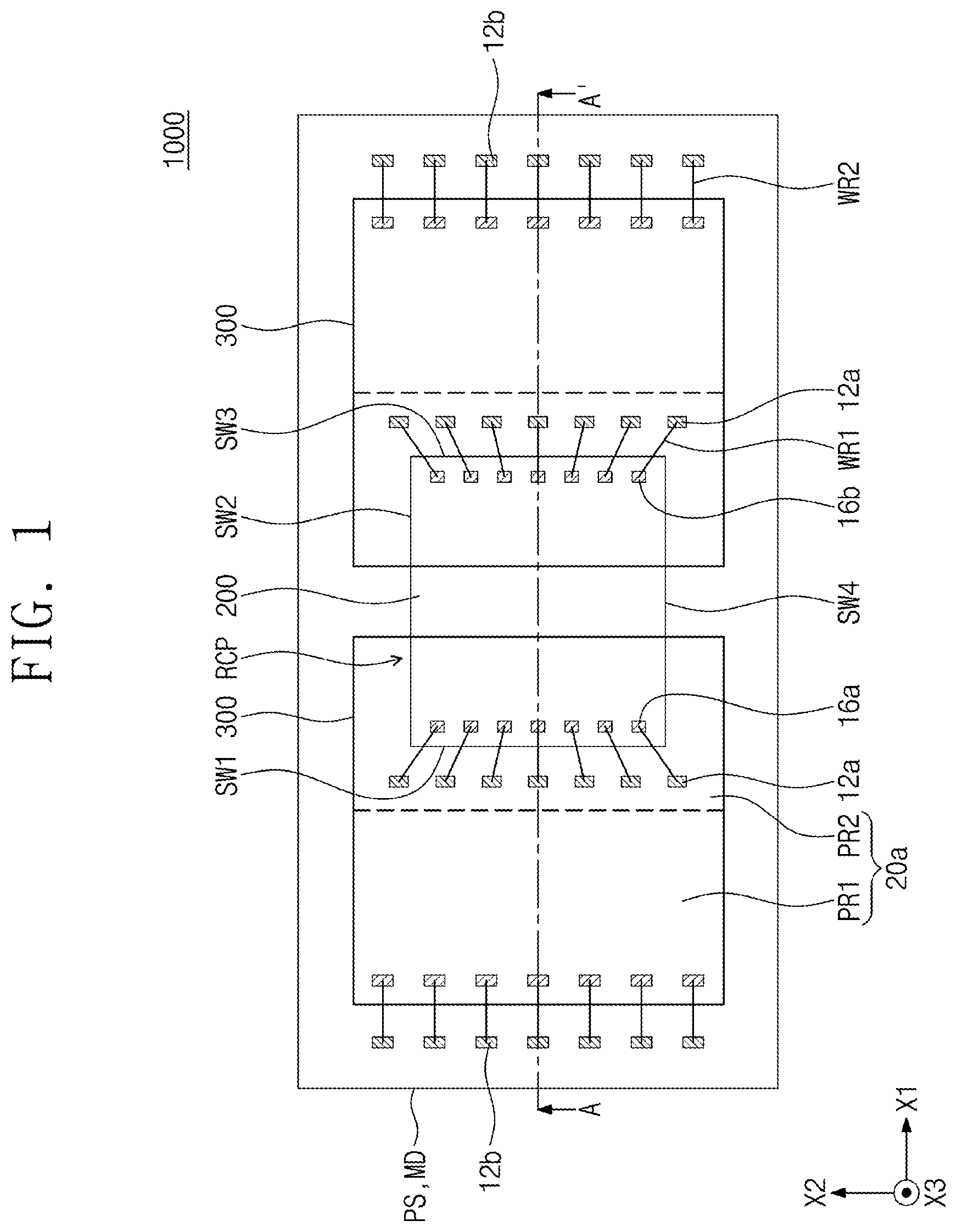
Example embodiments will now be described more fully with reference to the accompanying drawings, in which example embodiments are shown. Like reference numerals in the drawings denote like elements, and thus their description will be omitted. is a plan view illustrating a semiconductor package according to an embodiment. is a cross-sectional view along line A-A′ of , and is an enlarged sectional view of portion ‘P 1 ’ of . Referring to to 3 , in a semiconductor package 1000 according to the present embodiment, a first semiconductor chip 200 may be mounted on a center region of a package substrate PS. Second to fifth semiconductor chips 300 , 310 , 320 , and 330 may be sequentially stacked on regions of the package substrate PS which are located at both sides of the first semiconductor chip 200 . The second to fifth semiconductor chips 300 , 310 , 320 , and 330 , the first semiconductor chip 200 , and the package substrate PS may be covered with a mold layer MD. The package substrate PS may be, e.g., a double-sided or multi-layered printed circuit board. In an embodiment, the package substrate PS may be a redistribution substrate. The package substrate PS may include an insulating portion 40 , first and second upper conductive pads 12 a and 12 b disposed on a top surface of the insulating portion 40 , and ball lands 10 disposed on a bottom surface of the insulating portion 40 . Outer connection terminals OSB may be bonded to the ball lands 10 . The outer connection terminals OSB may include at least one of, e.g., conductive bumps, conductive pillars, or solder balls. The outer connection terminals OSB may be formed of or include at least one of, e.g., tin, lead, silver, copper, aluminum, gold, or nickel. The package substrate PS may further include internal lines 14 disposed in the insulating portion 40 . The internal lines 14 may be provided to connect some of the first and second upper conductive pads 12 a and 12 b to each other or to connect others of the first and second upper conductive pads 12 a and 12 b to the ball lands 10 . The first and second upper conductive pads 12 a and 12 b , the ball lands 10 , and the internal lines 14 may be formed of or include at least one of metallic materials (e.g., titanium, copper, aluminum, nickel, and gold). The insulating portion 40 may include a plurality of insulating layers which are stacked. The insulating layers may be formed of or include at least one of thermosetting resins (e.g., epoxy resin), thermoplastic resins (e.g., polyimide), composite materials (e.g., prepreg or fire resist-4 (FR4)), in which a reinforcement element (e.g., glass fiber and/or inorganic filler) is pre-impregnated with a thermoplastic or thermosetting resin matrix, photo-curable resin and/or photo-imagable dielectric (PID). In an embodiment, the first semiconductor chip 200 may be configured to have a different function from the second to fifth semiconductor chips 300 , 310 , 320 , and 330 . For example, all of the second to fifth semiconductor chips 300 , 310 , 320 , and 330 may be memory chips of the same kind, and the first semiconductor chip 200 may be a logic or control chip, which is used to control the second to fifth semiconductor chips 300 , 310 , 320 , and 330 . Alternatively, the first semiconductor chip 200 may be one of, e.g., a microelectromechanical system (MEMS) chip, an application-specific integrated circuit (ASIC) chip, or a central processing unit (CPU) chip. The memory chip may be, e.g., a NAND chip, a VNAND chip, a dynamic random-access memory (DRAM) chip, a static random-access memory (SRAM) chip, an electrically erasable programmable read-only memory (EEPROM) chip, a phase change random-access memory (PRAM) chip, a magnetoresistive random-access memory (MRAM) chip, a resistive random-access memory (ReRAM) chip, a high bandwidth memory (HBM) chip, or a hybrid memory cubic (HMC) chip. In an embodiment, the second to fifth semiconductor chips 300 , 310 , 320 , and 330 may be of different kinds. The first semiconductor chip 200 may include first chip first upper pads 16 a and first chip second upper pads 16 b , which are disposed on a top surface of the first semiconductor chip 200 . The first chip first upper pads 16 a and the first chip second upper pads 16 b may be electrically connected to the first upper conductive pads 12 a by first wires WR 1 , respectively. The first semiconductor chip 200 may have first to fourth chip side surfaces SW 1 to SW 4 in a clockwise direction ( ). The first semiconductor chip 200 may have a first thickness T 1 ( ). Upper portions of the first wires WR 1 , which are located above the first semiconductor chip 200 , may have a first height H 1 from a top surface 200 _U of the first semiconductor chip 200 ( ). For example, as illustrated in , the first semiconductor chip 200 may be mounted on the package substrate PS in a wire bonding manner. In another example, the first semiconductor chip 200 may be mounted in a flip-chip bonding manner. In an embodiment, the second to fifth semiconductor chips 300 , 310 , 320 , and 330 may be configured to have the same features as each other. For example, the second to fifth semiconductor chips 300 , 310 , 320 , and 330 may have the same function, the same electrical circuit structure, and the same size. For example, each of the second to fifth semiconductor chips 300 , 310 , 320 , and 330 may have the first width W 1 of in a first direction X 1 and may have a second width W 2 of B in a second direction X 2 . Each of the second to fifth semiconductor chips 300 , 310 , 320 , and 330 may have the second thickness T 2 of . Each of the second to fifth semiconductor chips 300 , 310 , 320 , and 330 may include a semiconductor substrate 20 or 20 a and a circuit layer 24 . The semiconductor substrate 20 or 20 a may include a top surface 20 U and a bottom surface 20 B, which are opposite to each other. The circuit layer 24 may be disposed on the top surface 20 U of the semiconductor substrate 20 . The circuit layer 24 may include transistors TR, an interlayer insulating layer ILD covering the transistors TR, and interconnection patterns 22 disposed in the interlayer insulating layer ILD. The interlayer insulating layer ILD may be formed of or include at least one of, e.g., silicon oxide, silicon nitride, silicon oxynitride, porous insulating materials and may have a single- or multi-layered structure. Second chip upper pads 26 may be disposed in an uppermost portion of the interlayer insulating layer ILD and may be connected to the interconnection patterns 22 . A is a plan view illustrating the second semiconductor chip 300 of . B is a perspective view illustrating the second semiconductor chip 300 . It is noted that the second semiconductor chip 300 of corresponds to a cross-section along line B-B′ of A , and B illustrates an inverted structure of the second semiconductor chip 300 of . Referring to to 4 B , the lowermost one of the second to fifth semiconductor chips 300 , 310 , 320 , and 330 (i.e., the second semiconductor chip 300 ) may have a recessed region RCP, in which the first semiconductor chip 200 is inserted. The recessed region RCP may be defined by the bottom surface 20 B of the semiconductor substrate 20 a of the second semiconductor chip 300 . In an embodiment, the semiconductor substrate 20 a of the second semiconductor chip 300 may include a first substrate portion PR 1 and a second substrate portion PR 2 . The first substrate portion PR 1 may have a third thickness T 3 . The second substrate portion PR 2 may have a fourth thickness T 4 that is smaller than the third thickness T 3 . The first substrate portion PR 1 may protrude relative to the second substrate portion PR 2 , e.g., along the first direction X 1 , and may be referred to as a ‘protruding portion’. A bottom surface of the second substrate portion PR 2 may be located at a level different from a bottom surface of the first substrate portion PR 1 , e.g., relative to the package substrate PS along the third direction X 3 . The recessed region RCP may be referred to as a ‘stepped region’. The recessed region RCP may not be formed in each of the third to fifth semiconductor chips 310 , 320 , and 330 , e.g., the recessed region RCP may be formed only in the second semiconductor chip 300 among the second to fifth semiconductor chips 300 to 330 to accommodate the first semiconductor chip 200 therein. When viewed in the plan view of A , the second semiconductor chip 300 may include four corners CR 1 to CR 4 arranged in a counter-clockwise direction. The first substrate portion PR 1 may overlap the first and second corners CR 1 and CR 2 but may be spaced apart from the third and fourth corners CR 3 and CR 4 . When viewed in a plan view, each of the first and second substrate portions PR 1 and PR 2 may have a rectangular shape. In the embodiment of B , when measured in the first direction X 1 , the first substrate portion PR 1 may have a third width W 3 and the second substrate portion PR 2 may have a fourth width W 4 . The third width W 3 may be equal to or different from the fourth width W 4 . A sum of the third and fourth widths W 3 and W 4 may equal the first width W 1 . The fourth width W 4 may be about 10% to about 90% of the first width W 1 . When measured in the second direction X 2 , each of the first and second substrate portions PR 1 and PR 2 may have the second width W 2 . is an enlarged cross-sectional view of portion ‘P 2 ’ of . Portion P 2 illustrated an enlarged view of a corner of the second substrate portion PR 2 . Referring to , a surface RCP_S of the recessed region RCP of the semiconductor substrate 20 a (i.e., a surface of the second substrate portion PR 2 facing the first semiconductor chip 200 ), which is included in the second semiconductor chip 300 , may have a first surface roughness. Further, a side surface 20 SW of the semiconductor substrate 20 a (i.e., a surface of the second substrate portion PR 2 extending from and perpendicular to the surface RCP_S) may have a second surface roughness different from the first surface roughness. In an embodiment, the first surface roughness may be smaller than the second surface roughness. Alternatively, the first surface roughness may be greater than the second surface roughness. Referring back to B , the recessed region RCP may have a first depth DT from the bottom surface 20 B of the first substrate portion PR 1 of the semiconductor substrate 20 a . The first depth DT may be equal to a difference between the third thickness T 3 and the fourth thickness T 4 . The first depth DT may be equal to or larger than a sum of the first thickness T 1 of the first semiconductor chip 200 and the first height H 1 of an upper portion of the first wire WR 1 located above the first semiconductor chip 200 . For example, the third thickness T 3 may range from about 600 μm to about 800 μm, and the fourth thickness T 4 may range from about 20 μm to about 710 μm. For example, the first depth DT may range from about 90 μm to about 780 μm. For example, the first thickness T 1 may be about 60 μm, and the first height H 1 may be about 30 μm. The first semiconductor chip 200 may be attached to the package substrate PS using a first adhesive layer AD 1 of a fifth thickness T 5 . A second adhesive layer AD 2 of a sixth thickness T 6 may be interposed between the first substrate portion PR 1 of the second semiconductor chip 300 and the package substrate PS. A third adhesive layer AD 3 of a seventh thickness T 7 may be interposed between the second semiconductor chip 300 and the third semiconductor chip 310 . A fourth adhesive layer AD 4 of an eighth thickness T 8 may be interposed between the third semiconductor chip 310 and the fourth semiconductor chip 320 . A fifth adhesive layer AD 5 may be interposed between the fourth semiconductor chip 320 and the fifth semiconductor chip 330 . The fifth thickness T 5 may be equal to or smaller than the sixth thickness T 6 . Accordingly, the first semiconductor chip 200 may be stably inserted in the recessed region RCP. In addition, the fifth thickness T 5 may be equal to or smaller than the eighth thickness T 8 . The seventh thickness T 7 may be smaller than the sixth thickness T 6 and/or the eighth thickness T 8 . Accordingly, it may be possible to reduce a total thickness of the semiconductor package 1000 . In an embodiment, all of the first to fifth adhesive layers AD 1 to AD 5 may be formed of or include the same adhesive material. At least one of the first to fifth adhesive layers AD 1 to AD 5 may be a die attach film (DAF). The third and fifth semiconductor chips 310 and 330 may protrude relative to the second and fourth semiconductor chips 300 and 320 in the first direction X 1 . A second wire WR 2 may be provided to connect the second chip upper pad 26 of the third or second semiconductor chip 310 or 300 to the second upper conductive pad 12 b . An upper portion of the second wire WR 2 may protrude from a top surface of the third semiconductor chip 310 by the first height H 1 . The upper portion of the second wire WR 2 may be buried in the fourth adhesive layer AD 4 . The eighth thickness T 8 may be equal to or larger than the first height H 1 . A third wire WR 3 may be provided to connect the second chip upper pad 26 of the fifth or fourth semiconductor chip 330 or 320 to the second upper conductive pad 12 b . An upper portion of the third wire WR 3 may protrude from a top surface of the fifth semiconductor chip 330 by the first height H 1 . As illustrated in , the second to fifth semiconductor chips 300 , 310 , 320 , and 330 of a first set SET 1 , i.e., a first stack, may be disposed on the first chip side surface SW 1 of the first semiconductor chip 200 , and the second to fifth semiconductor chips 300 , 310 , 320 , and 330 of a second set SET 2 , e.g., a second stack, may be disposed on a third chip side surface SW 3 of the first semiconductor chip 200 . The second set SET 2 and the first set SET 1 , e.g., the two stacks, may be spaced apart from each other, e.g., along the first direction X 1 , and may have a mirror symmetric structure, e.g., with respect to the third direction X 3 . The mold layer MD may extend into a region between the second to fifth semiconductor chips 300 , 310 , 320 , and 330 of the first set SET 1 and the second to fifth semiconductor chips 300 , 310 , 320 , and 330 of the second set SET 2 to fill the recessed regions RCP, e.g., around the first semiconductor chip 200 . The mold layer MD may be formed of or include an insulating resin (e.g., epoxy molding compound (EMC)). The mold layer MD may further include fillers, which are distributed in the insulating resin. The filler may be an inorganic filler (e.g., containing at least one of silica, alumina, or titania) or an organic filler (e.g., containing a polymeric material). For example, as illustrated in , the number of the semiconductor chips 300 , 310 , 320 , and 330 , which overlap an end portion of the first semiconductor chip 200 and constitute one set, may be four. In another example, the number of the semiconductor chips overlapping the end portion of the first semiconductor chip 200 may be 1 to 3 or may be equal to or larger than 5. In the semiconductor package 1000 according to the present embodiment, the lowermost one of the second to fifth semiconductor chips 300 , 310 , 320 , and 330 (i.e., the second semiconductor chip 300 ) may be provided to have the recessed region RCP, in which the first semiconductor chip 200 can be inserted. Accordingly, it may be possible to remarkably reduce at least one of horizontal and/or vertical sizes of the semiconductor package 1000 . For example, the semiconductor package 1000 according to the present embodiment may have a reduced bond-level thickness. Accordingly, it may be possible to reduce fabrication cost and turnaround time (TAT). If the second semiconductor chip 300 does not have the recessed region RCP, the first semiconductor chip 200 , which controls the second to fifth semiconductor chips 300 , 310 , 320 , and 330 , may be placed around, e.g., horizontally adjacent to, the second to fifth semiconductor chips 300 , 310 , 320 , and 330 , and in this case, a horizontal size of a semiconductor package may be increased. In certain cases, the first semiconductor chip 200 could be potentially disposed below the second to fifth semiconductor chips 300 , 310 , 320 , and 330 using a spacer or a supporter, but in this case, a vertical size of a semiconductor package may be increased. In contrast, according to an embodiment, by stacking memory chips, e.g., the second to fifth semiconductor chips 300 , 310 , 320 , and 330 , and inserting the first semiconductor chip 200 within a recess of a lowest one of the stacked memory chip, it may be possible to realize a highly-integrated compact semiconductor package with large memory capacity. In addition, according to an embodiment, it may be unnecessary to provide a spacer or a supporter. is a cross-sectional view illustrating a second semiconductor chip according to an embodiment. Referring to , a second semiconductor chip 301 according to the present embodiment may further include a protection layer PL covering a surface of the recessed region RCP, e.g., the protection layer PL may cover surfaces of the recessed region RCP that are facing the first semiconductor chip 200 . In other words, the protection layer PL may cover a side surface of the first substrate portion PR 1 of the semiconductor substrate 20 a of the second semiconductor chip 301 and a bottom surface of the second substrate portion PR 2 . The protection layer PL may be formed of or include at least one of inorganic materials (e.g., silicon oxide, silicon nitride, and/or silicon oxynitride) or polymeric materials (e.g., polyimide). The protection layer PL may be formed by a deposition process (e.g., a chemical vapor deposition (CVD) process or an atomic layer deposition (ALD) process) or a spin coating process. In detail, the recessed region RCP may be formed by a plasma etching process, as will be described with reference to A and 8 B . If the surface of the recessed region RCP is damaged during the etching process, the protection layer may be provided on the surface of the recessed region RCP to cure the etch damage on the surface of the recessed region RCP. The protection layer PL may also be configured to prevent hydrogen atoms from being diffused into the semiconductor substrate 20 a through the surface of the recessed region RCP. A and 8 A are plan views illustrating stages in a process of fabricating the second semiconductor chip 300 of . B and 8 B are cross-sectional views taken along lines C-C′ of A and 8 A , respectively. A to 9 D are cross-sectional views illustrating stages in a process of fabricating the semiconductor package 1000 of . Referring to A and 7 B , a semiconductor wafer WF having top and bottom surfaces 20 U and 20 B, which are opposite to each other, may be prepared. The semiconductor wafer WF may be, e.g., a single-crystalline silicon wafer. The semiconductor wafer WF may include a plurality of chip regions CHR and a scribe lane SCL therebetween. The chip regions CHR may be two-dimensionally arranged in the first and second directions X 1 and X 2 . The circuit layer 24 may be formed on the top surface 20 U of the semiconductor wafer WF through a conventional fabrication process. Referring to A and 8 B , the second adhesive layer AD 2 may be formed on the bottom surface 20 B of the semiconductor wafer WF. The second adhesive layer AD 2 may be formed to cover a portion of each chip region CHR and to expose the other portion of each chip region CHR. A side surface of the second adhesive layer AD 2 may be aligned to the scribe lane SCL. On the semiconductor wafer WF, the second adhesive layer AD 2 may form a plurality of line shaped patterns extending in the second direction X 2 . A plasma etching process may be performed to etch an exposed portion of the semiconductor wafer WF, which is not covered with the second adhesive layer AD 2 , and thus, the recessed regions RCP may be formed in the chip regions CHR, respectively. In an embodiment, during the plasma etching process, the second adhesive layer AD 2 may serve as an etch mask. After the plasma etching process, a laser sawing process may be performed to cut the semiconductor wafer WF along the scribe lane SCL. Accordingly, the second semiconductor chip 300 may be fabricated, as described with reference to , 4 A, and 4 B . For example, as a result of the cutting of the semiconductor wafer WF, the semiconductor substrate 20 a of the second semiconductor chip 300 may be formed. In an embodiment, the laser sawing or cutting process may be performed on the semiconductor wafer WF, to which the second adhesive layer AD 2 is attached. Since the recessed region RCP of the second semiconductor chip 300 is formed by the plasma etching process and a side surface of the semiconductor substrate 20 a is defined, e.g., cut, by the laser sawing process, the recessed region RCP may have a different surface roughness from the side surface of the semiconductor substrate 20 a , as described with reference to . Referring to A , a panel substrate MPS may be prepared. The panel substrate MPS may be a panel-level printed circuit board or a redistribution substrate. The panel substrate MPS may include a plurality of unit package regions PKR and a cutting region CTL therebetween. Each of the unit package regions PKR of the panel substrate MPS may include the first and second upper conductive pads 12 a and 12 b , the ball lands 10 , and the internal lines 14 described with reference to . The first semiconductor chips 200 may be respectively attached to the unit package regions PKR of the panel substrate MPS using the first adhesive layers AD 1 , and then, the first wires WR 1 may be formed to connect the first semiconductor chips 200 to the unit package regions PKR. Referring to B , the second semiconductor chips 300 attached with the second adhesive layer AD 2 may be disposed on the panel substrate MPS. Here, a pair of the second semiconductor chips 300 may be disposed at both, e.g., opposite, sides of each of the first semiconductor chips 200 , such that each of the first semiconductor chips 200 is placed in the recessed regions RCP of the second semiconductor chips 300 . For example, as illustrated in B , a pair of the second semiconductor chips 300 that is at opposite sides of a single first semiconductor chip 200 may be positioned to have their respective second substrate portions face each other and overlap portions of the top surface of the single first semiconductor chips 200 , e.g., the respective second substrate portions may overlap opposite edges of the single first semiconductor chip 200 . Thereafter, heat may be applied to the second adhesive layer AD 2 , and in this case, the second adhesive layer AD 2 may become a fluidic or gel state and may be attached to the panel substrate MPS. Referring to C , third semiconductor chips 310 may be bonded to the second semiconductor chips 300 by the third adhesive layers AD 3 interposed therebetween. Next, the second wires WR 2 may be formed to connect the second chip upper pads 26 of the second and third semiconductor chips 300 and 310 to the second upper conductive pads 12 b . Fourth semiconductor chips 320 may be bonded to the third semiconductor chips 310 by the fourth adhesive layers AD 4 interposed therebetween. Thereafter, heat may be applied to the fourth adhesive layer AD 4 , and in this case, the fourth adhesive layer AD 4 may become a fluidic state and upper portions of the second wires WR 2 may be inserted into the fourth adhesive layer AD 4 . In an embodiment, the eighth thickness T 8 of the fourth adhesive layer AD 4 may have a relatively large value, as shown in , and this may make it possible to prevent the second wires WR 2 from being damaged and to stably attach the fourth semiconductor chips 320 to the third semiconductor chips 310 . Thereafter, the fifth semiconductor chips 330 may be bonded to the fourth semiconductor chips 320 by the fifth adhesive layers AD 5 interposed therebetween. Next, the third wires WR 3 may be formed to connect the second chip upper pads 26 of the fourth and fifth semiconductor chips 320 and 330 to the second upper conductive pads 12 b. Referring to D , the mold layer MD may be formed on the panel substrate MPS. The formation of the mold layer MD may include placing the panel substrate MPS in a molding cast, supplying an epoxy resin solution into the molding cast, and curing the epoxy resin solution. Here, since the recessed region RCP is formed to penetrate the second semiconductor chip 300 in the second direction X 2 , a process failure may not occur when the epoxy resin solution is supplied into the molding cast in the second direction X 2 of or 4 B . After the formation of the mold layer MD, a singulation process may be performed to cut the panel substrate MPS and the mold layer MD along the cutting region CTL. Accordingly, the semiconductor package 1000 of may be fabricated. For example, the package substrate PS of may be formed as a result of the cutting of the panel substrate MPS. is a plan view illustrating a semiconductor package according to an embodiment. is a cross-sectional view taken along line D-D′ of . is a cross-sectional view taken along line E-E′ of . is a perspective view illustrating a second semiconductor chip in the semiconductor package of . In detail, is a perspective view illustrating an inverted structure of the second semiconductor chip of . Referring to to 13 , in a semiconductor package 1001 according to the present embodiment, the entirety of the first semiconductor chip 200 may be inserted in the recessed region RCP of a, e.g., single, second semiconductor chip 302 . A semiconductor substrate 20 b of the second semiconductor chip 302 may include a first substrate portion PR 1 , a second substrate portion PR 2 , and a third substrate portion PR 3 , which are arranged in the first direction X 1 . The first to third substrate portions PR 1 to PR 3 may be provided to form a single object, e.g., a seamless integrated structure. Each of the first and third substrate portions PR 1 and PR 3 may have the third thickness T 3 of , and the second substrate portion PR 2 therebetween may have the fourth thickness T 4 of . Accordingly, the recessed region RCP may be formed on the second substrate portion PR 2 . When viewed in a plan view, each of the first and third substrate portions PR 1 and PR 3 may have a shape of a bar or a letter ‘I’ and may have the second width W 2 in the second direction X 2 . Each of the first and third substrate portions PR 1 and PR 3 may be referred to as a ‘protruding portion’. When measured in the first direction X 1 , the first substrate portion PR 1 may have the third width W 3 and the third substrate portion PR 3 may have a fifth width W 5 . The third width W 3 may be equal to or different from the fifth width W 5 . The recessed region RCP may have the fourth width W 4 in the first direction X 1 . The third and fifth widths W 3 and W 5 may be, each independently, 5-40% of the first width W 1 . The fourth width W 4 may be larger than a width of the first semiconductor chip 200 , and in an embodiment, the fourth width W 4 may be 50-80% of the first width W 1 . The second adhesive layer AD 2 may be interposed between the first substrate portion PR 1 of the second semiconductor chip 302 and the package substrate PS, and between the third substrate portion PR 3 and the package substrate PS. The recessed region RCP may be formed to penetrate the second semiconductor chip 302 horizontally (i.e., from a side surface to an opposite side surface) in the second direction X 2 . The mold layer MD may extend in the second direction X 2 to fill the recessed region RCP. In the present embodiment, the second to fifth semiconductor chips 300 , 310 , 320 , and 330 corresponding to the first set SET 1 of may be stacked on the first semiconductor chip 200 . Although not shown, in the embodiment of , the surface of the recessed region RCP may be covered with the protection layer PL of . Except for the afore-described features, the semiconductor package in the present embodiment may be substantially the same as or similar to that described with reference to to 6 . A is a plan view illustrating a process of fabricating the second semiconductor chip of . B is a cross-sectional view along line C-C′ of A . Referring to A and 14 B , a plurality of second adhesive layers AD 2 may be formed on the bottom surface 20 B of the semiconductor wafer WF in the state of A and 7 B , and here, the second adhesive layers AD 2 may overlap the scribe lane SCL and may extend in the second direction X 2 . Each of the second adhesive layers AD 2 may overlap a pair of the chip regions CHR in common, which are adjacent to each other. Thereafter, a plasma etching process may be performed to form the recessed region RCP. Next, a sawing process may be performed to fabricate the second semiconductor chip 302 of . Except for the afore-described differences, other parts of the fabrication process according to the present embodiment may be performed in the same or similar manner as that in the previous embodiment. is a cross-sectional view illustrating a semiconductor package according to an embodiment. Referring to , in a semiconductor package 1002 according to the present embodiment, each of the second to fifth semiconductor chips 303 , 310 , 320 , and 330 may further include a through via TSV penetrating the semiconductor substrate 20 or 20 c . The through via TSV may be formed of or include at least one of metallic materials (e.g., copper, tungsten, titanium, and tantalum). The bottom surface 20 B of the semiconductor substrate 20 or 20 c may be covered with a back-side protection layer 34 . The back-side protection layer 34 may be formed of or include at least one of silicon oxide, silicon nitride, or polyimide. Chip connection pads 32 may be disposed below the back-side protection layer 34 . The chip connection pads 32 may be formed of or include at least one of metallic materials (e.g., copper, aluminum, tungsten, nickel, tin, and gold). The through vias TSV may overlap each other. The through vias TSV may be provided to connect the chip connection pads 32 to some of the interconnection patterns 22 . A via insulating layer 30 may be interposed between the through vias TSV and the semiconductor substrate 20 or 20 c . The via insulating layer 30 may be formed of or include silicon oxide. Internal connection terminals 36 may be disposed between the second to fifth semiconductor chips 303 , 310 , 320 , and 330 and may electrically connect the second to fifth semiconductor chips 303 , 310 , 320 , and 330 to each other. In addition, some of the internal connection terminals 36 may be interposed between the second semiconductor chip 300 and the package substrate PS and may connect the second semiconductor chip 300 and the package substrate PS to each other. Each of the internal connection terminals 36 may be at least one of, e.g., solder balls, conductive bumps, or conductive pillars. Each of the internal connection terminals 36 may be formed of or include at least one of, e.g., tin, lead, silver, copper, aluminum, gold, or nickel. The recessed region RCP may be formed in the second semiconductor chip 303 . The number of the through vias TSV in the second semiconductor chip 303 may be equal to or smaller than the number of the through vias TSV in each of the third to fifth semiconductor chips 310 , 320 , and 330 . is a perspective view illustrating the second semiconductor chip 303 in . Referring to , the semiconductor substrate 20 c of the second semiconductor chip 303 may include first to fourth substrate portions PR 1 to PR 4 which are provided as a single object, e.g., a seamless integrated substrate. Each of the first, third and fourth substrate portions PR 1 , PR 3 , and PR 4 may have the third thickness T 3 of , and the second substrate portion PR 2 therebetween may have the fourth thickness T 4 of . The third and fourth substrate portions PR 3 and PR 4 may be spaced apart from each other in the second direction X 2 and may be in contact with the side surface of the first substrate portion PR 1 . The second substrate portion PR 2 may be located between the third substrate portion PR 3 and the fourth substrate portion PR 4 . The recessed region RCP may be formed on the second substrate portion PR 2 . The first, third and fourth substrate portions PR 1 , PR 3 , and PR 4 may be connected to each other and may be referred to as a ‘protruding portion’. The protruding portions PR 1 , PR 3 , and PR 4 may be shaped like the letter ‘C’, when viewed in a plan view. The protruding portions PR 1 , PR 3 , and PR 4 of the second semiconductor chip 303 may be used to stably support the third to fifth semiconductor chips 310 , 320 , and 330 of . In the embodiment of , at least some of the third to eighth widths W 3 to W 8 may be equal to or different from each other. For example, the seventh width W 7 of the recessed region RCP in the second direction X 2 may be 50-80% of the second width W 2 of the second semiconductor chip 302 . The third substrate portion PR 3 may have the sixth width W 6 in the second direction X 2 . The fourth substrate portion PR 4 may have the eighth width W 8 in the second direction X 2 . The sixth width W 6 may be equal to or different from the eighth width W 8 . The sixth and eighth widths W 6 and W 8 may be, each independently, 5-40% of the second width W 2 . In the embodiment of , the through vias TSV in the second semiconductor chip 303 may be provided to penetrate the protruding portions PR 1 , PR 3 , and PR 4 . Although not shown, in the embodiment of , the surface of the recessed region RCP may be covered with the protection layer PL of . Except for these differences, other portions of the semiconductor chip may be configured to have the same or similar features as the previous embodiments. A is a plan view illustrating a second semiconductor chip according to an embodiment. B is a perspective view illustrating the second semiconductor chip of A . Referring to A and 17 B , a second semiconductor chip 304 according to the present embodiment may include a semiconductor substrate 20 d with first to fourth substrate portions PR 1 to PR 4 , and here, the first to fourth substrate portions PR 1 to PR 4 may be parts of the semiconductor substrate 20 d and may be provided as a single object. Each of the first, third and fourth substrate portions PR 1 , PR 3 , and PR 4 may have the third thickness T 3 described with reference to , and the second substrate portion PR 2 therebetween may have the fourth thickness T 4 of . The first, third and fourth substrate portions PR 1 , PR 3 , and PR 4 may be spaced apart from each other. Each of the first, third and fourth substrate portions PR 1 , PR 3 , and PR 4 may be referred to as a ‘protruding portion’. The first substrate portion PR 1 may be a bar-shaped portion which extends in the second direction X 2 , when viewed in a plan view. The first substrate portion PR 1 may have the third width W 3 in the first direction X 1 and may have the second width W 2 in the second direction X 2 . Each of the third and fourth substrate portions PR 3 and PR 4 may have a square or rectangular shape, when viewed in a plan view. The third substrate portion PR 3 may have the fifth width W 5 in the first direction X 1 and may have the sixth width W 6 in the second direction X 2 . The fourth substrate portion PR 4 may have the fifth width W 5 in the first direction X 1 and may have the eighth width W 8 in the second direction X 2 . The second substrate portion PR 2 may be located between the first, third and fourth substrate portions PR 1 , PR 3 , and PR 4 . The recessed region RCP may be formed on the second substrate portion PR 2 . The second semiconductor chip 304 may include four corners CR 1 to CR 4 arranged in the counter-clockwise direction. The first, third and fourth substrate portions PR 1 , PR 3 , and PR 4 may overlap the four corners CR 1 to CR 4 . Accordingly, the first, third and fourth substrate portions PR 1 , PR 3 , and PR 4 may stably support the third to fifth semiconductor chips 310 , 320 , and 330 of . In the structure of B , some of the third to eighth widths W 3 to W 8 may be equal to or different from each other. For example, the fourth width W 4 of the recessed region RCP in the first direction X 1 may be 50-80% of the first width W 1 of the second semiconductor chip 304 . The seventh width W 7 of the recessed region RCP in the second direction X 2 may be 50-80% of the second width W 2 of the second semiconductor chip 304 . The third width W 3 may be equal to or different from the fifth width W 5 . The third and fifth widths W 3 and W 5 may be, each independently, 5-40% of the first width W 1 . The sixth width W 6 may be equal to or different from the eighth width W 8 . The sixth and eighth widths W 6 and W 8 may be, each independently, 5-40% of the second width W 2 . The recessed region RCP may be exposed to the outside of the second semiconductor chip 304 near the side surfaces of the second semiconductor chip 304 in the first and second directions X 1 and X 2 . The first semiconductor chip 200 may be inserted in the recessed region RCP. Accordingly, in the case where the second semiconductor chip 304 is replaced with the second semiconductor chip 300 of , the second semiconductor chip 302 of , or the second semiconductor chip 303 of , the mold layer MD may be easily inserted into the recessed region RCP. Although not shown, in the embodiment of B , the surface of the recessed region RCP may be covered with the protection layer PL of . Except for the afore-described differences, the semiconductor chip according to the present embodiment may have substantially the same features as that described with reference to . is a plan view illustrating a semiconductor package according to an embodiment. The semiconductor package of may have the same or similar cross-section as that in , when it is taken along line A-A′. Referring to , in a semiconductor package 1003 according to the present embodiment, a pair of first semiconductor chips 200 a and 200 b may be inserted in the recessed regions RCP. The first semiconductor chips 200 a and 200 b may be spaced apart from each other in the second direction X 2 . Widths of the first semiconductor chips 200 a and 200 b in the second direction X 2 may be equal to or different from each other. In the present embodiment, an example in which a pair of the first semiconductor chips are inserted in the recessed regions RCP is illustrated, but embodiments are not limited to this example. For example, three or more first semiconductor chips may be inserted in the recessed regions RCP. Except for the above features, the semiconductor package in the present embodiment may be substantially the same as or similar to those described with reference to to 6 . In a semiconductor package according to an embodiment, a second semiconductor chip may include a recessed region, in which a first semiconductor chip can be inserted. Accordingly, it may be possible to remarkably reduce at least one of horizontal and/or vertical sizes of the semiconductor package. By way of summation and review, an embodiment provides a highly-integrated semiconductor package. That is, an embodiments provides a semiconductor package having a lowermost semiconductor chip inserted into a recessed region, e.g., a cavity, of a semiconductor chip thereabove, thereby reducing at least one of the horizontal and/or vertical sizes of the semiconductor package. Example embodiments have been disclosed herein, and although specific terms are employed, they are used and are to be interpreted in a generic and descriptive sense only and not for purpose of limitation. In some instances, as would be apparent to one of ordinary skill in the art as of the filing of the present application, features, characteristics, and/or elements described in connection with a particular embodiment may be used singly or in combination with features, characteristics, and/or elements described in connection with other embodiments unless otherwise specifically indicated. Accordingly, it will be understood by those of skill in the art that various changes in form and details may be made without departing from the spirit and scope of the present invention as set forth in the following claims.
Figures (20)
Citations
This patent cites (33)
- US5600541
- US6274930
- US8188379
- US9293422
- US11862603
- US2003/0178710
- US2003/0207516
- US2004/0050571
- US2004/0251526
- US2005/0194673
- US2012/0018895
- US2012/0146177
- US2013/0157414
- US2014/0175673
- US2015/0061096
- US2015/0069624
- US2015/0200187
- US2016/0064365
- US2017/0125378
- US2019/0013301
- US2019/0103409
- US2019/0164948
- US2020/0118976
- US2021/0066245
- US2021/0074619
- US2021/0111152
- US2021/0159213
- US112447613
- US2005203776
- US10-2015-0107348
- US10-2016-0025945
- US10-2017-0020663
- US10-2021-0025949