Constant-power Supply Apparatus and Solar Simulation Facility
Abstract
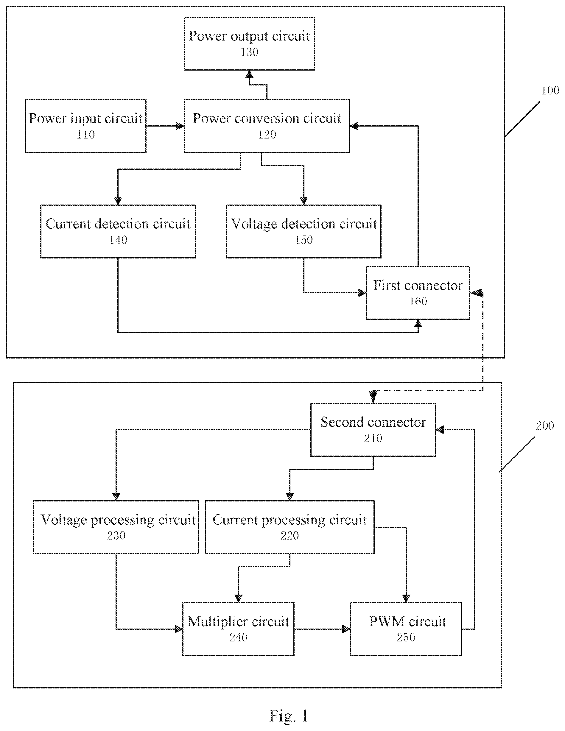
Disclosed are a constant-power supply apparatus and a solar simulation facility. The constant-power supply apparatus comprises: a power board and a control panel, wherein the power board comprises: a power input circuit for providing a power input, a power conversion circuit connected to the power input circuit, a voltage detection circuit, a current detection circuit and a power output circuit respectively connected to the power conversion circuit, and a first connector connected to the power conversion circuit, the voltage detection circuit and the current detection circuit; and the control board comprises: a second connector pluggably connected to the first connector, a voltage processing circuit and a current processing circuit respectively connected to the second connector, a multiplier circuit connected to the voltage processing circuit and the current processing circuit, and a PWM circuit connected to the current processing circuit, the multiplier circuit and the second connector.
Claims (20)
1 . A constant-power supply apparatus, comprising: a power board and a control panel, wherein: the power board comprises: a power input circuit configured for providing a power input, a power conversion circuit connected to the power input circuit, a voltage detection circuit, a current detection circuit and a power output circuit respectively connected to the power conversion circuit, and a first connector connected to the power conversion circuit, the voltage detection circuit and the current detection circuit; and the control panel comprises: a second connector pluggably connected to the first connector, a voltage processing circuit and a current processing circuit respectively connected to the second connector, a multiplier circuit connected to the voltage processing circuit and the current processing circuit, and a PWM circuit connected to the current processing circuit, the multiplier circuit and the second connector.
12 . A solar simulation facility, comprising the constant-power supply apparatus including a power board and a control panel, wherein: the power board comprises: a power input circuit configured for providing a power input, a power conversion circuit connected to the power input circuit, a voltage detection circuit, a current detection circuit and a power output circuit respectively connected to the power conversion circuit, and a first connector connected to the power conversion circuit, the voltage detection circuit and the current detection circuit; and the control panel comprises: a second connector pluggably connected to the first connector, a voltage processing circuit and a current processing circuit respectively connected to the second connector, a multiplier circuit connected to the voltage processing circuit and the current processing circuit, and a PWM circuit connected to the current processing circuit, the multiplier circuit and the second connector.
Show 18 dependent claims
2 . The constant-power supply apparatus according to claim 1 , wherein: the power conversion circuit comprises a switch tube, a photocoupling unit and a Chock inductor, an input terminal of the switch tube is connected to the power input circuit, an output terminal of the switch tube is connected to a first terminal of the Chock inductor, a second terminal of the Chock inductor is connected to the power output circuit, a control terminal of the switch tube is connected to a voltage output terminal of the photocoupling unit, a positive pole of the photocoupling unit is connected to a sixth pin of the first connector, and a negative pole of the photocoupling unit is connected to a first pin of the first connector.
3 . The constant-power supply apparatus according to claim 1 , wherein the voltage detection circuit comprises a voltage dividing circuit, and the voltage processing circuit comprises a first amplifying circuit; a first terminal of the voltage dividing circuit is connected to the power conversion circuit and the power output circuit, a second terminal of the voltage dividing circuit is grounded, and a third terminal of the voltage dividing circuit is connected to a tenth pin of the first connector; and an input terminal of the first amplifying circuit is connected to a tenth pin of the second connector, and an output terminal of the first amplifying circuit is connected to the multiplier circuit.
4 . The constant-power supply apparatus according to claim 3 , wherein the first amplifying circuit comprises a first operational amplifier and a second operational amplifier; a first input terminal of the first operational amplifier is connected to a first input terminal of the second operational amplifier and the first connector, a second input terminal of the first operational amplifier is connected to an output terminal of the first operational amplifier and the multiplier circuit, and a second input terminal of the second operational amplifier is connected to an output terminal of the second operational amplifier.
5 . The constant-power supply apparatus according to claim 1 , wherein the current detection circuit comprises a Hall sensor arranged in the power conversion circuit, and the current processing circuit comprises a first rectifier tube and a second amplifying circuit; an output terminal of the Hall sensor is connected to a third pin of the first connector, a first terminal of the first rectifier tube is connected to an input terminal of the second amplifying circuit, a second terminal of the first rectifier tube is connected to a third pin of the second connector, a third terminal of the first rectifier tube is grounded, and an output terminal of the second amplifying circuit is connected to the multiplier circuit.
6 . The constant-power supply apparatus according to claim 5 , wherein the second amplifying circuit comprises a third operational amplifier and a first variable resistor; a first input terminal of the third operational amplifier is connected to the first rectifier tube and a first terminal of the variable resistor, a second input terminal of the third operational amplifier is grounded, an output terminal of the third operational amplifier is connected to the multiplier circuit and a second terminal and a third terminal of the first variable resistor.
7 . The constant-power supply apparatus according to claim 1 , wherein the multiplier circuit comprises an analog multiplier, a third amplifying circuit, a second rectifier tube and an output current regulation circuit; a first input terminal of the analog multiplier is connected to the voltage processing circuit, a second input terminal of the analog multiplier is connected to the current processing circuit, an output terminal of the analog multiplier is connected to an input terminal of the third amplifying circuit, an output terminal of the third amplifying circuit is connected to a second terminal of the second rectifier tube, and a first terminal of the second rectifier tube is connected to the PWM circuit and the output current regulation circuit.
8 . The constant-power supply apparatus according to claim 7 , wherein the third amplifying circuit comprises a fourth operational amplifier, a fifth operational amplifier, a resistor R 11 , a resistor R 14 , a resistor R 12 , a diode D 3 , a capacitor C 4 and a capacitor C 5 ; a second input terminal of the fourth operational amplifier is connected to an output terminal of the analog multiplier and a first terminal of the resistor R 11 , a second terminal of the resistor R 11 is connected to an output terminal of the fourth operational amplifier and a first terminal of the resistor R 14 , a first input terminal of the fourth operational amplifier is grounded, a second terminal of the resistor R 14 is connected to a first input terminal of the fifth operational amplifier, a positive pole of the diode D 3 , a first terminal of the capacitor C 14 and a first terminal of the resistor R 12 , an output terminal of the fifth operational amplifier is connected to a negative pole of the diode D 3 , a second terminal of the capacitor C 4 and a first terminal of the capacitor C 5 , a second terminal of the capacitor C 5 is connected to a second terminal of the resistor R 12 , and a second input terminal of the fifth operational amplifier is grounded.
9 . The constant-power supply apparatus according to claim 7 , wherein the output current regulation circuit comprises: a diode D 1 , a sixth operational amplifier, a second variable resistor, a resistor R 4 , a capacitor C 14 , a capacitor C 2 and a resistor R 8 ; a positive pole of the diode D 1 is connected to the first terminal of the second rectifier tube, a negative pole of the diode D 1 is connected to an output terminal of the sixth operational amplifier through the resistor R 4 , a first input terminal of the sixth operational amplifier is grounded through the capacitor C 14 , a second input terminal of the sixth operational amplifier is connected to a first terminal of the capacitor C 2 , a first terminal of the resistor R 8 and a third terminal of the second variable resistor, a second terminal of the capacitor C 2 is grounded, a second terminal of the resistor R 8 is connected to a fourth pin of the second connector, a second terminal of the second variable resistor is connected to a sixth pin of the second connector, and a first terminal of the second variable resistor is grounded.
10 . The constant-power supply apparatus according to claim 1 , wherein the power output circuit comprises a bridge inversion output circuit and a third connector; the bridge inversion output circuit comprises a MOS transistor Q 4 , a MOS transistor Q 5 , a MOS transistor Q 6 , a MOS transistor Q 7 , a diode D 19 , a diode D 15 , a diode D 7 and a diode D 8 ; a gate of the MOS transistor Q 4 is connected to a first pin of the third connector, and a source of the MOS transistor Q 4 is connected to a positive pole of the diode D 19 and a second pin of the third connector; a gate of the MOS transistor Q 5 is connected to a third pin of the third connector, a drain of the MOS transistor Q 5 is connected to a source of the MOS transistor Q 4 and a negative pole of the diode D 15 ; a gate of the MOS transistor Q 6 is connected to a fourth pin of the third connector, a source of the MOS transistor Q 6 is connected to a positive pole of the diode D 7 and a fifth pin of the third connector; a gate of the MOS transistor Q 7 is connected to a sixth pin of the third connector, a drain of the MOS transistor Q 7 is connected to a source of the MOS transistor Q 6 and a negative pole of the diode D 8 ; a drain of the MOS transistor Q 4 , a negative pole of the diode D 19 , a drain of the MOS transistor Q 6 and a negative pole of the diode D 7 are respectively connected to a power conversion circuit; and a positive pole of the diode D 15 and a positive pole of the diode D 8 , and a source of the MOS transistor Q 5 and a source of the MOS transistor Q 7 are grounded.
11 . The constant-power supply apparatus according to claim 1 , wherein, the PWM circuit comprises a modulation chip U 4 , a second pin and a sixteenth pin of the modulation chip U 4 are respectively connected to the multiplier circuit, a twelfth pin and a thirteenth pin of the modulation chip U 4 are respectively connected to a first pin of the second connector, a tenth pin of the modulation chip U 4 is connected to a ninth pin of the second connector, and a ninth pin and a first pin of the modulation chip U 4 are respectively connected to the current processing circuit.
13 . The solar simulation facility according to claim 12 , wherein the power conversion circuit comprises a switch tube, a photocoupling unit and a Chock inductor, an input terminal of the switch tube is connected to the power input circuit, an output terminal of the switch tube is connected to a first terminal of the Chock inductor, a second terminal of the Chock inductor is connected to the power output circuit, a control terminal of the switch tube is connected to a voltage output terminal of the photocoupling unit, a positive pole of the photocoupling unit is connected to a sixth pin of the first connector, and a negative pole of the photocoupling unit is connected to a first pin of the first connector.
14 . The solar simulation facility according to claim 12 , wherein the voltage detection circuit comprises a voltage dividing circuit, and the voltage processing circuit comprises a first amplifying circuit; a first terminal of the voltage dividing circuit is connected to the power conversion circuit and the power output circuit, a second terminal of the voltage dividing circuit is grounded, and a third terminal of the voltage dividing circuit is connected to a tenth pin of the first connector; and an input terminal of the first amplifying circuit is connected to a tenth pin of the second connector, and an output terminal of the first amplifying circuit is connected to the multiplier circuit.
15 . The solar simulation facility according to claim 12 , wherein the current detection circuit comprises a Hall sensor arranged in the power conversion circuit, and the current processing circuit comprises a first rectifier tube and a second amplifying circuit; an output terminal of the Hall sensor is connected to a third pin of the first connector, a first terminal of the first rectifier tube is connected to an input terminal of the second amplifying circuit, a second terminal of the first rectifier tube is connected to a third pin of the second connector, a third terminal of the first rectifier tube is grounded, and an output terminal of the second amplifying circuit is connected to the multiplier circuit.
16 . The solar simulation facility according to claim 12 , wherein the multiplier circuit comprises an analog multiplier, a third amplifying circuit, a second rectifier tube and an output current regulation circuit; a first input terminal of the analog multiplier is connected to the voltage processing circuit, a second input terminal of the analog multiplier is connected to the current processing circuit, an output terminal of the analog multiplier is connected to an input terminal of the third amplifying circuit, an output terminal of the third amplifying circuit is connected to a second terminal of the second rectifier tube, and a first terminal of the second rectifier tube is connected to the PWM circuit and the output current regulation circuit.
17 . The solar simulation facility according to claim 16 , wherein the third amplifying circuit comprises a fourth operational amplifier, a fifth operational amplifier, a resistor R 11 , a resistor R 14 , a resistor R 12 , a diode D 3 , a capacitor C 4 and a capacitor C 5 ; a second input terminal of the fourth operational amplifier is connected to an output terminal of the analog multiplier and a first terminal of the resistor R 11 , a second terminal of the resistor R 11 is connected to an output terminal of the fourth operational amplifier and a first terminal of the resistor R 14 , a first input terminal of the fourth operational amplifier is grounded, a second terminal of the resistor R 14 is connected to a first input terminal of the fifth operational amplifier, a positive pole of the diode D 3 , a first terminal of the capacitor C 14 and a first terminal of the resistor R 12 , an output terminal of the fifth operational amplifier is connected to a negative pole of the diode D 3 , a second terminal of the capacitor C 4 and a first terminal of the capacitor C 5 , a second terminal of the capacitor C 5 is connected to a second terminal of the resistor R 12 , and a second input terminal of the fifth operational amplifier is grounded.
18 . The solar simulation facility according to claim 16 , wherein the output current regulation circuit comprises: a diode D 1 , a sixth operational amplifier, a second variable resistor, a resistor R 4 , a capacitor C 14 , a capacitor C 2 and a resistor R 8 ; a positive pole of the diode D 1 is connected to the first terminal of the second rectifier tube, a negative pole of the diode D 1 is connected to an output terminal of the sixth operational amplifier through the resistor R 4 , a first input terminal of the sixth operational amplifier is grounded through the capacitor C 14 , a second input terminal of the sixth operational amplifier is connected to a first terminal of the capacitor C 2 , a first terminal of the resistor R 8 and a third terminal of the second variable resistor, a second terminal of the capacitor C 2 is grounded, a second terminal of the resistor R 8 is connected to a fourth pin of the second connector, a second terminal of the second variable resistor is connected to a sixth pin of the second connector, and a first terminal of the second variable resistor is grounded.
19 . The solar simulation facility according to claim 12 , wherein the PWM circuit comprises a modulation chip U 4 , a second pin and a sixteenth pin of the modulation chip U 4 are respectively connected to the multiplier circuit, a twelfth pin and a thirteenth pin of the modulation chip U 4 are respectively connected to a first pin of the second connector, a tenth pin of the modulation chip U 4 is connected to a ninth pin of the second connector, and a ninth pin and a first pin of the modulation chip U 4 are respectively connected to the current processing circuit.
20 . The solar simulation facility according to claim 12 , wherein the power output circuit comprises a bridge inversion output circuit and a third connector; the bridge inversion output circuit comprises a MOS transistor Q 4 , a MOS transistor Q 5 , a MOS transistor Q 6 , a MOS transistor Q 7 , a diode D 19 , a diode D 15 , a diode D 7 and a diode D 8 ; a gate of the MOS transistor Q 4 is connected to a first pin of the third connector, and a source of the MOS transistor Q 4 is connected to a positive pole of the diode D 19 and a second pin of the third connector; a gate of the MOS transistor Q 5 is connected to a third pin of the third connector, a drain of the MOS transistor Q 5 is connected to a source of the MOS transistor Q 4 and a negative pole of the diode D 15 ; a gate of the MOS transistor Q 6 is connected to a fourth pin of the third connector, a source of the MOS transistor Q 6 is connected to a positive pole of the diode D 7 and a fifth pin of the third connector; a gate of the MOS transistor Q 7 is connected to a sixth pin of the third connector, a drain of the MOS transistor Q 7 is connected to a source of the MOS transistor Q 6 and a negative pole of the diode D 8 ; a drain of the MOS transistor Q 4 , a negative pole of the diode D 19 , a drain of the MOS transistor Q 6 and a negative pole of the diode D 7 are respectively connected to a power conversion circuit; and a positive pole of the diode D 15 and a positive pole of the diode D 8 , and a source of the MOS transistor Q 5 and a source of the MOS transistor Q 7 are grounded.
Full Description
Show full text →
BACKGROUND OF THE INVENTION
1. Technical Field The invention relates to the technical field of driving power, and particularly to a constant-power supply apparatus and a solar simulation facility. 2. Description of Related Art Solar simulation test facilities typically use a HQI discharge bulb of OSRAM as a light source to test ultraviolet parameters. With the long-term use of the bulb, the resistance of a circuit in the bulb will increase, and the voltage of the bulb rises accordingly during use. Because the variation of the operating voltage of a stable current drive device of the circuit will lead to a continuous change of power in the working process of a lamp, the instability of the power will affect the light-emitting parameters and life of the bulb. BRIEF
SUMMARY OF THE INVENTION
The technical issue to be settled by the invention is to overcome the above-mentioned defects of the prior art to provide a constant-power supply apparatus and a solar simulation facility. The technical solution adopted by the invention to settle the technical issue is as follows: a constant-power supply apparatus is provided and comprises: a power board and a control panel, wherein: The power board comprises: a power input circuit for providing a power input, a power conversion circuit connected to the power input circuit, a voltage detection circuit, a current detection circuit and a power output circuit respectively connected to the power conversion circuit, and a first connector connected to the power conversion circuit, the voltage detection circuit and the current detection circuit; The control panel comprises: a second connector pluggably connected to the first connector, a voltage processing circuit and a current processing circuit respectively connected to the second connector, a multiplier circuit connected to the voltage processing circuit and the current processing circuit, and a PWM (Pulse Width Modulation) circuit connected to the current processing circuit, the multiplier circuit and the second connector. Preferably, The power conversion circuit comprises a switch tube, a photocoupling unit and a Chock inductor, wherein an input terminal of the switch tube is connected to the power input circuit, an output terminal of the switch tube is connected to a first terminal of the Chock inductor, a second terminal of the Chock inductor is connected to the power output circuit, a control terminal of the switch tube is connected to a voltage output terminal of the photocoupling unit, a positive pole of the photocoupling unit is connected to a sixth pin of the first connector, and a negative pole of the photocoupling unit is connected to a first pin of the first connector. Preferably, The voltage detection circuit comprises a voltage dividing circuit, and the voltage processing circuit comprises a first amplifying circuit; A first terminal of the voltage dividing circuit is connected to the power conversion circuit and the power output circuit, a second terminal of the voltage dividing circuit is grounded, and a third terminal of the voltage dividing circuit is connected to a tenth pin of the first connector; An input terminal of the first amplifying circuit is connected to a tenth pin of the second connector, and an output terminal of the first amplifying circuit is connected to the multiplier circuit. Preferably, The first amplifying circuit comprises a first operational amplifier and a second operational amplifier; A first input terminal of the first operational amplifier is connected to a first input terminal of the second operational amplifier and the first connector, a second input terminal of the first operational amplifier is connected to an output terminal of the first operational amplifier and the multiplier circuit, and a second input terminal of the second operational amplifier is connected to an output terminal of the second operational amplifier. Preferably, The current detection circuit comprises a Hall sensor arranged on the current conversion circuit, and the current processing circuit comprises a first rectifier tube and a second amplifying circuit; An output terminal of the Hall sensor is connected to a third pin of the first connector, a first terminal of the first rectifier tube is connected to an input terminal of the second amplifying circuit, a second terminal of the first rectifier tube is connected to a third pin of the second connector, a third terminal of the first rectifier tube is grounded, and an output terminal of the second amplifying circuit is connected to the multiplier circuit. Preferably, The second amplifying circuit comprises a third operational amplifier and a first variable resistor; A first input terminal of the third operational amplifier is connected to the first rectifier tube and a first terminal of the variable resistor, a second input terminal of the third operational amplifier is grounded, an output terminal of the third operational amplifier is connected to the multiplier circuit and a second terminal and a third terminal of the first variable resistor. Preferably, The multiplier circuit comprises an analog multiplier, a third amplifying circuit, a second rectifier tube and an output current regulation circuit; A first input terminal of the analog multiplier is connected to the voltage processing circuit, a second input terminal of the analog multiplier is connected to the current processing circuit, an output terminal of the analog multiplier is connected to an input terminal of the third amplifying circuit, an output terminal of the third amplifying circuit is connected to a second terminal of the second rectifier tube, and a first terminal of the second rectifier tube is connected to the PWM circuit and the output current regulation circuit; and/or The PWM circuit comprises a modulation chip U 4 , wherein a second pin and a sixteenth pin of the modulation chip U 4 are connected to the multiplier circuit, a twelfth pin and a thirteenth pin of the modulation chip U 4 are connected to a first pin of the second connector, a tenth pin of the modulation chip U 4 is connected to a ninth pin of the second connector, and a ninth pin and a first pin of the modulation chip U 4 are connected to the current processing circuit. Preferably, The third amplifying circuit comprises a fourth operational amplifier, a fifth operational amplifier, a resistor R 11 , a resistor R 14 , a resistor R 12 , a diode D 3 , a capacitor C 4 and a capacitor C 5 ; A second input terminal of the fourth operational amplifier is connected to an output terminal of the analog multiplier and a first terminal of the resistor R 11 , a second terminal of the resistor R 11 is connected to an output terminal of the fourth operational amplifier and a first terminal of the resistor R 14 , a first input terminal of the fourth operational amplifier is grounded, a second terminal of the resistor R 14 is connected to a first input terminal of the fifth operational amplifier, a positive pole of the diode D 3 , a first terminal of the capacitor C 14 and a first terminal of the resistor R 12 , an output terminal of the fifth operational amplifier is connected to a negative pole of the diode D 3 , a second terminal of the capacitor C 4 and a first terminal of the capacitor C 5 , a second terminal of the capacitor C 5 is connected to a second terminal of the resistor R 12 , and a second input terminal of the fifth operational amplifier is grounded; and/or The output current regulation circuit comprises: a diode D 1 , a sixth operational amplifier, a second variable resistor, a resistor R 4 , a capacitor C 14 , a capacitor C 2 and a resistor R 8 ; A positive pole of the diode D 1 is connected to the first terminal of the second rectifier tube, a negative pole of the diode D 1 is connected to an output terminal of the sixth operational amplifier through the resistor R 4 , a first input terminal of the sixth operational amplifier is grounded through the capacitor C 14 , a second input terminal of the sixth operational amplifier is connected to a first terminal of the capacitor C 2 , a first terminal of the resistor R 8 and a third terminal of the second variable resistor, a second terminal of the capacitor C 2 is grounded, a second terminal of the resistor R 8 is connected to a fourth pin of the second connector, a second terminal of the second variable resistor is connected to a sixth pin of the second connector, and a first terminal of the second variable resistor is grounded. Preferably, The power output circuit comprises a bridge inversion output circuit and a third connector; The bridge inversion output circuit comprises a MOS transistor Q 4 , a MOS transistor Q 5 , a MOS transistor Q 6 , a MOS transistor Q 7 , a diode D 19 , a diode D 15 , a diode D 7 and a diode D 8 ; A gate of the MOS transistor Q 4 is connected to a first pin of the third connector, and a source of the MOS transistor Q 4 is connected to a positive pole of the diode D 19 and a second pin of the third connector; a gate of the MOS transistor Q 5 is connected to a third pin of the third connector, a drain of the MOS transistor Q 5 is connected to a source of the MOS transistor Q 4 and a negative pole of the diode D 15 , a gate of the MOS transistor Q 6 is connected to a fourth pin of the third connector, a source of the MOS transistor Q 6 is connected to a positive pole of the diode D 7 and a fifth pin of the third connector, a gate of the MOS transistor Q 7 is connected to a sixth pin of the third connector, a drain of the MOS transistor Q 7 is connected to a source of the MOS transistor Q 6 and a negative pole of the diode D 8 , a drain of the MOS transistor Q 4 , a negative pole of the diode D 19 , a drain of the MOS transistor Q 6 and a negative pole of the diode D 7 are respectively connected to a power conversion circuit, a positive pole of the diode D 15 and a positive pole of the diode D 8 , and a source of the MOS transistor Q 5 and a source of the MOS transistor Q 7 are grounded. The invention further provides a solar simulation facility, comprising any one constant-power supply apparatus mentioned above. The constant-power supply apparatus and the solar simulation device have the following beneficial effects: a stable power output can be provided, and the reliability of circuit is guaranteed. BRIEF DESCRIPTION OF THE SEVERAL VIEWS OF THE DRAWINGS The invention will be further described below in conjunction with accompanying drawings and embodiments. In the figures: is a structural diagram of a constant-power supply apparatus of the invention; is a schematic circuit diagram of one embodiment of a power board in the constant-power supply apparatus of the invention; is a schematic circuit diagram of one embodiment of a control panel in the constant-power supply apparatus of the invention.
DETAILED DESCRIPTION
OF THE INVENTION To gain a better understanding of the technical features, purposes and effects of the invention, specific embodiments of the invention will be explained in detail below with reference to the accompanying drawings. As shown in , in a first embodiment of the invention, a constant-power supply apparatus comprises a power board 100 and a control panel 200 . The power board 100 comprises: a power input circuit 110 configured for providing a power input, a power conversion circuit 120 connected to the power input circuit 110 , a voltage detection circuit 150 , a current detection circuit 140 and a power output circuit 130 respectively connected to the power conversion circuit 120 , and a first connector 160 connected to the power conversion circuit 120 , the voltage detection circuit 150 and the current detection circuit 140 . The control panel 200 comprises a second connector 210 pluggably connected to the first connector 160 , a voltage processing circuit 230 and a current processing circuit 220 respectively connected to the second connector 210 , a multiplier circuit 240 connected to the voltage processing circuit 230 and the current processing circuit 220 , and a PWM circuit 250 connected to the current processing circuit 220 , the multiplier circuit 240 and the second connector 210 . Specifically, the constant-power supply apparatus comprises the power board 100 and the control panel 200 , wherein the power board 100 and the control panel 200 are pluggably connected through the first connector 160 and the second connector 210 . The power board 100 is configured for carrying out voltage conversion on the power input of the power input circuit 110 through the power conversion circuit 120 and then providing a power output through the power output circuit to provide operating power for a subsequent operating circuit. The power board 100 is provided with the voltage detection circuit 150 for detecting an output voltage of the power conversion circuit 120 and the current detection circuit 140 for detecting an output current of the power conversion circuit 120 . A voltage detection signal corresponding to the output voltage and a current detection signal corresponding to the output current are input to the control panel 200 through the first connector 160 and the second connector 210 , respectively. The control panel 200 is provided with the voltage processing circuit 230 corresponding to the voltage detection signal and the current processing circuit 220 corresponding to the current detection signal, the voltage detection signal and the current detection signal are processed by the voltage processing circuit 230 and the current processing circuit 220 and are then sent to the multiplier circuit 240 which acquires corresponding output power based on the voltage detection signal and the current detection signal and outputs a corresponding trigger signal based on the output power. The PWM circuit 250 acquires the trigger signal and the current detection signal processed by the current processing circuit 220 and is triggered by the trigger signal corresponding to the current detection signal to output a PWM signal, whereby the power conversion circuit 120 is controlled by the PWM signal to work and to output stable power. As shown in , the power conversion circuit 120 comprises a switch tube, a photocoupling unit and a Chock inductor, wherein an input terminal of the switch tube is connected to the power input circuit 110 , an output terminal of the switch tube is connected to a first terminal of the Chock inductor, a second terminal of the Chock inductor is connected to the power output circuit, a control terminal of the switch tube is connected to a voltage output terminal of the photocoupling unit, a positive pole of the photocoupling unit is connected to a sixth pin of the first connector 160 , and a negative pole of the photocoupling unit is connected to a first pin of the first connector 160 . Specifically, in the power conversion circuit 120 , the PWM signal output by the control panel 200 controls on or off of a positive pole and a negative pole of a light-emitting tube in the photocoupling unit to control on or off of a photosensitive tube in the photocoupling unit to finally control on or off of the switch tube, such that a final power output of the power conversion circuit 120 is controlled. Wherein, the photocoupling unit receives the PWM signal from the control panel 200 through the first pin of the first connector 160 . Wherein, the switch tube comprises an MOS transistor Q 3 , the photocoupling unit comprises a photocoupler U 2 , the first connector 160 may be a 10PIN connector J 4 , a source of the MOS transistor Q 3 is connected to the Chock inductor L 1 , and a gate of the MOS transistor Q 3 is connected to a photosensitive output terminal of the photocoupler U 2 through a resistor R 17 . Optionally, as shown in and , the voltage detection circuit 150 comprises a voltage dividing circuit, and the voltage processing circuit 230 comprises a first amplifying circuit; a first terminal of the voltage dividing circuit is connected to the power conversion circuit 120 and the power output circuit 130 , a second terminal of the voltage dividing circuit is grounded, and a third terminal of the voltage dividing circuit is connected to a tenth pin of the first connector 160 ; and an input terminal of the first amplifying circuit is connected to a tenth pin of the second connector 210 , and an output terminal of the first amplifying circuit is connected to the multiplier circuit 240 . Specifically, the voltage detection circuit 150 adopts the voltage dividing circuit for voltage detection, and the voltage dividing circuit may comprise a resistor R 30 , a resistor R 35 and a resistor R 34 , wherein after being connected in series, the resistor R 30 and the resistor R 35 have one terminal connected to the power conversion circuit and the power output circuit 130 and the other terminal connected to a first terminal of the resistor R 34 and the tenth pin of the first connector 160 , the other terminal of the resistor R 34 is grounded, and the voltage detection signal corresponding to the output voltage of the power conversion circuit is obtained through voltage division of the resistor R 34 . Wherein, the voltage detection signal is filtered by a capacitor C 31 connected in parallel with the resistor R 34 . In the voltage processing circuit 230 , the voltage detection signal is amplified by the first amplifying circuit, that is, the input terminal of the first amplifying circuit is connected to the tenth pin of the second connector 210 , and the first amplifying circuit acquires the voltage detection signal through the tenth pin of the first connector 160 . After being amplified, the voltage detection signal is sent to the multiplier circuit 240 for corresponding operation. The second connector 210 may be a 10PIN connector J 1 . Optionally, the first amplifying circuit comprises a first operational amplifier U 5 -B and a second operational amplifier U 5 -A, wherein a first input terminal of the first operational amplifier U 5 -B is connected to a first input terminal of the second operational amplifier U 5 -A and the first connector 160 , a second input terminal of the first operational amplifier U 5 -B is connected to an output terminal of the first operational amplifier U 5 -B and the multiplier circuit 240 , and a second input terminal of the second operational amplifier U 5 -A is connected to an output terminal of the second operational amplifier U 5 -A. Specifically, the first amplifying circuit may be a follower amplifying circuit and adopts two operational amplifiers, namely the first operational amplifier U 5 -B and the second operational amplifier U 5 -A, the voltage detection signal is amplified by means of follower amplification realized by such a connection relation, and the amplified voltage detection signal is sent to the multiplier circuit 240 through the output terminal of the first operational amplifier U 5 -B. Optionally, the current detection circuit 140 comprises a Hall sensor arranged on the power conversion circuit 120 , and the current processing circuit 220 comprises a first rectifier tube D 1 and a second amplifying circuit; an output terminal of the Hall sensor is connected to a third pin of the first connector 160 , a first terminal of the first rectifier tube D 1 is connected to an input terminal of the second amplifying circuit, a second terminal of the first rectifier tube D 1 is connected to a third pin of the second connector 210 , a third terminal of the first rectifier tube D 1 is grounded, and an output terminal of the second amplifying circuit is connected to the multiplier circuit 240 . Specifically, a wire for arranging the Hall sensor is reserved at a corresponding position of the power conversion circuit, and the Hall sensor is disposed around the wire and is mechanically connected to the wire. The Hall sensor detects an induction current generated when a current passes through the wire, that it, a corresponding current detection signal is generated; and the current detection signal is input to the control panel 200 through the third pin of the first connector 160 . In the control panel 200 , the current processing circuit 220 comprises the first rectifier tube D 1 and the second amplifying circuit and rectifies the current detection signal through the second rectifier tube D 1 , and after being rectified, the current detection signal is amplified by the second amplifying circuit and is sent to the analog multiplier circuit 240 to be processed correspondingly. Optionally, the second amplifying circuit comprises a third operational amplifier U 2 -A and a first variable resistor PR 1 , wherein a first input terminal of the third operational amplifier U 2 -A is connected to the first rectifier tube D 1 and a first terminal of the first variable resistor PR 1 , a second input terminal of the third operational amplifier U 2 -A is grounded, and an output terminal of the third operational amplifier U 2 -A is connected to the multiplier circuit 240 and a second terminal and a third terminal of the first variable resistor PR 1 . Specifically, the second amplifying circuit amplifies the current detection signal through the third operational amplifier U 2 -A, wherein the first input terminal of the third operational amplifier U 2 -A is connected to the first terminal of the first variable resistor PR 2 through a resistor R 3 , the output terminal of the third operational amplifier U 2 -A is connected to the second terminal and the third terminal of the first variable resistor PR 1 , and the amplification factor of the third operational amplifier U 2 -A can be changed by adjusting the first variable resistor PR 1 to finally regulate the current output. Optionally, the multiplier circuit 240 comprises an analog multiplier 241 , a third amplifying circuit 242 , a second rectifier tube 243 and an output current regulation circuit 244 , wherein a first input terminal of the analog multiplier 241 is connected to the voltage processing circuit 230 , a second input terminal of the analog multiplier 241 is connected to the current processing circuit 220 , an output terminal of the analog multiplier 241 is connected to an input terminal of the third amplifying circuit 242 , an output terminal of the third amplifying circuit 242 is connected to a second terminal of the second rectifier tube 243 , and a first terminal of the second rectifier tube 243 is connected to the PWM circuit 250 and the output current regulation circuit 244 . Specifically, the multiplier circuit 240 may comprise an analog multiplier 241 and may adopt an analog multiplier chip U 3 , wherein a first pin, corresponding to the first input terminal, of the analog multiplier chip U 3 is connected to the voltage processing circuit 230 through a resistor R 42 , an eighth pin, corresponding to the second input terminal, of the analog multiplier chip U 3 is connected to the current processing circuit 220 through a resistor R 39 , a fourth pin, corresponding to the output terminal, of the analog multiplier chip U 3 is connected to the input terminal of the third amplifying circuit 242 , the current detection signal and the voltage detection signal are multiplied by the analog multiplier chip U 3 to obtain a power monitoring signal corresponding to the output power of the power conversion circuit 120 , the power monitoring signal is amplifier by the third amplifying circuit 242 and is rectified by the second rectifier tube 243 to obtain a corresponding trigger signal, and the PWM circuit 250 is triggered by the trigger signal. Wherein, the second rectifier tube 243 may be a rectifier tube D 5 , the multiplier circuit 240 detects a current corresponding to the trigger signal output by the rectifier tube D 5 , and the current corresponding to the trigger signal is regulated by the output current regulation circuit, so that the PWM circuit 250 can recognize the trigger signal. A closed-loop system capable of realizing monitoring is formed by this circuit, the load power of a load circuit such as a light source varies along with the service time of the circuit when the load circuit works, and the power can be automatically stabilized by the regulation system by means of current detection. Wherein, the analog multiplier chip U 3 may be a multiplier RC 4200 . Optionally, the PWM circuit 250 comprises a modulation chip U 4 , wherein a second pin and a sixteenth pin of the modulation chip U 4 are respectively connected to the multiplier circuit 240 , a twelfth pin and a thirteenth pin of the modulation chip U 4 are respectively connected to a first pin of the second connector 210 , a tenth pin of the modulation chip U 4 is connected to a ninth pin of the second connector 210 , and a ninth pin and a first pin of the modulation chip U 4 are respectively connected to the current processing circuit 220 . The PWM circuit 250 may adopt the modulation chip U 4 , the modulation chip U 4 may be a UC 2524 chip, the second pin and the sixteenth pin of the modulation chip U 4 are respectively connected to the multiplier circuit 240 , wherein the second pin is used for receiving a trigger signal output by the multiplier circuit 240 , the sixteenth pin is used for acquiring a reference voltage according to the trigger signal, the modulation chip U 4 works according to the reference voltage, outputs a PWM signal through the twelfth pin and the thirteenth pin and outputs the PWM signal to the power board 100 through the first pin of the second connector 210 , the tenth pin of the modulation chip U 4 is connected to the ninth pin of the second connector 210 to receive a starting signal, and the starting signal is a ballast starting signal or a circuit work starting signal and is generally a high or low level. The ninth pin and the first pin of the modulation chip U 4 are respectively connected to the current processing circuit 220 and are used for receiving a voltage signal, and the voltage is high when the current is large. Optionally, the third amplifying circuit comprises a fourth operational amplifier U 2 -D, a fifth operational amplifier U 2 -C, a resistor R 11 , a resistor R 14 , a resistor R 12 , a diode D 3 , a capacitor C 4 and a capacitor C 5 , wherein a second input terminal of the fourth operational amplifier U 2 -D is connected to an output terminal of the analog multiplier and a first terminal of the resistor R 11 , a second terminal of the resistor R 11 is connected to an output terminal of the fourth operational amplifier U 2 -D and a first terminal of the resistor R 14 , a first input terminal of the fourth operational amplifier U 2 -D is grounded, a second terminal of the resistor R 14 is connected to a first input terminal of the fifth operational amplifier U 2 -C, a positive pole of the diode D 3 , a first terminal of the capacitor C 14 and a first terminal of the resistor R 12 , an output terminal of the fifth operational amplifier U 2 -C is connected to a negative pole of the diode D 3 , a second terminal of the capacitor C 4 and a first terminal of the capacitor C 5 , a second terminal of the capacitor C 5 is connected to a second terminal of the resistor R 12 , and a second input terminal of the fifth operational amplifier U 2 -C is grounded; an output signal of the analog multiplier is amplified by a third amplifying circuit composed of the fourth operational amplifier U 2 -D and the fifth operational amplifier U 2 -C to ensure that a trigger signal output by the multiplier circuit 240 meets requirements of the PWM circuit 250 . The specific circuit connection relation has been described above. Wherein, the first input terminal of the fifth operational amplifier U 2 -C is grounded through a diode D 2 -A, a positive electrode of the diode D 2 -A is grounded, and a negative pole of the diode D 2 -A is connected to the first input terminal of the fifth operational amplifier U 2 -C. Optionally, the output current regulation circuit comprises a diode D 1 , a sixth operational amplifier U 2 -B, a second variable resistor VR 1 , a resistor R 4 , a capacitor C 14 , a capacitor C 12 and a resistor R 8 , wherein a positive pole of the diode D 1 is connected to a first terminal of the second rectifier tube D 5 , a negative pole of the diode D 1 is connected to an output terminal of the sixth operational amplifier U 2 -B through the resistor R 4 , a first input terminal of the sixth operational amplifier U 2 -B is grounded through the capacitor C 14 , a second input terminal of the sixth operational amplifier U 2 -B is connected to a first terminal of the capacitor C 2 , a first terminal of the resistor R 8 and a third terminal of the second variable resistor VR 1 , a second terminal of the capacitor C 2 is grounded, a second terminal of the resistor R 8 is connected to a fourth pin of the second connector 210 , a second terminal of the second variable resistor VR 1 is connected to a sixth pin of the second connector 210 , and a first terminal of the second variable resistor VR 1 is grounded. The output current regulation circuit forms a differential amplifier through a DIMMER voltage and a voltage corresponding to the detection current. Optionally, the power output circuit 130 comprises a bridge inversion output circuit and a third connector; The bridge inversion output circuit comprises a MOS transistor Q 4 , a MOS transistor Q 5 , a MOS transistor Q 6 , a MOS transistor Q 7 , a diode D 19 , a diode D 15 , a diode D 7 and a diode D 8 , wherein a gate of the MOS transistor Q 4 is connected to a first pin of the third connector, and a source of the MOS transistor Q 4 is connected to a positive pole of the diode D 19 and a second pin of the third connector; a gate of the MOS transistor Q 5 is connected to a third pin of the third connector, a drain of the MOS transistor Q 5 is connected to a source of the MOS transistor Q 4 and a negative pole of the diode D 15 , a gate of the MOS transistor Q 6 is connected to a fourth pin of the third connector, a source of the MOS transistor Q 6 is connected to a positive pole of the diode D 7 and a fifth pin of the third connector, a gate of the MOS transistor Q 7 is connected to a sixth pin of the third connector, a drain of the MOS transistor Q 7 is connected to a source of the MOS transistor Q 6 and a negative pole of the diode D 8 , a drain of the MOS transistor Q 4 , a negative pole of the diode D 19 , a drain of the MOS transistor Q 6 and a negative pole of the diode D 7 are respectively connected to a power conversion circuit, a positive pole of the diode D 15 and a positive pole of the diode D 8 , and a source of the MOS transistor Q 5 and a source of the MOS transistor Q 7 are grounded. The bridge inversion output circuit provides a stable power output for a subsequent working circuit which may be a light-emitting unit. In addition, the invention provides a solar simulation facility, comprising any one constant-power supply apparatus mentioned above. The constant-power supply apparatus provides a stable power output for a light-emitting unit in the solar simulation facility. It can be understood that the above embodiments are merely preferred ones of the invention and are specifically described in detail, but these embodiments should not be construed as limitations of the scope of the patent of invention. It should be noted that all free combinations of the above technical features and different transformations and improvements made by those ordinarily skilled in the art without departing from the conception of the invention should also fall within the protection scope of the invention. Thus, all equivalent transformations and modifications made within the scope of the claims of the invention should also be under the coverage of the claims of the invention.
Figures (3)
Citations
This patent cites (5)
- US7372241
- US2006/0244426
- US2012/0049761
- US101309047
- US105071657