Rectifier Circuit and Power Supply Using Same
Abstract
A first MOSFET, a second MOSFET, a first control circuit, and a second control circuit are provided; the second MOSFET is in a non-rectification period when the first MOSFET is in a rectification period; the first MOSFET is in a non-rectification period when the second MOSFET is in a rectification period; the first control circuit outputs a voltage generated on the basis of a first input voltage as a first output voltage between the gate and the source of the first MOSFET in at least a portion of a period in which a voltage between the drain and the source of the second MOSFET is inputted as the first input voltage and a negative voltage is applied between the drain and the source of the first MOSFET; the second control circuit outputs a voltage generated on the basis of a second input voltage as a second output voltage between the gate and the source of the second MOSFET in at least a portion of a period in which a voltage between the drain and the source of the first MOSFET is inputted as the second input voltage and a negative voltage is applied between the drain and the source of the second MOSFET.
Claims (12)
1 . A rectifier circuit comprising: a first MOSFET; a second MOSFET; a first control circuit; and a second control circuit, wherein the second MOSFET falls in a non-rectification time period when the first MOSFET falls in a rectification time period, and the first MOSFET falls in a non-rectification time period when the second MOSFET falls in a rectification time period, during at least a part of a time period within which a voltage between a drain and a source of the second MOSFET is inputted as a first input voltage to the first control circuit, and a negative voltage is applied between a drain and a source of the first MOSFET, the first control circuit outputs a voltage generated based on the first input voltage, as a first output voltage, between a gate and the source of the first MOSFET, during at least a part of a time period within which a voltage between the drain and the source of the first MOSFET is inputted as a second input voltage to the second control circuit, and a negative voltage is applied between the drain and the source of the second MOSFET, the second control circuit outputs a voltage generated based on the second input voltage, as a second output voltage, between a gate and the source of the second MOSFET, the first control circuit clamps the first output voltage at a predetermined first threshold voltage when the first input voltage is a voltage equal to or larger than the first threshold voltage, and the second control circuit clamps the second output voltage at a predetermined second threshold voltage when the second input voltage is a voltage equal to or larger than the second threshold voltage.
Show 11 dependent claims
2 . The rectifier circuit according to claim 1 , wherein the first control circuit outputs the first input voltage as the first output voltage when the first input voltage is a voltage smaller than the first threshold voltage, and the second control circuit outputs the second input voltage as the second output voltage when the second input voltage is a voltage smaller than the second threshold voltage.
3 . The rectifier circuit according to claim 1 , wherein the first control circuit includes a third MOSFET including: a drain adapted to receive the first input voltage as an input, a source connected to the gate of the first MOSFET; and a gate connected to the source of the third MOSFET itself with a first resistance interposed therebetween, and further connected to the source of the first MOSFET with a second resistance interposed therebetween, and the second control circuit includes a fourth MOSFET including: a drain adapted to receive the second input voltage as an input, a source connected to the gate of the second MOSFET; and a gate connected to the source of the fourth MOSFET itself with a third resistance interposed therebetween, and further connected to the source of the second MOSFET with a fourth resistance interposed therebetween.
4 . The rectifier circuit according to claim 1 , wherein the first output voltage is a voltage smaller than a maximum value of a drain-source voltage of the second MOSFET, and the second output voltage is a voltage smaller than a maximum value of a drain-source voltage of the first MOSFET.
5 . The rectifier circuit according to claim 1 , wherein the first MOSFET and the second MOSFET comprise N-channel MOSFETs having respective sources connected to a DC low-voltage terminal.
6 . The rectifier circuit according to claim 1 , wherein the first MOSFET and the second MOSFET comprise P-channel MOSFETs having respective sources connected to a DC high-voltage terminal.
7 . The rectifier circuit according to claim 1 , wherein the rectifier circuit has a bridge structure, the first MOSFET and the second MOSFET in a DC low-voltage terminal side comprise N-channel MOSFETs having respective sources connected to a DC low-voltage terminal, and the first MOSFET and the second MOSFET in a DC high-voltage terminal side are P-channel MOSFETs having respective sources connected to a DC high-voltage terminal.
8 . The rectifier circuit according to claim 1 , wherein the first control circuit includes a first switch for clamping the first output voltage at the first threshold voltage when the first input voltage is a voltage equal to or larger than the first threshold voltage, and the second control circuit includes a second switch for clamping the second output voltage at the second threshold voltage when the second input voltage is a voltage equal to or larger than the second threshold voltage.
9 . The rectifier circuit according to claim 1 , wherein the first control circuit includes a first comparator and a first gate driver for controlling a time period during which the first output voltage is generated, and the second control circuit includes a second comparator and a second gate driver for controlling a time period during which the second output voltage is generated.
10 . The rectifier circuit according to claim 9 , wherein the first control circuit includes a first capacitor for stabilizing a voltage at a power supply terminal for the first comparator and the first gate driver, and the second control circuit includes a second capacitor for stabilizing a voltage at a power supply terminal for the second comparator and the second gate driver.
11 . The rectifier circuit according to claim 1 , wherein the rectifier circuit is incorporated in a single semiconductor package.
12 . A power supply using the rectifier circuit according to claim 1 .
Full Description
Show full text →
TECHNICAL FIELD
The present invention relates to structures of rectifier circuits and power supplies using the same, and particularly relates to effective techniques applicable to rectifier circuits for performing synchronous rectification using rectifying MOSFETs.
BACKGROUND
ART General rectifier circuits have employed synchronous rectification through diodes and MOSFETs, in order to rectify alternating currents to direct currents. Rectification using a diode has a problem of a larger loss due to the voltage drop caused by the built-in potential of the diode. On the other hand, synchronous rectification using a MOSFET induces a lower loss, since the MOSFET has no built-in potential and a forward current rises from 0 V. Therefore, in order to attain rectification with a lower loss, synchronous rectification with MOSFETs has been mainly utilized. As a background art in the present technical field, for example, there is a technique as in PTL 1. PTL 1 discloses a rectifier circuit having a bridge structure for realizing synchronous rectification. The rectifier circuit mainly includes rectifying MOSFETs and control circuits. The control circuits include a drive circuit for driving the rectifying MOSFET, a capacitor for supplying power to the drive circuit, a charging control circuit for controlling the charging of the capacitor, and a MOSFET inserted between the charging control circuit and a drain of the rectifying MOSFET ( ). Further, PTL 2 discloses a rectifier circuit capable of achieving synchronous rectification without using a capacitor. In this rectifier circuit, the drain-source voltage of a rectifying MOSFET (233) is divided by resistances (171, 172), and the voltage resulted from the voltage division is inputted as a gate-source voltage of another rectifying MOSFET (183) having a source in common with the former rectifying MOSFET (233) ( ). CITATION LIST Patent Literatures PTL 1: U.S. Pat. No. 10,756,645 PTL 2: JP 2005-295627 A
SUMMARY
OF INVENTION Technical Problem In the rectifier circuit in PTL 1, the capacitor is charged using the voltage applied between the drain and the source of the rectifying MOSFET during off time-periods for the rectifying MOSFET, while a gate-source voltage of the rectifying MOSFET is generated using the voltage across the capacitor during on time periods for the rectifying MOSFET. Therefore, the capacitor is required to have a capacitance, in order that the capacitor holds a desired voltage during the time periods within which the capacitor is not charged. The volume of the power supply capacitor has hindered downsizing and cost reduction of the rectifier circuit. In the rectifier circuit in Patent Document 2, the waveform of the gate-source voltage of the rectifying MOSFET (183) is a waveform resulted from the voltage division through the resistances, which is applied to the waveform of the drain-source voltage of the rectifying MOSFET (233). For example, in a case of rectifying a sinusoidal voltage, the gate-source voltage of the rectifying MOSFET (183) also has a sinusoidal shape, and the gate-source voltage raises and falls slowly, which has induced the problem of deterioration of the loss reduction effect of synchronous rectification. For coping therewith, it is an object of the present invention to provide a rectifier circuit for performing synchronous rectification using rectifying MOSFETs, and a power supply using the same, such that the rectifier circuit enables reducing the capacitance and the volume of a capacitor which supplies power for controlling the rectifying MOSFETs while maintaining the loss reduction effect of the synchronous rectification. Solution to Problem In order to overcome the aforementioned problem, according to the present invention, there is provided a rectifier circuit including: a first MOSFET; a second MOSFET; a first control circuit; and a second control circuit, wherein the second MOSFET falls in a non-rectification time period when the first MOSFET falls in a rectification time period, and the first MOSFET falls in a non-rectification time period when the second MOSFET falls in a rectification time period, and during at least a part of a time period within which a voltage between a drain and a source of the second MOSFET is inputted as a first input voltage to the first control circuit, and a negative voltage is applied between a drain and a source of the first MOSFET, the first control circuit outputs a voltage generated based on the first input voltage, as a first output voltage, between a gate and the source of the first MOSFET, and during at least a part of a time period within which a voltage between the drain and the source of the first MOSFET is inputted as a second input voltage to the second control circuit, and a negative voltage is applied between the drain and the source of the second MOSFET, the second control circuit outputs a voltage generated based on the second input voltage, as a second output voltage, between a gate and the source of the second MOSFET, and the first control circuit clamps the first output voltage at a predetermined first threshold voltage when the first input voltage is a voltage equal to or larger than the first threshold voltage, and the second control circuit clamps the second output voltage at a predetermined second threshold voltage when the second input voltage is a voltage equal to or larger than the second threshold voltage. Advantageous Effects of Invention With the present invention, it is possible to provide a rectifier circuit for performing synchronous rectification using rectifying MOSFETs, and a power supply using the same, wherein the rectifier circuit enables reducing the capacitance and the volume of a capacitor which supplies power for controlling the rectifying MOSFETS while maintaining the loss reduction effect of the synchronous rectification. Consequently, it is possible to achieve efficiency increase, downsizing, and cost reduction of the rectifier circuit and the power supply using the same. Other problems, structures and effects than those described above will be clarified by the following description of embodiments.
BRIEF DESCRIPTION OF DRAWINGS
is a view illustrating the structure of a rectifier circuit in a first embodiment of the present invention. is a diagram illustrating waveforms rectified by the rectifier circuit of . is a view illustrating the structure of a rectification bridge to which the rectifier circuit of is applied. is a view illustrating the structure of a rectifier circuit in a second embodiment of the present invention. is a view illustrating the structure of a rectifier circuit in a third embodiment of the present invention. is a view illustrating the structure of a rectification bridge in the third embodiment of the present invention. is a view illustrating the structure of a rectifier circuit in a fourth embodiment of the present invention. is a view illustrating the structure of a rectifier circuit in a modification embodiment of the fourth embodiment of the present invention. is a view illustrating the structure of a semiconductor package in a fifth embodiment of the present invention. is a view illustrating the structure of a front-end power supply in a sixth embodiment of the present invention. is a view illustrating the structure of a rectifier circuit in a comparative embodiment 1. is a diagram illustrating waveforms rectified by the rectifier circuit of . is a view illustrating the structure of a rectifier circuit in a comparative embodiment 2. is a diagram illustrating waveforms rectified by the rectifier circuit of .
DESCRIPTION OF EMBODIMENTS
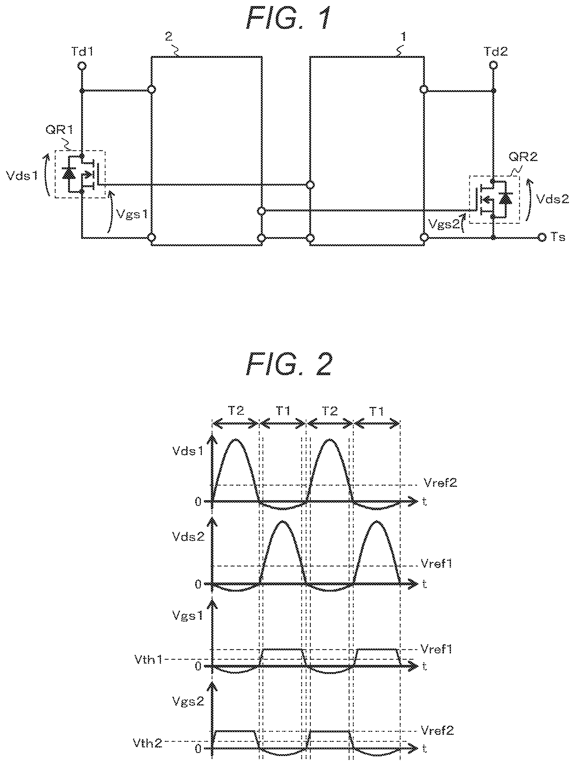
Hereinafter, embodiments of the present invention will be described with reference to the drawings. The same structures are denoted by the same reference numerals in the respective drawings and will not be described in detail redundantly. First Embodiment With reference to to 3 and to 14 , there will be described the structure of a rectifier circuit in a first embodiment of the present invention, and a method for controlling the rectifier circuit. is a view illustrating the structure of the rectifier circuit in the present embodiment, and is a diagram illustrating rectified waveforms created by the rectifier circuit in . is a view illustrating the structure of a rectification bridge to which the rectifier circuit of is applied. Incidentally, to 14 are views illustrating the structure of a conventional rectifier circuit and waveforms rectified which are thereby, illustrated as a comparative embodiment for facilitating understanding of the structure according to the present invention. First, the structure of the rectifier circuit in the present embodiment will be described with reference to . As illustrated in , the rectifier circuit in the present embodiment includes rectifying MOSFETs QR 1 and QR 2 (which may be simply referred to as QR 1 and QR 2 hereinafter), a control circuit 1 connected to a drain terminal and a source terminal of the rectifying MOSFET QR 2 and to a gate terminal and a source terminal of the rectifying MOSFET QR 1 , and a control circuit 2 connected to a drain terminal and a source terminal of the rectifying MOSFET QR 1 and to a gate terminal and a source terminal of the rectifying MOSFET QR 2 . Note that, in , the rectifying MOSFET QR 1 and the rectifying MOSFET QR 2 are represented as enhancement type N-channel MOSFETs, taking, as an example, a case of applying them as two rectifying MOSFETs LQ in the low-side of the rectification bridge in . The control circuit 1 receives a drain-source voltage Vds 2 of the rectifying MOSFET QR 2 as an input, and outputs a gate-source voltage Vgs 1 of the rectifying MOSFET QR 1 . Further, the control circuit 2 receives a drain-source voltage Vds 1 of the rectifying MOSFET QR 1 as an input, and outputs a gate-source voltage Vgs 2 of the rectifying MOSFET QR 2 . Next, operations of the rectifier circuit in the present embodiment will be described with reference to . illustrates voltage waveforms when the rectifier circuit of is applied as the two rectifying MOSFETs LQ in the low-side of the rectification bridge of and a sine wave voltage is applied thereto as an input voltage Vin. Time periods T 1 are rectification time periods for the rectifying MOSFET QR 1 , and are non-rectification time periods for the rectifying MOSFET QR 2 . Further, time periods T 2 are non-rectification time periods for the rectifying MOSFET QR 1 and are rectification time periods for the rectifying MOSFET QR 2 . In the rectification time periods T 1 for QR 1 , the control circuit 1 receives, as an input, the drain-source voltage Vds 2 applied to QR 2 , and outputs the gate-source voltage Vgs 1 of QR 1 . At this time, when the input voltage is smaller than a predetermined threshold voltage Vref 1 , the control circuit 1 outputs the input voltage as the output voltage, and when the input voltage is equal to or larger than the threshold voltage Vref 1 , the control circuit 1 clamps the output voltage at the threshold voltage Vref 1 . Further, in the rectification time periods T 2 for QR 2 , the control circuit 2 receives, as an input, the drain-source voltage Vds 1 applied to QR 1 , and outputs the gate-source voltage Vgs 2 of QR 2 . At this time, when the input voltage is smaller than a predetermined threshold voltage Vref 2 , the control circuit 2 outputs the input voltage as the output voltage, and when the input voltage is equal to or larger than the threshold voltage Vref 2 , the control circuit 2 clamps the output voltage at the threshold voltage Vref 2 . In this way, it is possible to prevent the gate-source voltages of QR 1 and QR 2 from becoming excessive. The threshold voltages Vref 1 and Vref 2 for the control circuits 1 and 2 are larger than gate threshold voltages Vth 1 and Vth 2 of QR 1 and QR 2 , respectively, in order to turn on QR 1 and QR 2 , Further, these threshold voltages Vref 1 and Vref 2 are smaller than maximum gate-source voltage ratings of QR 1 and QR 2 , respectively, in order to prevent failures of QR 1 and QR 2 . Further, the output voltage from the control circuit 1 is a voltage lower than a maximum value of the voltage between the drain and the source of the rectifying MOSFET QR 2 , and the output voltage from the control circuit 2 is a voltage lower than a maximum value of the voltage between the drain and the source of the rectifying MOSFET QR 1 . In this way, synchronous rectification is realized. Here, the aforementioned clamping refers to making the output voltage fall within a substantially constant range. For example, the clamping includes cases where the output voltage fluctuates due to noise mixed in the output voltage. Conventional Embodiment 1 Here, the structure of a conventional rectifier circuit will be described with reference to . The rectifier circuit of corresponds to the rectifier circuit in PTL 1 described above. The rectifier circuit of includes rectifying MOSFETs QR 1 and QR 2 , and control circuits CC 1 and CC 2 . Further, the control circuits CC 1 and CC 2 include drive circuits CC 12 and CC 22 , capacitors C 1 and C 2 , charging control circuits CC 13 and CC 23 , and MOSFETs CC 14 and CC 24 , respectively. Operations of the rectifier circuit of will be described with reference to . illustrates voltage waveforms when the rectifier circuit of is applied as the two rectifying MOSFETS LQ in the low-side of the rectification bridge of , and a sine wave voltage is applied thereto as the input voltage Vin. Time periods T 1 are rectification time periods for the rectifying MOSFET QR 1 , and are non-rectification time periods for the rectifying MOSFET QR 2 . Further, time periods T 2 are non-rectification time periods for the rectifying MOSFET QR 1 and are rectification time periods for the rectifying MOSFET QR 2 . As an example, attention is focused on operations of QR 1 . First, in a time period T 2 , in the control circuit CC 1 , the capacitor C 1 is charged by the input voltage Vin. By controlling the current for charging the capacitor C 1 through the MOSFET CC 14 , the voltage VC 1 across the capacitor C 1 is controlled to be a voltage with a predetermined magnitude. Next, in a time period T 1 , the voltage VC 1 across the capacitor C 1 is outputted as the gate-source voltage Vgs 1 of QR 1 . As described above, with the rectifier circuit illustrated in , it is necessary to accumulate the energy necessary for generating the gate-source voltages of the rectifying MOSFETs within the non-rectification time periods for the rectifying MOSFETs, which necessitates capacitors as energy accumulating elements. On the other hand, in the rectifier circuit in the present embodiment illustrated in , the energy necessary for generating a gate-source voltage of a rectifying MOSFET is obtained from the input voltage Vin, by using, as the input voltage to the control circuit, the drain-source voltage of another rectifying MOSFET which falls in the non-rectification time periods when the former rectifying MOSFET falls in the rectification time periods. This enables reduction of the capacitances of the capacitors as compared with those of the conventional rectifier circuit illustrated in . Conventional Embodiment 2 There will be described the structure of another conventional rectifier circuit, with reference to . The rectifier circuit of corresponds to the rectifier circuit in PTL 2 described above. The rectifier circuit of includes rectifying MOSFETs QR 1 and QR 2 , and voltage-dividing resistances Rp 1 to Rp 4 . Operations of the rectifier circuit of will be described with reference to . illustrates voltage waveforms when the rectifier circuit of is applied as the two rectifying MOSFETS LQ in the low-side of the rectification bridge of , and a sine wave voltage is applied thereto as the input voltage Vin. Time periods T 1 are rectification time periods for the rectifying MOSFET QR 1 , and are non-rectification time periods for the rectifying MOSFET QR 2 . Further, time periods T 2 are non-rectification time periods for the rectifying MOSFET QR 1 and are rectification time periods for the rectifying MOSFET QR 2 . As an example, attention is focused on operations of QR 1 . In the rectification time periods T 1 , the drain-source voltage Vds 2 of QR 2 is divided through the voltage dividing resistances Rp 1 and Rp 2 , and the voltage generated across Rp 2 is applied between the gate and the source of QR 1 . In , in the time periods T 1 , which are the rectification time periods for QR 1 , the waveform of the gate-source voltage Vgs 1 of QR 1 is a sine wave with an amplitude reduced by the voltage division by the resistances. As described above, with the rectifier circuit illustrated in , since the gate-source voltage of the rectifying MOSFET which is generated in the rectification time periods is a sine wave with an amplitude reduced by the voltage division by the resistances. This increases the time period from the start of a rectification time period until the gate-source voltage Vgs 1 , Vgs 2 gets larger than the gate threshold voltage Vth 1 , Vth 2 of the rectifying MOSFET QR 1 , QR 2 , and the time period from when the gate-source voltage Vgs 1 , Vgs 2 gets smaller than the gate threshold voltage Vth 1 , Vth 2 of the rectifying MOSFET QR 1 , QR 2 until the end of the rectification time period. Namely, the gate-source voltages Vgs 1 and Vgs 2 rise and fall slowly. This results in reduction of the proportion of the time period during which each rectifying MOSFET is on to a rectification time period, which deteriorates the loss reduction effect of synchronous rectification. On the other hand, in the rectifier circuit in the present embodiment illustrated in , when each input voltage is smaller than the threshold voltage Vref 1 , Vref 2 , the control circuit 1 , 2 outputs the input voltage as it is as the output voltage, without decreasing the input voltage through voltage division by resistances (in this case, voltage drops caused by resistance components of switches being in the ON states and resistance components of wirings in the control circuit are not regarded as being caused by voltage division through resistances). Namely, the gate-source voltages in the rectifier circuit of rise and fall more quickly than those in the rectifier circuit of . This results in an increase of the proportion of the time period during which each rectifying MOSFET is on to a rectification time period, which enhances the loss reduction effect of synchronous rectification. As described above, with the rectifier circuit in the present embodiment, it is possible to eliminate capacitors for supplying power for controlling the rectifying MOSFETs, while maintaining the loss reduction effect of synchronous rectification. Second Embodiment With reference to , there will be described the structure of a rectifier circuit in a second embodiment of the present invention, and a method for controlling the rectifier circuit. The present embodiment is an embodiment of a more specific circuit structure in the first embodiment. As illustrated in , the rectifier circuit in the present embodiment includes rectifying MOSFETs QR 1 and QR 2 , a control circuit 1 connected to a drain terminal and a source terminal of the rectifying MOSFET QR 2 and to a gate terminal and a source terminal of the rectifying MOSFET QR 1 , and a control circuit 2 connected to a drain terminal and a source terminal of the rectifying MOSFET QR 1 and to a gate terminal and a source terminal of the rectifying MOSFET QR 2 . The control circuit 1 includes a depression type N-channel MOSFET QS 1 having a drain terminal connected to the drain terminal of the rectifying MOSFET QR 2 and a source terminal connected to the gate terminal of the rectifying MOSFET QR 1 , a voltage-dividing resistance R 1 connected between the gate terminal and the source terminal of the N-channel MOSFET QS 1 , and a voltage-dividing resistance R 2 connected between the source terminal of the rectifying MOSFET QR 1 and the gate terminal of the N-channel MOSFET QS 1 . Further, the control circuit 2 includes a depression type N-channel MOSFET QS 2 having a drain terminal connected to the drain terminal of the rectifying MOSFET QR 1 and a source terminal connected to the gate terminal of the rectifying MOSFET QR 2 , a voltage-dividing resistance R 3 connected between the source terminal and the gate terminal of the N-channel MOSFET QS 2 , and a voltage-dividing resistance R 4 connected between the gate terminal of the N-channel MOSFET QS 2 and the source terminal of the rectifying MOSFET QR 2 . The rectifying MOSFETs QR 1 and QR 2 are N-channel MOSFETs having respective sources connected to a DC low-voltage terminal. The control circuit 1 and the control circuit 2 respectively include a MOSFET QS 1 for controlling an output voltage based on the drain-source voltage Vds 2 of the rectifying MOSFET QR 2 , which is the input voltage to the control circuit 1 , and a depression type N-channel MOSFET QS 1 , QS 2 as a switch for controlling an output voltage based on the drain-source voltage Vds 1 of the rectifying MOSFET QR 1 , which is the input voltage to the control circuit 2 . A method for determining the threshold voltages Vref 1 and Vref 2 will be described. As an example, a method for determining the threshold voltage Vref 1 will be described. Incidentally, it is assumed that the gate threshold voltage of the MOSFET QS 1 is Vth 11 , the on-resistance value of the MOSFET QS 1 is rqs1, and the resistance values of the resistance R 1 and the resistance R 2 are r1 and r2, respectively. When the input voltage to the control circuit 1 , namely the drain-source voltage Vds 2 of the rectifying MOSFET QR 2 is 0, the gate-source voltage of the MOSFET QS 1 is 0, and the MOSFET QS 1 is on since the MOSFET QS 1 is a depression type N-channel MOSFET. Thereafter, when Vds 2 is increased, the current flowing from the drain of the MOSFET QS 1 to the source thereof is increased. At this time, a voltage of Vds 2 ×(r1+r2)/(r1+r2+rqs1) is outputted as the output voltage from the control circuit 1 , as the gate-source voltage of the MOSFET QR 1 . Therefore, by selecting the MOSFET QS 1 and the resistances R 1 and R 2 such that the values of r1 and r1 are sufficiently larger than rqs1, it is possible to approximate the drain-source voltage Vds 2 of the rectifying MOSFET QR 2 , which is the input voltage to the control circuit 1 , and the gate-source voltage of the rectifying MOSFET QR 1 , which is the output voltage from the control circuit 1 , to the same value. When the drain-source voltage Vds 2 of the rectifying MOSFET QR 2 is increased, the current flowing from the drain of the MOSFET QS 1 to the source thereof is increased, but the voltage drop caused across the resistance R 1 is increased, which decreases the gate-source voltage of the MOSFET QS 1 (since it is a negative voltage, the absolute value thereof increases by an amount corresponding to the voltage drop caused across the resistance R 1 ), thereby increasing the on-resistance of QS 1 . As a result, when the drain-source voltage Vds 2 of the MOSFET QS 2 is equal to or larger than a certain voltage, the current flowing from the drain of the MOSFET QS 1 to the source thereof has a certain constant value. At this time, the voltage drop caused across the resistance R 1 and the voltage drop caused across the resistance R 2 are constant and, therefore, the gate-source voltage Vgs 1 of the rectifying MOSFET QR 1 is the sum of the voltage drop across the resistance R 1 and the voltage drop across the resistance R 2 , which is constant. The constant voltage at this time is the threshold voltage Vref 1 of the control circuit 1 . The threshold voltage Vref 1 can be approximated to Vth 11 ×(r1+r2)/r1. In order to obtain a desired threshold voltage Vref 1 , the gate threshold voltage Vth 11 of the MOSFET QS 1 and the resistance values r1 and r2 of the resistances R 1 and R 2 may be selected. The threshold voltage Vref 2 can be similarly determined. Third Embodiment With reference to , there will be described the structure of a rectifier circuit in a third embodiment of the present invention, and a method for controlling the rectifier circuit. As illustrated in , the rectifier circuit in the present embodiment includes enhancement type P-channel MOSFETs as rectifying MOSFETs QR 1 and QR 2 , and depression type P-channel MOSFETs as MOSFETs QS 1 and QS 2 . In the rectifier circuits in the first embodiment ( ) and the second embodiment ( ), the rectifying MOSFETs QR 1 and QR 2 are constituted by enhancement type N-channel MOSFETs, and QR 1 and QR 2 are provided with a common source terminal. Therefore, the rectifier circuits in cannot be applied as two rectifying MOSFETs HQ in the high-side, which are not provided with a common source terminal, in a rectification bridge constituted by four enhancement type N-channel MOSFETs as illustrated . For coping therewith, in the rectifier circuit in the present embodiment illustrated in , enhancement type P-channel MOSFETs are used as QR 1 and QR 2 , which enables providing QR 1 and QR 2 with a common source-side terminal even when they are applied as the two rectifying MOSFETS HQ in the high-side in . The rectifying MOSFETs QR 1 and QR 2 are constituted by P-channel MOSFETs having respective sources connected to a DC high-voltage terminal. Further, the MOSFETs QS 1 and QS 2 are constituted by depression type P-channel MOSFETs. With the structure of the rectifier circuit in the present embodiment, this rectifier circuit can be applied as a rectifier circuit in a high-side of a rectification bridge. Further, in the structure of the rectification bridge illustrated in , N-channel MOSFETs having respective sources connected to a DC low-voltage terminal may be used as the rectifying MOSFETs QR 1 and QR 2 in the DC low-voltage terminal side, while P-channel MOSFETs having respective sources connected to the DC high-voltage terminal may be used as the rectifying MOSFETs QR 1 and QR 2 in the DC high-voltage terminal side. Fourth Embodiment With reference to , there will be described the structure of a rectifier circuit in a fourth embodiment of the present invention, and a method for controlling the rectifier circuit. As illustrated in , in the rectifier circuit in the present embodiment, in addition to the structure in the second embodiment ( ), a control circuit 1 includes a comparator Co 1 and a gate driver GD 1 , and a control circuit 2 includes a comparator Co 2 and a gate driver GD 2 . Each of the rectifier circuits in the first embodiment ( ), the second embodiment ( ) and the third embodiment ( ) is assumed to be applied to a rectification bridge structured such that a resistive load is connected thereto in a subsequent stage. If each of these rectifier circuits is applied to a rectification bridge structured such that a capacitive load is connected thereto in a subsequent stage, a gate-source voltage of each rectifying MOSFET is generated in time periods other than the rectification time periods, which may cause short-circuiting between upper and lower arms. For coping therewith, as illustrated in , the rectifier circuit in the present embodiment is adapted to control the time periods during which gate-source voltages are generated, using the comparators Co 1 and Co 2 , and the gate drivers GD 1 and GD 2 . As an example, operations of the control circuit 1 will be described. As illustrated in , in the control circuit 1 , a source terminal of the MOSFET QS 2 and a source terminal of the rectifying MOSFET QR 1 are connected to differential input terminals of the comparator Co 1 , an output terminal of the comparator Co 1 is connected to an input terminal of the gate driver GD 1 , an output terminal of the gate driver is connected to a gate terminal of the rectifying MOSFET QR 1 , and a source terminal of the MOSFET QS 1 is connected to power supply terminals of the comparator Co 1 and the gate driver GD 1 . During the rectification time periods for the rectifying MOSFET QR 1 , the drain-source voltage of QR 1 has a negative value, due to the rectified current. At this time, the MOSFET QS 1 is on and, therefore, the comparator Co 1 detects a negative voltage and outputs an ON signal to the gate driver GD 1 , and the gate driver GD 1 outputs an output voltage clamped at the threshold voltage Vref 1 as the gate-source voltage Vgs 1 of the rectifying MOSFET QR 1 . In the aforementioned way, synchronous rectification can be realized. The same applies to the operation of the control circuit 2 . In the rectifier circuit of , the positive input terminals of the comparator Co 1 and the comparator Co 2 are connected to the source terminals of the rectifying MOSFETs QR 1 and QR 2 and, therefore, the determination voltage of the comparator Co 1 and the comparator Co 2 is 0 V. However, the determination voltage may be also made to be a negative voltage, in order to prevent short circuiting between the upper and lower arms, when the rectifier circuit is applied to a rectification bridge to which a capacitive load is connected. Furthermore, in order to suppress chattering, which rapidly turns on and off the rectifying MOSFETs QR 1 and QR 2 many times, the determination voltage may be provided with hysteresis. Further, as illustrated in , capacitors C 1 and C 2 may be used in the control circuit 1 and the control circuit 2 , respectively, in order to stabilize the power supply voltages for the comparators Co 1 and Co 2 and the gate drivers GD 1 and GD 2 . The capacitors C 1 and C 2 used in the rectifier circuit illustrated in are not required to hold energy during both on and off time periods for the rectifying MOSFETs QR 1 and QR 2 , unlike the capacitors C 1 and C 2 used in the conventional rectifier circuit illustrated in . This enables making the capacitances of the capacitors C 1 and C 2 in the present embodiment smaller than the capacitances of the capacitors C 1 and C 2 used in the conventional rectifier circuits of . With the rectifier circuit in the present embodiment, no gate-source voltage in the rectifying MOSFETs is generated in time periods other than the rectification time periods, which can advantageously avoid short circuiting between the upper and lower arms, in a rectification bridge structured such that a capacitive load is connected thereto in a subsequent stage. Fifth Embodiment A semiconductor package in a fifth embodiment of the present invention will be described with reference to . illustrates the rectifier circuit described in any one of the first to fourth embodiments, which is structured to be incorporated in a semiconductor package 4 . The semiconductor package 4 includes three terminals, which are a first terminal Td 1 , a second terminal Td 2 , and a third terminal Ts, as external terminals. illustrates the rectifier circuit described in the second embodiment ( ) as an example, while the rectifier circuits described in the other embodiments may be also used therein. There is an advantage of the present embodiment as follows. That is, in designing and fabricating a product using a rectifier circuit, by purchasing and introducing a rectifier circuit incorporating control circuits as that in the present embodiment, it is possible to eliminate the necessity of introducing control circuits themselves into designing and fabricating processes, which can reduce the number of processes required for designing and implementation. Sixth Embodiment There will be described a front-end power supply in a sixth embodiment of the present invention, with reference to . illustrates an example of a power supply to which the rectifier circuits according to the present invention described in the first to fifth embodiments can be applied. The present invention is applicable to an overall range of rectifier circuits used for power converters. For example, in the front-end power supply as illustrated in , the present invention can be applied thereto by being substituted for a rectifier circuit used at a position where commercial rectifying diodes CRD 1 to CRD 4 , freewheeling diodes FWD 1 and FWD 2 , and secondary rectifying diodes SSD 1 and SSD 2 are applied thereto. Also, the rectifier circuit in any one of the first, second, and fourth embodiments may be substituted for the commercial rectifying diodes CRD 3 and CRD 4 , and a synchronous rectifier circuit including diodes or power supply capacitors may be adopted as the commercial rectifying diodes CRD 1 and CRD 2 . By applying the rectifier circuit according to the present invention to a power supply such as a front-end power supply, it is possible to contribute to reduction of loss in the power supply and improvement of the reliability of the power supply. Incidentally, the present invention is not limited to the aforementioned embodiments, and covers various modifications. For example, the aforementioned embodiments have been described in detail, for the purpose of explaining the present invention in such a way as to facilitate understanding the present invention, and the present invention is not necessarily limited to structures including all the described structures. Further, the structure in a certain embodiment can be partially replaced with the structure in another embodiment and, also, the structure in a certain embodiment can be additionally provided with the structure in another embodiment. Further, the structure in each embodiment may be partially eliminated, provided with other additional structures or replaced with other structures. REFERENCE SIGNS LIST 1 , 2 control circuit 4 semiconductor package Td 1 , Td 2 , Ts terminal C 1 , C 2 capacitor R 1 , R 2 , R 3 , R 4 voltage dividing resistance LQ two rectifying MOSFETs in the low side of a rectification bridge HQ two rectifying MOSFETs in the high side of a rectification bridge CRD 1 to CRD 4 commercial rectifying diode FWD 1 , FWD 2 freewheeling diode SSD 1 , SSD 2 secondary rectifying diode QR 1 , QR 2 rectifying MOSFET QS 1 , QS 2 depression type N-channel MOSFET or depression type P-channel MOSFET Co 1 , Co 2 comparator GD 1 , GD 2 gate driver Vds 1 , Vds 2 the drain-source voltage of the rectifying MOSFET QR 1 , QR 2 Vgs 1 , Vgs 2 the gate-source voltage of the rectifying MOSFET QR 1 , QR 2 Vin input voltage Vth 1 , Vth 2 gate threshold voltage of the rectifying MOSFET QR 1 , QR 2 Vth 11 , Vth 22 gate threshold voltage of the MOSFET QS 1 , QS 2 Vref 1 , Vref 2 threshold voltage of the control circuit 1 , the control circuit 2 Vc 1 , Vc 2 voltage across the capacitor C 1 , C 2 T 1 , T 2 rectification time period for the rectifying MOSFET QR 1 , QR 2 Vgs 1 , Vgs 2 the gate-source voltage of the rectifying MOSFET QR 1 , QR 2 CC 1 , CC 2 control circuit in a conventional rectifier circuit Rp 1 to Rp 4 voltage dividing resistances in a conventional rectifier circuit
Figures (7)
Citations
This patent cites (20)
- US9729081
- US10756645
- US10784794
- US2010/0046259
- US2012/0218797
- US2012/0242390
- US2013/0077371
- US2014/0177305
- US2019/0044454
- US2020/0220477
- US2020/0287473
- US2021/0111640
- US108616269
- US111726011
- US2005-295627
- US2007020307
- US2009-142001
- US2021-520774
- USWO-2005124987
- USWO-2025164224