Abstract
A laminated coil component includes an element body including insulating layers laminated in a lamination direction, a coil inside the element body, and an external electrode on a surface of the element body and electrically connected to the coil. The coil includes a coil conductors laminated in the lamination direction and electrically connected via a via conductor penetrating the insulating layer in the lamination direction. The coil conductors include a first laminated portion including three or more of the coil conductors adjacent to each other, a second laminated portion including the coil conductors adjacent to each other such that a number of the coil conductors in the second laminated portion is the same as a number of the coil conductors in the first laminated portion, and an intermediate portion adjacent to and between the first and second laminated portions and including one or two of the coil conductors.
Claims (8)
1 . A laminated coil component comprising: an element body including a plurality of insulating layers laminated in a lamination direction; a coil inside the element body; and an external electrode on a surface of the element body and electrically connected to the coil, wherein the coil includes a plurality of coil conductors laminated in the lamination direction electrically connected via a via conductor penetrating the insulating layer in the lamination direction, the plurality of coil conductors laminated in the lamination direction includes a first laminated portion including three or more of the coil conductors adjacent to each other, a second laminated portion including the coil conductors adjacent to each other such that a number of the coil conductors in the second laminated portion is the same as a number of the coil conductors in the first laminated portion, and an intermediate portion between both of the laminated portions, and adjacent to both of the first laminated portion and the second laminated portion, and including one or two of the coil conductors, the first laminated portion has first parallel sections in which all the coil conductors constituting the first laminated portion overlap each other when viewed from the laminated direction, the first parallel sections are connected in parallel by the via conductor, the second laminated portion has second parallel sections in which all the coil conductors constituting the second laminated portion overlap each other when viewed from the laminated direction, the second parallel sections are connected in parallel by the via conductor, the first parallel sections and the second parallel sections overlap each other when viewed from the lamination direction, and all the coil conductors of the intermediate portion do not overlap each part of the first parallel sections and the second parallel sections when viewed from the laminated direction.
Show 7 dependent claims
2 . The laminated coil component according to claim 1 , wherein the intermediate portion includes one of the coil conductors.
3 . The laminated coil component according to claim 1 , wherein the lamination direction and a direction of a coil axis of the coil are along a same direction and are parallel to a mounting surface of the element body.
4 . The laminated coil component according to claim 1 , wherein a length of all the coil conductors of the first laminated portion, the second laminated portion, and the intermediate portion is a length of ¾ turns of the coil.
5 . The laminated coil component according to claim 2 , wherein the lamination direction and a direction of a coil axis of the coil are along a same direction and are parallel to a mounting surface of the element body.
6 . The laminated coil component according to claim 2 , wherein a length of all the coil conductors of the first laminated portion, the second laminated portion, and the intermediate portion is a length of ¾ turns of the coil.
7 . The laminated coil component according to claim 3 , wherein a length of all the coil conductors of the first laminated portion, the second laminated portion, and the intermediate portion is a length of ¾ turns of the coil.
8 . The laminated coil component according to claim 5 , wherein a length of all the coil conductors of the first laminated portion, the second laminated portion, and the intermediate portion is a length of ¾ turns of the coil.
Full Description
Show full text →
CROSS-REFERENCE TO RELATED APPLICATION
This application claims benefit of priority to Japanese Patent Application No. 2022-056389, filed Mar. 30, 2022, the entire content of which is incorporated herein by reference.
BACKGROUND
Technical Field The present disclosure relates to a laminated coil component. Background Art Japanese Patent Application Laid-Open No. 2019-9299 discloses a laminated inductor including a laminated body including a plurality of insulating layers laminated in a lamination direction, and a plurality of coil groups arranged in the laminated body along the lamination direction and connected in series, in which the coil group includes a plurality of coil patterns provided on the insulating layer and laminated in the lamination direction, and a plurality of pattern groups including n (n is a positive integer) coil patterns connected in parallel are connected in series. The parallel number n of at least one coil group is different from the parallel number n of other coil groups, a plurality of insulating layers include a magnetic insulating layer and a nonmagnetic insulating layer, and at least one of the insulating layers adjacent to the coil pattern is a nonmagnetic insulating layer.
SUMMARY
of Japanese Patent Application Laid-Open No. 2019-9299 discloses a laminated inductor configured by connecting, in series, a plurality of pattern groups formed by connecting three coil patterns in parallel. However, as a result of examination by the present inventors, it has been found that a problem below occurs in the laminated inductor illustrated in of Japanese Patent Application Laid-Open No. 2019-9299. In the laminated inductor illustrated in of Japanese Patent Application Laid-Open No. 2019-9299, in a combination of the pattern groups adjacent in a lamination direction, a region where the coil patterns do not overlap each other when viewed from the lamination direction exists for three layers in terms of insulating layers. For this reason, in the laminated inductor illustrated in of Japanese Patent Application Laid-Open No. 2019-9299, density is likely to locally lowered in the above region, and as a result, a problem that defects such as a crack are likely to occur in the laminated body is generated. Accordingly, the present disclosure provides a laminated coil component in which defects such as a crack are less likely to occur in an element body. A laminated coil component of the present disclosure includes an element body formed by a plurality of insulating layers laminated in a lamination direction, a coil provided inside the element body, and an external electrode provided on a surface of the element body and electrically connected to the coil. The coil includes a plurality of coil conductors laminated in the lamination direction electrically connected via a via conductor penetrating the insulating layer in the lamination direction. The plurality of the coil conductors laminated in the lamination direction includes a first laminated portion including three or more of the coil conductors adjacent to each other, a second laminated portion including the coil conductors adjacent to each other that are as many as the coil conductors in the first laminated portion (i.e., a number of the coil conductors in the second laminated portion is the same as the number of the coil conductors in the first laminated portion), and an intermediate portion adjacent to the first laminated portion and the second laminated portion between both of the laminated portions and including one or two of the coil conductors. The first laminated portion has a first parallel section in which all the coil conductors constituting the first laminated portion overlap each other when viewed from the laminated direction. The first parallel sections are connected in parallel by the via conductor. The second laminated portion has a second parallel section in which all the coil conductors constituting the second laminated portion overlap each other when viewed from the laminated direction. The second parallel sections are connected in parallel by the via conductor. The first parallel sections and the second parallel sections overlap each other when viewed from the lamination direction, and all the coil conductors constituting the intermediate portion do not overlap each part of the first parallel sections and the second parallel sections when viewed from the laminated direction. According to the present disclosure, it is possible to provide a laminated coil component in which defects such as a crack are less likely to occur in an element body.
BRIEF DESCRIPTION OF THE DRAWINGS
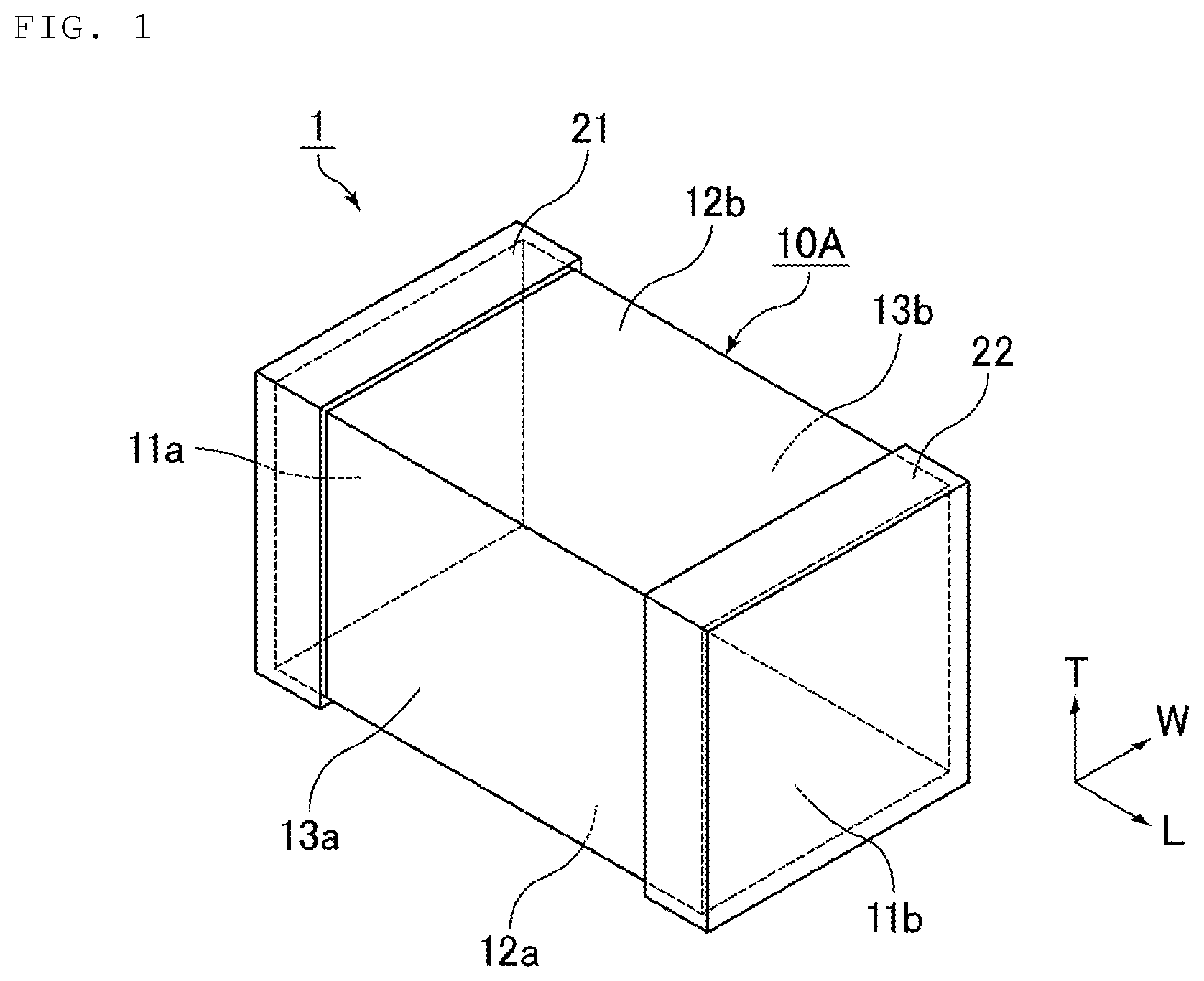
is a schematic perspective view illustrating an example of a laminated coil component according to a first embodiment of the present disclosure; is a schematic perspective view illustrating an example of a state in which the laminated coil component illustrated in (where an external electrode is excluded) is disassembled; is a schematic plan view illustrating an example of a state in which the laminated coil component illustrated in (where an external electrode is excluded) is disassembled; is an enlarged schematic sectional view illustrating an example of a state in which the vicinity of a first end surface of an element body is viewed in a sectional view from a height direction in the laminated coil component illustrated in ; is an enlarged schematic sectional view illustrating an example of a state in which the vicinity of a second end surface of the element body is viewed in a sectional view from the height direction in the laminated coil component illustrated in ; is a schematic plan view illustrating an example of a state in which the laminated coil component (where an external electrode is excluded) according to a second embodiment of the present disclosure is disassembled; is a schematic plan view illustrating an example of a state in which the laminated coil component (where an external electrode is excluded) according to the second embodiment of the present disclosure is disassembled, and illustrating a portion continuous with ; is a schematic plan view illustrating an example of a state in which the laminated coil component (where an external electrode is excluded) according to a third embodiment of the present disclosure is disassembled; is a schematic plan view illustrating an example of a state in which the laminated coil component (where an external electrode is excluded) according to the third embodiment of the present disclosure is disassembled, and illustrating a portion continuous with ; is a schematic plan view illustrating an example of a state in which the laminated coil component (where an external electrode is excluded) according to a fourth embodiment of the present disclosure is disassembled; and is a schematic plan view illustrating an example of a state in which the laminated coil component (where an external electrode is excluded) according to the fourth embodiment of the present disclosure is disassembled, and illustrating a portion continuous with .
DETAILED DESCRIPTION
Hereinafter, a laminated coil component of the present disclosure will be described. The present disclosure is not limited to a configuration below, and may be modified as appropriate without departing from the gist of the present disclosure. Further, a combination of a plurality of individual preferable configurations described below is also the present disclosure. It goes without saying that each of the embodiments illustrated below is an example, and partial replacement or combination of configurations illustrated in different embodiments is possible. In a second embodiment and subsequent embodiments, matters common to a first embodiment will not be described, and only a different point will be mainly described. In particular, the same operation and effect by the same configuration will not be sequentially mentioned for each embodiment. In description below, in a case where the embodiments are not particularly distinguished, they are simply referred to as the “laminated coil component of the present disclosure”. The drawings shown below are schematic views, and dimensions, scales of aspect ratios, and the like may be different from those of an actual product. A laminated coil component of the present disclosure includes an element body formed by a plurality of insulating layers laminated in a lamination direction, a coil provided inside the element body, and an external electrode provided on a surface of the element body and electrically connected to the coil. The coil includes a plurality of coil conductors laminated in the lamination direction electrically connected via a via conductor penetrating the insulating layer in the lamination direction. The plurality of the coil conductors laminated in the lamination direction includes a first laminated portion including three or more of the coil conductors adjacent to each other, a second laminated portion including the coil conductors adjacent to each other that are as many as the coil conductors in the first laminated portion (i.e., a number of the coil conductors in the second laminated portion is the same as the number of the coil conductors in the first laminated portion), and an intermediate portion adjacent to the first laminated portion and the second laminated portion between both of the laminated portions and including one or two of the coil conductors. The first laminated portion have a first parallel section in which all the coil conductors constituting the first laminated portion overlap each other when viewed from the laminated direction. The first parallel sections are connected in parallel by the via conductor. The second laminated portion have a second parallel section in which all the coil conductors constituting the second laminated portion overlap each other when viewed from the laminated direction. The second parallel sections are connected in parallel by the via conductor. The first parallel sections and the second parallel sections overlap each other when viewed from the lamination direction, and all the coil conductors constituting the intermediate portion do not overlap each part of the first parallel sections and the second parallel sections when viewed from the laminated direction. First Embodiment An example of the laminated coil component of the present disclosure will be described as the laminated coil component of the first embodiment of the present disclosure. In the laminated coil component according to the first embodiment of the present disclosure, each of a first laminated portion and a second laminated portion includes three coil conductors adjacent to each other. is a schematic perspective view illustrating an example of the laminated coil component according to the first embodiment of the present disclosure. A laminated coil component 1 illustrated in includes an element body 10 A, a first external electrode 21 , and a second external electrode 22 . Although not illustrated in , as described later, the laminated coil component 1 also includes a coil provided inside the element body 10 A. In the present description, a length direction, a height direction, and a width direction are respectively defined as L. T. and W, according to and the like. Here, the length direction L, the height direction T, and the width direction W are orthogonal to each other. The element body 10 A has a first end surface 11 a and a second end surface 11 b facing each other in the length direction L, a first main surface 12 a and a second main surface 12 b facing each other in the height direction T, and a first side surface 13 a and a second side surface 13 b facing each other in the width direction W, and has, for example, a rectangular parallelepiped shape or a substantially rectangular parallelepiped shape. The first end surface 11 a and the second end surface 11 b of the element body 10 A do not need to be strictly orthogonal to the length direction L. Further, the first main surface 12 a and the second main surface 12 b of the element body 10 A do not need to be strictly orthogonal to the height direction T. Furthermore, the first side surface 13 a and the second side surface 13 b of the element body 10 A do not need to be strictly orthogonal to the width direction W. In a case where the laminated coil component 1 is mounted on a substrate, the first main surface 12 a of the element body 10 A serves as a mounting surface. The element body 10 A preferably has a corner portion and a ridge portion that are rounded. The corner portion of the element body 10 A is a portion where three surfaces of the element body 10 A intersect. The ridge portion of the element body 10 A is a portion where two surfaces of the element body 10 A intersect. The first external electrode 21 is provided on a surface of the element body 10 A. More specifically, the first external electrode 21 extends from the first end surface 11 a of the element body 10 A over a part of each of the first main surface 12 a , the second main surface 12 b , the first side surface 13 a , and the second side surface 13 b. An arrangement mode of the first external electrode 21 is not limited to a mode illustrated in . For example, the first external electrode 21 may extend from a part of the first main surface 12 a of the element body 10 A to a part of each of the first end surface 11 a , the first side surface 13 a , and the second side surface 13 b. The second external electrode 22 is provided on a surface of the element body 10 A. More specifically, the second external electrode 22 extends from the second end surface 11 b of the element body 10 A over a part of each of the first main surface 12 a , the second main surface 12 b , the first side surface 13 a , and the second side surface 13 b. An arrangement mode of the second external electrode 22 is not limited to the mode illustrated in . For example, the second external electrode 22 may extend from a part of the first main surface 12 a of the element body 10 A to a part of each of the second end surface 11 b , the first side surface 13 a , and the second side surface 13 b. As described above, the first external electrode 21 and the second external electrode 22 are provided at positions separated from each other on a surface of the element body 10 A. As described above, since the first external electrode 21 and the second external electrode 22 are provided on the first main surface 12 a of the element body 10 A as a mounting surface, mountability of the laminated coil component 1 is improved. Each of the first external electrode 21 and the second external electrode 22 may have a single-layer structure or a multilayer structure. In a case where each of the first external electrode 21 and the second external electrode 22 has a single-layer structure, examples of a constituent material of each of the external electrodes include Ag, Au, Cu, Pd, Ni, Al, an alloy containing at least one of these types of metal, and the like. In a case where each of the first external electrode 21 and the second external electrode 22 has a multilayer structure, each of the external electrodes may have, for example, a base electrode containing Ag, a Ni plated electrode, and a Sn plated electrode in this order from the surface side of the element body 10 A. is a schematic perspective view illustrating an example of a state in which the laminated coil component illustrated in (where an external electrode is excluded) is disassembled. is a schematic plan view illustrating an example of a state in which the laminated coil component illustrated in (where an external electrode is excluded) is disassembled. As illustrated in , the element body 10 A includes a plurality of insulating layers laminated in a lamination direction, here, the length direction L. The element body 10 A includes an insulating layer P 1 , an insulating layer P 2 , an insulating layer P 3 , an insulating layer P 4 , an insulating layer P 5 , an insulating layer P 6 , an insulating layer P 7 , an insulating layer P 8 , an insulating layer P 9 , an insulating layer P 10 , an insulating layer P 11 , an insulating layer P 12 , an insulating layer P 13 , an insulating layer P 14 , and an insulating layer P 15 in order in the length direction L from the first end surface 11 a side toward the second end surface 11 b side. Examples of a constituent material of each insulating layer include a magnetic material such as a ferrite material. The ferrite material is preferably a Ni—Cu—Zn-based ferrite material. The Ni—Cu—Zn-based ferrite material preferably contains Fe in an amount of 40 mol % or more and 49.5 mol % or less (i.e., from 40 mol % to 49.5 mol %) in terms of Fe 2 O 3 , Zn in an amount of 2 mol % or more and 35 mol % or less (i.e., from 2 mol % to 35 mol %) in terms of ZnO, Cu in an amount of 6 mol % or more and 13 mol % or less (i.e., from 6 mol % to 13 mol %) in terms of CuO, and Ni in an amount of 10 mol % or more and 45 mol % or less (i.e. from 10 mol % to 45 mol %) in terms of NiO when the total amount is 100 mol %. The Ni—Cu—Zn-based ferrite material may further contain an additive such as Co, Bi, Sn, or Mn. The Ni—Cu—Zn-based ferrite material may further contain inevitable impurities. A coil 30 A is provided inside the element body 10 A. As illustrated in , the coil 30 A includes a coil conductor Q 1 , a coil conductor Q 2 , a coil conductor Q 3 , a coil conductor Q 4 , a coil conductor Q 5 , a coil conductor Q 6 , a coil conductor Q 7 , a coil conductor Q 8 , a coil conductor Q 9 , a coil conductor Q 10 , a coil conductor Q 11 , a coil conductor Q 12 , a coil conductor Q 13 , a coil conductor Q 14 , and a coil conductor Q 15 in order in the length direction L. The coil conductor Q 1 is linear and provided on a main surface of the insulating layer P 1 . The coil conductor Q 1 has a land portion Ra 1 and a land portion Rb 1 at different end portions. The coil conductor Q 2 has an L shape and is provided on a main surface of the insulating layer P 2 . The coil conductor Q 2 has a land portion Ra 2 and a land portion Rc 2 at different end portions. The land portion Ra 2 is connected to a via conductor Sa 2 penetrating the insulating layer P 2 in the length direction L. The via conductor Sa 2 is connected to the land portion Ra 1 in addition to the land portion Ra 2 . That is, the land portion Ra 1 and the land portion Ra 2 are electrically connected via the via conductor Sa 2 . The coil conductor Q 2 has a bent portion Ub 2 . The bent portion Ub 2 is connected to a via conductor Sb 2 penetrating the insulating layer P 2 in the length direction L. The via conductor Sb 2 is connected to the land portion Rb 1 in addition to the bent portion Ub 2 . That is, the land portion Rb 1 and the bent portion Ub 2 are electrically connected via the via conductor Sb 2 . The coil conductor Q 3 has a U shape and is provided on a main surface of the insulating layer P 3 . The coil conductor Q 3 has a land portion Ra 3 and a land portion Rd 3 at different end portions. The land portion Ra 3 is connected to a via conductor Sa 3 penetrating the insulating layer P 3 in the length direction L. The via conductor Sa 3 is connected to the land portion Ra 2 in addition to the land portion Ra 3 . That is, the land portion Ra 2 and the land portion Ra 3 are electrically connected via the via conductor Sa 3 . The coil conductor Q 3 has a bent portion Ub 3 and a bent portion Uc 3 . The bent portion Ub 3 is connected to the via conductor Sb 3 penetrating the insulating layer P 3 in the length direction L. The via conductor Sb 3 is connected to the bent portion Ub 2 in addition to the bent portion Ub 3 . That is, the bent portion Ub 2 and the bent portion Ub 3 are electrically connected via the via conductor Sb 3 . The bent portion Uc 3 is connected to a via conductor Sc 3 penetrating the insulating layer P 3 in the length direction L. The via conductor Sc 3 is connected to the land portion Rc 2 in addition to the bent portion Uc 3 . That is, the land portion Rc 2 and the bent portion Uc 3 are electrically connected via the via conductor Sc 3 . The coil conductor Q 4 has a U shape and is provided on a main surface of the insulating layer P 4 . The coil conductor Q 4 has a land portion Ra 4 and a land portion Rb 4 at different end portions. The land portion Rb 4 is connected to a via conductor Sb 4 penetrating the insulating layer P 4 in the length direction L. The via conductor Sb 4 is connected to the bent portion Ub 3 in addition to the land portion Rb 4 . That is, the bent portion Ub 3 and the land portion Rb 4 are electrically connected via the via conductor Sb 4 . The coil conductor Q 4 has a bent portion Uc 4 and a bent portion Ud 4 . The bent portion Uc 4 is connected to a via conductor Sc 4 penetrating the insulating layer P 4 in the length direction L. The via conductor Sc 4 is connected to the bent portion Uc 3 in addition to the bent portion Uc 4 . That is, the bent portion Uc 3 and the bent portion Uc 4 are electrically connected via the via conductor Sc 4 . The bent portion Ud 4 is connected to a via conductor Sd 4 penetrating the insulating layer P 4 in the length direction L. The via conductor Sd 4 is connected to the land portion Rd 3 in addition to the bent portion Ud 4 . That is, the land portion Rd 3 and the bent portion Ud 4 are electrically connected via the via conductor Sd 4 . The coil conductor Q 5 has a U shape and is provided on a main surface of the insulating layer P 5 . The coil conductor Q 5 has a land portion Rb 5 and a land portion Rc 5 at different end portions. The land portion Rc 5 is connected to a via conductor Sc 5 penetrating the insulating layer P 5 in the length direction L. The via conductor Sc 5 is connected to the bent portion Uc 4 in addition to the land portion Rc 5 . That is, the bent portion Uc 4 and the land portion Rc 5 are electrically connected via the via conductor Sc 5 . The coil conductor Q 5 has a bent portion Ua 5 and a bent portion Ud 5 . The bent portion Ua 5 is connected to a via conductor Sa 5 penetrating the insulating layer P 5 in the length direction L. The via conductor Sa 5 is connected to the land portion Ra 4 in addition to the bent portion Ua 5 . That is, the land portion Ra 4 and the bent portion Ua 5 are electrically connected via the via conductor Sa 5 . The bent portion Ud 5 is connected to a via conductor Sd 5 penetrating the insulating layer P 5 in the length direction L. The via conductor Sd 5 is connected to the bent portion Ud 4 in addition to the bent portion Ud 5 . That is, the bent portion Ud 4 and the bent portion Ud 5 are electrically connected via the via conductor Sd 5 . The coil conductor Q 6 has a U shape and is provided on a main surface of the insulating layer P 6 . The coil conductor Q 6 has a land portion Rc 6 and a land portion Rd 6 at different end portions. The land portion Rd 6 is connected to a via conductor Sd 6 penetrating the insulating layer P 6 in the length direction L. The via conductor Sd 6 is connected to the bent portion Ud 5 in addition to the land portion Rd 6 . That is, the bent portion Ud 5 and the land portion Rd 6 are electrically connected via the via conductor Sd 6 . The coil conductor Q 6 has a bent portion Ua 6 and a bent portion Ub 6 . The bent portion Ua 6 is connected to a via conductor Sa 6 penetrating the insulating layer P 6 in the length direction L. The via conductor Sa 6 is connected to the bent portion Ua 5 in addition to the bent portion Ua 6 . That is, the bent portion Ua 5 and the bent portion Ua 6 are electrically connected via the via conductor Sa 6 . The bent portion Ub 6 is connected to a via conductor Sb 6 penetrating the insulating layer P 6 in the length direction L. The via conductor Sb 6 is connected to the land portion Rb 5 in addition to the bent portion Ub 6 . That is, the land portion Rb 5 and the bent portion Ub 6 are electrically connected via the via conductor Sb 6 . The coil conductor Q 7 has a U shape and is provided on a main surface of the insulating layer P 7 . The coil conductor Q 7 has a land portion Ra 7 and a land portion Rd 7 at different end portions. The land portion Ra 7 is connected to a via conductor Sa 7 penetrating the insulating layer P 7 in the length direction L. The via conductor Sa 7 is connected to the bent portion Ua 6 in addition to the land portion Ra 7 . That is, the bent portion Ua 6 and the land portion Ra 7 are electrically connected via the via conductor Sa 7 . The coil conductor Q 7 has a bent portion Ub 7 and a bent portion Uc 7 . The bent portion Ub 7 is connected to a via conductor Sb 7 penetrating the insulating layer P 7 in the length direction L. The via conductor Sb 7 is connected to the bent portion Ub 6 in addition to the bent portion Ub 7 . That is, the bent portion Ub 6 and the bent portion Ub 7 are electrically connected via the via conductor Sb 7 . The bent portion Uc 7 is connected to a via conductor Sc 7 penetrating the insulating layer P 7 in the length direction L. The via conductor Sc 7 is connected to the land portion Rc 6 in addition to the bent portion Uc 7 . That is, the land portion Rc 6 and the bent portion Uc 7 are electrically connected via the via conductor Sc 7 . The coil conductor Q 8 has a U shape and is provided on a main surface of the insulating layer P 8 . The coil conductor Q 8 has a land portion Ra 8 and a land portion Rb 8 at different end portions. The land portion Rb 8 is connected to a via conductor Sb 8 penetrating the insulating layer P 8 in the length direction L. The via conductor Sb 8 is connected to the bent portion Ub 7 in addition to the land portion Rb 8 . That is, the bent portion Ub 7 and the land portion Rb 8 are electrically connected via the via conductor Sb 8 . The coil conductor Q 8 has a bent portion Uc 8 and a bent portion Ud 8 . The bent portion Uc 8 is connected to a via conductor Sc 8 penetrating the insulating layer P 8 in the length direction L. The via conductor Sc 8 is connected to the bent portion Uc 7 in addition to the bent portion Uc 8 . That is, the bent portion Uc 7 and the bent portion Uc 8 are electrically connected via the via conductor Sc 8 . The bent portion Ud 8 is connected to a via conductor Sd 8 penetrating the insulating layer P 8 in the length direction L. The via conductor Sd 8 is connected to the land portion Rd 7 in addition to the bent portion Ud 8 . That is, the land portion Rd 7 and the bent portion Ud 8 are electrically connected via the via conductor Sd 8 . The coil conductor Q 9 has a U shape and is provided on a main surface of the insulating layer P 9 . The coil conductor Q 9 has a land portion Rb 9 and a land portion Rc 9 at different end portions. The land portion Rc 9 is connected to a via conductor Sc 9 penetrating the insulating layer P 9 in the length direction L. The via conductor Sc 9 is connected to the bent portion Uc 8 in addition to the land portion Rc 9 . That is, the bent portion Uc 8 and the land portion Rc 9 are electrically connected via the via conductor Sc 9 . The coil conductor Q 9 has a bent portion Ua 9 and a bent portion Ud 9 . The bent portion Ua 9 is connected to a via conductor Sa 9 penetrating the insulating layer P 9 in the length direction L. The via conductor Sa 9 is connected to the land portion Ra 8 in addition to the bent portion Ua 9 . That is, the land portion Ra 8 and the bent portion Ua 9 are electrically connected via the via conductor Sa 9 . The bent portion Ud 9 is connected to a via conductor Sd 9 penetrating the insulating layer P 9 in the length direction L. The via conductor Sd 9 is connected to the bent portion Ud 8 in addition to the bent portion Ud 9 . That is, the bent portion Ud 8 and the bent portion Ud 9 are electrically connected via the via conductor Sd 9 . The coil conductor Q 10 has a U shape and is provided on a main surface of the insulating layer P 10 . The coil conductor Q 10 has a land portion Rc 10 and a land portion Rd 10 at different end portions. The land portion Rd 10 is connected to a via conductor Sd 10 penetrating the insulating layer P 10 in the length direction L. The via conductor Sd 10 is connected to the bent portion Ud 9 in addition to the land portion Rd 10 . That is, the bent portion Ud 9 and the land portion Rd 10 are electrically connected via the via conductor Sd 10 . The coil conductor Q 10 has a bent portion Ua 10 and a bent portion Ub 10 . The bent portion Ua 10 is connected to a via conductor Sa 10 penetrating the insulating layer P 10 in the length direction L. The via conductor Sa 10 is connected to the bent portion Ua 9 in addition to the bent portion Ua 10 . That is, the bent portion Ua 9 and the bent portion Ua 10 are electrically connected via the via conductor Sa 10 . The bent portion Ub 10 is connected to a via conductor Sb 10 penetrating the insulating layer P 10 in the length direction L. The via conductor Sb 10 is connected to the land portion Rb 9 in addition to the bent portion Ub 10 . That is, the land portion Rb 9 and the bent portion Ub 10 are electrically connected via the via conductor Sb 10 . The coil conductor Q 11 has a U shape and is provided on a main surface of the insulating layer P 11 . The coil conductor Q 11 has a land portion Ra 11 and a land portion Rd 11 at different end portions. The land portion Ra 11 is connected to a via conductor Sa 11 penetrating the insulating layer P 11 in the length direction L. The via conductor Sa 11 is connected to the bent portion Ua 10 in addition to the land portion Ra 11 . That is, the bent portion Ua 10 and the land portion Ra 11 are electrically connected via the via conductor Sa 11 . The coil conductor Q 11 has a bent portion Ub 11 and a bent portion Uc 11 . The bent portion Ub 11 is connected to a via conductor Sb 11 penetrating the insulating layer P 11 in the length direction L. The via conductor Sb 11 is connected to the bent portion Ub 10 in addition to the bent portion Ub 11 . That is, the bent portion Ub 10 and the bent portion Ub 11 are electrically connected via the via conductor Sb 11 . The bent portion Uc 11 is connected to a via conductor Sc 11 penetrating the insulating layer P 11 in the length direction L. The via conductor Sc 11 is connected to the land portion Rc 10 in addition to the bent portion Uc 11 . That is, the land portion Rc 10 and the bent portion Uc 11 are electrically connected via the via conductor Sc 11 . The coil conductor Q 12 has a U shape and is provided on a main surface of the insulating layer P 12 . The coil conductor Q 12 has a land portion Ra 12 and a land portion Rb 12 at different end portions. The land portion Rb 12 is connected to a via conductor Sb 12 penetrating the insulating layer P 12 in the length direction L. The via conductor Sb 12 is connected to the bent portion Ub 11 in addition to the land portion Rb 12 . That is, the bent portion Ub 11 and the land portion Rb 12 are electrically connected via the via conductor Sb 12 . The coil conductor Q 12 has a bent portion Uc 12 and a bent portion Ud 12 . The bent portion Uc 12 is connected to a via conductor Sc 12 penetrating the insulating layer P 12 in the length direction L. The via conductor Sc 12 is connected to the bent portion Uc 11 in addition to the bent portion Uc 12 . That is, the bent portion Uc 11 and the bent portion Uc 12 are electrically connected via the via conductor Sc 12 . The bent portion Ud 12 is connected to a via conductor Sd 12 penetrating the insulating layer P 12 in the length direction L. The via conductor Sd 12 is connected to the land portion Rd 11 in addition to the bent portion Ud 12 . That is, the land portion Rd 11 and the bent portion Ud 12 are electrically connected via the via conductor Sd 12 . The coil conductor Q 13 has a U shape and is provided on a main surface of the insulating layer P 13 . The coil conductor Q 13 has a land portion Rb 13 and a land portion Rc 13 at different end portions. The land portion Rc 13 is connected to a via conductor Sc 13 penetrating the insulating layer P 13 in the length direction L. The via conductor Sc 13 is connected to the bent portion Uc 12 in addition to the land portion Rc 13 . That is, the bent portion Uc 12 and the land portion Rc 13 are electrically connected via the via conductor Sc 13 . The coil conductor Q 13 has a bent portion Ua 13 and a bent portion Ud 13 . The bent portion Ua 13 is connected to a via conductor Sa 13 penetrating the insulating layer P 13 in the length direction L. The via conductor Sa 13 is connected to the land portion Ra 12 in addition to the bent portion Ua 13 . That is, the land portion Ra 12 and the bent portion Ua 13 are electrically connected via the via conductor Sa 13 . The bent portion Ud 13 is connected to a via conductor Sd 13 penetrating the insulating layer P 13 in the length direction L. The via conductor Sd 13 is connected to the bent portion Ud 12 in addition to the bent portion Ud 13 . That is, the bent portion Ud 12 and the bent portion Ud 13 are electrically connected via the via conductor Sd 13 . The coil conductor Q 14 has an L shape and is provided on a main surface of the insulating layer P 14 . The coil conductor Q 14 has a land portion Rb 14 and a land portion Rd 14 at different end portions. The land portion Rb 14 is connected to a via conductor Sb 14 penetrating the insulating layer P 14 in the length direction L. The via conductor Sb 14 is connected to the land portion Rb 13 in addition to the land portion Rb 14 . That is, the land portion Rb 13 and the land portion Rb 14 are electrically connected via the via conductor Sb 14 . The land portion Rd 14 is connected to a via conductor Sd 14 penetrating the insulating layer P 14 in the length direction L. The via conductor Sd 14 is connected to the bent portion Ud 13 in addition to the land portion Rd 14 . That is, the bent portion Ud 13 and the land portion Rd 14 are electrically connected via the via conductor Sd 14 . The coil conductor Q 14 has a bent portion Ua 14 . The bent portion Ua 14 is connected to a via conductor Sa 14 penetrating the insulating layer P 14 in the length direction L. The via conductor Sa 14 is connected to the bent portion Ua 13 in addition to the bent portion Ua 14 . That is, the bent portion Ua 13 and the bent portion Ua 14 are electrically connected via the via conductor Sa 14 . The coil conductor Q 15 has a linear shape and is provided on a main surface of the insulating layer P 15 . The coil conductor Q 15 has a land portion Ra 15 and a land portion Rb 15 at different end portions. The land portion Ra 15 is connected to a via conductor Sa 15 penetrating the insulating layer P 15 in the length direction L. The via conductor Sa 15 is connected to the bent portion Ua 14 in addition to the land portion Ra 15 . That is, the bent portion Ua 14 and the land portion Ra 15 are electrically connected via the via conductor Sa 15 . The land portion Rb 15 is connected to a via conductor Sb 15 penetrating the insulating layer P 15 in the length direction L. The via conductor Sb 15 is connected to the land portion Rb 14 in addition to the land portion Rb 15 . That is, the land portion Rb 14 and the land portion Rb 15 are electrically connected via the via conductor Sb 15 . In the present description, the L shape only needs to be a shape in which two sides are substantially orthogonal to each other, and does not need to be a shape in which two sides are strictly orthogonal to each other. In the present description, the U shape only needs to be a shape in which two adjacent sides of three sides are substantially orthogonal to each other, and does not need to be a shape in which two adjacent sides of three sides are strictly orthogonal to each other. In the laminated coil component 1 , as described above, the insulating layer P 1 , the insulating layer P 2 , the insulating layer P 3 , the insulating layer P 4 , the insulating layer P 5 , the insulating layer P 6 , the insulating layer P 7 , the insulating layer P 8 , the insulating layer P 9 , the insulating layer P 10 , the insulating layer P 11 , the insulating layer P 12 , the insulating layer P 13 , the insulating layer P 14 , and the insulating layer P 15 are laminated in order in the length direction L. By the above, the coil conductor Q 1 , the coil conductor Q 2 , the coil conductor Q 3 , the coil conductor Q 4 , the coil conductor Q 5 , the coil conductor Q 6 , the coil conductor Q 7 , the coil conductor Q 8 , the coil conductor Q 9 , the coil conductor Q 10 , the coil conductor Q 11 , the coil conductor Q 12 , the coil conductor Q 13 , the coil conductor Q 14 , and the coil conductor Q 15 are electrically connected via the via conductors described above while being laminated in order in the length direction L together with the insulating layer, and as a result, the coil 30 A is configured. The coil 30 A has, for example, a solenoid shape. When viewed from the length direction L, the coil 30 A may have a shape constituted by a straight portion (for example, a polygonal shape) as illustrated in , a shape constituted by a curved portion (for example, a circular shape), or a shape constituted by a straight portion and a curved portion. In the laminated coil component of the present disclosure, the lamination direction and a direction of a coil axis of the coil are preferably parallel to a mounting surface of the element body along the same direction. In the element body 10 A, the lamination direction of the insulating layer is parallel to the length direction L. That is, the lamination direction of the insulating layer is parallel to the first main surface 12 a of the element body 10 A which is a mounting surface. The coil 30 A has a coil axis C. The coil axis C of the coil 30 A corresponds to a central axis of the coil 30 A when viewed from the length direction L, and extends in the length direction L. That is, a direction of the coil axis C of the coil 30 A is parallel to the first main surface 12 a of the element body 10 A which is a mounting surface. Therefore, in the laminated coil component 1 , the lamination direction of the insulating layer and the direction of the coil axis C of the coil 30 A are parallel to the first main surface 12 a of the element body 10 A as a mounting surface along the same length direction L. In the laminated coil component 1 , a mode in which the lamination direction of the insulating layer and the direction of the coil axis C of the coil 30 A are parallel to the first main surface 12 a of the element body 10 A as a mounting surface along the same length direction L. However, the lamination direction of the insulating layer and the direction of the coil axis of the coil may be orthogonal to the first main surface of the element body as a mounting surface. In the laminated coil component 1 , a plurality of coil conductors laminated in the length direction L include a first laminated portion Ea 1 , a second laminated portion Fa 1 , and an intermediate portion Ga 1 . The first laminated portion Ea 1 includes three of the coil conductors Q 3 , Q 4 , and Q 5 adjacent to each other. The first laminated portion Ea 1 has a first parallel section Ma 1 in which all the coil conductors constituting the first laminated portion Ea 1 , that is, the coil conductor Q 3 , the coil conductor Q 4 , and the coil conductor Q 5 overlap each other when viewed from the length direction L. The first parallel sections Ma 1 are connected in parallel by the via conductor Sc 4 , the via conductor Sd 4 , the via conductor Sc 5 , and the via conductor Sd 5 . That is, the coil conductor Q 3 , the coil conductor Q 4 , and the coil conductor Q 5 are connected in parallel in the first parallel sections Ma 1 . All of the coil conductor Q 3 , the coil conductor Q 4 , and the coil conductor Q 5 do not overlap each other when viewed from the length direction L in a section other than the first parallel section Ma 1 . The second laminated portion Fa 1 includes three of the coil conductors Q 7 , Q 8 , and Q 9 adjacent to each other which are as many as the coil conductors in the first laminated portion Ea 1 (i.e., a number of the coil conductors Q 7 , Q 8 and Q 9 in the second laminated portion Fa 1 is the same as the number of the coil conductors Q 3 , Q 4 and Q 5 in the first laminated portion Ea 1 ). The second laminated portion Fa 1 has a second parallel section Na 1 in which all the coil conductors constituting the second laminated portion Fa 1 , that is, the coil conductor Q 7 , the coil conductor Q 8 , and the coil conductor Q 9 overlap each other when viewed from the length direction L. The second parallel sections Na 1 are connected in parallel by the via conductor Sc 8 , the via conductor Sd 8 , the via conductor Sc 9 , and the via conductor Sd 9 . That is, the coil conductor Q 7 , the coil conductor Q 8 , and the coil conductor Q 9 are connected in parallel in the second parallel sections Na 1 . All of the coil conductor Q 7 , the coil conductor Q 8 , and the coil conductor Q 9 do not overlap each other when viewed from the length direction L in a section other than the second parallel section Na 1 . The first parallel section Ma 1 and the second parallel section Na 1 overlap each other when viewed from the length direction L. In the above description, in the laminated coil component 1 , the first laminated portion Ea 1 and the second laminated portion Fa 1 are exemplified as laminated portions including three coil conductors adjacent to each other, but the same applies to laminated portions including another combination of three coil conductors adjacent to each other. That is, in the laminated coil component 1 , three coil conductors adjacent to each other are connected in parallel in a parallel section in which the coil conductors overlap each other when viewed from the length direction L. In the laminated coil component 1 , since three coil conductors adjacent to each other are connected in parallel in a parallel section, a sectional area of the coil 30 A orthogonal to a direction along a current path of the coil 30 A, that is, a direction in which the coil conductor extends increases accordingly. Therefore, in the laminated coil component 1 , direct current resistance (Rdc) of the coil 30 A becomes low, and large current can flow through the coil 30 A. The intermediate portion Ga 1 is adjacent to the first laminated portion Ea 1 and the second laminated portion Fa 1 between both of the laminated portions, and includes one of the coil conductor Q 6 . All the coil conductors constituting the intermediate portion Ga 1 , that is, the coil conductor Q 6 does not overlap each part of the first parallel section Ma 1 and the second parallel section Na 1 when viewed from the length direction L. More specifically, the coil conductor Q 6 does not overlap a region (region surrounded by a broken line) other than both ends (including a connection portion where a coil conductor and a via conductor are connected) of the first parallel section Ma 1 and a region (region surrounded by a broken line) other than both ends (including a connection portion where a coil conductor and a via conductor are connected) of the second parallel section Na 1 when viewed from the length direction L. Therefore, in the laminated coil component 1 , when viewed from the length direction L, between the first parallel section Ma 1 and the second parallel section Na 1 , a region where no coil conductor is present exists only for one layer in terms of an insulating layer. In the above description, in the laminated coil component 1 , a combination of the first laminated portion Ea 1 , the second laminated portion Fa 1 , and the intermediate portion Ga 1 is described, but the same applies to another combination. That is, in the laminated coil component 1 , when viewed from the length direction L, a region where no coil conductor is present exists only for one layer in terms of an insulating layer between the first parallel section and the second parallel section. Therefore, in the laminated coil component 1 , for example, density is less likely to be locally lowered as compared with the laminated inductor illustrated in of Japanese Patent Application Laid-Open No. 2019-9299. Therefore, in the laminated coil component 1 , for example, defects such as a crack are less likely to occur in the element body 10 A as compared with the laminated inductor illustrated in of Japanese Patent Application Laid-Open No. 2019-9299. In the laminated coil component of the present disclosure, the intermediate portion preferably includes one of the coil conductors. In the laminated coil component 1 , for example, the intermediate portion Ga 1 includes one of the coil conductor Q 6 . That is, in the laminated coil component 1 , when viewed from the length direction L, between the first parallel section Ma 1 and the second parallel section Na 1 , a region where no coil conductor is present exists only for one layer in terms of an insulating layer. By the above, in the laminated coil component 1 , local decrease in density is sufficiently prevented. In the laminated coil component of the present disclosure, a length of all the coil conductors constituting the first laminated portion, the second laminated portion, and the intermediate portion may be a length of ¾ turns of the coil. In the laminated coil component 1 , for example, a length of all the coil conductors constituting the first laminated portion Ea 1 , the second laminated portion Fa 1 , and the intermediate portion Ga 1 is a length of ¾ turns of the coil 30 A. In the present description, a length of the coil conductor means a length in a direction in which the coil conductor extends on a plane orthogonal to the lamination direction when viewed from the lamination direction (the length direction L in ). The element body 10 A further includes an insulating layer Px. The insulating layer Px is laminated on the first end surface 11 a side of the insulating layer P 1 , that is, on the side of the insulating layer P 1 opposite to the insulating layer P 2 . On a main surface of the insulating layer Px, a lead-out land portion Rax is provided. The lead-out land portion Rax is connected to a lead-out via conductor Sax penetrating the insulating layer Px in the length direction L. In addition to the lead-out via conductor Sax, the lead-out land portion Rax is also connected to a lead-out via conductor Sa 1 penetrating the insulating layer P 1 in the length direction L. By the above, a first lead-out conductor 41 including the lead-out land portion Rax, the lead-out via conductor Sax, and the lead-out via conductor Sa 1 is configured. The lead-out via conductor Sa 1 is connected to the land portion Ra 1 in addition to the lead-out land portion Rax. That is, the first lead-out conductor 41 is connected to the coil 30 A. is an enlarged schematic sectional view illustrating an example of a state in which the vicinity of a first end surface of an element body is viewed in a sectional view from the height direction in the laminated coil component illustrated in . As illustrated in , since the insulating layer Px is laminated on the insulating layer P 1 on the side opposite to the insulating layer P 2 , the first lead-out conductor 41 is exposed from the first end surface 11 a of the element body 10 A. The exposed portion of the first lead-out conductor 41 is connected to the first external electrode 21 provided on the first end surface 11 a of the element body 10 A. Therefore, the coil 30 A and the first external electrode 21 are electrically connected via the first lead-out conductor 41 . Note that, in , boundaries between the insulating layers are illustrated for convenience of description, but these boundaries do not clearly appear in practice. The number of the insulating layers Px may be one or more. In a case where the number of the insulating layers Px is plural, the first lead-out conductor 41 is formed by a plurality of the lead-out land portions Rax and a plurality of the lead-out via conductors Sax connected to each other and the lead-out via conductor Sa 1 that is further connected. The element body 10 A further includes an insulating layer Py. The insulating layer Py is laminated on the second end surface 11 b side of the insulating layer P 15 , that is, on the side of the insulating layer P 15 opposite to the insulating layer P 14 . On a main surface of the insulating layer Py, a lead-out land portion Rby is provided. The lead-out land portion Rby is connected to a lead-out via conductor Sby penetrating the insulating layers Py in the length direction L. By the above, a second lead-out conductor 42 including the lead-out land portion Rby and the lead-out via conductor Sby is configured. The lead-out via conductor Sby is connected to the land portion Rb 15 in addition to the lead-out land portion Rby. That is, the second lead-out conductor 42 is connected to the coil 30 A. is an enlarged schematic sectional view illustrating an example of a state in which the vicinity of a second end surface of the element body is viewed in a sectional view from the height direction in the laminated coil component illustrated in . As illustrated in , since the insulating layer Py is laminated on the insulating layer P 15 on the side opposite to the insulating layer P 14 , the second lead-out conductor 42 is exposed from the second end surface 11 b of the element body 10 A. The exposed portion of the second lead-out conductor 42 is connected to the second external electrode 22 provided on the second end surface 11 b of the element body 10 A. Therefore, the coil 30 A and the second external electrode 22 are electrically connected via the second lead-out conductor 42 . Note that, in , boundaries between the insulating layers are illustrated for convenience of description, but these boundaries do not clearly appear in practice. The number of the insulating layers Py may be one or more. In a case where the number of the insulating layers Py is plural, the second lead-out conductor 42 is formed by a plurality of the lead-out land portions Rby and a plurality of the lead-out via conductors Sby connected to each other. The numbers of the insulating layers Px and Py may be the same or different from each other. The laminated coil component 1 does not need to have at least one of the first lead-out conductor 41 and the second lead-out conductor 42 . Examples of a constituent material of each coil conductor (including a land portion), each via conductor, and each lead-out via conductor include Ag, Au, Cu, Pd, Ni, Al, and an alloy containing at least one type of the metal. When viewed from the length direction L, each coil conductor may have a shape constituted by a straight portion as illustrated in , a shape constituted by a curved portion, or a shape constituted by a straight portion and a curved portion. When viewed from the length direction L, each land portion may have a circular shape or a polygonal shape. When viewed from the length direction L, each via conductor may have a circular shape or a polygonal shape. When viewed from the length direction L, each lead-out via conductor may have a circular shape or a polygonal shape. Each coil conductor and each lead-out conductor may not independently have a land portion. The laminated coil component 1 is manufactured, for example, by a method below. <Producing Process of Magnetic Material> First, Fe 2 O 3 , ZnO, CuO, and NiO are weighed so as to have a predetermined ratio. Next, these weighed materials, pure water, and the like are put in a ball mill together with PSZ media, mixed, and then pulverized. Mixing and pulverizing time is, for example, four hours or more and eight hours or less (i.e., from four hours to eight hours). Then, the obtained pulverized material is dried and then pre-fired. The pre-firing temperature is, for example, 700° C. or more and 800° C. or less (i.e., from 700° C. to 800° C.). The pre-firing time is, for example, two hours or more and five hours or less (i.e., from two hours to five hours). In this way, a powdery magnetic material, more specifically, a powdery magnetic ferrite material is produced. The ferrite material is preferably a Ni—Cu—Zn-based ferrite material. The Ni—Cu—Zn-based ferrite material preferably contains Fe in an amount of 40 mol % or more and 49.5 mol % or less (i.e., from 40 mol % to 49.5 mol %) in terms of Fe 2 O 3 , Zn in an amount of 2 mol % or more and 35 mol % or less (i.e., from 2 mol % to 35 mol %) in terms of ZnO, Cu in an amount of 6 mol % or more and 13 mol % or less (i.e., from 6 mol % to 13 mol %) in terms of CuO, and Ni in an amount of 10 mol % or more and 45 mol % or less (i.e., from 10 mol % to 45 mol %) in terms of NiO when the total amount is 100 mol %. The Ni—Cu—Zn-based ferrite material may further contain an additive such as Co, Bi, Sn, or Mn. The Ni—Cu—Zn-based ferrite material may further contain inevitable impurities. <Producing Process of Green Sheet> First, a magnetic material, an organic binder such as polyvinyl butyral-based resin, an organic solvent such as ethanol or toluene, a plasticizer, and the like are put in a ball mill together with PSZ media and mixed, and then pulverized to produce slurry. Next, the slurry is formed into a sheet shape having a predetermined thickness by a doctor blade method or the like, and then punched into a predetermined shape to produce a green sheet. The thickness of the green sheet is, for example, 20 μm or more and 30 μm or less (i.e., from 20 μm to 30 μm). The shape of the green sheet is, for example, a rectangular shape. As a material of the green sheet, a nonmagnetic material such as a borosilicate glass material may be used instead of the magnetic material, or a mixed material of the magnetic material and the nonmagnetic material may be used. <Formation Process of Conductor Pattern> First, a predetermined portion of the green sheet is irradiated with a laser to form a via hole. Next, conductive paste such as Ag paste is applied to a surface of the green sheet while the via hole is filled with the conductive paste by a screen printing method or the like. By the above, a conductor pattern for a coil conductor connected to a conductor pattern for a via conductor is formed on a surface of the green sheet while the conductor pattern for a via conductor is formed in the via hole. In this way, a coil sheet in which the conductor pattern for a coil conductor and the conductor pattern for a via conductor are formed on the green sheet is produced. A plurality of coil sheets are prepared, and a conductor pattern for a coil conductor corresponding to the coil conductor illustrated in and a conductor pattern for a via conductor corresponding to a via conductor (including the lead-out via conductor Sa 1 illustrated in ) connected to the coil conductor illustrated in are formed for each coil sheet. Further, conductive paste such as Ag paste is applied to a surface of the green sheet while the via hole is filled with the conductive paste by a screen printing method or the like. By the above, a conductor pattern for a land portion connected to a conductor pattern for a via conductor is formed on a surface of the green sheet while the conductor pattern for a via conductor is formed in the via hole. In this way, a via sheet in which the conductor pattern for a land portion and the conductor pattern for a via conductor are formed on the green sheet is produced separately from a coil sheet. A plurality of the via sheets are also prepared, and a conductor pattern for a land portion corresponding to the lead-out land portion constituting the lead-out conductor illustrated in and a conductor pattern for a via conductor corresponding to the lead-out via conductor (excluding the lead-out via conductor Sa 1 illustrated in ) connected to the lead-out land portion illustrated in are formed on each of the via sheets. <Producing Process of Laminate Block> The coil sheet and the via sheet are laminated in the lamination direction (the length direction L in ) in the order corresponding to , and then thermocompression-bonded to produce a laminate block. <Producing Process of Element Body and Coil> First, the laminated body block is cut into predetermined size with a dicer or the like to produce a chip as an individual piece. Next, the chip as an individual piece is fired. The firing temperature is, for example, 900° C. or more and 920° C. or less (i.e., from 900° C. to 920° C.). The firing time is, for example, two hours or more and four hours or less (i.e., from two hours to four hours). When the chip as an individual piece is fired, the green sheets of the coil sheet and the via sheet become insulating layers. As a result, an element body formed of a plurality of the insulating layers laminated in the lamination direction (the length direction L in ) is produced. When the chip as an individual piece is fired, the conductor pattern for a coil conductor and the conductor pattern for a via conductor of the coil sheet become a coil conductor and a via conductor (including the lead-out via conductor Sa 1 illustrated in ), respectively. As a result, a coil in which a plurality of the coil conductors laminated in the lamination direction (the length direction L in ) are electrically connected via the via conductor is produced. As described above, the element body and the coil provided inside the element body are produced. On the other hand, when the chip as an individual piece is fired, the conductor pattern for a land portion and the via conductor pattern of the via sheet become the lead-out land portion and the lead-out via conductor, respectively. As a result, the first lead-out conductor and the second lead-out conductor formed of a plurality of lead-out land portions and a plurality of lead-out via conductors laminated in the lamination direction (the length direction L in ) and connected alternately are produced. The first lead-out conductor is exposed from the first end surface of the element body. The second lead-out conductor is exposed from the second end surface of the element body. The element body may be subjected to, for example, barrel polishing so that a corner portion and a ridge portion are rounded. <Forming Process of External Electrode> First, by applying conductive paste such as paste containing Ag and glass frit, a first coating film connected to the first lead-out conductor exposed from the first end surface of the element body is formed so as to extend from the first end surface of the element body over a part of each of the first main surface, the second main surface, the first side surface, and the second side surface. Further, by applying conductive paste such as paste containing Ag and glass frit, a second coating film connected to the second lead-out conductor exposed from the second end surface of the element body is formed so as to extend from the second end surface of the element body over a part of each of the first main surface, the second main surface, the first side surface, and the second side surface. In this way, the first coating film and the second coating film are formed at positions separated from each other on a surface of the element body. When the first coating film and the second coating film are formed, the first coating film and the second coating film may be formed at different timings, or may be formed at the same timing. In a case where the first coating film and the second coating film are formed at different timings, the first coating film and the second coating film may be formed in this order, or the second coating film and the first coating film may be formed in this order. Next, by baking the first coating film, a first base electrode extending from the first end surface of the element body over a part of each of the first main surface, the second main surface, the first side surface, and the second side surface and connected to the first lead-out conductor is formed. Further, by baking the second coating film, a second base electrode extending from the second end surface of the element body over a part of each of the first main surface, the second main surface, the first side surface, and the second side surface and connected to the second lead-out conductor is formed. The baking temperature of the first coating film and the second coating film is, for example, 800° C. or more and 820° C. or less (i.e., from 800° C. to 820° C.). The thickness of the first base electrode and the second base electrode is, for example, 5 μm. Then, a Ni plated electrode and a Sn plated electrode are formed in order on a surface of the first base electrode by electrolytic plating or the like. By the above, the first external electrode including the first base electrode, the Ni plated electrode, and the Sn plated electrode in order from the surface side of the element body is formed. A Ni plated electrode and a Sn plated electrode are formed in order on a surface of the second base electrode by electrolytic plating or the like. By the above, the second external electrode including the second base electrode, the Ni plated electrode, and the Sn plated electrode in order from the surface side of the element body is formed. In this way, the first external electrode electrically connected to the coil via the first lead-out conductor and the second external electrode electrically connected to the coil via the second lead-out conductor are formed on a surface of the element body. As described above, the laminated coil component 1 is manufactured. Second Embodiment In the laminated coil component according to the second embodiment of the present disclosure, each of the first laminated portion and the second laminated portion includes four coil conductors adjacent to each other. The laminated coil component of the second embodiment of the present disclosure is the same as the laminated coil component of the first embodiment of the present disclosure except for this point. is a schematic plan view illustrating an example of a state in which the laminated coil component (where an external electrode is excluded) according to the second embodiment of the present disclosure is disassembled. is a schematic plan view illustrating an example of a state in which the laminated coil component (where an external electrode is excluded) according to the second embodiment of the present disclosure is disassembled, and illustrating a portion continuous with . In a laminated coil component 2 illustrated in , in an element body 10 B, the insulating layer Px, the insulating layer P 1 , the insulating layer P 2 , the insulating layer P 3 , an insulating layer P 16 , the insulating layer P 4 , the insulating layer P 5 , the insulating layer P 6 , an insulating layer P 17 , the insulating layer P 7 , the insulating layer P 8 , the insulating layer P 9 , an insulating layer P 18 , the insulating layer P 10 , the insulating layer P 11 , the insulating layer P 12 , an insulating layer P 19 , the insulating layer P 13 , an insulating layer P 20 , an insulating layer P 21 , an insulating layer P 22 , an insulating layer P 23 , an insulating layer P 24 , the insulating layer P 14 , an insulating layer P 25 , the insulating layer P 15 , and the insulating layer Py are laminated in order in the length direction L. In the element body 10 B, the insulating layer P 16 , the insulating layer P 17 , the insulating layer P 18 , the insulating layer P 19 , the insulating layer P 20 , the insulating layer P 21 , the insulating layer P 22 , the insulating layer P 23 , the insulating layer P 24 , and the insulating layer P 25 are additionally provided at the above-described positions with respect to the element body 10 A (see ). A coil 30 B is provided inside the element body 10 B. As illustrated in , the coil 30 B includes the coil conductor Q 1 , the coil conductor Q 2 , the coil conductor Q 3 , a coil conductor Q 16 , the coil conductor Q 4 , the coil conductor Q 5 , the coil conductor Q 6 , a coil conductor Q 17 , the coil conductor Q 7 , the coil conductor Q 8 , the coil conductor Q 9 , a coil conductor Q 18 , the coil conductor Q 10 , the coil conductor Q 11 , the coil conductor Q 12 , a coil conductor Q 19 , the coil conductor Q 13 , a coil conductor Q 20 , a coil conductor Q 21 , a coil conductor Q 22 , a coil conductor Q 23 , a coil conductor Q 24 , the coil conductor Q 14 , a coil conductor Q 25 , and the coil conductor Q 15 in order in the length direction L. In the coil 30 B, the coil conductor Q 16 , the coil conductor Q 17 , the coil conductor Q 18 , the coil conductor Q 19 , the coil conductor Q 20 , the coil conductor Q 21 , the coil conductor Q 22 , the coil conductor Q 23 , the coil conductor Q 24 , and the coil conductor Q 25 are additionally provided at the above-described positions with respect to the coil 30 A (see ). Hereinafter, the insulating layers and the coil conductors newly provided in the laminated coil component 2 will be described. Note that a connection relationship between coil conductors adjacent to each other in the laminated coil component 2 is clear with reference to in accordance with the laminated coil component 1 described above, and thus will be omitted from description. The coil conductor Q 16 has a U shape and is provided on a main surface of the insulating layer P 16 . The coil conductor Q 16 has a land portion Ra 16 and a land portion Rd 16 at different end portions. Further, the coil conductor Q 16 has a bent portion Ub 16 and a bent portion Uc 16 . The land portion Ra 16 , the bent portion Ub 16 , the bent portion Uc 16 , and the land portion Rd 16 are connected to a via conductor Sa 16 , a via conductor Sb 16 , a via conductor Sc 16 , and a via conductor Sd 16 penetrating the insulating layer P 16 in the length direction L, respectively. The coil conductor Q 17 has a U shape and is provided on a main surface of the insulating layer P 17 . The coil conductor Q 17 has a land portion Rc 17 and a land portion Rd 17 at different end portions. Further, the coil conductor Q 17 has a bent portion Ua 17 and a bent portion Ub 17 . The bent portion Ua 17 , the bent portion Ub 17 , the land portion Rc 17 , and the land portion Rd 17 are connected to a via conductor Sa 17 , a via conductor Sb 17 , a via conductor Sc 17 , and a via conductor Sd 17 penetrating the insulating layer P 17 in the length direction L, respectively. The coil conductor Q 18 has a U shape and is provided on a main surface of the insulating layer P 18 . The coil conductor Q 18 has a land portion Rb 18 and a land portion Rc 18 at different end portions. Further, the coil conductor Q 18 has a bent portion Ua 18 and a bent portion Ud 18 . The bent portion Ua 18 , the land portion Rb 18 , the land portion Rc 18 , and the bent portion Ud 18 are connected to a via conductor Sa 18 , a via conductor Sb 18 , a via conductor Sc 18 , and a via conductor Sd 18 penetrating the insulating layer P 18 in the length direction L, respectively. The coil conductor Q 19 has a U shape and is provided on a main surface of the insulating layer P 19 . The coil conductor Q 19 has a land portion Ra 19 and a land portion Rb 19 at different end portions. The coil conductor Q 19 has a bent portion Uc 19 and a bent portion Ud 19 . The land portion Ra 19 , the land portion Rb 19 , the bent portion Uc 19 , and the bent portion Ud 19 are connected to a via conductor Sa 19 , a via conductor Sb 19 , a via conductor Sc 19 , and a via conductor Sd 19 penetrating the insulating layer P 19 in the length direction L, respectively. The coil conductor Q 20 has a U shape and is provided on a main surface of the insulating layer P 20 . The coil conductor Q 20 has a land portion Rc 20 and a land portion Rd 20 at different end portions. Further, the coil conductor Q 20 has a bent portion Ua 20 and a bent portion Ub 20 . The bent portion Ua 20 , the bent portion Ub 20 , and the land portion Rd 20 are connected to a via conductor Sa 20 , a via conductor Sb 20 , and a via conductor Sd 20 penetrating the insulating layer P 20 in the length direction L, respectively. The coil conductor Q 21 has a U shape and is provided on a main surface of the insulating layer P 21 . The coil conductor Q 21 has a land portion Ra 21 and a land portion Rd 21 at different end portions. Further, the coil conductor Q 21 has a bent portion Ub 21 and a bent portion Uc 21 . The land portion Ra 21 , the bent portion Ub 21 , and the bent portion Uc 21 are connected to a via conductor Sa 21 , a via conductor Sb 21 , and a via conductor Sc 21 that penetrate the insulating layer P 21 in the length direction L, respectively. The coil conductor Q 22 has a U shape and is provided on a main surface of the insulating layer P 22 . The coil conductor Q 22 has a land portion Ra 22 and a land portion Rd 22 at different end portions. The coil conductor Q 22 has a bent portion Ub 22 and a bent portion Uc 22 . The land portion Ra 22 , the bent portion Ub 22 , the bent portion Uc 22 , and the land portion Rd 22 are connected to a via conductor Sa 22 , a via conductor Sb 22 , a via conductor Sc 22 , and a via conductor Sd 22 penetrating the insulating layer P 22 in the length direction L, respectively. The coil conductor Q 23 has a U shape and is provided on a main surface of the insulating layer P 23 . The coil conductor Q 23 has a land portion Ra 23 and a land portion Rb 23 at different end portions. The coil conductor Q 23 has a bent portion Uc 23 and a bent portion Ud 23 . The land portion Rb 23 , the bent portion Uc 23 , and the bent portion Ud 23 are connected to a via conductor Sb 23 , a via conductor Sc 23 , and a via conductor Sd 23 penetrating the insulating layer P 23 in the length direction L, respectively. The coil conductor Q 24 has a U shape and is provided on a main surface of the insulating layer P 24 . The coil conductor Q 24 has a land portion Rb 24 and a land portion Rc 24 at different end portions. Further, the coil conductor Q 24 has a bent portion Ua 24 and a bent portion Ud 24 . The bent portion Ua 24 , the land portion Rc 24 , and the bent portion Ud 24 are connected to a via conductor Sa 24 , a via conductor Sc 24 , and a via conductor Sd 24 penetrating the insulating layer P 24 in the length direction L, respectively. The coil conductor Q 25 has an L shape and is provided on a main surface of the insulating layer P 25 . The coil conductor Q 25 has a land portion Rb 25 and a land portion Rd 25 at different end portions. Further, the coil conductor Q 25 has a bent portion Ua 25 . The bent portion Ua 25 , the land portion Rb 25 , and the land portion Rd 25 are connected to a via conductor Sa 25 , a via conductor Sb 25 , and a via conductor Sd 25 penetrating the insulating layer P 25 in the length direction L, respectively. In the laminated coil component 2 , a plurality of coil conductors laminated in the length direction L include a first laminated portion Ea 2 , a second laminated portion Fa 2 , and an intermediate portion Ga 2 . The first laminated portion Ea 2 includes four of the coil conductors Q 3 , Q 16 , Q 4 , and Q 5 adjacent to each other. The first laminated portion Ea 2 has a first parallel section Ma 2 in which all the coil conductors constituting the first laminated portion Ea 2 , that is, the coil conductor Q 3 , the coil conductor Q 16 , the coil conductor Q 4 , and the coil conductor Q 5 overlap each other when viewed from the length direction L. The first parallel sections Ma 2 are connected in parallel by the via conductor Sc 16 , the via conductor Sd 16 , the via conductor Sc 4 , the via conductor Sd 4 , the via conductor Sc 5 , and the via conductor Sd 5 . That is, the coil conductor Q 3 , the coil conductor Q 16 , the coil conductor Q 4 , and the coil conductor Q 5 are connected in parallel in the first parallel section Ma 2 . All of the coil conductor Q 3 , the coil conductor Q 16 , the coil conductor Q 4 , and the coil conductor Q 5 do not overlap each other when viewed from the length direction L in a section other than the first parallel section Ma 2 . The second laminated portion Fa 2 includes four of the coil conductors Q 7 , Q 8 , Q 9 , and Q 18 adjacent to each other which are as many as the coil conductors in the first laminated portion Ea 2 (i.e., a number of the coil conductors Q 7 , Q 8 , Q 9 and Q 18 in the second laminated portion Fa 2 is the same as the number of the coil conductors Q 3 , Q 4 , Q 5 and Q 16 in the first laminated portion Ea 2 ). The second laminated portion Fa 2 has a second parallel section Na 2 in which all the coil conductors constituting the second laminated portion Fa 2 , that is, the coil conductor Q 7 , the coil conductor Q 8 , the coil conductor Q 9 , and the coil conductor Q 18 overlap each other when viewed from the length direction L. The second parallel sections Na 2 are connected in parallel by the via conductor Sc 8 , the via conductor Sd 8 , the via conductor Sc 9 , the via conductor Sd 9 , the via conductor Sc 18 , and the via conductor Sd 18 . That is, the coil conductor Q 7 , the coil conductor Q 8 , the coil conductor Q 9 , and the coil conductor Q 18 are connected in parallel in the second parallel section Na 2 . All of the coil conductor Q 7 , the coil conductor Q 8 , the coil conductor Q 9 , and the coil conductor Q 18 do not all overlap each other when viewed from the length direction L in a section other than the second parallel section Na 2 . The first parallel section Ma 2 and the second parallel section Na 2 overlap each other when viewed from the length direction L. The intermediate portion Ga 2 is adjacent to the first laminated portion Ea 2 and the second laminated portion Fa 2 between both of the laminated portions, and includes two of the coil conductors Q 6 and Q 17 . All the coil conductors constituting the intermediate portion Ga 2 , that is, the coil conductor Q 6 and the coil conductor Q 17 do not overlap each part of the first parallel section Ma 2 and the second parallel section Na 2 when viewed from the length direction L. More specifically, the coil conductor Q 6 and the coil conductor Q 17 do not overlap a region (region surrounded by a broken line) other than both ends (including a connection portion where a coil conductor and a via conductor are connected) of the first parallel section Ma 2 and a region (region surrounded by a broken line) other than both ends (including a connection portion where a coil conductor and a via conductor are connected) of the second parallel section Na 2 when viewed from the length direction L. Therefore, in the laminated coil component 2 , when viewed from the length direction L, between the first parallel section Ma 2 and the second parallel section Na 2 , a region where no coil conductor is present exists only for two layers in terms of insulating layers. In the laminated coil component 2 , a plurality of coil conductors laminated in the length direction L include a first laminated portion Eb 2 , a second laminated portion Fb 2 , and an intermediate portion Gb 2 . Similarly to the second laminated portion Fa 2 , the first laminated portion Eb 2 includes four of the coil conductors Q 7 , Q 8 , Q 9 , and Q 18 adjacent to each other. The first laminated portion Eb 2 has a first parallel section Mb 2 in which all the coil conductors constituting the first laminated portion Eb 2 , that is, the coil conductor Q 7 , the coil conductor Q 8 , the coil conductor Q 9 , and the coil conductor Q 18 overlap each other when viewed from the length direction L. The first parallel sections Mb 2 are connected in parallel by the via conductor Sc 8 , the via conductor Sd 8 , the via conductor Sc 9 , the via conductor Sd 9 , the via conductor Sc 18 , and the via conductor Sd 18 . That is, the coil conductor Q 7 , the coil conductor Q 8 , the coil conductor Q 9 , and the coil conductor Q 18 are connected in parallel in the first parallel section Mb 2 . All of the coil conductor Q 7 , the coil conductor Q 8 , the coil conductor Q 9 , and the coil conductor Q 18 do not overlap each other when viewed from the length direction L in a section other than the first parallel section Mb 2 . The second laminated portion Fb 2 includes four of the coil conductors Q 11 , Q 12 , Q 19 , and Q 13 adjacent to each other which are as many as the coil conductors in the first laminated portion Eb 2 (i.e., a number of the coil conductors Q 11 , Q 12 , Q 13 and Q 19 in the second laminated portion Fb 2 is the same as the number of the coil conductors Q 7 , Q 8 , Q 9 and Q 18 in the first laminated portion Eb 2 ). The second laminated portion Fb 2 has a second parallel section Nb 2 in which all the coil conductors constituting the second laminated portion Fb 2 , that is, the coil conductor Q 11 , the coil conductor Q 12 , the coil conductor Q 19 , and the coil conductor Q 13 overlap each other when viewed from the length direction L. The second parallel sections Nb 2 are connected in parallel by the via conductor Sc 12 , the via conductor Sd 12 , the via conductor Sc 19 , the via conductor Sd 19 , the via conductor Sc 13 , and the via conductor Sd 13 . That is, the coil conductor Q 11 , the coil conductor Q 12 , the coil conductor Q 19 , and the coil conductor Q 13 are connected in parallel in the second parallel section Nb 2 . All of the coil conductor Q 11 , the coil conductor Q 12 , the coil conductor Q 19 , and the coil conductor Q 13 do not overlap each other when viewed from the length direction L in a section other than the second parallel section Nb 2 . The first parallel section Mb 2 and the second parallel section Nb 2 overlap each other when viewed from the length direction L. The intermediate portion Gb 2 is adjacent to the first laminated portion Eb 2 and the second laminated portion Fb 2 between both the laminated portions and includes one of the coil conductor Q 10 . All the coil conductors constituting the intermediate portion Gb 2 , that is, the coil conductor Q 10 does not overlap each part of the first parallel section Mb 2 and the second parallel section Nb 2 when viewed from the length direction L. More specifically, the coil conductor Q 10 does not overlap a region (region surrounded by a broken line) other than both ends (including a connection portion where a coil conductor and a via conductor are connected) of the first parallel section Mb 2 and a region (region surrounded by a broken line) other than both ends (including a connection portion where a coil conductor and a via conductor are connected) of the second parallel section Nb 2 when viewed from the length direction L. Therefore, in the laminated coil component 2 , when viewed from the length direction L, between the first parallel section Mb 2 and the second parallel section Nb 2 , a region where no coil conductor is present exists only for one layer in terms of an insulating layer. In the above description, in the laminated coil component 2 , the first laminated portion Ea 2 , the first laminated portion Eb 2 , the second laminated portion Fa 2 , and the second laminated portion Fb 2 are exemplified as laminated portions including four coil conductors adjacent to each other, but the same applies to laminated portions including another combination of four coil conductors adjacent to each other. That is, in the laminated coil component 2 , four coil conductors adjacent to each other are connected in parallel in a parallel section in which the coil conductors overlap each other when viewed from the length direction L. In the above description, in the laminated coil component 2 , the combination of the first laminated portion Ea 2 , the second laminated portion Fa 2 , and the intermediate portion Ga 2 and the combination of the first laminated portion Eb 2 , the second laminated portion Fb 2 , and the intermediate portion Gb 2 are exemplified, but the same applies to another combination. That is, in the laminated coil component 2 , when viewed from the length direction L, a region where no coil conductor is present exists only for one layer or two layers in terms of insulating layers between the first parallel section and the second parallel section. For this reason, in the laminated coil component 2 , density is less likely to be locally lowered, and as a result, defects such as a crack are less likely to occur in the element body 10 B. The laminated coil component 2 is produced in the same manner as the laminated coil component 1 except that, for example, conductor patterns corresponding to the coil conductors, the via conductors, the lead-out land portions, and the lead-out via conductors illustrated in are formed on the coil sheet and the via sheet in the <Formation process of conductor pattern>, and further, the coil sheet and the via sheet are laminated in the lamination direction (the length direction L in ) in the order corresponding to in the <Producing process of laminate block>. Third Embodiment In the laminated coil component according to a third embodiment of the present disclosure, each of the first laminated portion and the second laminated portion includes five coil conductors adjacent to each other. The laminated coil component of the third embodiment of the present disclosure is the same as the laminated coil component of the first embodiment of the present disclosure except for this point. is a schematic plan view illustrating an example of a state in which the laminated coil component (where an external electrode is excluded) according to the third embodiment of the present disclosure is disassembled. is a schematic plan view illustrating an example of a state in which the laminated coil component (where an external electrode is excluded) according to the third embodiment of the present disclosure is disassembled, and illustrating a portion continuous with . In the laminated coil component 3 illustrated in , in the element body 10 C, the insulating layer Px, the insulating layer P 1 , the insulating layer P 2 , an insulating layer P 26 , the insulating layer P 3 , the insulating layer P 16 , the insulating layer P 4 , the insulating layer P 5 , an insulating layer P 27 , the insulating layer P 6 , the insulating layer P 17 , the insulating layer P 7 , the insulating layer P 8 , an insulating layer P 28 , the insulating layer P 9 , the insulating layer P 18 , the insulating layer P 10 , the insulating layer P 11 , an insulating layer P 29 , the insulating layer P 12 , the insulating layer P 19 , the insulating layer P 13 , the insulating layer P 20 , an insulating layer P 30 , the insulating layer P 21 , the insulating layer P 22 , the insulating layer P 23 , the insulating layer P 24 , an insulating layer P 31 , the insulating layer P 14 , the insulating layer P 25 , the insulating layer P 15 , and the insulating layer Py are laminated in order in the length direction L. In the element body 10 C, the insulating layer P 26 , the insulating layer P 27 , the insulating layer P 28 , the insulating layer P 29 , the insulating layer P 30 , and the insulating layer P 31 are additionally provided at the above-described positions with respect to the element body 10 B. A coil 30 C is provided inside the element body 10 C. As illustrated in , the coil 30 C includes the coil conductor Q 1 , the coil conductor Q 2 , a coil conductor Q 26 , the coil conductor Q 3 , the coil conductor Q 16 , the coil conductor Q 4 , the coil conductor Q 5 , a coil conductor Q 27 , the coil conductor Q 6 , the coil conductor Q 17 , the coil conductor Q 7 , the coil conductor Q 8 , a coil conductor Q 28 , the coil conductor Q 9 , the coil conductor Q 18 , the coil conductor Q 10 , the coil conductor Q 11 , a coil conductor Q 29 , the coil conductor Q 12 , the coil conductor Q 19 , the coil conductor Q 13 , the coil conductor Q 20 , a coil conductor Q 30 , the coil conductor Q 21 , the coil conductor Q 22 , the coil conductor Q 23 , the coil conductor Q 24 , a coil conductor Q 31 , the coil conductor Q 14 , the coil conductor Q 25 , and the coil conductor Q 15 in order in the length direction L. In the coil 30 C, the coil conductor Q 26 , the coil conductor Q 27 , the coil conductor Q 28 , the coil conductor Q 29 , the coil conductor Q 30 , and the coil conductor Q 31 are additionally provided at the above-described positions with respect to the coil 30 B. Hereinafter, the insulating layers and the coil conductors newly provided in the laminated coil component 3 will be described. Note that a connection relationship between coil conductors adjacent to each other in the laminated coil component 3 is clear with reference to in accordance with the laminated coil component 1 described above, and thus will be omitted from description. The coil conductor Q 26 has an L shape and is provided on a main surface of the insulating layer P 26 . The coil conductor Q 26 has a land portion Ra 26 and a land portion Rc 26 at different end portions. Further, the coil conductor Q 26 has a bent portion Ub 26 . The land portion Ra 26 , the bent portion Ub 26 , and the land portion Rc 26 are connected to a via conductor Sa 26 , a via conductor Sb 26 , and a via conductor Sc 26 penetrating the insulating layer P 26 in the length direction L, respectively. The coil conductor Q 27 has a U shape and is provided on a main surface of the insulating layer P 27 . The coil conductor Q 27 has a land portion Rb 27 and a land portion Rc 27 at different end portions. Further, the coil conductor Q 27 has a bent portion Ua 27 and a bent portion Ud 27 . The bent portion Ua 27 , the land portion Rb 27 , the land portion Rc 27 , and the bent portion Ud 27 are connected to a via conductor Sa 27 , a via conductor Sb 27 , a via conductor Sc 27 , and a via conductor Sd 27 penetrating the insulating layer P 27 in the length direction L, respectively. The coil conductor Q 28 has a U shape and is provided on a main surface of the insulating layer P 28 . The coil conductor Q 28 has a land portion Ra 28 and a land portion Rb 28 at different end portions. Further, the coil conductor Q 28 has a bent portion Uc 28 and a bent portion Ud 28 . The land portion Ra 28 , the land portion Rb 28 , the bent portion Uc 28 , and the bent portion Ud 28 are connected to a via conductor Sa 28 , a via conductor Sb 28 , a via conductor Sc 28 , and a via conductor Sd 28 penetrating the insulating layer P 28 in the length direction L, respectively. The coil conductor Q 29 has a U shape and is provided on a main surface of the insulating layer P 29 . The coil conductor Q 29 has a land portion Ra 29 and a land portion Rd 29 at different end portions. Further, the coil conductor Q 29 has a bent portion Ub 29 and a bent portion Uc 29 . The land portion Ra 29 , the bent portion Ub 29 , the bent portion Uc 29 , and the land portion Rd 29 are connected to a via conductor Sa 29 , a via conductor Sb 29 , a via conductor Sc 29 , and a via conductor Sd 29 penetrating the insulating layer P 29 in the length direction L, respectively. The coil conductor Q 30 has a U shape and is provided on a main surface of the insulating layer P 30 . The coil conductor Q 30 has a land portion Rc 30 and a land portion Rd 30 at different end portions. Further, the coil conductor Q 30 has a bent portion Ua 30 and a bent portion Ub 30 . The bent portion Ua 30 , the bent portion Ub 30 , the land portion Rc 30 , and the land portion Rd 30 are connected to a via conductor Sa 30 , a via conductor Sb 30 , a via conductor Sc 30 , and a via conductor Sd 30 penetrating the insulating layer P 30 in the length direction L, respectively. The coil conductor Q 31 has a U shape and is provided on a main surface of the insulating layer P 31 . The coil conductor Q 31 has a land portion Rb 31 and a land portion Rc 31 at different end portions. The coil conductor Q 31 has a bent portion Ua 31 and a bent portion Ud 31 . The bent portion Ua 31 , the land portion Rb 31 , the land portion Rc 31 , and the bent portion Ud 31 are connected to a via conductor Sa 31 , a via conductor Sb 31 , a via conductor Sc 31 , and a via conductor Sd 31 penetrating the insulating layer P 31 in the length direction L, respectively. In the laminated coil component 3 , a plurality of coil conductors laminated in the length direction L include a first laminated portion Ea 3 , a second laminated portion Fa 3 , and an intermediate portion Ga 3 . The first laminated portion Ea 3 includes five of the coil conductors Q 3 , Q 16 , Q 4 , Q 5 , and Q 27 adjacent to each other. The first laminated portion Ea 3 has a first parallel section Ma 3 in which all the coil conductors constituting the first laminated portion Ea 3 , that is, the coil conductor Q 3 , the coil conductor Q 16 , the coil conductor Q 4 , the coil conductor Q 5 , and the coil conductor Q 27 overlap each other when viewed from the length direction L. The first parallel sections Ma 3 are connected in parallel by the via conductor Sc 16 , the via conductor Sd 16 , the via conductor Sc 4 , the via conductor Sd 4 , the via conductor Sc 5 , the via conductor Sd 5 , the via conductor Sc 27 , and the via conductor Sd 27 . That is, the coil conductor Q 3 , the coil conductor Q 16 , the coil conductor Q 4 , the coil conductor Q 5 , and the coil conductor Q 27 are connected in parallel in the first parallel section Ma 3 . All of the coil conductor Q 3 , the coil conductor Q 16 , the coil conductor Q 4 , the coil conductor Q 5 , and the coil conductor Q 27 do not overlap each other when viewed from the length direction L in a section other than the first parallel section Ma 3 . The second laminated portion Fa 3 includes five of the coil conductors Q 7 , Q 8 , Q 28 , Q 9 , and Q 18 adjacent to each other which are as many as the coil conductors in the first laminated portion Ea 3 (i.e., a number of the coil conductors Q 7 , Q 8 , Q 9 , Q 18 and Q 28 in the second laminated portion Fa 3 is the same as the number of the coil conductors Q 3 , Q 4 , Q 5 , Q 16 and Q 27 in the first laminated portion Ea 3 ). The second laminated portion Fa 3 has a second parallel section Na 3 in which all the coil conductors constituting the second laminated portion Fa 3 , that is, the coil conductor Q 7 , the coil conductor Q 8 , the coil conductor Q 28 , the coil conductor Q 9 , and the coil conductor Q 18 overlap each other when viewed from the length direction L. The second parallel sections Na 3 are connected in parallel by the via conductor Sc 8 , the via conductor Sd 8 , the via conductor Sc 28 , the via conductor Sd 28 , the via conductor Sc 9 , the via conductor Sd 9 , the via conductor Sc 18 , and the via conductor Sd 18 . That is, the coil conductor Q 7 , the coil conductor Q 8 , the coil conductor Q 28 , the coil conductor Q 9 , and the coil conductor Q 18 are connected in parallel in the second parallel section Na 3 . All of the coil conductor Q 7 , the coil conductor Q 8 , the coil conductor Q 28 , the coil conductor Q 9 , and the coil conductor Q 18 do not overlap each other when viewed from the length direction L in a section other than the second parallel section Na 3 . The first parallel section Ma 3 and the second parallel section Na 3 overlap each other when viewed from the length direction L. The intermediate portion Ga 3 is adjacent to the first laminated portion Ea 3 and the second laminated portion Fa 3 between both of the laminated portions, and includes two of the coil conductors Q 6 and Q 17 . All the coil conductors constituting the intermediate portion Ga 3 , that is, the coil conductor Q 6 and the coil conductor Q 17 do not overlap each part of the first parallel section Ma 3 and the second parallel section Na 3 when viewed from the length direction L. More specifically, the coil conductor Q 6 and the coil conductor Q 17 do not overlap a region (region surrounded by a broken line) other than both ends (including a connection portion where a coil conductor and a via conductor are connected) of the first parallel section Ma 3 and a region (region surrounded by a broken line) other than both ends (including a connection portion where a coil conductor and a via conductor are connected) of the second parallel section Na 3 when viewed from the length direction L. Therefore, in the laminated coil component 3 , when viewed from the length direction L, between the first parallel section Ma 3 and the second parallel section Na 3 , a region where no coil conductor is present exists only for two layers in terms of insulating layers. In the laminated coil component 3 , a plurality of coil conductors laminated in the length direction L include a first laminated portion Eb 3 , a second laminated portion Fb 3 , and an intermediate portion Gb 3 . Similarly to the second laminated portion Fa 3 , the first laminated portion Eb 3 includes five of the coil conductors Q 7 , Q 8 , Q 28 , Q 9 , and Q 18 adjacent to each other. The first laminated portion Eb 3 has a first parallel section Mb 3 in which all the coil conductors constituting the first laminated portion Eb 3 , that is, the coil conductor Q 7 , the coil conductor Q 8 , the coil conductor Q 28 , the coil conductor Q 9 , and the coil conductor Q 18 overlap each other when viewed from the length direction L. The first parallel sections Mb 3 are connected in parallel by the via conductor Sc 8 , the via conductor Sd 8 , the via conductor Sc 28 , the via conductor Sd 28 , the via conductor Sc 9 , the via conductor Sd 9 , the via conductor Sc 18 , and the via conductor Sd 18 . That is, the coil conductor Q 7 , the coil conductor Q 8 , the coil conductor Q 28 , the coil conductor Q 9 , and the coil conductor Q 18 are connected in parallel in the first parallel section Mb 3 . All of the coil conductor Q 7 , the coil conductor Q 8 , the coil conductor Q 28 , the coil conductor Q 9 , and the coil conductor Q 18 do not overlap each other when viewed from the length direction L in a section other than the first parallel section Mb 3 . The second laminated portion Fb 3 includes five of the coil conductors Q 11 , Q 29 , Q 12 , Q 19 , and Q 13 adjacent to each other which are as many as the coil conductors in the first laminated portion Eb 3 (i.e., a number of the coil conductors Q 11 , Q 12 , Q 13 and Q 29 in the second laminated portion Fb 3 is the same as the number of the coil conductors Q 7 , Q 8 , Q 9 , Q 18 and Q 28 in the first laminated portion Eb 3 ). The second laminated portion Fb 3 has a second parallel section Nb 3 in which all the coil conductors constituting the second laminated portion Fb 3 , that is, the coil conductor Q 11 , the coil conductor Q 29 , the coil conductor Q 12 , the coil conductor Q 19 , and the coil conductor Q 13 overlap each other when viewed from the length direction L. The second parallel sections Nb 3 are connected in parallel by the via conductor Sc 29 , the via conductor Sd 29 , the via conductor Sc 12 , the via conductor Sd 12 , the via conductor Sc 19 , the via conductor Sd 19 , the via conductor Sc 13 , and the via conductor Sd 13 . That is, the coil conductor Q 11 , the coil conductor Q 29 , the coil conductor Q 12 , the coil conductor Q 19 , and the coil conductor Q 13 are connected in parallel in the second parallel section Nb 3 . All of the coil conductor Q 11 , the coil conductor Q 29 , the coil conductor Q 12 , the coil conductor Q 19 , and the coil conductor Q 13 do not overlap each other when viewed from the length direction L in a section other than the second parallel section Nb 3 . The first parallel section Mb 3 and the second parallel section Nb 3 overlap each other when viewed from the length direction L. The intermediate portion Gb 3 is adjacent to the first laminated portion Eb 3 and the second laminated portion Fb 3 between both of the laminated portions, and includes one of the coil conductor Q 10 . All the coil conductors constituting the intermediate portion Gb 3 , that is, the coil conductor Q 10 does not overlap each part of the first parallel section Mb 3 and the second parallel section Nb 3 when viewed from the length direction L. More specifically, the coil conductor Q 10 does not overlap a region (region surrounded by a broken line) other than both ends (including a connection portion where a coil conductor and a via conductor are connected) of the first parallel section Mb 3 and a region (region surrounded by a broken line) other than both ends (including a connection portion where a coil conductor and a via conductor are connected) of the second parallel section Nb 3 when viewed from the length direction L. Therefore, in the laminated coil component 3 , when viewed from the length direction L, between the first parallel section Mb 3 and the second parallel section Nb 3 , a region where no coil conductor is present exists only for one layer in terms of an insulating layer. In the above description, in the laminated coil component 3 , the first laminated portion Ea 3 , the first laminated portion Eb 3 , the second laminated portion Fa 3 , and the second laminated portion Fb 3 are exemplified as laminated portions including five coil conductors adjacent to each other, but the same applies to laminated portions including another combination of five coil conductors adjacent to each other. That is, in the laminated coil component 3 , five coil conductors adjacent to each other are connected in parallel in a parallel section in which the coil conductors overlap each other when viewed from the length direction L. In the above description, in the laminated coil component 3 , the combination of the first laminated portion Ea 3 , the second laminated portion Fa 3 , and the intermediate portion Ga 3 and the combination of the first laminated portion Eb 3 , the second laminated portion Fb 3 , and the intermediate portion Gb 3 are described, but the same applies to another combination. That is, in the laminated coil component 3 , when viewed from the length direction L, a region where no coil conductor is present exists only for one layer or two layers in terms of insulating layers between the first parallel section and the second parallel section. For this reason, in the laminated coil component 3 , density is less likely to be locally lowered, and as a result, defects such as a crack are less likely to occur in the element body 10 C. The laminated coil component 3 is manufactured in the same manner as the laminated coil component 1 except that, for example, conductor patterns corresponding to the coil conductors, the via conductors, the lead-out land portions, and the lead-out via conductors illustrated in are formed on the coil sheet and the via sheet in the <Formation process of conductor pattern>, and further, the coil sheet and the via sheet are laminated in the lamination direction (the length direction L in ) in the order corresponding to in the <Producing process of laminate block>. Fourth Embodiment In the laminated coil component according to a fourth embodiment of the present disclosure, each of the first laminated portion and the second laminated portion includes six coil conductors adjacent to each other. The laminated coil component of the fourth embodiment of the present disclosure is the same as the laminated coil component of the first embodiment of the present disclosure except for this point. is a schematic plan view illustrating an example of a state in which the laminated coil component (where an external electrode is excluded) according to the fourth embodiment of the present disclosure is disassembled. is a schematic plan view illustrating an example of a state in which the laminated coil component (where an external electrode is excluded) according to the fourth embodiment of the present disclosure is disassembled, and illustrating a portion continuous with . In a laminated coil component 4 illustrated in , in an element body 10 D, the insulating layer Px, the insulating layer P 1 , an insulating layer P 32 , the insulating layer P 2 , the insulating layer P 26 , the insulating layer P 3 , the insulating layer P 16 , the insulating layer P 4 , an insulating layer P 33 , the insulating layer P 5 , the insulating layer P 27 , the insulating layer P 6 , the insulating layer P 17 , the insulating layer P 7 , an insulating layer P 34 , the insulating layer P 8 , the insulating layer P 28 , the insulating layer P 9 , the insulating layer P 18 , the insulating layer P 14 , the insulating layer P 25 , an insulating layer P 35 , the insulating layer P 15 , and the insulating layer Py are laminated in order in the length direction L. In the element body 10 D, the insulating layer P 10 , the insulating layer P 11 , the insulating layer P 29 , the insulating layer P 12 , the insulating layer P 19 , the insulating layer P 13 , the insulating layer P 20 , the insulating layer P 30 , the insulating layer P 21 , the insulating layer P 22 , the insulating layer P 23 , the insulating layer P 24 , and the insulating layer P 31 are removed from the element body 10 C, and then the insulating layer P 32 , the insulating layer P 33 , the insulating layer P 34 , and the insulating layer P 35 are additionally provided at the above-described positions. A coil 30 D is provided inside the element body 10 D. As illustrated in , the coil 30 D includes the coil conductor Q 1 , a coil conductor Q 32 , the coil conductor Q 2 , the coil conductor Q 26 , the coil conductor Q 3 , the coil conductor Q 16 , the coil conductor Q 4 , a coil conductor Q 33 , the coil conductor Q 5 , the coil conductor Q 27 , the coil conductor Q 6 , the coil conductor Q 17 , the coil conductor Q 7 , a coil conductor Q 34 , the coil conductor Q 8 , the coil conductor Q 28 , the coil conductor Q 9 , the coil conductor Q 18 , the coil conductor Q 14 , the coil conductor Q 25 , a coil conductor Q 35 , and the coil conductor Q 15 in order in the length direction L. In the coil 30 D, the coil conductor Q 10 , the coil conductor Q 11 , the coil conductor Q 29 , the coil conductor Q 12 , the coil conductor Q 19 , the coil conductor Q 13 , the coil conductor Q 20 , the coil conductor Q 30 , the coil conductor Q 21 , the coil conductor Q 22 , the coil conductor Q 23 , the coil conductor Q 24 , and the coil conductor Q 31 are removed from the coil 30 C, and the coil conductor Q 32 , the coil conductor Q 33 , the coil conductor Q 34 , and the coil conductor Q 35 are additionally provided at the above-described positions. Hereinafter, the insulating layers and the coil conductors newly provided in the laminated coil component 4 will be described. Note that a connection relationship between coil conductors adjacent to each other in the laminated coil component 4 is clear with reference to in accordance with the laminated coil component 1 described above, and thus will be omitted from description. The coil conductor Q 32 has a linear shape and is provided on a main surface of the insulating layer P 32 . The coil conductor Q 32 has a land portion Ra 32 and a land portion Rb 32 at different end portions. The land portion Ra 32 and the land portion Rb 32 are connected to a via conductor Sa 32 and a via conductor Sb 32 penetrating the insulating layer P 32 in the length direction L, respectively. The coil conductor Q 33 has a U shape and is provided on a main surface of the insulating layer P 33 . The coil conductor Q 33 has a land portion Ra 33 and a land portion Rb 33 at different end portions. Further, the coil conductor Q 33 has a bent portion Uc 33 and a bent portion Ud 33 . The land portion Ra 33 , the land portion Rb 33 , the bent portion Uc 33 , and the bent portion Ud 33 are connected to a via conductor Sa 33 , a via conductor Sb 33 , a via conductor Sc 33 , and a via conductor Sd 33 penetrating the insulating layer P 33 in the length direction L, respectively. The coil conductor Q 34 has a U shape and is provided on a main surface of the insulating layer P 34 . The coil conductor Q 34 has a land portion Ra 34 and a land portion Rd 34 at different end portions. Further, the coil conductor Q 34 has a bent portion Ub 34 and a bent portion Uc 34 . The land portion Ra 34 , the bent portion Ub 34 , the bent portion Uc 34 , and the land portion Rd 34 are connected to ae via conductor Sa 34 , a via conductor Sb 34 , a via conductor Sc 34 , and a via conductor Sd 34 penetrating the insulating layer P 34 in the length direction L, respectively. The coil conductor Q 35 has a linear shape and is provided on a main surface of the insulating layer P 35 . The coil conductor Q 35 has a land portion Ra 35 and a land portion Rb 35 at different end portions. The land portion Ra 35 and the land portion Rb 35 are connected to a via conductor Sa 35 and a via conductor Sb 35 penetrating the insulating layer P 35 in the length direction L, respectively. In the laminated coil component 4 , a plurality of coil conductors laminated in the length direction L includes a first laminated portion Ea 4 , a second laminated portion Fa 4 , and an intermediate portion Ga 4 . The first laminated portion Ea 4 includes six of the coil conductors Q 3 , Q 16 , Q 4 , Q 33 , Q 5 , and Q 27 adjacent to each other. The first laminated portion Ea 4 has a first parallel section Ma 4 in which all the coil conductors constituting the first laminated portion Ea 4 , that is, the coil conductor Q 3 , the coil conductor Q 16 , the coil conductor Q 4 , the coil conductor Q 33 , the coil conductor Q 5 , and the coil conductor Q 27 overlap each other when viewed from the length direction L. The first parallel sections Ma 4 are connected in parallel by the via conductor Sc 16 , the via conductor Sd 16 , the via conductor Sc 4 , the via conductor Sd 4 , the via conductor Sc 33 , the via conductor Sd 33 , the via conductor Sc 5 , the via conductor Sd 5 , the via conductor Sc 27 , and the via conductor Sd 27 . That is, the coil conductor Q 3 , the coil conductor Q 16 , the coil conductor Q 4 , the coil conductor Q 33 , the coil conductor Q 5 , and the coil conductor Q 27 are connected in parallel in the first parallel section Ma 4 . All of the coil conductor Q 3 , the coil conductor Q 16 , the coil conductor Q 4 , the coil conductor Q 33 , the coil conductor Q 5 , and the coil conductor Q 27 do not overlap each other when viewed from the length direction L in a section other than the first parallel section Ma 4 . The second laminated portion Fa 4 includes six of the coil conductors Q 7 , Q 34 , Q 8 , coil conductors Q 28 , Q 9 , and Q 18 adjacent to each other which are as many as the coil conductors in the first laminated portion Ea 4 (i.e., a number of the coil conductors Q 7 , Q 8 , Q 9 . Q 18 , Q 28 and Q 34 in the second laminated portion Fa 4 is the same as the number of the coil conductors Q 3 , Q 4 , Q 5 , Q 16 , Q 27 and Q 33 in the first laminated portion Ea 4 ). The second laminated portion Fa 4 has a second parallel section Na 4 in which all the coil conductors constituting the second laminated portion Fa 4 , that is, the coil conductor Q 7 , the coil conductor Q 34 , the coil conductor Q 8 , the coil conductor Q 28 , the coil conductor Q 9 , and the coil conductor Q 18 overlap each other when viewed from the length direction L. The second parallel sections Na 4 are connected in parallel by the via conductor Sc 34 , the via conductor Sd 34 , the via conductor Sc 8 , the via conductor Sd 8 , the via conductor Sc 28 , the via conductor Sd 28 , the via conductor Sc 9 , the via conductor Sd 9 , the via conductor Sc 18 , and the via conductor Sd 18 . That is, the coil conductor Q 7 , the coil conductor Q 34 , the coil conductor Q 8 , the coil conductor Q 28 , the coil conductor Q 9 , and the coil conductor Q 18 are connected in parallel in the second parallel section Na 4 . All of the coil conductor Q 7 , the coil conductor Q 34 , the coil conductor Q 8 , the coil conductor Q 28 , the coil conductor Q 9 , and the coil conductor Q 18 do not overlap each other when viewed from the length direction L in a section other than the second parallel section Na 4 . The first parallel section Ma 4 and the second parallel section Na 4 overlap each other when viewed from the length direction L. The intermediate portion Ga 4 is adjacent to the first laminated portion Ea 4 and the second laminated portion Fa 4 between both of the laminated portions, and includes two of the coil conductors Q 6 and Q 17 . All the coil conductors constituting the intermediate portion Ga 4 , that is, the coil conductor Q 6 and the coil conductor Q 17 do not overlap each part of the first parallel section Ma 4 and the second parallel section Na 4 when viewed from the length direction L. More specifically, the coil conductor Q 6 and the coil conductor Q 17 do not overlap a region (region surrounded by a broken line) other than both ends (including a connection portion where a coil conductor and a via conductor are connected) of the first parallel section Ma 4 and a region (region surrounded by a broken line) other than both ends (including a connection portion where a coil conductor and a via conductor are connected) of the second parallel section Na 4 when viewed from the length direction L. Therefore, in the laminated coil component 4 , when viewed from the length direction L, between the first parallel section Ma 4 and the second parallel section Na 4 , a region where no coil conductor is present exists only for two layers in terms of insulating layers. In the above description, in the laminated coil component 4 , the first laminated portion Ea 4 and the second laminated portion Fa 4 are exemplified as laminated portions including six coil conductors adjacent to each other, but the same applies to laminated portions including another combination of six coil conductors adjacent to each other. That is, in the laminated coil component 4 , six coil conductors adjacent to each other are connected in parallel in a parallel section in which the coil conductors overlap each other when viewed from the length direction L. In the above description, in the laminated coil component 4 , a combination of the first laminated portion Ea 4 , the second laminated portion Fa 4 , and the intermediate portion Ga 4 is described, but the same applies to another combination. That is, in the laminated coil component 4 , when viewed from the length direction L, a region where no coil conductor is present exists only for two layers in terms of insulating layers between the first parallel section and the second parallel section. For this reason, in the laminated coil component 4 , density is less likely to be locally lowered, and as a result, defects such as a crack are less likely to occur in the element body 10 D. The laminated coil component 4 is manufactured in the same manner as the laminated coil component 1 except that, for example, conductor patterns corresponding to the coil conductors, the via conductors, the lead-out land portions, and the lead-out via conductors illustrated in are formed on the coil sheet and the via sheet in the <Formation process of conductor pattern>, and further, the coil sheet and the via sheet are laminated in the lamination direction (the length direction L in ) in the order corresponding to in the <Producing process of laminate block>. In the above embodiment, the modes in which the number of coil conductors connected in parallel in each of the first parallel section and the second parallel section is three, four, five, and six is exemplified, but the same applies to a mode in which the number of coil conductors connected in parallel in each of the first parallel section and the second parallel section is seven or more. EXAMPLE Hereinafter, an example specifically disclosing the laminated coil component of the present disclosure will be described. Note that the present disclosure is not limited only to the example below. First Example As the laminated coil component of a first example, the laminated coil component of the first embodiment was manufactured by a method below. <Producing Process of Magnetic Material> First, Fe 2 O 3 , ZnO, CuO, and NiO were weighed so as to have a predetermined ratio. Next, these weighed materials, pure water, and the like were put in a ball mill together with PSZ media, mixed, and then pulverized. The mixing and pulverization time was set to six hours. Then, the obtained pulverized material was dried and then pre-fired. The pre-firing temperature was set to 800° C. The pre-firing time was set to three hours. In this way, a powdery magnetic material, more specifically, a powdery magnetic ferrite material was produced. <Producing Process of Green Sheet> First, a magnetic material, polyvinyl butyral-based resin as an organic binder, ethanol and toluene as organic solvents, and a plasticizer were put in a ball mill together with PSZ media, mixed, and then pulverized to produce slurry. Next, the slurry was formed into a sheet by a doctor blade method and then punched to prepare a green sheet. The thickness of the green sheet was set to 25 μm. The shape of the green sheet was set to a rectangular shape. <Formation Process of Conductor Pattern> First, a predetermined portion of the green sheet was irradiated with a laser to form a via hole. Next, Ag paste was applied to a surface of the green sheet while the via hole was filled with Ag paste by a screen printing method or the like. By the above, a conductor pattern for a coil conductor connected to a conductor pattern for a via conductor was formed on a surface of the green sheet while the conductor pattern for a via conductor is formed in the via hole. In this way, a coil sheet in which the conductor pattern for a coil conductor and the conductor pattern for a via conductor are formed on the green sheet was produced. A plurality of coil sheets were prepared, and a conductor pattern for a coil conductor corresponding to the coil conductor illustrated in and a conductor pattern for a via conductor corresponding to a via conductor (including the lead-out via conductor Sa 1 illustrated in ) connected to the coil conductor illustrated in were formed for each coil sheet. Further, Ag paste was applied to a surface of the green sheet while the via hole was filled with Ag paste by a screen printing method or the like. By the above, a conductor pattern for a land portion connected to a conductor pattern for a via conductor was formed on a surface of the green sheet while the conductor pattern for a via conductor was formed in the via hole. In this way, a via sheet in which the conductor pattern for a land portion and the conductor pattern for a via conductor are formed on the green sheet was produced separately from a coil sheet. A plurality of the via sheets were also prepared, and a conductor pattern for a land portion corresponding to the lead-out land portion constituting the lead-out conductor illustrated in and a conductor pattern for a via conductor corresponding to the lead-out via conductor (excluding the lead-out via conductor Sa 1 illustrated in ) connected to the lead-out land portion illustrated in were formed on each of the via sheets. <Producing Process of Laminate Block> The coil sheet and the via sheet were laminated in the lamination direction (the length direction L in ) in the order corresponding to , and then thermocompression-bonded to produce a laminate block. <Producing Process of Element Body and Coil> First, the laminated body block was cut into predetermined size with a dicer to produce a chip as an individual piece. Next, the chip as an individual piece was fired. The firing temperature was set to 900° C. The firing time was set to three hours. When the chip as an individual piece was fired, the green sheets of the coil sheet and the via sheet became insulating layers. As a result, an element body formed of a plurality of the insulating layers laminated in the lamination direction (the length direction L in ) was produced. When the chip as an individual piece was fired, the conductor pattern for a coil conductor and the conductor pattern for a via conductor of the coil sheet became a coil conductor and a via conductor (including the lead-out via conductor Sa 1 illustrated in ), respectively. As a result, a coil in which a plurality of the coil conductors laminated in the lamination direction (the length direction L in ) were electrically connected via the via conductor is produced. As described above, the element body and the coil provided inside the element body were produced. On the other hand, when the chip as an individual piece was fired, the conductor pattern for a land portion and the via conductor pattern of the via sheet became the lead-out land portion and the lead-out via conductor, respectively. As a result, the first lead-out conductor and the second lead-out conductor formed of a plurality of lead-out land portions and a plurality of lead-out via conductors laminated in the lamination direction (the length direction L in ) and connected alternately were produced. The first lead-out conductor was exposed from the first end surface of the element body. The second lead-out conductor was exposed from the second end surface of the element body. Then, the element body was placed in a rotary barrel machine together with a medium, and the element body was subjected to barrel polishing so that a corner portion and a ridge portion are rounded. <Forming Process of External Electrode> First, by applying conductive paste containing Ag and glass frit, a first coating film connected to the first lead-out conductor exposed from the first end surface of the element body was formed so as to extend from the first end surface of the element body over a part of each of the first main surface, the second main surface, the first side surface, and the second side surface. Further, by applying conductive paste containing Ag and glass frit, a second coating film connected to the second lead-out conductor exposed from the second end surface of the element body was formed so as to extend from the second end surface of the element body over a part of each of the first main surface, the second main surface, the first side surface, and the second side surface. In this way, the first coating film and the second coating film were formed at positions separated from each other on a surface of the element body. Next, by baking the first coating film, a first base electrode extending from the first end surface of the element body over a part of each of the first main surface, the second main surface, the first side surface, and the second side surface and connected to the first lead-out conductor was formed. Further, by baking the second coating film, a second base electrode extending from the second end surface of the element body over a part of each of the first main surface, the second main surface, the first side surface, and the second side surface and connected to the second lead-out conductor was formed. The baking temperature of the first coating film and the second coating film was set to 800° C. The thickness of the first base electrode and the second base electrode was set to 5 μm. Then, a Ni plated electrode and a Sn plated electrode were formed in order on a surface of the first base electrode by electrolytic plating. By the above, the first external electrode including the first base electrode, the Ni plated electrode, and the Sn plated electrode in order from the surface side of the element body was formed. Further, a Ni plated electrode and a Sn plated electrode were formed in order on a surface of the second base electrode by electrolytic plating. By the above, the second external electrode including the second base electrode, the Ni plated electrode, and the Sn plated electrode in order from the surface side of the element body was formed. In this way, the first external electrode electrically connected to the coil via the first lead-out conductor and the second external electrode electrically connected to the coil via the second lead-out conductor were formed on a surface of the element body. As described above, the laminated coil component of the first example was manufactured. The laminated coil component of the first example had a dimension of 2.0 mm in the length direction, a dimension of 1.25 mm in the height direction, and a dimension of 1.25 mm in the width direction. First Comparative Example As the laminated coil component of a first comparative example, the laminated coil component in which a region in which no coil conductor is present exists for three layers in terms of insulating layers between the first parallel section and the second parallel section as viewed from the lamination direction was manufactured. The laminated coil component of the first comparative example was manufactured in the same manner as the laminated coil component of the first example except that, in the <Formation process of conductor pattern> and the <Producing process of laminate block>, units configured such that three coil sheets, on which a conductor pattern for a coil conductor having the same shape as that of the coil conductor Q 3 illustrated in was formed, were continuously laminated so that the entire conductor patterns for a coil conductor formed on the coil sheets overlap each other when viewed from the lamination direction constitute a parallel section were laminated for five units while the conductor patterns for a coil conductor were rotated clockwise by 90°. [Evaluation] First, the periphery of each of the laminated coil component of the first example and the laminated coil component of the first comparative example was sealed with resin in a state where the second main surface of the element body was erected vertically so as to be exposed to the upper side. Then, while each of the laminated coil components was polished by a polishing machine from the second main surface side toward the first main surface side of the element body to a substantially central portion in the height direction, the presence or absence of occurrence of a crack in the element body in a cross section along the length direction and the width direction was sequentially observed with a digital microscope. In the laminated coil component of the first example in which the region where no coil conductor is present existed for only one layer in terms of an insulating layer between the first parallel section and the second parallel section when viewed from the lamination direction, no crack was generated in the element body. On the other hand, in the laminated coil component of the first comparative example in which the region where no coil conductor is present existed for three layers in terms of insulating layers between the first parallel section and the second parallel section when viewed from the lamination direction, a crack was generated in the element body.
Figures (10)
Citations
This patent cites (7)
- US6304164
- US6675462
- US2012/0056705
- US2001-093730
- US2014-157919
- US2019-009299
- US2015/022889