Resistive Random Access Memory and Memory Mini-array Thereof with Improved Reliability
Abstract
A memory includes a first switch transistor, a second switch transistor, a third switch transistor, a fourth switch transistor, a first resistive memory element and a second resistive memory element. Each of the first switch transistor, the second switch transistor, the third switch transistor and the fourth switch transistor includes a drain terminal, a source terminal and a gate terminal. The drain terminal of the third switch transistor is coupled to the source terminal of the first switch transistor. The drain terminal of the fourth switch transistor is coupled to the source terminal of the second switch transistor. The first resistive memory element is coupled to the source terminal of the fourth switch transistor and the source terminal of the first switch transistor. The second resistive memory element is coupled to the source terminal of the third switch transistor and the source terminal of the second switch transistor.
Claims (8)
1 . A memory comprising: a first diffusion layer formed along a first direction; a second diffusion layer formed along the first direction; a first polysilicon layer formed along a second direction and formed to at least partially overlap with the first diffusion layer and the second diffusion layer, wherein the first direction is perpendicular to the second direction; a second polysilicon layer formed along the second direction and formed to at least partially overlap with the first diffusion layer and the second diffusion layer; a first resistive memory element formed at least partially overlapped with the first diffusion layer and between the first polysilicon layer and the second polysilicon layer; and a second resistive memory element formed at least partially overlapped with the second diffusion layer and between the first polysilicon layer and the second polysilicon layer.
5 . A memory mini-array comprising: a first diffusion layer formed along a first direction; a second diffusion layer formed along the first direction; a first polysilicon layer formed along a second direction and at least partially overlapped with the first diffusion layer and the second diffusion layer, wherein the first direction is perpendicular to the second direction; a second polysilicon layer formed along the second direction and at least partially overlapped with the first diffusion layer and the second diffusion layer; a third polysilicon layer formed along the second direction and at least partially overlapped with the first diffusion layer and the second diffusion layer; a fourth polysilicon layer formed along the second direction and at least partially overlapped with the first diffusion layer and the second diffusion layer, wherein the third polysilicon layer is formed between the second polysilicon layer and the fourth polysilicon layer; a first resistive memory element formed at least partially overlapped with the first diffusion layer and between the first polysilicon layer and the second polysilicon layer; a second resistive memory element formed at least partially overlapped with the second diffusion layer and between the first polysilicon layer and the second polysilicon layer; a third resistive memory element formed at least partially overlapped with the first diffusion layer and between the third polysilicon layer and the fourth polysilicon layer; and a fourth resistive memory element formed at least partially overlapped with the second diffusion layer and between the third polysilicon layer and the fourth polysilicon layer; wherein the first polysilicon layer, the second polysilicon layer, the first resistive memory element and the second resistive memory element are corresponding to a first memory; the third polysilicon layer, the fourth polysilicon layer, the third resistive memory element and the fourth resistive memory element are corresponding to a second memory; and the memory mini-array comprises the first memory and the second memory.
6 . A memory comprising: a first diffusion layer; a second diffusion layer; a first conductive layer formed above the first diffusion layer; a second conductive layer formed above the second diffusion layer; a first resistive memory element formed above the first conductive layer; a second resistive memory element formed above the second conductive layer; a first contact element coupled to the first diffusion layer and the first conductive layer and formed between the first diffusion layer and the first conductive layer; a second contact element coupled to the second diffusion layer and the second conductive layer and formed between the second diffusion layer and the second conductive layer; a first conductive via coupled to the first conductive layer and the first resistive memory element and formed between the first conductive layer and the first resistive memory element; and a second conductive via coupled to the second conductive layer and the second resistive memory element and formed between the second conductive layer and the second resistive memory element; wherein the first conductive layer and the second conductive layer are formed of a same conductive layer.
Show 5 dependent claims
2 . The memory of claim 1 , wherein the first diffusion layer and the second diffusion layer are formed using a same diffusion layer.
3 . The memory of claim 1 , further comprising: a first conductive layer formed at least partially overlapped with the first diffusion layer and between the first polysilicon layer and the second polysilicon layer; a second conductive layer formed at least partially overlapped with the second diffusion layer and between the first polysilicon layer and the second polysilicon layer, wherein the first conductive layer and the second conductive layer are formed of a same conductive layer; a first contact element coupled to the first diffusion layer and the first conductive layer, and formed at least partially overlapped with the first diffusion layer, and between the first polysilicon layer and the second polysilicon layer; a second contact element coupled to the second diffusion layer and the second conductive layer, and formed at least partially overlapped with the second diffusion layer, and between the first polysilicon layer and the second polysilicon layer; a first conductive via coupled to the first conductive layer and the first resistive memory element, and formed at least partially overlapped with the first resistive memory element; and a second conductive via coupled to the second conductive layer and the second resistive memory element, and formed at least partially overlapped with the second resistive memory element.
4 . The memory of claim 3 , further comprising: a third conductive layer formed between the first resistive memory element and the second resistive memory element; a fourth conductive layer formed at least partially overlapped with the first resistive memory element; a fifth conductive layer formed at least partially overlapped with the second resistive memory element and the third conductive layer, wherein the fourth conductive layer and the fifth conductive layer are formed of a same conductive layer; a third conductive via coupled to the first resistive memory element and the fourth conductive layer, and formed at least partially overlapped with the first resistive memory element; a fourth conductive via coupled to the third conductive layer and the fifth conductive layer, and formed at least partially overlapped with the third conductive layer; and a fifth conductive via coupled to the second resistive memory element and the fifth conductive layer, and formed at least partially overlapped with the second resistive memory element.
7 . The memory of claim 6 , further comprising: a third conductive layer; a fourth conductive layer formed above the first resistive memory element; a fifth conductive layer formed above the second resistive memory element and the third conductive layer; a third conductive via coupled to the first resistive memory element and the fourth conductive layer and formed between the first resistive memory element and the fourth conductive layer; a fourth conductive via coupled to the third conductive layer and the fifth conductive layer and formed between the third conductive layer and the fifth conductive layer; and a fifth conductive via coupled to the second resistive memory element and the fifth conductive layer and formed between the second resistive memory element and the fifth conductive layer; wherein the fourth conductive layer and the fifth conductive layer are formed of a same conductive layer.
8 . The memory of claim 7 , further comprising: a sixth conductive layer formed above the fifth conductive layer; and a sixth conductive via coupled to the fifth conductive layer and the sixth conductive layer and formed between the fifth conductive layer and the sixth conductive layer.
Full Description
Show full text →
BACKGROUND OF THE INVENTION
1. Field of the Invention The disclosure is related to a resistive random access memory and a memory mini-array, and more particularly, a resistive random access memory and a memory mini-array with improved reliability. 2. Description of the Prior Art With the development of memory technology, resistive random access memories (RRAMs) are currently available. A resistive memory may include a resistive memory element. By applying a voltage, the resistance of the resistive memory element can be changed, so as to write and erase data with the resistive memory element. However, current resistive memory elements have many shortcomings. For example, it is difficult to distinguish the resistance of a conventional resistive memory after many times of writing and reading (for example, 100,000 times). Therefore, after multiple accesses, it is difficult to correctly read the data stored in the memory, resulting in insufficient reliability. In addition, in the current resistive memory, same electrodes of different resistive memory elements are formed at opposite ends, thereby involving many complicated traces, and making it difficult to reduce the area of the memory.
SUMMARY OF THE INVENTION
An embodiment provides a memory including a first switch transistor, a second switch transistor, a third switch transistor, a fourth switch transistor, a first resistive memory element and a second resistive memory element. The first switch transistor can include a drain terminal, a source terminal and a gate terminal. The second switch transistor can include a drain terminal, a source terminal and a gate terminal. The third switch transistor can include a drain terminal coupled to the source terminal of the first switch transistor, a source terminal and a gate terminal. The fourth switch transistor can include a drain terminal coupled to the source terminal of the second switch transistor, a source terminal and a gate terminal. The first resistive memory element can include a first terminal coupled to the source terminal of the fourth switch transistor, and a second terminal coupled to the source terminal of the first switch transistor. The second resistive memory element can include a first terminal coupled to the source terminal of the third switch transistor, and a second terminal coupled to the source terminal of the second switch transistor. Another embodiment provides a memory including a first diffusion layer, a second diffusion layer, a first polysilicon layer, a second polysilicon layer, a first resistive memory element and a second resistive memory element. The first diffusion layer can be formed along a first direction. The second diffusion layer can be formed along the first direction. The first polysilicon layer can be formed along a second direction and at least partially overlapped with the first diffusion layer and the second diffusion layer, where the first direction is substantially perpendicular to the second direction. The second polysilicon layer can be formed along the second direction and at least partially overlapped with the first diffusion layer and the second diffusion layer. The first resistive memory element can be formed at least partially overlapped with the first diffusion layer and between the first polysilicon layer and the second polysilicon layer. The second resistive memory element can be formed at least partially overlapped with the second diffusion layer and between the first polysilicon layer and the second polysilicon layer. Another embodiment provides a memory mini-array including a first diffusion layer, a second diffusion layer, a first polysilicon layer, a second polysilicon layer, a third polysilicon layer, a fourth polysilicon layer, a first resistive memory element, a second resistive memory element, a third resistive memory element and a fourth resistive memory element. The first diffusion layer can be formed along a first direction. The second diffusion layer can be formed along the first direction. The first polysilicon layer can be formed along a second direction and at least partially overlapped with the first diffusion layer and the second diffusion layer, where the first direction is substantially perpendicular to the second direction. The second polysilicon layer can be formed along the second direction and at least partially overlapped with the first diffusion layer and the second diffusion layer. The third polysilicon layer can be formed along the second direction and at least partially overlapped with the first diffusion layer and the second diffusion layer. The fourth polysilicon layer can be formed along the second direction and at least partially overlapped with the first diffusion layer and the second diffusion layer, where the third polysilicon layer is formed between the second polysilicon layer and the fourth polysilicon layer. The first resistive memory element can be formed at least partially overlapped with the first diffusion layer and between the first polysilicon layer and the second polysilicon layer. The second resistive memory element can be formed at least partially overlapped with the second diffusion layer and between the first polysilicon layer and the second polysilicon layer. The third resistive memory element can be formed at least partially overlapped with the first diffusion layer and between the third polysilicon layer and the fourth polysilicon layer. The fourth resistive memory element can be formed at least partially overlapped with the second diffusion layer and between the third polysilicon layer and the fourth polysilicon layer. The first polysilicon layer, the second polysilicon layer, the first resistive memory element and the second resistive memory element can be corresponding to a first memory. The third polysilicon layer, the fourth polysilicon layer, the third resistive memory element and the fourth resistive memory element can be corresponding to a second memory. The memory mini-array can include the first memory and the second memory. Another embodiment provides a memory including a first diffusion layer, a second diffusion layer, a first conductive layer, a second conductive layer, a first resistive memory element and a second resistive memory element. The first conductive layer can be formed above the first diffusion layer. The second conductive layer can be formed above the second diffusion layer. The first resistive memory element can be formed above the first conductive layer. The second resistive memory element can be formed above the second conductive layer. The first conductive layer and the second first conductive layer can be formed of a same conductive layer. These and other objectives of the present invention will no doubt become obvious to those of ordinary skill in the art after reading the following detailed description of the preferred embodiment that is illustrated in the various figures and drawings.
BRIEF DESCRIPTION OF THE DRAWINGS
illustrates a writing operation of a memory according to an embodiment. illustrates a reading operation of the memory in . illustrates a circuit including two memories according to an embodiment. to illustrate layout diagrams of a manufacturing process of the memory in according to an embodiment. illustrates a cross-section view of the memory in along the cross-sectional line 9 - 9 ′. illustrates the read window of reading data from a plurality of memories according to an embodiment.
DETAILED DESCRIPTION
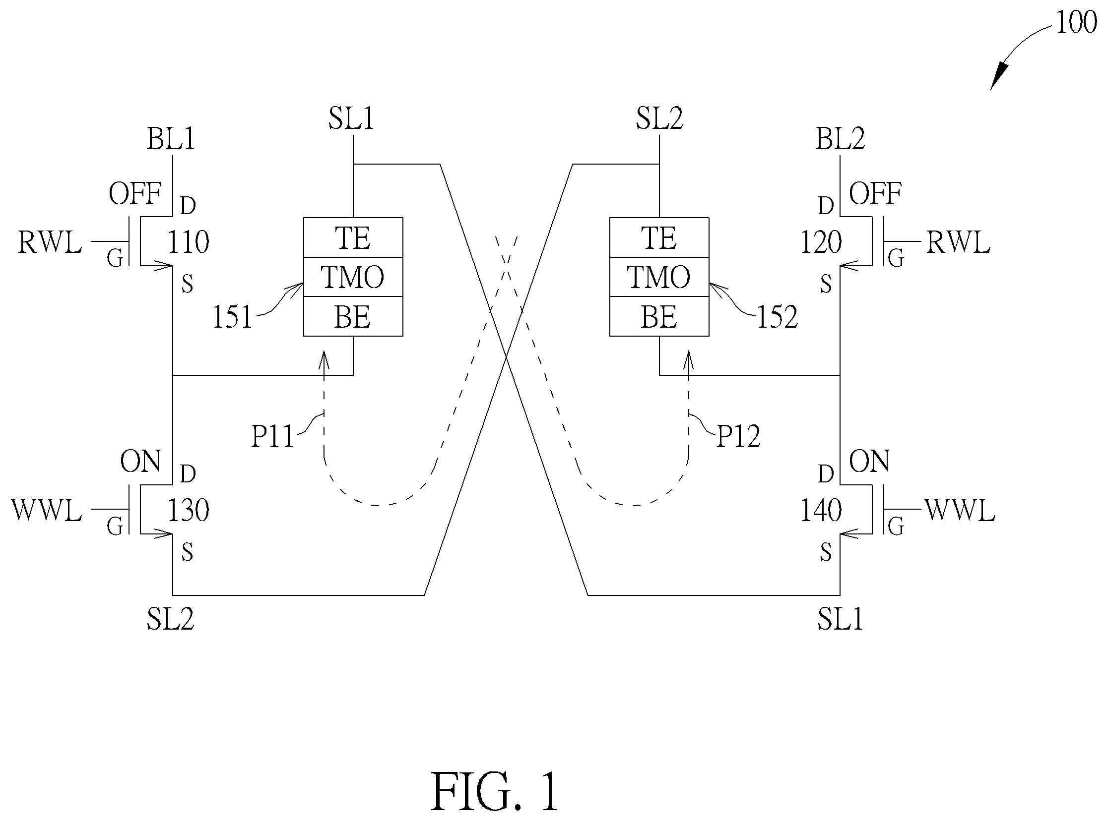
In order to increase the allowable number of times of accessing a memory and reduce the memory area, a memory and a memory mini-array are provided according to embodiments. In the text, when an object A is formed at least partially overlapped with an object B, it means that at least a part of the object A can overlap with at least a part of the object B, or the object A can completely overlap with the object B in a top view. In the text, a conductive via (a.k.a. VIA) can be a conductive connection path formed by drilling a hole and plating the hole with conductive material(s). Each of the memory 100 and the memory 200 mentioned herein can be a bit-cell of a resistive random-access memory (RRAM). and illustrate a memory 100 according to an embodiment. shows a writing operation of the memory 100 . shows a reading operation of the memory 100 . As shown in and , the memory 100 can include a first switch transistor 110 , a second switch transistor 120 , a third switch transistor 130 , a fourth switch transistor 140 , a first resistive memory element 151 and a second resistive memory element 152 . The first switch transistor 110 can include a drain terminal, a source terminal and a gate terminal. The second switch transistor 120 can include a drain terminal, a source terminal and a gate terminal. The third switch transistor 130 can include a drain terminal, a source terminal and a gate terminal, where the drain terminal of the third switch transistor 130 can be coupled to the source terminal of the first switch transistor 110 . The fourth switch transistor 140 can include a drain terminal, a source terminal and a gate terminal, where the drain terminal of the fourth switch transistor 140 can be coupled to the source terminal of the second switch transistor 120 . The first resistive memory element 151 can include a first terminal and a second terminal. The first terminal of the first resistive memory element 151 can be coupled to the source terminal of the fourth switch transistor 140 . The second terminal of the first resistive memory element 151 can be coupled to the source terminal of the first switch transistor 110 . The second resistive memory element 152 can include a first terminal and a second terminal. The first terminal of the second resistive memory element 152 can be coupled to the source terminal of the third switch transistor 130 . The second terminal of the second resistive memory element 152 can be coupled to the source terminal of the second switch transistor 120 . As shown in and , each of the first resistive memory element 151 and the second resistive memory element 152 can include a top electrode TE, a bottom electrode BE and a transition metal oxide layer TMO. The top electrode TE of the first resistive memory element 151 can be coupled to the first terminal of the first resistive memory element 151 . The bottom electrode BE of the first resistive memory element 151 can be coupled to the second terminal of the first resistive memory element 151 . The transition metal oxide layer TMO of the first resistive memory element 151 can be formed between the top electrode TE and the bottom electrode BE of the first resistive memory element 151 . Likewise, the top electrode TE of the second resistive memory element 152 can be coupled to the first terminal of the second resistive memory element 152 . The bottom electrode BE of the second resistive memory element 152 can be coupled to the second terminal of the second resistive memory element 152 . The transition metal oxide layer TMO of the second resistive memory element 152 can be formed between the top electrode TE and the bottom electrode BE of the second resistive memory element 152 . As shown in and , the drain terminal of the first switch transistor 110 can be coupled to a first bit line BL 1 . The gate terminal of the first switch transistor 110 can be coupled to a read word line RWL. The drain terminal of the second switch transistor 120 can be coupled to a second bit line BL 2 . The gate terminal of the second switch transistor 120 can be coupled to the read word line RWL. The gate terminal of the third switch transistor 130 can be coupled to a write word line WWL. The source terminal of the third switch transistor 130 can be coupled to a second source line SL 2 . The gate terminal of the fourth switch transistor 140 can be coupled to the write word line WWL. The source terminal of the fourth switch transistor 140 can be coupled to a first source line SL 1 . As shown in , when the first switch transistor 110 and the second switch transistor 120 are turned off, and the third switch transistor 130 and the fourth switch transistor 140 are turned on, data can be written to the memory 100 through the first source line SL 1 and the second source line SL 2 . As shown in , data can be written to the first resistive memory element 151 and the second resistive memory element 152 through a path P 11 and a path P 12 . In , when writing a logic 0 to the memory 100 , the first source line SL 1 can have a high voltage level (expressed as VH in the text), the second source line SL 2 can have a low voltage level (expressed as VL in the text) lower than the high voltage level VH, the first resistive memory 151 can be set to have a high resistance (expressed as RH in the text), and the second resistive memory element 152 can be set to have a low resistance (expressed as RL in the text) lower than the high resistance RH. In , when writing a logic 1 to the memory 100 , the first source line SL 1 can have the low voltage level VL, the second source line SL 2 can have the high voltage level VH, the first resistive memory 151 can be set to have the low resistance RL, and the second resistive memory element 152 can be set to have the high resistance RH. As shown in , when the first switch transistor 110 and the second switch transistor 120 are turned on, and the third switch transistor 130 and the fourth switch transistor 140 are turned off, data can be read from the memory 100 . As shown in , data can be read from the first resistive memory element 151 and the second resistive memory element 152 through a path P 21 and a path P 22 . In , when reading a logic 0 from the memory 100 , the first source line SL 1 can have the high voltage level VH, and the second source line SL 2 can have the high voltage level VH. In , when reading a logic 1 from the memory 100 , the first source line SL 1 can have the high voltage level VH, and the second source line SL 2 can have the high voltage level VH. The abovementioned writing operation and reading operation of the memory 100 can be described in Table 1. TABLE 1 When writing a The first source line SL1: high voltage level VH In , the first logic 0 The second source line SL2: low voltage level VL switch transistor 110 The first resistive memory element 151: high and the second switch resistance RH transistor 120 are The second resistive memory element 152: low turned off, and the resistance RL third switch transistor When writing a The first source line SL1: low voltage level VL 130 and the fourth logic 1 The second source line SL2: high voltage level VH switch transistor 140 The first resistive memory element 151: low are turned on. resistance RL The second resistive memory element 152: high resistance RH When reading a The first source line SL1: high voltage level VH In , the first logic 0 The second source line SL2: high voltage level VH switch transistor 110 When reading a and the second switch logic 1 transistor 120 are turned on, and the third switch transistor 130 and the fourth switch transistor 140 are turned off. illustrates a circuit including the memory 100 and a memory 200 according to an embodiment. As shown in , the memory 100 can be coupled to the memory 200 , and the memory 200 can be coupled to the first bit line BL 1 , the second bit line BL 2 , the first source line SL 1 and the second source line SL 2 . The circuit area is reduced by coupling the memory 100 to the memory 200 . In , the memory 100 can include the first switch transistor 110 to the fourth switch transistor 140 , the first resistive memory element 151 and the second resistive memory element 152 as mentioned above, and thus is not repeatedly described. Like the first switch transistor 110 to the fourth switch transistor 140 , the first resistive memory element 151 and the second resistive memory element 152 in the memory 100 , the memory 200 can include a fifth switch transistor 210 , a sixth switch transistor 220 , a seventh switch transistor 230 , an eighth switch transistor 240 , a third resistive memory element 251 and a fourth resistive memory element 252 . The couplings of components and operations of the memory 200 can be similar to that of the memory 100 , and is not repeatedly described. As shown in to , same electrodes of the first resistive memory element 151 and the second resistive memory element 152 are formed at same ends, e.g., bottom electrodes BE of the first resistive memory element 151 and the second resistive memory element 152 are coupled to the sources of the first switch transistor 110 and the second switch transistor 120 respectively. Hence, the related connections of the components of the memory 100 are simplified. As shown in , the memory 100 and the memory 200 can share the first bit line BL 1 , the second bit line BL 2 , the first source line SL 1 and the second source line SL 2 . Regarding the layout of semiconductor, the memory 100 and the memory 200 can be integrated in a memory mini-array 800 in the layout as shown in . to illustrate layout diagrams of a manufacturing process of the memory 100 according to an embodiment. In the manufacturing process of the memory 100 , the layout diagrams can be shown sequentially as , , , and according to time sequence. As shown in , the memory 100 can include a diffusion layer DF 1 , a diffusion layer DF 2 , a polysilicon layer PLY 1 , a polysilicon layer PLY 2 , a polysilicon layer PLY 3 and a polysilicon layer PLY 4 . The polysilicon layer PLY 1 , the polysilicon layer PLY 2 , the polysilicon layer PLY 3 and the polysilicon layer PLY 4 can be corresponding to gate terminals of transistors, such as gate terminals of field effect transistors (FETs). The diffusion layers DF 1 and DF 2 can be formed along a first direction D 1 . The polysilicon layer PLY 1 to the polysilicon layer PLY 4 can be formed along a second direction D 2 substantially perpendicular to the first direction D 1 . Each of the polysilicon layer PLY 1 to the polysilicon layer PLY 4 can be formed at least partially overlapped with the diffusion layer DF 1 and the diffusion layer DF 2 . In , the diffusion layer DF 1 and the diffusion layer DF 2 can be formed of a same diffusion layer. For example, a trench can be formed to separate the diffusion layer DF 1 from the diffusion layer DF 2 . As shown in , a plurality of contact elements CT can be formed on the diffusion layers DF 1 , DF 2 . In the top view, each of the contact elements CT can be disposed between two polysilicon layers. If the polysilicon layer PLY 1 in are corresponding to the gate terminals of the first switch transistor 110 and the second switch transistor 120 in , and the polysilicon layer PLY 2 in are corresponding to the gate terminals of the third switch transistor 130 and the fourth switch transistor 140 in , the polysilicon layer PLY 1 can be coupled to the read word line RWL in , and the polysilicon layer PLY 2 in can be coupled to the write word line WWL in . In , a conductive layer M 1 , a plurality of conductive vias VA and a plurality of resistive memory elements RSE 1 , RSE 2 , RSE 3 and RSE 4 can be formed above the diffusion layers DF 1 and DF 2 . One of the resistive memory elements RSE 1 , RSE 2 , RSE 3 and RSE 4 can be corresponding to one of the first resistive memory element 151 , the second resistive memory element 152 , the third resistive memory element 251 and the fourth resistive memory element 252 mentioned in to . As shown in , in the top view, the resistive memory element RSE 1 can be formed at least partially overlapped with the diffusion layer DF 1 and between the polysilicon layer PLY 1 and the polysilicon layer PLY 2 . The resistive memory element RSE 2 can be formed at least partially overlapped with the diffusion layer DF 2 and between the polysilicon layer PLY 1 and the polysilicon layer PLY 2 . In , a conductive layer M 2 can be further formed above the diffusion layer DF 1 and the diffusion layer DF 2 . In the top view, the conductive layer M 2 may not overlap with the resistive memory elements RSE 1 , RSE 2 , RSE 3 and RSE 4 . As shown in , a conductive layer M 3 and a plurality of conductive vias V 2 can be further formed above the conductive layer M 2 and the resistive memory elements RSE 1 to RSE 4 . As shown in , a conductive layer M 4 and a plurality of conductive vias V 3 can be further formed above the conductive layer M 3 . In , the first switch transistor 110 , the second switch transistor 120 , the third switch transistor 130 , the fourth switch transistor 140 , the resistive memory element RSE 1 and the resistive memory element RSE 2 can be used to form a memory including four switch transistors and two resistive memory elements, and the memory can be referred to as a 4T2R memory (e.g. the abovementioned memory 100 ). The fifth switch transistor 210 , the sixth switch transistor 220 , the seventh switch transistor 230 , the eighth switch transistor 240 , the resistive memory element RSE 3 and the resistive memory element RSE 4 can be used to form another memory including four switch transistors and two resistive memory elements, and the memory can be referred to as a 4T2R memory (e.g. the abovementioned memory 200 ). In the layout, the memory 100 and the memory 200 can be used to form the memory mini-array 800 , and the memory 100 and the memory 200 can share the bit lines and source lines as shown in . is a cross-section view of the memory 100 in along the cross-sectional line 9 - 9 ′. As shown in , the memory 100 can include the diffusion layer DF 1 , the diffusion layer DF 2 , a conductive layer M 11 , a conductive layer M 12 , a contact element CT 1 , a contact element CT 2 , a conductive via VA 1 , a conductive via VA 2 , a resistive memory element RSE 1 , a resistive memory element RSE 2 , a conductive layer M 21 , a conductive via V 21 , a conductive via V 22 , a conductive via V 23 , a conductive layer M 31 , a conductive layer M 32 , a conductive layer M 41 , a conductive layer M 42 , a conductive layer M 43 , a conductive layer M 44 and a conductive via V 31 . In , a trench T 1 can be used to separate the diffusion layer DF 1 from the diffusion layer DF 2 . The conductive layer M 11 can be formed at least partially overlapped with the diffusion layer DF 1 . In the top view, the conductive layer M 11 can be formed between the polysilicon layer PLY 1 and the polysilicon layer PLY 2 . The conductive layer M 12 can be formed at least partially overlapped with the diffusion layer DF 2 . In the top view, the conductive layer M 12 can be formed between the polysilicon layer PLY 1 and the polysilicon layer PLY 2 . The conductive layer M 11 and the conductive layer M 12 in can be formed of a same conductive layer, such as the conductive layer M 1 in . As shown in , the conductive layer M 11 can be formed above the diffusion layer DF 1 . The conductive layer M 12 can be formed above the diffusion layer DF 2 . The resistive memory element RSE 1 can be formed above the conductive layer M 11 . The resistive memory element RSE 2 can be formed above the conductive layer M 12 . The contact element CT 1 can be formed between the diffusion layer DF 1 and the conductive layer M 11 , coupled to the diffusion layer DF 1 and the conductive layer M 11 , and at least partially overlapped with the diffusion layer DF 1 . In the top view, the contact element CT 1 can be formed between the polysilicon layer PLY 1 and the polysilicon layer PLY 2 . The contact element CT 2 can be formed between the diffusion layer DF 2 and the conductive layer M 12 , coupled to the diffusion layer DF 2 and the conductive layer M 12 , and at least partially overlapped with the diffusion layer DF 2 . In the top view, the contact element CT 2 can be formed between the polysilicon layer PLY 1 and the polysilicon layer PLY 2 . The contact element CT 1 and the contact element CT 2 can be corresponding to the contact elements CT in . The conductive via VA 1 can be formed between the conductive layer M 11 and the resistive memory element RSE 1 , coupled to the conductive layer M 11 and the resistive memory element RSE 1 , and at least partially overlapped with the resistive memory element RSE 1 . The conductive via VA 2 can be formed between the conductive layer M 12 and the resistive memory element RSE 2 , coupled to the conductive layer M 12 and the resistive memory element RSE 2 , and at least partially overlapped with the resistive memory element RSE 2 . The conductive via VA 1 and the conductive via VA 2 can be corresponding to the conductive vias VA in . The resistive memory element RSE 1 and the resistive memory element RSE 2 can be corresponding to the first resistive memory element 151 and the second resistive memory element 152 in to . As shown in , the conductive layer M 21 can be formed between the resistive memory element RSE 1 and the resistive memory element RSE 2 in the top view. The conductive layer M 31 can be formed above the resistive memory element RSE 1 , and at least partially overlapped with the resistive memory element RSE 1 . The conductive layer M 32 can be formed above the resistive memory element RSE 2 and the conductive layer M 21 . The conductive layer M 32 can be formed at least partially overlapped with the resistive memory element RSE 2 and the conductive layer M 21 . The conductive layer M 21 can be formed of the conductive layer M 2 in . The conductive layer M 31 and the conductive layer M 32 can be formed of a same conductive layer, such as the conductive layer M 3 in . In , the conductive via V 21 can be formed between the resistive memory element RSE 1 and the conductive layer M 31 , coupled to the resistive memory element RSE 1 and the conductive layer M 31 , and at least partially overlapped with the resistive memory element RSE 1 . The conductive via V 22 can be formed between the conductive layer M 21 and the conductive layer M 32 , coupled to the conductive layer M 21 and the conductive layer M 32 , and at least partially overlapped with the conductive layer M 21 . The conductive via V 23 can be formed between the resistive memory element RSE 2 and the conductive layer M 32 , coupled to the resistive memory element RSE 2 and the conductive layer M 32 , and at least partially overlapped with the resistive memory element RSE 2 . The conductive via V 21 , the conductive via V 22 and the conductive via V 23 in can be corresponding to the conductive vias V 2 in . As shown in , the conductive layer M 41 , the conductive layer M 42 , the conductive layer M 43 and the conductive layer M 44 can be formed above the conductive layer M 31 and the conductive layer M 32 . The conductive layer M 41 can be formed at least partially overlapped with the conductive layer M 32 . The conductive via V 31 can be formed between the conductive layer M 32 and the conductive layer M 41 , coupled to the conductive layer M 32 and the conductive layer M 41 , and at least partially overlapped with the conductive layer M 32 . The conductive via V 31 in can be corresponding to the conductive vias V 3 in . The conductive layer M 41 , the conductive layer M 42 , the conductive layer M 43 and the conductive layer M 44 in can be formed of a same conductive layer, such as the conductive layer M 4 in . If the resistive memory element RSE 1 and the resistive memory element RSE 2 are corresponding to the first resistive memory element 151 and the second resistive memory element 152 in and , the conductive layer M 31 in can be coupled to the first source line SL 1 in , the conductive layer M 41 in can be coupled to the second source line SL 2 in , the conductive layer M 11 in can be coupled to the source terminal of the first switch transistor 110 in , and the conductive layer M 12 in can be coupled to the source terminal of the second switch transistor 120 in . illustrates the read window of reading data from a plurality of memories according to an embodiment. In , the horizontal axis represents the currents on the memories, and the vertical axis represents statistical number of memories generated after normalization. On the horizontal axis of , the level HR can be the current level where the resistive memory element of the memory is set to have a high resistance value, and a logic 0 is written to the memory. The level LR can be the current level where the resistive memory element of the memory is set to have a low resistance value, and a logic 1 is written to the memory. The level NR can be a reference current level when a machine is used to measure the memory. If the memory 100 provided by the embodiment is not used, a memory can be read according to the current of a single resistive memory element, and the read operation is corresponding to a single mode operation. Hence, the window corresponding to the high resistance can be WH in , and the window corresponding to the low resistance can be WL in . It can be expressed as WH=|NR−HR| and WL=|LR−NR|. If the memory 100 provided by the embodiment is in use, the memory can be read according to a difference of currents of two resistive memory elements, and the read operation is corresponding to a differential mode operation. Hence, the window corresponding to the high resistance and the low resistance can be expressed as W=|LR−HR|. Since |LR−HR| is greater than |NR−HR|, and |LR−HR| is greater than |LR−NR|, it can be expressed as W>WH and W>WL. As a result, when the memory 100 is in use, the read window is larger. With the larger read window, when the memory 100 is written and read many times (for example, but not limited to, 100,000 times), the data stored in the memory 100 can still be effectively determined as 0 or 1, improving the accuracy of reading the memory and the reliability of the memory. In summary, by using the memory 100 of the embodiment, since the two resistive memory elements are arranged in the same direction, the connections among the components are simplified. The differential mode is used to enlarge the read window, so the accuracy of reading the memory and the reliability of the memory are improved after accessing the memory many times. In addition, through suitable circuit design, layout design and semiconductor structure, two memory cells (e.g. the memory 100 and the memory 200 in ) can be coupled to one another to further reduce the circuit area. Hence, the memory and memory mini-array of embodiments are useful in the field. Those skilled in the art will readily observe that numerous modifications and alterations of the device and method may be made while retaining the teachings of the invention. Accordingly, the above disclosure should be construed as limited only by the metes and bounds of the appended claims.
Figures (10)
Citations
This patent cites (22)
- US9054702
- US9065044
- US9356598
- US9401198
- US9496048
- US10056430
- US10461126
- US11189658
- US2009/0250735
- US2012/0044757
- US2012/0294064
- US2012/0314472
- US2017/0047116
- US2019/0341109
- US2021/0398618
- US2022/0059616
- US2023/0164970
- US115565579
- US10 2018 123 822
- US10 2018 124 716
- US11 2022 003 362
- US2017/064744