Gate Driver and Electronic Apparatus Including the Same
Abstract
A gate driver includes a plurality of stages. Each of the plurality of stages includes a first transistor which transmits an input signal to a control node, a second transistor including a gate connected to an inverting control node, a first terminal which receives a high gate voltage, and a second terminal connected to an output node from which a gate signal is output, a third transistor including a gate connected to the control node, a first terminal which receives a low gate voltage or a clock signal, and a second terminal connected to the output node, and a fourth transistor, which is an NMOS transistor, connected between a terminal of the first transistor and the gate of the sixth transistor, including a gate which receives a global signal having the high gate voltage in an address scan period and the low gate voltage in a self-scan period.
Claims (8)
1 . A gate driver including a plurality of stages, each of the plurality of stages comprising: a first transistor which transmits an input signal to a first control node; a fifth transistor including a gate connected to an inverting control node, a first terminal which receives a high gate voltage, and a second terminal connected to an output node from which a gate signal is output; a sixth transistor including a gate connected to a second control node, a first terminal which receives a first low gate voltage or a clock signal, and a second terminal connected to the output node; and a seventh transistor connected between a terminal of the first transistor and the gate of the sixth transistor, and including a gate which receives a global signal having the high gate voltage in an address scan period and the first low gate voltage in a self-scan period.
8 . An electronic apparatus comprising: a display panel including a plurality of pixels; a gate driver including a plurality of stages which provide a plurality of gate signals to the plurality of pixels; a controller which provides a gate control signal to the gate driver; and a processor which provides a controller control signal to the controller, wherein each of the plurality of stages comprises: a first transistor which transmits an input signal to a first control node; a fifth transistor including a gate connected to an inverting control node, a first terminal which receives a high gate voltage, and a second terminal connected to an output node from which one of the plurality of gate signals is output; a sixth transistor including a gate connected to a second control node, a first terminal which receives a first low gate voltage or a clock signal, and a second terminal connected to the output node; and a seventh transistor connected between a terminal of the first transistor and the gate of the sixth transistor, and including a gate which receives a global signal having the high gate voltage in an address scan period and the first low gate voltage in a self-scan period.
Show 6 dependent claims
2 . The gate driver of claim 1 , wherein each of the plurality of stages further comprises: a second transistor including a gate connected to the second control node, a first terminal which receives the first low gate voltage, and a second terminal connected to the inverting control node; and a third transistor including a gate connected to the first control node, a first terminal which receives the high gate voltage, and a second terminal connected to the inverting control node.
3 . The gate driver of claim 1 , wherein each of the plurality of stages further comprises: a fourth transistor including a gate which receives the first low gate voltage, a first terminal connected to the first control node, and a second terminal connected to the second control node.
4 . The gate driver of claim 3 , wherein the fourth transistor further includes a back gate which receives the high gate voltage.
5 . The gate driver of claim 1 , wherein each of the plurality of stages further comprises: a first capacitor including a first terminal connected to the second control node and a second terminal connected to the output node; and a second capacitor including a first terminal which receives the high gate voltage and a second terminal connected to the inverting control node.
6 . The gate driver of claim 1 , wherein each of the plurality of stages further comprises: a third capacitor including a first terminal connected to the first control node and a second terminal which receives a second low gate voltage.
7 . The gate driver of claim 1 , wherein each of the plurality of stages further comprises: a ninth transistor including a gate connected to the inverting control node, a first terminal which receives the first low gate voltage, and a second terminal connected to the output node.
Full Description
Show full text →
CROSS-REFERENCE TO RELATED APPLICATIONS
This application claims priority under 35 U.S.C. § 119 to Korean Patent Application No. 10-2024-0027846, filed on Feb. 27, 2024, the disclosure of which is incorporated by reference herein in its entirety.
TECHNICAL FIELD
Embodiments relate to a display device. More particularly, embodiments relate to a gate driver with an improved reliability, a display device including the gate driver, and an electronic apparatus including the display device. DISCUSSION OF RELATED ART A display device may include a display panel and a gate driver. The display panel may include a plurality of pixels, and the gate driver may include a plurality of stages that provide gate signals to the pixels. Each of the stages may include a pull-up buffer transistor that outputs a high gate voltage as a gate signal, and a pull-down buffer transistor that outputs a low gate voltage as the gate signal. The pull-down buffer transistor may be turned on in response to a voltage of a control node. When the display device is driven at a low frequency, a turn-on voltage may be provided to the control node for a relatively long time, and the pull-down buffer transistor may be turned on for a long time. When a leakage current occurs from the control node, the voltage of the control node may rise, and thus, the gate signal may rise.
SUMMARY
Embodiments of the present disclosure provide a gate driver having increased reliability and an electronic apparatus including the gate driver. According to an embodiment of the present disclosure, in a gate driver including a plurality of stages, each of the plurality of stages includes a first transistor which transmits an input signal to a control node, a second transistor including a gate connected to an inverting control node, a first terminal which receives a high gate voltage, and a second terminal connected to an output node from which a gate signal is output, a third transistor including a gate connected to the control node, a first terminal which receives a low gate voltage or a clock signal, and a second terminal connected to the output node, and a seventh transistor, which is an n-channel metal oxide semiconductor (NMOS) transistor, connected between a second terminal of the first transistor and the gate of the sixth transistor, and including a gate which receives a global signal having the high gate voltage in an address scan period and the low gate voltage in a self-scan period. In an embodiment, each of the plurality of stages further includes a fifth transistor including a gate connected to the control node, a first terminal which receives the low gate voltage, and a second terminal connected to the inverting control node, and a sixth transistor including a gate connected to the control node, a first terminal which receives the high gate voltage, and a second terminal connected to the inverting control node. In an embodiment, each of the plurality of stages further includes a fifth transistor which divides the control node into a first control node and a second control node, the fifth transistor including a gate which receives the low gate voltage, a first terminal connected to the first control node, and a second terminal connected to the second control node. In an embodiment, the fifth transistor further includes a back gate which receives the high gate voltage. In an embodiment, each of the plurality of stages further includes a first capacitor including a first terminal connected to the control node and a second terminal connected to the output node, and a second capacitor including a first terminal which receives the high gate voltage and a second terminal connected to the inverting control node. In an embodiment, each of the plurality of stages further includes a capacitor including a first terminal connected to the control node and a second terminal which receives the low gate voltage. In an embodiment, each of the plurality of stages further includes a fifth transistor including a gate connected to the inverting control node, a first terminal which receives the low gate voltage, and a second terminal connected to the output node. According to an embodiment of the present disclosure, in a gate driver including a plurality of stages, each of the plurality of stages includes a first transistor, which is an NMOS transistor, which transmits an input signal to a control node, and includes a gate which receives a global signal having a clock signal in an address scan period and a low gate voltage in a self-scan period, a second transistor including a gate connected to an inverting control node, a first terminal which receives a high gate voltage, and a second terminal connected to an output node from which a gate signal is output, and a third transistor including a gate connected to the control node, a first terminal which receives the low gate voltage or the clock signal, and a second terminal connected to the output node. In an embodiment, each of the plurality of stages further includes a fourth transistor including a gate connected to the control node, a first terminal which receives the low gate voltage, and a second terminal connected to the inverting control node, and a fifth transistor including a gate connected to the control node, a first terminal which receives the high gate voltage, and a second terminal connected to the inverting control node. In an embodiment, each of the plurality of stages further includes a fourth transistor which divides the control node into a first control node and a second control node, the fourth transistor including a gate which receives the low gate voltage, a first terminal connected to the first control node, and a second terminal connected to the second control node. In an embodiment, the fourth transistor further includes a back gate which receives the high gate voltage. In an embodiment, each of the plurality of stages further includes a first capacitor including a first terminal connected to the control node and a second terminal connected to the output node, and a second capacitor including a first terminal which receives the high gate voltage and a second terminal connected to the inverting control node. In an embodiment, each of the plurality of stages further includes a capacitor including a first terminal connected to the control node and a second terminal which receives the low gate voltage. In an embodiment, each of the plurality of stages further includes a fourth transistor including a gate connected to the inverting control node, a first terminal which receives the low gate voltage, and a second terminal connected to the output node. According to an embodiment of the present disclosure, in a gate driver including first to n th (where n is a positive integer greater than 1) stages, a k th (where k is a positive integer greater than 1 and less than n) stage among the first to n th stages includes a first transistor which transmits an input signal to a control node, a second transistor including a gate connected to an inverting control node, a first terminal which receives a high gate voltage, and a second terminal connected to an output node from which a gate signal is output, a third transistor including a gate connected to the control node, a first terminal which receives a low gate voltage or a clock signal, and a second terminal connected to the output node, and a fourth transistor, which is an NMOS transistor, connected between a terminal of the first transistor and the gate of the third transistor, and including a gate which receives a voltage of the control node of one of a k−1 th stage and the k th stage. In an embodiment, the k th stage further includes a fifth transistor, which is an NMOS transistor, including a gate which receives a voltage of the control node of another one of the k−1 th stage and the k th stage, a first terminal connected to a first terminal of the fourth transistor, and a second terminal connected to a second terminal of the fourth transistor. In an embodiment, the k th stage further includes a fifth transistor including a gate connected to the control node, a first terminal which receives the low gate voltage, and a second terminal connected to the inverting control node, and a sixth transistor including a gate connected to the control node, a first terminal which receives the high gate voltage, and a second terminal connected to the inverting control node. In an embodiment, the k th stage further includes a fifth transistor which divides the control node into a first control node and a second control node, the fifth transistor including a gate which receives the low gate voltage, a first terminal connected to the first control node, and a second terminal connected to the second control node. In an embodiment, the fifth transistor further includes a back gate which receives the high gate voltage. In an embodiment, the k th stage further includes a first capacitor including a first terminal connected to the control node and a second terminal connected to the output node, and a second capacitor including a first terminal which receives the high gate voltage and a second terminal connected to the inverting control node. According to an embodiment of the present disclosure, an electronic apparatus includes a display panel including a plurality of pixels, a gate driver including a plurality of stages which provide a plurality of gate signals to the plurality of pixels, a controller which provides a gate control signal to the gate driver, and a processor which provides a controller control signal to the controller. Each of the plurality of stages includes a first transistor which transmits an input signal to a control node, a second transistor including a gate connected to an inverting control node, a first terminal which receives a high gate voltage, and a second terminal connected to an output node from which one of the plurality of gate signals is output, a third transistor including a gate connected to the control node, a first terminal which receives a low gate voltage or a clock signal, and a second terminal connected to the output node, and a fourth transistor, which is an n-channel metal oxide semiconductor (NMOS) transistor, connected between a terminal of the first transistor and the gate of the third transistor, and including a gate which receives a global signal having the high gate voltage in an address scan period and the low gate voltage in a self-scan period. In a gate driver according to embodiments of the present disclosure, an NMOS transistor may be disposed between the input terminal and the control node. As a result, a leakage current may not occur from the gate of the pull-down buffer transistor in the self-scan period. Accordingly, the gate signal may be maintained at the low gate voltage in the self-scan period, and the reliability of the gate driver may be increased.
BRIEF DESCRIPTION OF THE DRAWINGS
The above and other features of the present disclosure will become more apparent by describing in detail embodiments thereof with reference to the accompanying drawings. is a block diagram showing a display device according to an embodiment. is a view for describing a driving method of the display device of . is a circuit diagram showing an example of a pixel included in the display device of . is a view for describing a driving method of the pixel of . is a block diagram showing a gate driver according to an embodiment. is a circuit diagram showing an example of a k th stage included in the gate driver of . is a view for describing a driving method of the k th stage of . is a circuit diagram showing an example of a k th stage included in the gate driver of . is a circuit diagram showing an example of a k th stage included in the gate driver of . is a view for describing a driving method of the k th stage of . is a circuit diagram showing an example of a k th stage included in the gate driver of . is a circuit diagram showing an example of a k th stage included in the gate driver of . is a view for describing a driving method of the k th stage of . is a circuit diagram showing an example of a k th stage included in the gate driver of . is a block diagram showing an electronic apparatus according to an embodiment.
DETAILED
DESCRIPTION OF THE EMBODIMENTS
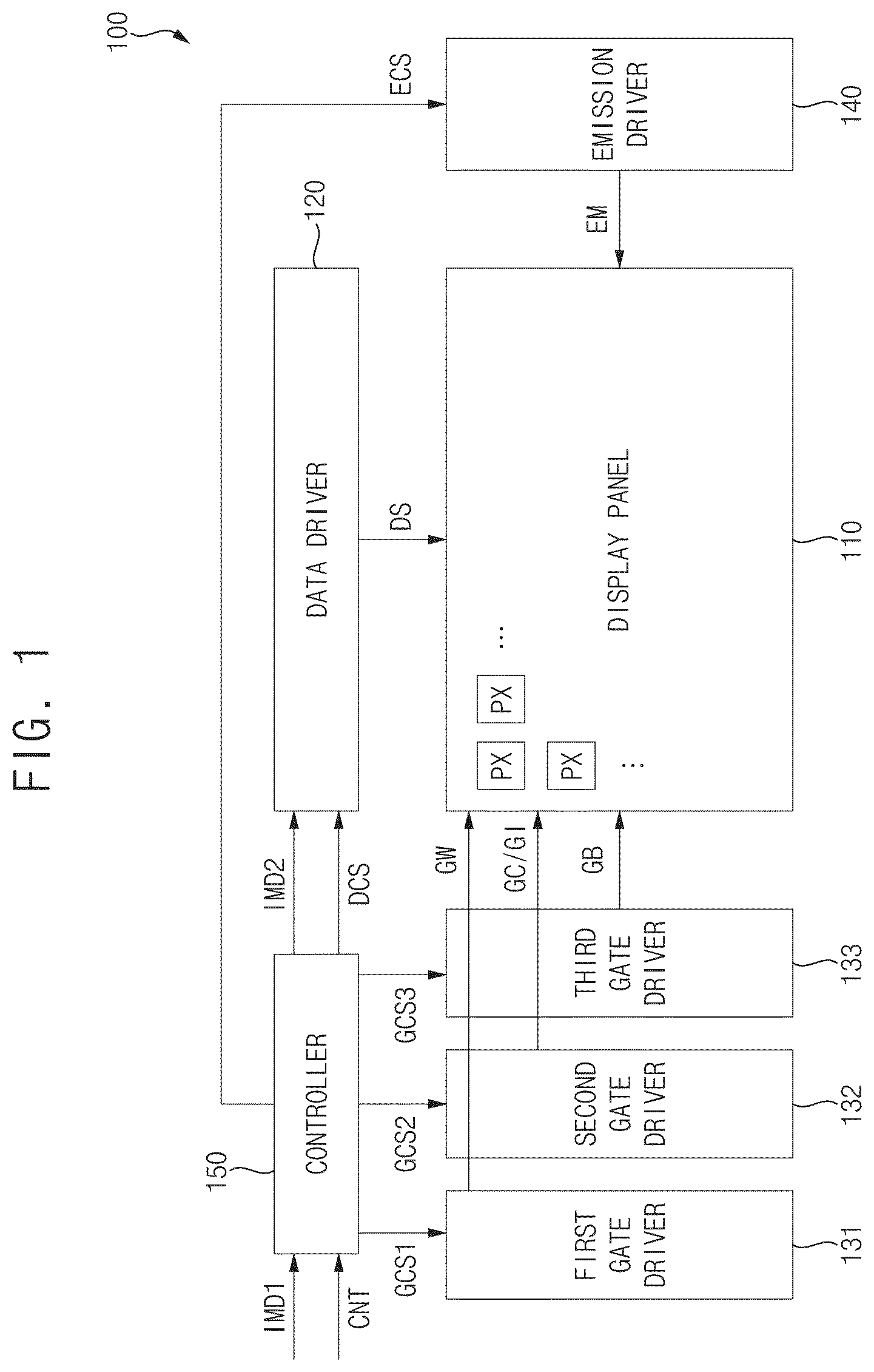
Embodiments of the present disclosure will be described more fully hereinafter with reference to the accompanying drawings. Like reference numerals may refer to like elements throughout the accompanying drawings. It will be understood that the terms “first,” “second,” “third,” etc. are used herein to distinguish one element from another, and the elements are not limited by these terms. Thus, a “first” element in an embodiment may be described as a “second” element in another embodiment. It should be understood that descriptions of features or aspects within each embodiment should typically be considered as available for other similar features or aspects in other embodiments, unless the context clearly indicates otherwise. As used herein, the singular forms “a”, “an” and “the” are intended to include the plural forms as well, unless the context clearly indicates otherwise. The term “about” as used herein is inclusive of the stated value and means within an acceptable range of deviation for the particular value as determined by one of ordinary skill in the art, considering the measurement in question and the error associated with measurement of the particular quantity (e.g., the limitations of the measurement system). For example, “about” may mean within one or more standard deviations as understood by one of the ordinary skill in the art. Further, it is to be understood that while parameters may be described herein as having “about” a certain value, according to embodiments, the parameter may be exactly the certain value or approximately the certain value within a measurement error as would be understood by a person having ordinary skill in the art. is a block diagram showing a display device 100 according to an embodiment. Referring to , the display device 100 may include a display panel 110 , a data driver 120 , first to third gate drivers 131 , 132 , and 133 , an emission driver 140 , and a controller 150 . Each gate driver may also be referred to as a gate driver circuit. The display panel 110 may include a plurality of pixels PX. Each of the pixels PX may display an image based on a first gate signal GW, a second gate signal GC, a third gate signal GI, a fourth gate signal GB, an emission signal EM, and a data signal DS. The data driver 120 may provide the data signal DS to the pixels PX. The data driver 120 may generate the data signal DS based on second image data IMD 2 and a data control signal DCS. The second image data IMD 2 may include a plurality of grayscale values corresponding to the pixels PX. The data control signal DCS may include, for example, an output data enable signal, a horizontal start signal, a load signal, etc. The first gate driver 131 may provide the first gate signal GW to the pixels PX. The first gate driver 131 may generate the first gate signal GW based on a first gate control signal GCS 1 . The first gate control signal GCS 1 may include, for example, a first gate clock signal, a first gate start signal, etc. The second gate driver 132 may provide the second gate signal GC and the third gate signal GI to the pixels PX. The second gate driver 132 may generate the second gate signal GC and the third gate signal GI based on a second gate control signal GCS 2 . The second gate control signal GCS 2 may include, for example, a second gate clock signal, a second gate start signal, etc. The third gate driver 133 may provide the fourth gate signal GB to the pixels PX. The third gate driver 133 may generate the fourth gate signal GB based on a third gate control signal GCS 3 . The third gate control signal GCS 3 may include, for example, a third gate clock signal, a third gate start signal, etc. The emission driver 140 may provide the emission signal EM to the pixels PX. The emission driver 140 may generate the emission signal EM based on an emission control signal ECS. The emission control signal ECS may include, for example, an emission clock signal, an emission start signal, etc. The controller 150 may control an operation (or driving) of the data driver 120 , operations (or driving) of the first to third gate drivers 131 , 132 , and 133 , and an operation (or driving) of the emission driver 140 . The controller 150 may output the second image data IMD 2 and the data control signal DCS to the data driver 120 , may output the first to third gate control signals GCS 1 , GCS 2 , and GCS 3 to the first to third gate drivers 131 , 132 , and 133 , and may output the emission control signal ECS to the emission driver 140 . The controller 150 may generate the second image data IMD 2 , the data control signal DCS, the first to third gate control signals GCS 1 , GCS 2 , and GCS 3 , and the emission control signal ECS based on first image data IMD 1 and a controller control signal CNT. The first image data IMD 1 may include a plurality of grayscale values corresponding to the pixels PX. The controller control signal CNT may include, for example, a master clock signal, a vertical start signal, a horizontal start signal, an input data enable signal, etc. is a view for describing a driving method of the display device 100 of . Referring to , a frame period of the display device 100 may include an address scan period AS and at least one self-scan period SS. The address scan period AS may be defined as a period in which the data signal DS is applied to the display panel 110 . In the address scan period AS, the display device 100 may display an image based on the data signal DS applied in the address scan period AS. The self-scan period SS may be defined as a period in which the data signal DS is not applied to the display panel 110 . In the self-scan period SS, the display device 100 may display an image based on the data signal DS applied in the address scan period AS. The display device 100 may change a driving frequency (or refresh rate) of the display device 100 by adjusting the number of self-scan periods SS included in the frame period. As the number of self-scan periods SS included in the frame period decreases, the driving frequency of the display device 100 may increase. As the number of self-scan periods SS included in the frame period increases, the driving frequency of the display device 100 may decrease. In an embodiment, as shown in , when a first frame period FR 1 includes one self-scan period SS, a second frame period FR 2 includes two self-scan periods SS, and a third frame period FR 3 includes three self-scan periods SS, a driving frequency of the second frame period FR 2 may be less than a driving frequency of the first frame period FR 1 , and a driving frequency of the third frame period FR 3 may be less than the driving frequency of the second frame period FR 2 . For example, the driving frequency of the first frame period FR 1 may be about 120 Hz, the driving frequency of the second frame period FR 2 may be about 80 Hz, and the driving frequency of the third frame period FR 3 may be about 60 Hz. is a circuit diagram showing an example of a pixel PX included in the display device 100 of . Referring to , the pixel PX may receive the data signal DS, the first gate signal GW, the second gate signal GC, the third gate signal GI, the fourth gate signal GB, the emission signal EM, a first initialization voltage VINT, a second initialization voltage VAINT, a first power voltage ELVDD, and a second power voltage ELVSS. The pixel PX may include a driving transistor M 1 , a write transistor M 2 , a compensation transistor M 3 , an initialization transistor M 4 , a first emission transistor M 5 , a second emission transistor M 6 , a bypass transistor M 7 , a bias transistor M 8 , a storage capacitor CST, and a light emitting element EL. The driving transistor M 1 may include a gate connected to a first node N 1 , a first terminal connected to a second node N 2 , and a second terminal connected to a third node N 3 . The driving transistor M 1 may generate a driving current corresponding to a voltage difference between the first node N 1 and the second node N 2 . The write transistor M 2 may include a gate that receives the first gate signal GW, a first terminal that receives the data signal DS, and a second terminal connected to the second node N 2 . The write transistor M 2 may transmit the data signal DS to the second node N 2 in response to the first gate signal GW. The compensation transistor M 3 may include a gate that receives the second gate signal GC, a first terminal connected to the third node N 3 , and a second terminal connected to the first node N 1 . The compensation transistor M 3 may connect the first node N 1 and the third node N 3 in response to the second gate signal GC. The initialization transistor M 4 may include a gate that receives the third gate signal GI, a first terminal that receives the first initialization voltage VINT, and a second terminal connected to the first node N 1 . The initialization transistor M 4 may transmit the first initialization voltage VINT to the first node N 1 in response to the third gate signal GI. The first emission transistor M 5 may include a gate that receives the emission signal EM, a first terminal that receives the first power voltage ELVDD, and a second terminal connected to the second node N 2 . The first emission transistor M 5 may transmit the first power voltage ELVDD to the second node N 2 in response to the emission signal EM. The second emission transistor M 6 may include a gate that receives the emission signal EM, a first terminal connected to the third node N 3 , and a second terminal connected to a fourth node N 4 . The second emission transistor M 6 may connect the third node N 3 and the fourth node N 4 in response to the emission signal EM. The bypass transistor M 7 may include a gate that receives the fourth gate signal GB, a first terminal that receives the second initialization voltage VAINT, and a second terminal connected to the fourth node N 4 . The bypass transistor M 7 may transmit the second initialization voltage VAINT to the fourth node N 4 in response to the fourth gate signal GB. The bias transistor M 8 may include a gate that receives the fourth gate signal GB, a first terminal that receives a bias voltage VBIAS, and a second terminal connected to the second node N 2 . The bias transistor M 8 may transmit the bias voltage VBIAS to the second node N 2 in response to the fourth gate signal GB. In an embodiment, each of the driving transistor M 1 , the write transistor M 2 , the first emission transistor M 5 , the second emission transistor M 6 , the bypass transistor M 7 , and the bias transistor M 8 may be a p-channel metal oxide semiconductor (PMOS) transistor, and each of the compensation transistor M 3 and the initialization transistor M 4 may be an n-channel metal oxide semiconductor (NMOS) transistor. The storage capacitor CST may include a first terminal that receives the first power voltage ELVDD and a second terminal connected to the first node N 1 . The storage capacitor CST may store a voltage of the first node N 1 . The light emitting element EL may include a first terminal (e.g., an anode) connected to the fourth node N 4 and a second terminal (e.g., a cathode) that receives the second power voltage ELVSS. The light emitting element EL may emit light corresponding to the driving current generated from the driving transistor M 1 . In an embodiment, the light emitting element EL may be an organic light emitting diode. In an embodiment, the light emitting element EL may be any one of an inorganic light emitting diode, a micro light emitting diode, and a quantum dot light emitting diode. is a view for describing a driving method of the pixel PX of . Referring to , the frame period FR may include an address scan period AS and at least one self-scan period SS. The address scan period AS may include an initialization period PI, a compensation period PC, a write period PW, a first bypass period PB 1 , and a first emission period PE 1 . The self-scan period SS may include a second bypass period PB 2 and a second emission period PE 2 . The second gate signal GC may be a signal in which the third gate signal GI is shifted by a predetermined amount of time. In the initialization period PI, the initialization transistor M 4 may be turned on in response to the third gate signal GI having a high voltage level, and the first initialization voltage VINT may be transmitted to the first node N 1 . Accordingly, the gate of the driving transistor M 1 may be initialized with the first initialization voltage VINT. In the compensation period PC, the compensation transistor M 3 may be turned on in response to the second gate signal GC having a high voltage level, and the third node N 3 and the first node N 1 may be connected. Accordingly, the driving transistor M 1 may be diode-connected. In the write period PW, the write transistor M 2 may be turned on in response to the first gate signal GW having a low voltage level, and the data signal DS may be transmitted to the second node N 2 . The data signal DS in which a threshold voltage of the driving transistor M 1 is reflected may be applied to the first node N 1 by the diode-connected driving transistor M 1 . In the first bypass period PB 1 , the bypass transistor M 7 may be turned on in response to the fourth gate signal GB having a low voltage level, and the second initialization voltage VAINT may be transmitted to the fourth node N 4 . Accordingly, the first terminal of the light emitting element EL may be initialized with the second initialization voltage VAINT. Further, the bias transistor M 8 may be turned on in response to the fourth gate signal GB having the low voltage level in the first bypass period PB 1 , and the bias voltage VBIAS may be transmitted to the second node N 2 . Accordingly, the driving transistor M 1 may be on-biased by the bias voltage VBIAS. In the first emission period PE 1 , the first emission transistor M 5 and the second emission transistor M 6 may be turned on in response to the emission signal EM having a low voltage level, and a current path may be formed between a line transmitting the first power voltage ELVDD and a line transmitting the second power voltage ELVSS. Accordingly, the driving transistor M 1 may generate the driving current corresponding to the voltage difference between the first node N 1 and the second node N 2 , and the light emitting element EL may emit light with a luminance corresponding to the driving current. In the second bypass period PB 2 , the bypass transistor M 7 may be turned on in response to the fourth gate signal GB having the low voltage level, and the second initialization voltage VAINT may be transmitted to the fourth node N 4 . Accordingly, the first terminal of the light emitting element EL may be initialized with the second initialization voltage VAINT. Further, in the second bypass period PB 2 , the bias transistor M 8 may be turned on in response to the fourth gate signal GB having the low voltage level, and the bias voltage VBIAS may be transmitted to the second node N 2 . Accordingly, the driving transistor M 1 may be on-biased by the bias voltage VBIAS. In the second emission period PE 2 , the first emission transistor M 5 and the second emission transistor M 6 may be turned on in response to the emission signal EM having the low voltage level, and a current path may be formed between the line transmitting the first power voltage ELVDD and the line transmitting the second power voltage ELVSS. Accordingly, the driving transistor M 1 may generate the driving current corresponding to the voltage difference between the first node N 1 and the second node N 2 , and the light emitting element EL may emit light with a luminance corresponding to the driving current. is a block diagram showing a gate driver 10 according to an embodiment. Referring to , the gate driver 10 may receive a first clock signal CK 1 , a second clock signal CK 2 , a high gate voltage VGH, a low gate voltage VGL, and a gate start signal FLM, and may output first to n th (n is a positive integer greater than 1) gate signals GS[ 1 ], GS[ 2 ], . . . , GS[n−1], and GS[n]. The second clock signal CK 2 may be a signal in which the first clock signal CK 1 is shifted by half a period (e.g., 1 horizontal time period) of the first clock signal CK 1 . The high gate voltage VGH may be a turn-off voltage of the PMOS transistor and a turn-on voltage of the NMOS transistor. The low gate voltage VGL may be a turn-on voltage of the PMOS transistor and a turn-off voltage of the NMOS transistor. In an embodiment, the gate driver 10 may correspond to the second gate driver 132 of . In this case, the first to n th gate signals GS[ 1 ], GS[ 2 ], . . . , GS[n−1], and GS[n] may correspond to the second gate signal GC or the third gate signal GI. The gate driver 10 may include first to n th stages ST[ 1 ], ST[ 2 ], . . . , ST[n−1], and ST[n]. Each of the first to n th stages ST[ 1 ], ST[ 2 ], . . . , ST[n−1], and ST[n] may receive the high gate voltage VGH and the low gate voltage VGL. Each of the first to n th stages ST[ 1 ], ST[ 2 ], . . . , ST[n−1], and ST[n] may receive the first clock signal CK 1 or the second clock signal CK 2 . In an embodiment, each of odd-numbered stages ST[ 1 ], . . . , ST[n−1] may receive the first clock signal CK 1 , and each of even-numbered stages ST[ 2 ], . . . , ST[n] may receive the second clock signal CK 2 . The first stage ST[ 1 ] may receive the gate start signal FLM, and each of the second to n th stages ST[ 2 ], . . . , ST[n−1], and ST[n] may receive a gate signal output from the previous stage. The first to n th stages ST[ 1 ], ST[ 2 ], . . . , ST[n−1], and ST[n] may output the first to n th gate signals GS[ 1 ], GS[ 2 ], . . . , GS[n−1], and GS[n], respectively. is a circuit diagram showing an example of a k th stage ST[k] included in the gate driver 10 of . Referring to , the k th stage ST[k] (k is a positive integer greater than or equal to 1 and less than or equal to n) may receive an input signal INS, a clock signal CLK, the high gate voltage VGH, the low gate voltage VGL, and a global signal GLS 1 , and may output a k th gate signal GS[k]. The low gate voltage VGL may include a first low gate voltage VGL 1 and a second low gate voltage VGL 2 . When the k th stage ST[k] is the first stage ST[ 1 ], the input signal INS may be the gate start signal FLM. When the k th stage ST[k] is one of the second to n th stages ST[ 2 ], . . . , ST[n−1], and ST[n], the input signal INS may be a k−1 th gate signal output from a k−1 th stage. When the k th stage ST[k] is one of the odd-numbered stages ST[ 1 ], . . . , ST[n−1], the clock signal CLK may be the first clock signal CK 1 . When the k th stage ST[k] is one of the even-numbered stages ST[ 2 ], . . . , ST[n], the clock signal CLK may be the second clock signal CK 2 . The k th stage ST[k] may include a first transistor T 1 , a second transistor T 2 , a third transistor T 3 , a fourth transistor T 4 , a fifth transistor T 5 , a sixth transistor T 6 , a seventh transistor T 7 , a first capacitor C 1 , a second capacitor C 2 , and a third capacitor C 3 . The first transistor T 1 may transmit the input signal INS to a control node NQ. In an embodiment, the first transistor T 1 may include a gate that receives the clock signal CLK, a first terminal connected to an input terminal TIN, and a second terminal. The input signal INS may be input to the input terminal TIN. The first transistor T 1 may transmit the input signal INS in response to the clock signal CLK. The second transistor T 2 may include a gate connected to the control node NQ (e.g., a second control node NQ 2 ), a first terminal that receives the first low gate voltage VGL 1 , and a second terminal connected to an inverting control node NQB. In an embodiment, the second transistor T 2 may further include a back gate that receives the second low gate voltage VGL 2 . The second transistor T 2 may transmit the first low gate voltage VGL 1 to the inverting control node NQB in response to a voltage of the control node NQ. The third transistor T 3 may include a gate connected to the control node NQ (e.g., a first control node NQ 1 ), a first terminal that receives the high gate voltage VGH, and a second terminal connected to the inverting control node NQB. The third transistor T 3 may transmit the high gate voltage VGH to the inverting control node NQB in response to the voltage of the control node NQ. The fourth transistor T 4 may divide the control node NQ into the first control node NQ 1 and the second control node NQ 2 . The fourth transistor T 4 may include a gate that receives the first low gate voltage VGL 1 , a first terminal connected to the first control node NQ 1 , and a second terminal connected to the second control node NQ 2 . As the first low gate voltage VGL 1 is applied to the gate of the fourth transistor T 4 , the fourth transistor T 4 may be an always-on transistor (AOT). The fifth transistor T 5 may include a gate connected to the inverting control node NQB, a first terminal that receives the high gate voltage VGH, and a second terminal connected to an output node NO. The gate signal GS[k] may be output from the output node NO. The fifth transistor T 5 may transmit the high gate voltage VGH to the output node NO in response to a voltage of the inverting control node NQB. The fifth transistor T 5 may be referred to as a pull-up buffer transistor. The sixth transistor T 6 may include a gate connected to the second control node NQ 2 , a first terminal that receives the first low gate voltage VGL 1 or the clock signal CLK, and a second terminal connected to the output node NO. The sixth transistor T 6 may transmit the first low gate voltage VGL 1 to the output node NO in response to a voltage of the second control node NQ 2 . The sixth transistor T 6 may be referred to as a pull-down buffer transistor. Although illustrates an embodiment in which the first terminal of the sixth transistor T 6 receives the first low gate voltage VGL 1 , the present disclosure is not limited thereto. For example, in an embodiment, the first terminal of the sixth transistor T 6 may receive the clock signal CLK. The seventh transistor T 7 may be an NMOS transistor. The seventh transistor T 7 may be connected between the second terminal of the first transistor T 1 and the gate of the sixth transistor T 6 , and may include a gate that receives the global signal GLS 1 . In an embodiment, the seventh transistor T 7 may further include a back gate that receives the global signal GLS 1 . In an embodiment, as shown in , the first terminal of the seventh transistor T 7 may be connected to the second terminal of the first transistor T 1 , and the second terminal of the seventh transistor T 7 may be connected to the first control node NQ 1 . In this case, the seventh transistor T 7 may connect the second terminal of the first transistor T 1 and the first control node NQ 1 in response to the global signal GLS 1 . In an embodiment, the first terminal of the seventh transistor T 7 may be connected to the second terminal of the fourth transistor T 4 , and the second terminal of the seventh transistor T 7 may be connected to the second control node NQ 2 . In this case, the seventh transistor T 7 may connect the second terminal of the fourth transistor T 4 and the second control node NQ 2 in response to the global signal GLS 1 . The first capacitor C 1 may include a first terminal connected to the second control node NQ 2 and a second terminal connected to the output node NO. The first capacitor C 1 may store a voltage difference between the second control node NQ 2 and the output node NO. The second capacitor C 2 may include a first terminal that receives the high gate voltage VGH and a second terminal connected to the inverting control node NQB. The second capacitor C 2 may store the voltage of the inverting control node NQB. The third capacitor C 3 may include a first terminal connected to the first control node NQ 1 and a second terminal that receives the second low gate voltage VGL 2 . The third capacitor C 3 may store the voltage of the first control node NQ 1 . In an embodiment, each of the first transistor T 1 , the third transistor T 3 , the fourth transistor T 4 , the fifth transistor T 5 , and the sixth transistor T 6 may be a PMOS transistor, and the second transistor T 2 may be an NMOS transistor. However, the present disclosure is not limited thereto. For example, in an embodiment, at least one of the first transistor T 1 , the third transistor T 3 , the fourth transistor T 4 , the fifth transistor T 5 , and the sixth transistor T 6 may be an NMOS transistor, and the second transistor T 2 may be a PMOS transistor. is a view for describing a driving method of the k th stage ST[k] of . Referring to , the global signal GLS 1 may have the high gate voltage VGH in the address scan period AS, and may have the low gate voltage VGL in the self-scan period SS. The seventh transistor T 7 may be turned on in response to the global signal GLS 1 having the high gate voltage VGH in the address scan period AS, and the second terminal of the first transistor T 1 may be connected to the control node NQ. Accordingly, the input signal INS may be transmitted to the control node NQ in the address scan period AS, and the gate signal GS[k] having the high gate voltage VGH may be output in response to the high gate voltage VGH of the control node NQ and the low gate voltage VGL of the inverted control node NQB between a first time point TP 1 and a second time point TP 2 . In an embodiment, the seventh transistor T 7 may be turned off in response to the global signal GLS 1 having the low gate voltage VGL in the self-scan period SS, and the second terminal of the first transistor T 1 is not connected to the control node NQ. Accordingly, in an embodiment, the input signal INS is not transmitted to the control node NQ in the self-scan period SS, and the gate signal GS[k] having the low gate voltage VGL may be output in response to the low gate voltage VGL of the control node NQ and the high gate voltage VGH of the inverting control node NQB. The control node NQ may have the low gate voltage VGL for a relatively long time in the self-scan period SS. The magnitude of the leakage current of the NMOS transistor may be less than the magnitude of the leakage current of the PMOS transistor. When the k th stage ST[k] does not include the seventh transistor T 7 , a leakage current may occur from the gate of the sixth transistor T 6 through the first and fourth transistors T 1 and T 4 , which are the PMOS transistors connected to the control node NQ in the self-scan period SS, and accordingly, the voltage of the control node NQ may rise from the low gate voltage VGL, and the gate signal GS[k] may rise from the low gate voltage VGL. In this case, as the voltage of the gate signal GS[k] rises in the self-scan period SS, the reliability of the gate driver 10 may be decreased. In an embodiment of the present disclosure, because the k th stage ST[k] includes the seventh transistor T 7 , which is an NMOS transistor disposed between the input terminal TIN and the control node NQ, a leakage current may be prevented from occurring at the gate of the sixth transistor T 6 in the self-scan period SS. As a result, the voltage of the control node NQ may be maintained at the low gate voltage VGL, and the gate signal GS[k] may remain stable at the low gate voltage VGL. By ensuring the gate signal GS[k] stays at the low gate voltage VGL in the self-scan period SS, the reliability of the gate driver 10 may be increased. is a circuit diagram showing an example of the k th stage ST[k] included in the gate driver 10 of . For convenience of explanation, a further description of components of the k th stage ST[k] described with reference to , which are substantially the same as or similar to those of the k th stage ST[k] described with reference to , will be omitted. Referring to , the k th stage ST[k] may include a first transistor T 1 , a second transistor T 2 , a third transistor T 3 , a fourth transistor T 4 , a fifth transistor T 5 , a sixth transistor T 6 , a seventh transistor T 7 , a ninth transistor T 9 , a first capacitor C 1 , a second capacitor C 2 , and a third capacitor C 3 . In an embodiment, the fourth transistor T 4 may further include a back gate that receives the high gate voltage VGH. The ninth transistor T 9 may include a gate connected to the inverting control node NQB, a first terminal that receives the first low gate voltage VGL 1 , and a second terminal connected to the output node NO. In an embodiment, the ninth transistor T 9 may further include a back gate that receives the second low gate voltage VGL 2 . The ninth transistor T 9 may transmit the first low gate voltage VGL 1 to the output node NO in response to the voltage of the inverting control node NQB. The ninth transistor T 9 may be referred to as an auxiliary pull-down buffer transistor. is a circuit diagram showing an example of the k th stage ST[k] included in the gate driver 10 of . For convenience of explanation, a further description of components of the k th stage ST[k] described with reference to , which are substantially the same as or similar to those of the k th stage ST[k] described with reference to , will be omitted. Referring to , the k th stage ST[k] may receive an input signal INS, the high gate voltage VGH, the low gate voltage VGL, and a global signal GLS 2 , and may output a k th gate signal GS[k]. The k th stage ST[k] may include a first transistor T 1 , a second transistor T 2 , a third transistor T 3 , a fourth transistor T 4 , a fifth transistor T 5 , a sixth transistor T 6 , a first capacitor C 1 , a second capacitor C 2 , and a third capacitor C 3 . The first transistor T 1 may be an NMOS transistor. The first transistor T 1 may transmit the input signal INS to the control node NQ. In an embodiment, the first transistor T 1 may include a gate that receives the global signal GLS 2 , a first terminal connected to the input terminal TIN, and a second terminal connected to the control node NQ (e.g., the first control node NQ 1 ). In an embodiment, the first transistor T 1 may further include a back gate that receives the second low gate voltage VGL 2 . The first transistor T 1 may transmit the input signal INS to the control node NQ in response to the global signal GLS 2 . The third capacitor C 3 may include a first terminal connected to the first control node NQ 1 and a second terminal that receives the first low gate voltage VGL 1 . is a view for describing a driving method of the k th stage ST[k] of . Referring to , the global signal GLS 2 may have the clock signal CLK in the address scan period AS, and may have the low gate voltage VGL in the self-scan period SS. The first transistor T 1 may be turned on in response to the global signal GLS 2 periodically having the high gate voltage VGH in the address scan period AS, and the input signal INS may be transmitted to the control node NQ. Accordingly, the gate signal GS[k] having the high gate voltage VGH may be output in response to the high gate voltage VGH of the control node NQ and the low gate voltage VGL of the inverting control node NQB between the first time point TP 1 and the second time point TP 2 . In an embodiment, the first transistor T 1 may be turned off in response to the global signal GLS 2 having the low gate voltage VGL in the self-scan period SS, and the input signal INS is not transmitted to the control node NQ. Accordingly, the gate signal GS[k] having the low gate voltage VGL may be output in response to the low gate voltage VGL of the control node NQ and the high gate voltage VGH of the inverting control node NQB in the self-scan period SS. When the first transistor T 1 is a PMOS transistor, a leakage current may occur from the gate of the sixth transistor T 6 through the first and fourth transistors T 1 and T 4 , which are the PMOS transistors connected to the control node NQ in the self-scan period SS, and accordingly, the voltage of the control node NQ may rise from the low gate voltage VGL, and the gate signal GS[k] may rise from the low gate voltage VGL. In this case, as the voltage of the gate signal GS[k] rises in the self-scan period SS, the reliability of the gate driver 10 may be decreased. In an embodiment of the present disclosure, because the first transistor T 1 is an NMOS transistor, a leakage current does not occur from the gate of the sixth transistor T 6 in the self-scan period SS. As a result, the voltage of the control node NQ may be maintained at the low gate voltage VGL, and the gate signal GS[k] may remain stable at the low gate voltage VGL. By ensuring the gate signal GS[k] stays at the low gate voltage VGL in the self-scan period SS, the reliability of the gate driver 10 may be increased. is a circuit diagram showing an example of the k th stage ST[k] included in the gate driver 10 of . For convenience of explanation, a further description of components of the k th stage ST[k] described with reference to , which are substantially the same as or similar to those of the k th stage ST[k] described with reference to , will be omitted. Referring to , the k th stage ST[k] may include a first transistor T 1 , a second transistor T 2 , a third transistor T 3 , a fourth transistor T 4 , a fifth transistor T 5 , a sixth transistor T 6 , a ninth transistor T 9 , a first capacitor C 1 , a second capacitor C 2 , and a third capacitor C 3 . In an embodiment, the fourth transistor T 4 may further include a back gate that receives the high gate voltage VGH. The ninth transistor T 9 may include a gate connected to the inverting control node NQB, a first terminal that receives the first low gate voltage VGL 1 , and a second terminal connected to the output node NO. In an embodiment, the ninth transistor T 9 may further include a back gate that receives the second low gate voltage VGL 2 . The ninth transistor T 9 may transmit the first low gate voltage VGL 1 to the output node NO in response to the voltage of the inverting control node NQB. is a circuit diagram showing an example of the k th stage ST[k] included in the gate driver 10 of . For convenience of explanation, a further description of components of the k th stage ST[k] described with reference to , which are substantially the same as or similar to those of the k th stage ST[k] described with reference to , will be omitted. Referring to , the k th stage ST[k] may receive an input signal INS, a clock signal CLK, the high gate voltage VGH, the low gate voltage VGL, and a voltage of a control node NQ[k−1] (hereinafter, a previous control node) of the k−1 th stage ST[k−1], and may output a k th gate signal GS[k]. The k th stage ST[k] may include a first transistor T 1 , a second transistor T 2 , a third transistor T 3 , a fourth transistor T 4 , a fifth transistor T 5 , a sixth transistor T 6 , a seventh transistor T 7 , an eighth transistor T 8 , a first capacitor C 1 , and a second capacitor C 2 . The seventh transistor T 7 may be an NMOS transistor. The seventh transistor T 7 may be connected between the second terminal of the first transistor T 1 and the gate of the sixth transistor T 6 , and may include a gate that receives a voltage of the previous control node NQ[k−1]. In an embodiment, the seventh transistor T 7 may further include a back gate that receives the voltage of the previous control node NQ[k−1]. In an embodiment, as shown in , the first terminal of the seventh transistor T 7 may be connected to the second terminal of the first transistor T 1 , and the second terminal of the seventh transistor T 7 may be connected to the first control node NQ 1 . In this case, the seventh transistor T 7 may connect the second terminal of the first transistor T 1 and the first control node NQ 1 in response to the voltage of the previous control node NQ[k−1]. In an embodiment, the first terminal of the seventh transistor T 7 may be connected to the second terminal of the fourth transistor T 4 , and the second terminal of the seventh transistor T 7 may be connected to the second control node NQ 2 . In this case, the seventh transistor T 7 may connect the second terminal of the first transistor T 4 and the second control node NQ 2 in response to the voltage of the previous control node NQ[k−1]. The eighth transistor T 8 may be an NMOS transistor. The eighth transistor T 8 may include a gate connected to the control node NQ, a first terminal connected to the first terminal of the seventh transistor T 7 , and a second terminal connected to the second terminal of the seventh transistor T 7 . In an embodiment, the eighth transistor T 8 may further include a back gate connected to the control node NQ. Although illustrates an embodiment in which the gate of the eighth transistor T 8 is connected to the second control node NQ 2 , the present disclosure is not limited thereto. For example, in an embodiment, the gate of the eighth transistor T 8 may be connected to the first control node NQ 1 . is a view for describing a driving method of the k th stage ST[k] of . Referring to , the seventh transistor T 7 may be turned on in response to the voltage of the previous control node NQ[k−1] having the high gate voltage VGH between a third time point TP 3 and a fourth time point TP 4 in the address scan period AS, and the second terminal of the first transistor T 1 may be connected to the control node NQ. The third time point TP 3 and the fourth time point TP 4 may be time points which are shifted forward by one horizontal time period from the first time point TP 1 and the second time point TP 2 , respectively. Further, the eighth transistor T 8 may be turned on in response to the voltage of the control node NQ[k] having the high gate voltage VGH between the first time point TP 1 and the second time point TP 2 in the address scan period AS, and the second terminal of the first transistor T 1 may be connected to the control node NQ. Accordingly, the input signal INS may be transmitted to the control node NQ in the address scan period AS, and the gate signal GS[k] having the high gate voltage VGH may be output in response to the high gate voltage VGH of the control node NQ and the low gate voltage VGL of the inverted control node NQB between the first time point TP 1 and the second time point TP 2 . In an embodiment, the seventh transistor T 7 may be turned off in response to the voltage of the previous control node NQ[k−1] having the low gate voltage VGL in the self-scan period SS, the eighth transistor T 8 may be turned off in response to the voltage of the control node NQ[k] having the low gate voltage VGL, and the second terminal of the first transistor T 1 is not connected to the control node NQ. Accordingly, in an embodiment, the input signal INS is not transmitted to the control node NQ in the self-scan period SS, and the gate signal GS[k] having the low gate voltage VGL may be output in response to the low gate voltage VGL of the control node NQ and the high gate voltage VGH of the inverting control node NQB. When the k th stage ST[k] does not include the seventh transistor T 7 and the eighth transistor T 8 , a leakage current may occur from the gate of the sixth transistor T 6 through the first and fourth transistors T 1 and T 4 , which are PMOS transistors connected to the control node NQ in the self-scan period SS, and accordingly, the voltage of the control node NQ may rise from the low gate voltage VGL, and the gate signal GS[k] may rise from the low gate voltage VGL. In this case, as the voltage of the gate signal GS[k] rises in the self-scan period SS, the reliability of the gate driver 10 may be decreased. In an embodiment of the present disclosure, because the k th stage ST[k] includes the seventh transistor T 7 and the eighth transistor T 8 , which are NMOS transistors disposed between the input terminal TIN and the control node NQ, a leakage current does not occur from the gate of the sixth transistor T 6 in the self-scan period SS. As a result, the voltage of the control node NQ may be maintained at the low gate voltage VGL, and the gate signal GS[k] may remain stable at the low gate voltage VGL. By ensuring the gate signal GS[k] stays at the low gate voltage VGL in the self-scan period SS, the reliability of the gate driver 10 may be increased. is a circuit diagram showing an example of the k th stage ST[k] included in the gate driver 10 of . For convenience of explanation, a further description of components of the k th stage ST[k] described with reference to , which are substantially the same as or similar to those of the k th stage ST[k] described with reference to , will be omitted. Referring to , the k th stage ST[k] may include a first transistor T 1 , a second transistor T 2 , a third transistor T 3 , a fourth transistor T 4 , a fifth transistor T 5 , a sixth transistor T 6 , a seventh transistor T 7 , an eighth transistor T 8 , a ninth transistor T 9 , a first capacitor C 1 , and a second capacitor C 2 . In an embodiment, the fourth transistor T 4 may further include a back gate that receives the high gate voltage VGH. The ninth transistor T 9 may include a gate connected to the inverting control node NQB, a first terminal that receives the first low gate voltage VGL 1 , and a second terminal connected to the output node NO. In an embodiment, the ninth transistor T 9 may further include a back gate that receives the second low gate voltage VGL 2 . The ninth transistor T 9 may transmit the first low gate voltage VGL 1 to the output node NO in response to the voltage of the inverting control node NQB. is a block diagram showing an electronic apparatus 1000 according to an embodiment. Referring to , the electronic apparatus 1000 may include a processor 1010 , a memory device 1020 , a storage device 1030 , an input/output (I/O) device 1040 , a power supply 1050 , and a display device 1060 . The electronic apparatus 1000 may further include a plurality of ports capable of communicating with, for example, a video card, a sound card, a memory card, a USB device, and the like, or communicating with other systems. The processor 1010 may perform specific calculations or tasks. According to an embodiment, the processor 1010 may be, for example, a microprocessor, a central processing unit (CPU), or the like. The processor 1010 may be connected to other components through, for example, an address bus, a control bus, a data bus, and the like. According to an embodiment, the processor 1010 may also be connected to an expansion bus such as a peripheral component interconnect (PCI) bus. In an embodiment, the processor 1010 may provide the first image data (IMD 1 of ), the controller control signal (CNT of ), or the like to the display device 1060 . The memory device 1020 may store data utilized for an operation of the electronic apparatus 1000 . For example, the memory device 1020 may include a nonvolatile memory device such as an erasable programmable read-only memory (EPROM), an electrically erasable programmable read-only memory (EEPROM), a flash memory, a phase change random access memory (PRAM), a resistance random access memory (RRAM), a nano floating gate memory (NFGM), a polymer random access memory (PoRAM), a magnetic random access memory (MRAM), or a ferroelectric random access memory (FRAM), and/or a volatile memory device such as a dynamic random access memory (DRAM), a static random access memory (SRAM), or a mobile DRAM. The storage device 1030 may include, for example, a solid state drive (SSD), a hard disk drive (HDD), a CD-ROM, and the like. The I/O device 1040 may include an input device such as, for example, a keyboard, a keypad, a touch pad, a touch screen, or a mouse, and an output device such as, for example, a speaker or a printer. The power supply 1050 may supply power utilized for the operation of the electronic apparatus 1000 . The display device 1060 may be connected to other components through the buses or other communication links. The display device 1060 may correspond to the display device 100 of . In a gate driver included in the display device 1060 , an NMOS transistor may be disposed between an input terminal and a control node. As a result, in an embodiment, a leakage current does not occur from a gate of a pull-down buffer transistor in a self-scan period. Accordingly, a gate signal may be maintained at a low gate voltage in the self-scan period, and the reliability of the gate driver may be increased. As is traditional in the field of the present disclosure, embodiments are described, and illustrated in the drawings, in terms of functional blocks, units and/or modules. Those skilled in the art will appreciate that these blocks, units and/or modules are physically implemented by electronic (or optical) circuits such as logic circuits, discrete components, microprocessors, hard-wired circuits, memory elements, wiring connections, etc., which may be formed using semiconductor-based fabrication techniques or other manufacturing technologies. In the case of the blocks, units and/or modules being implemented by microprocessors or similar, they may be programmed using software (e.g., microcode) to perform various functions discussed herein and may optionally be driven by firmware and/or software. Alternatively, each block, unit and/or module may be implemented by dedicated hardware, or as a combination of dedicated hardware to perform some functions and a processor (e.g., one or more programmed microprocessors and associated circuitry) to perform other functions. The gate driver according to embodiments of the present disclosure may be included in a display device included in, for example, a computer, a notebook, a mobile phone, a smart phone, a smart pad, a smart watch, a PMP, a PDA, an MP3 player, or the like. While the present disclosure has been particularly shown and described with reference to embodiments thereof, it will be understood by those of ordinary skill in the art that various changes in form and detail may be made therein without departing from the spirit and scope of the present disclosure as defined by the following claims.
Figures (15)
Citations
This patent cites (5)
- US10283211
- US12154495
- US2017/0278450
- US2021/0074215
- US10-2019-0020549