Abstract
A pixel circuit includes a first light-emitting control transistor, a driving transistor, a second light-emitting control transistor, and a light-emitting device. The number of times a source or a drain of the driving transistor is reset in one frame is configured to be larger than the number of times the anode of the light-emitting device is reset in the one frame.
Claims (17)
1 . A pixel circuit comprising: a first light-emitting control transistor, one of a source or a drain of the first light-emitting control transistor being electrically connected to a first power supply line; a driving transistor, one of a source or a drain of the driving transistor being electrically connected to another of the source or the drain of the first light-emitting control transistor; a second light-emitting control transistor, one of a source or a drain of the second light-emitting control transistor being electrically connected to another of the source or the drain of the driving transistor; a light-emitting device, an anode of the light-emitting device being electrically connected to another of the source or the drain of the second light-emitting control transistor, and a cathode of the light-emitting device being electrically connected to a second power supply line; a first reset transistor, one of a source or a drain of the first reset transistor being electrically connected to the anode of the light-emitting device, another of the source or the drain of the first reset transistor being electrically connected to a first reset line, and a gate of the first reset transistor being electrically connected to a first control line; and a bias transistor, one of a source or a drain of the bias transistor being electrically connected to the source or the drain of the driving transistor, another of the source or the drain of the bias transistor being electrically connected to a first wiring, and a gate of the bias transistor being electrically connected to a second wiring; wherein a number of times the source or drain of the driving transistor is reset in one frame is greater than a number of times the anode of the light-emitting device is reset in the one frame; the one frame comprises at least one first period and at least one second period; during the at least one first period, both the first reset transistor and the bias transistor are turned on; and during the at least one second period, the first reset transistor is turned off, and the bias transistor is turned on; wherein in a condition that the bias transistor is a second reset transistor, the one frame comprises a writing frame and a holding frame, a number of times the second reset transistor is turned on in the writing frame is greater than a number of times the first reset transistor is turned on in the writing frame, and a number of times the second reset transistor is turned on in the holding frame is greater than a number of times the first reset transistor is turned on in the holding frame.
17 . A display panel comprising: a plurality of pixel circuits, each comprising: a first light-emitting control transistor, one of a source or a drain of the first light-emitting control transistor being electrically connected to a first power supply line; a driving transistor, one of a source or a drain of the driving transistor being electrically connected to another of the source or the drain of the first light-emitting control transistor; a second light-emitting control transistor, one of a source or a drain of the second light-emitting control transistor being electrically connected to another of the source or the drain of the driving transistor; and a light-emitting device, an anode of the light-emitting device being electrically connected to another of the source or the drain of the second light-emitting control transistor, and a cathode of the light-emitting device being electrically connected to a second power supply line; and at least two gate driving circuits, one of the gate driving circuits outputting a first driving signal to control the source or the drain of the driving transistor to reset; wherein another of the gate driving circuits outputs a second driving signal to control the anode of the light-emitting device to reset, wherein a frequency of the first driving signal is higher than a frequency of the second driving signal; wherein a number of times the source or drain of the driving transistor is reset in one frame is greater than a number of times the anode of the light-emitting device is reset in the one frame.
Show 15 dependent claims
2 . The pixel circuit according to claim 1 , wherein the first wiring is a second reset line, and the second wiring is a second control line; one of a source or a drain of the second reset transistor is electrically connected to the source or the drain of the driving transistor, another of the source or the drain of the second reset transistor is electrically connected to the second reset line, and a gate of the second reset transistor is electrically connected to the second control line, and wherein a number of times the second reset transistor is turned on in the one frame is greater than a number of times the first reset transistor is turned on in the one frame.
3 . The pixel circuit according to claim 2 , wherein the first control line is configured to transmit a first control signal, and the second control line is configured to transmit a second control signal, a number of pulses of the second control signal in the one frame is greater than a number of pulses of the first control signal in the one frame.
4 . The pixel circuit according to claim 3 , wherein the one frame comprises a writing frame and a holding frame, a number of pulses of the second control signal in the writing frame is greater than a number of pulses of the first control signal in the writing frame, and a number of pulses of the second control signal in the holding frame is greater than a number of pulses of the first control signal in the holding frame.
5 . The pixel circuit according to claim 1 , wherein in a condition that the bias transistor is a writing transistor, the first wiring is a data line, and the second wiring is a third control line; one of a source or a drain of the writing transistor is electrically connected to the source or the drain of the driving transistor, another of the source or the drain of the writing transistor is electrically connected to the data line, and a gate of the writing transistor is electrically connected to the third control line, and wherein a number of times the writing transistor is turned on in the one frame is greater than a number of times the first reset transistor is turned on in the one frame.
6 . The pixel circuit according to claim 5 , wherein the one frame comprises a writing frame and a holding frame, a number of times the writing transistor is turned on in the writing frame is greater than a number of times the first reset transistor is turned on in the writing frame, and a number of times the writing transistor is turned on in the holding frame is greater than a number of times the first reset transistor is turned on in the holding frame.
7 . The pixel circuit according to claim 5 , wherein the first control line is configured to transmit a first control signal, and the third control line is configured to transmit a third control signal, a number of pulses of the third control signal in the one frame is greater than a number of pulses of the first control signal in the one frame.
8 . The pixel circuit according to claim 7 , wherein the data line is configured to transmit a data signal, the one frame comprises a writing frame and a holding frame, a number of pulses of the third control signal in the writing frame is greater than a number of pulses of the first control signal in the writing frame, the data signal comprises at least one pulse in the writing frame; and a number of pulses of the third control signal in the holding frame is greater than a number of pulses of the first control signal in the holding frame, and a number of pulses of the data signal in the holding frame is zero.
9 . A display panel comprising: a plurality of pixel circuits according to claim 1 ; and at least two gate driving circuits, one of the gate driving circuits outputting a first driving signal to control the source or the drain of the driving transistor to reset; wherein another of the gate driving circuits outputs a second driving signal to control the anode of the light-emitting device to reset, wherein a frequency of the first driving signal is higher than a frequency of the second driving signal.
10 . The display panel according to claim 9 , wherein the first wiring is a second reset line, and the second wiring is a second control line; one of a source or a drain of the second reset transistor is electrically connected to the source or the drain of the driving transistor, another of the source or the drain of the second reset transistor is electrically connected to the second reset line, and a gate of the second reset transistor is electrically connected to the second control line, and wherein a number of times the second reset transistor is turned on in the one frame is greater than a number of times the first reset transistor is turned on in the one frame.
11 . The display panel according to claim 10 , wherein the first control line is configured to transmit a first control signal, and the second control line is configured to transmit a second control signal, a number of pulses of the second control signal in the one frame is greater than a number of pulses of the first control signal in the one frame.
12 . The display panel according to claim 11 , wherein the one frame comprises a writing frame and a holding frame, a number of pulses of the second control signal in the writing frame is greater than a number of pulses of the first control signal in the writing frame, and a number of pulses of the second control signal in the holding frame is greater than a number of pulses of the first control signal in the holding frame.
13 . The display panel according to claim 9 , wherein in a condition that the bias transistor is a writing transistor, the first wiring is a data line, and the second wiring is a third control line; one of a source or a drain of the writing transistor is electrically connected to the source or the drain of the driving transistor, another of the source or the drain of the writing transistor is electrically connected to the data line, and a gate of the writing transistor is electrically connected to the third control line, and wherein a number of times the writing transistor is turned on in the one frame is greater than a number of times the first reset transistor is turned on in the one frame.
14 . The display panel according to claim 13 , wherein the one frame comprises a writing frame and a holding frame, a number of times the writing transistor is turned on in the writing frame is greater than a number of times the first reset transistor is turned on in the writing frame, and a number of times the writing transistor is turned on in the holding frame is greater than a number of times the first reset transistor is turned on in the holding frame.
15 . The display panel according to claim 13 , wherein the first control line is configured to transmit a first control signal, and the third control line is configured to transmit a third control signal, a number of pulses of the third control signal in the one frame is greater than a number of pulses of the first control signal in the one frame.
16 . The display panel according to claim 15 , wherein the data line is configured to transmit a data signal, the one frame comprises a writing frame and a holding frame, a number of pulses of the third control signal in the writing frame is greater than a number of pulses of the first control signal in the writing frame, the data signal comprises at least one pulse in the writing frame; and a number of pulses of the third control signal in the holding frame is greater than a number of pulses of the first control signal in the holding frame, and a number of pulses of the data signal in the holding frame is zero.
Full Description
Show full text →
CROSS REFERENCE TO RELATED APPLICATIONS
This application is a National Phase of PCT Patent Application No. PCT/CN2023/089496 having international filing date of Apr. 20, 2023, which claims priority to and the benefit of Chinese Patent Application No. 202310195867.6 filed on Feb. 28, 2023. The contents of the above applications are all incorporated by reference as if fully set forth herein in their entirety.
TECHNICAL FIELD
The present disclosure relates to a field of manufacturing display panels, and more particularly, to pixel circuits and display panels.
BACKGROUND
Currently, in pixel circuits, reset frequencies of some nodes are also increasing in order to improve a flicker phenomenon at a low refresh frequency. However, as the reset frequency is increased, display uniformity at a low gray scale is deteriorated, which seriously affects the display quality.
SUMMARY
Technical Problem The present disclosure provides pixel circuits and display panels to alleviate a technical problem that a flicker phenomenon at a low refresh frequency and uniformity at a low gray scale are difficult to be synchronously improved. Technical Solution According to a first aspect, the present disclosure provides a pixel circuit including a first light-emitting control transistor, a driving transistor, a second light-emitting control transistor, and a light-emitting device. One of a source or a drain of the first light-emitting control transistor is electrically connected to a first power supply line, one of a source or a drain of the driving transistor is electrically connected to another of the source or the drain of the first light-emitting control transistor, one of a source or a drain of the second light-emitting control transistor is electrically connected to another of the source or the drain of the driving transistor, an anode of the light-emitting device is electrically connected to another of the source or the drain of the second light-emitting control transistor, and a cathode of the light-emitting device is electrically connected to a second power supply line. The number of times the source or drain of the driving transistor is reset in one frame is greater than the number of times the anode of the light-emitting device is reset in the one frame. In some embodiments, the pixel circuit further includes a first reset transistor and a bias transistor, one of a source or a drain of the first reset transistor is electrically connected to the anode of the light-emitting device, another of the source or the drain of the first reset transistor is electrically connected to a first reset line, gate of the first reset transistor is electrically connected to a first control line, one of a source or a drain of the bias transistor is electrically connected to the source or the drain of the driving transistor, another of the source or the drain of the bias transistor is electrically connected to a first wiring, and a gate of the bias transistor is electrically connected to a second wiring. The one frame includes at least one first period and at least one second period. During the at least one first period, both the first reset transistor and the bias transistor are turned on. During the at least one second period, the first reset transistor is turned off, and the bias transistor is turned on. In some embodiments, the bias transistor is a second reset transistor, the first wiring is a second reset line, and the second wiring is a second control line; one of a source or a drain of the second reset transistor is electrically connected to the source or the drain of the driving transistor, another of the source or the drain of the second reset transistor is electrically connected to the second reset line, and a gate of the second reset transistor is electrically connected to the second control line. The number of times the second reset transistor is turned on in the one frame is greater than the number of times the first reset transistor is turned on in the one frame. In some embodiments, the one frame includes a writing frame and a holding frame, the number of times the second reset transistor is turned on in the writing frame is greater than the number of times the first reset transistor is turned on in the writing frame, and the number of times the second reset transistor is turned on in the holding frame is greater than the number of times the first reset transistor is turned on in the holding frame. In some embodiments, the first control line is configured to transmit a first control signal, and the second control line is configured to transmit a second control signal, the number of pulses of the second control signal in the one frame is greater than the number of pulses of the first control signal in the one frame. In some embodiments, the one frame includes a writing frame and a holding frame, the number of pulses of the second control signal in the writing frame is greater than the number of pulses of the first control signal in the writing frame, and the number of pulses of the second control signal in the holding frame is greater than the number of pulses of the first control signal in the holding frame. In some embodiments, the bias transistor is a writing transistor, the first wiring is a data line, and the second wiring is a third control line. One of a source or a drain of the writing transistor is electrically connected to the source or the drain of the driving transistor, another of the source or the drain of the writing transistor is electrically connected to the data line, and a gate of the writing transistor is electrically connected to the third control line. The number of times the writing transistor is turned on in the one frame is greater than the number of times the first reset transistor is turned on in the one frame. In some embodiments, the one frame includes a writing frame and a holding frame, the number of times the writing transistor is turned on in the writing frame is greater than the number of times the first reset transistor is turned on in the writing frame, and the number of times the writing transistor is turned on in the holding frame is greater than the number of times the first reset transistor is turned on in the holding frame. In some embodiments, the first control line is configured to transmit a first control signal, and the third control line is configured to transmit a third control signal, the number of pulses of the third control signal in the one frame is greater than the number of pulses of the first control signal in the one frame. In some embodiments, the data line is configured to transmit a data signal, the one frame includes a writing frame and a holding frame, the number of pulses of the third control signal in the writing frame is greater than the number of pulses of the first control signal in the writing frame, the data signal includes at least one pulse in the writing frame; the number of pulses of the third control signal in the holding frame is greater than the number of pulses of the first control signal in the holding frame, and the number of pulses of the data signal in the holding frame is zero. According to a second aspect, the present disclosure provides a display panel including a plurality of pixel circuits in at least one of above-described embodiments and at least two gate driving circuits. one of the at least two gate driving circuits outputs a first driving signal to control the source or the drain of the driving transistor to reset; another gate driving circuit of the at least two gate driving circuits outputs a second driving signal to control the anode of the light-emitting device to reset; and a frequency of the first driving signal is higher than a frequency of the second driving signal. Beneficial Effect According to the pixel circuit and the display panel provided in the present invention, by resetting a potential of a source or a drain of a driving transistor, a drift amplitude of a threshold voltage of the driving transistor may be reduced, thereby improving a flicker phenomenon at a low refresh frequency. At the same time, the number of times to reset the source or the drain of the driving transistor in one frame is larger than the number of times to reset the anode of the light-emitting device in one frame, so that the number of times to reset the anode of the light-emitting device may be reduced, the number of repetitive charging of the anode of the light-emitting device may be reduced, the problem of insufficient charging of the anode potential of the light-emitting device may be improved, and the uniformity at the low gray scale may be improved.
BRIEF DESCRIPTION OF THE DRAWINGS
is a schematic structural diagram of a pixel circuit in the related art. is a timing diagram of the pixel circuit shown in . is a schematic structural diagram of a display panel in which the pixel circuit shown in is located. is a schematic diagram of a first structure of a pixel circuit according to an embodiment of the present disclosure. is a timing diagram of the pixel circuit shown in . is a schematic structural diagram of a display panel in which the pixel circuit shown in is located. is a schematic diagram of a second structure of a pixel circuit according to an embodiment of the present disclosure. is a timing diagram of the pixel circuit shown in . is a schematic structural diagram of a display panel in which the pixel circuit shown in is located. is a schematic diagram of a third structure of a pixel circuit according to an embodiment of the present disclosure. is a timing diagram of the pixel circuit shown in . is a schematic structural diagram of a display panel in which the pixel circuit shown in is located.
DETAILED DESCRIPTION
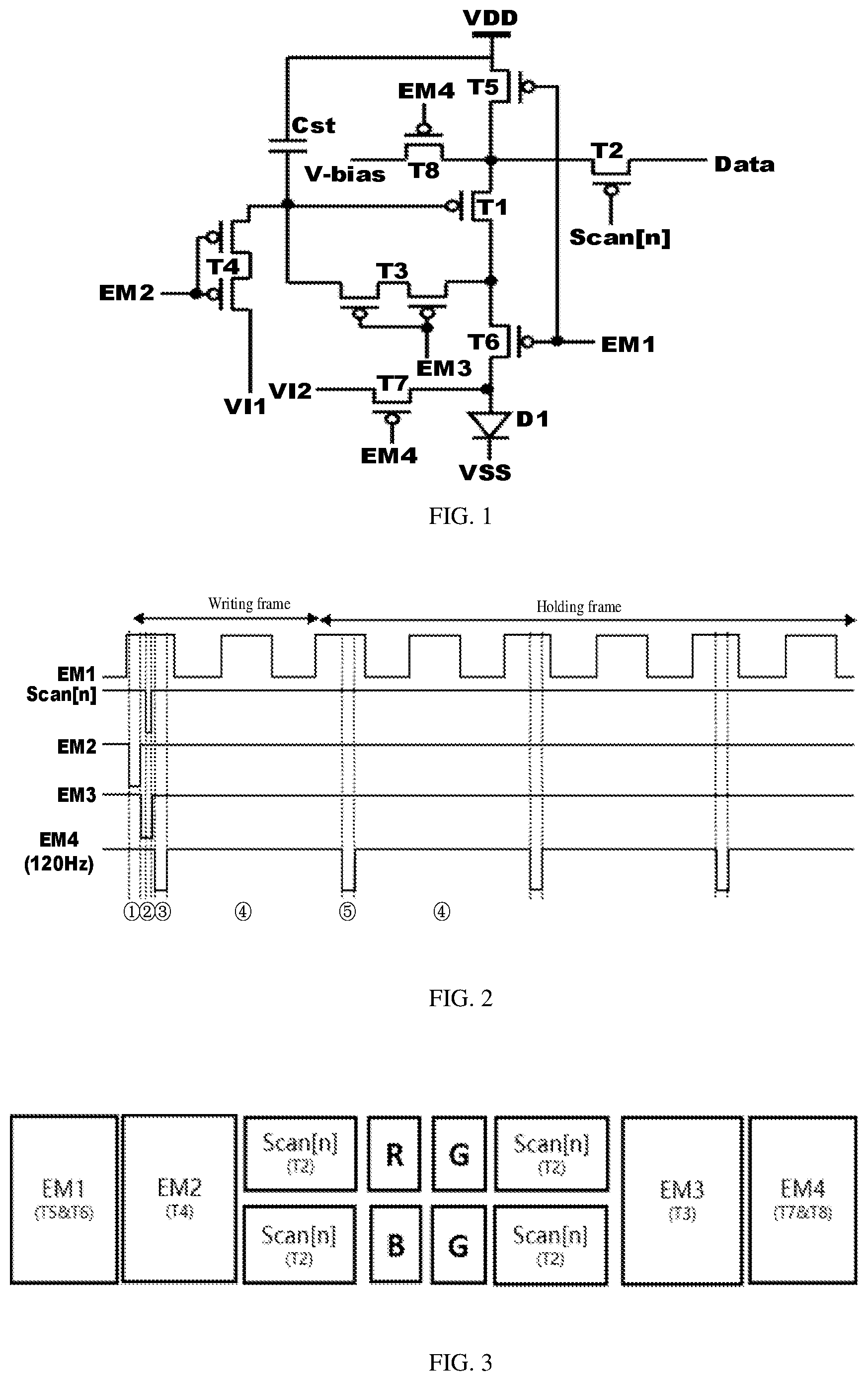
In order to make the objects, technical solutions, and effects of the present disclosure clearer and more explicit, the present disclosure will be described in further detail with reference to the accompanying drawings and embodiments below. It is to be understood that the specific embodiments described herein are merely illustrative of the disclosure and are not intended to limit the disclosure. Furthermore, the terms “first”, “second” are only for the purpose of description, and are not to be construed as indicating or implying relative importance or implicitly indicating the number of indicated technical features, such that the features defined by “first” and “second” may explicitly or implicitly include one or more of the recited features, and in the description of the present disclosure, “a plurality of” means two or more unless expressly and specifically defined otherwise. Referring to to 3 , is a schematic structural diagram of a pixel circuit according to the related art. is a timing diagram of the pixel circuit shown in . Thin film transistors in a self-emitting pixel circuit are mostly single low-temperature polysilicon thin film transistors (LTPS TFT) only or a combination of low-temperature polysilicon thin film transistor and metal oxide thin film transistors (low-temperature polysilicon and oxide, LTPO TFT), so as to drive the light-emitting device D 1 . A common design when driving at a low refresh frequency (40 Hz or less) is to apply a high-frequency bias voltage to a driving transistor T 1 through a second reset transistor T 8 and to reset an anode of a light-emitting device D 1 through a first reset transistor T 7 , so that the flicker at a low frequency may be improved. Specifically, the driving process of the pixel circuit shown in in one frame is shown in . 1). Writing Frame At a stage {circle around ( 1 )}, a control signal EM 1 is at a high level, and a first light-emitting control transistor T 5 and a second light-emitting control transistor T 6 are turned off; a control signal EM 2 is at a low level, a third reset transistor T 4 is turned on, and a second initialization signal VI 1 resets a potential of a gate of the driving transistor T 1 . At a stage {circle around ( 2 )}, a scanning signal Scan [n] is at a low level, and a writing transistor T 2 is turned on; a control signal EM 3 is at a low level, a compensation transistor T 3 is turned on, and a data signal Data is written to the gate of the driving transistor T 1 and a storage capacitor Cst. At a stage {circle around ( 3 )}, a control signal EM 4 is at a low level, the first reset transistor T 7 and a second reset transistor T 8 are turned on, the anode of the light-emitting device D 1 is reset by a first initialization signal VI 2 , and a bias voltage signal V-bias is applied to the source and drain of the driving transistor T 1 for resetting, so that hysteresis of the driving transistor T 1 may be improved, thereby improving the flicker occurring at the low frequency. At a stage {circle around ( 4 )}, the control signal EM 1 is at a low level, the first light-emitting control transistor T 5 and the second light-emitting control transistor T 6 are turned on, and the light-emitting device D 1 emits light. 2). Holding Frame At a step {circle around ( 5 )}, the control signal EM 1 is at the high level, and the first light-emitting control transistor T 5 and the second light-emitting control transistor T 6 are turned off; the control signal EM 4 is at the low level, the first reset transistor T 7 and the second reset transistor T 8 are turned on, and the first initialization signal VI 2 is used to reset the anode of the light-emitting device D 1 , and the bias voltage signal V-bias is applied to the source and drain of the driving transistor T 1 for resetting, so that the hysteresis of the driving transistor T 1 may be improved, thereby improving flicker occurring at the low frequency. It should be noted that the higher the frequency of the control signal EM 4 , the better the effect of improving the flicker. Since the gate of the first reset transistor T 7 and the gate of the second reset transistor T 8 share the control signal EM 4 and are synchronously turned on or turned off, the reset frequency of the anode of the light-emitting device D 1 increases as the frequency of the control signal EM 4 increases, which deteriorates the display uniformity of the pixel circuit or the display panel at a low gray scale and reduces the display quality. The inventors have found that the display uniformity at the low gray scale is strongly related to the charging process of the anode of the light-emitting device D 1 . The operation process of the light-emitting device D 1 at the low gray scale is that the anode of the light-emitting device D 1 is first reset to a low voltage, and then slowly charged to an operating voltage or a turn-on voltage, which affects the display uniformity at the low gray scale. If the reset frequency of the anode of the light-emitting device D 1 is too high, the light-emitting device D 1 is frequently in a reset-charging process, which causes the anode of the light-emitting device D 1 to be undercharged and deteriorates display uniformity at the low gray scale. is a schematic structural diagram of a display panel in which the pixel circuit shown in is located. The display panel includes a pixel circuit for red color (R) light emitting, a pixel circuit for green color (G) light emitting, and a pixel circuit for blue color (B) light emitting in a display area, which may be arranged in the display area in an array. The display panel also includes a plurality of gate driving circuits in a non-display area to provide various signals required for respective pixel circuits. For example, a first gate driving circuit, a second gate driving circuit, a third gate driving circuit, and a fourth gate driving circuit may sequentially provide the control signal EM 1 , the control signal EM 2 , the control signal EM 3 , and the control signal EM 4 to respective pixel circuits, respectively. A fifth gate driving circuit and a sixth gate driving circuit distributed on both sides of the display area may supply the same scanning signal Scan [n] to the same scanning line to improve the driving capability of the scanning signal Scan [n] by double-side driving. In view of the above-mentioned technical problem that the flicker at the low refresh frequency and the uniformity at low gray scale are difficult to be synchronously improved, the present embodiment provides a pixel circuit, referring to to 12 . As shown in , 7 , and 10 , the pixel circuit includes a first light-emitting control transistor T 5 , a driving transistor T 1 , a second light-emitting control transistor T 6 , and a light-emitting device D 1 , and one of a source or a drain of the first light-emitting control transistor T 5 is electrically connected to a first power supply line; one of a source or a drain of the driving transistor T 1 is electrically connected to another of the source or the drain of the first light-emitting control transistor T 5 ; one of a source or a drain of the second light-emitting control transistor T 6 is electrically connected to another of the source or the drain of the driving transistor T 1 ; the anode of the light emitting device D 1 is electrically connected to another of the source or the drain of the second light-emitting control transistor T 6 , and a cathode of the light emitting device D 1 is electrically connected to a second power supply line. The number of times to reset the source or drain of the driving transistor T 1 in one frame is greater than the number of times to reset the anode of the light emitting device D 1 in one frame. It may be understood that the pixel circuit according to the present embodiment may reduce a drift amplitude of a threshold voltage of the driving transistor T 1 by resetting the potential of the source or the drain of the driving transistor T 1 , thereby improving the flicker phenomenon at the low refresh frequency. At the same time, the number of times to reset the source or drain of the driving transistor T 1 in one frame is larger than the number of times to reset the anode of the light-emitting device D 1 in one frame, so that the number of times to reset the anode of the light-emitting device D 1 may be reduced, the number of repetitive charging of the anode of the light-emitting device D 1 may be reduced, and the problem of insufficient charging of the anode potential of the light-emitting device D 1 is improved, thereby improving the uniformity at the low gray scale. It should be noted that a gate of the first light-emitting control transistor T 5 and a gate of the second light-emitting control transistor T 6 may share the same control line for transmitting the control signal EM 1 ; each of the gate of the first light-emitting control transistor T 5 and the gate of the second light-emitting control transistor T 6 may be individually provided with a control line. The first power supply line is used to transmit a positive power supply signal VDD, the second power supply line is used to transmit a negative power supply signal VSS, and a potential of the positive power supply signal VDD is higher than a potential of the negative power supply signal VSS. The light-emitting device D 1 may be an organic light-emitting diode, a micro light-emitting diode, a mini light-emitting diode, or a quantum dot light-emitting diode. In an embodiment, as shown in , the pixel circuit further includes a first reset transistor T 7 and a bias transistor, one of the source or drain of the first reset transistor T 7 is electrically connected to the anode of the light-emitting device D 1 , another of the source or the drain of the first reset transistor T 7 is electrically connected to the first reset line, and a gate of the first reset transistor T 7 is electrically connected to the first control line. One of the source or the drain of the bias transistor is electrically connected to the source or the drain of the driving transistor T 1 , another of the source or the drain of the bias transistor is electrically connected to a first wiring, and a gate of the bias transistor is electrically connected to the second wiring. One frame includes at least one first period and at least one second period. The first reset transistor T 7 and the bias transistor are both turned on during the at least one first period. During the at least one second period, the first reset transistor T 7 is turned off, and the bias transistor is turned on. It may be understood that in the pixel circuit according to the present embodiment, the first reset transistor T 7 and the bias transistor may be controlled separately by different control lines, both the first reset transistor T 7 and the bias transistor may be controlled to be turned on in the first time period, and the first reset transistor T 7 is controlled to be turned off and the bias transistor is controlled to be turned on in a second time period, so that the number of times to reset the source or drain of the driving transistor T 1 in one frame is configured to be greater than the number of times to reset the anode of the light-emitting device D 1 in one frame, the number of times to reset the anode of the light-emitting device D 1 may be reduced, and the number of repetitive charging of the anode of the light-emitting device D 1 may be reduced, thereby improving the problem of insufficient charging of the anode potential of the light-emitting device D 1 , and further improving the uniformity at the low gray scale. It should be noted that the first period may be a stage {circle around ( 3 )} as shown in or , and the second period may be a stage {circle around ( 5 )} as shown in . The first period may be a stage {circle around ( 2 )} or a stage {circle around ( 5 )} as shown in , and the second period may be a stage {circle around ( 4 )} as shown in . In an embodiment, as shown in , the bias transistor is a second reset transistor T 8 , the first wiring is a second reset line, and the second wiring is a second control line. One of the source or drain of the second reset transistor T 8 is electrically connected to the source or drain of the driving transistor T 1 , another of the source or drain of the second reset transistor T 8 is electrically connected to the second reset line, and the gate of the second reset transistor T 8 is electrically connected to the second control line. It should be noted that in , the first reset line is used to transmit the first initialization signal VI 2 . The first control line is used to transmit the control signal EM 4 . The second reset line is used to transmit the bias voltage signal V-bias to reset the source or drain of the driving transistor T 1 . The second control line is used to transmit the control signal EM 5 . It may be appreciated that in the pixel circuit according to the present embodiment, the first reset transistor T 7 and the second reset transistor T 8 may be controlled separately by different control lines, the number of times to reset the source or drain of the driving transistor T 1 in one frame is configured to be greater than the number of times to reset the anode of the light-emitting device D 1 in one frame, the number of times to reset the anode of the light-emitting device D 1 may be reduced, and the number of repetitive charging of the anode of the light-emitting device D 1 may be reduced, thereby improving the problem of insufficient charging of the anode potential of the light-emitting device D 1 , and further improving the uniformity at the low gray scale. In an embodiment, as shown in , 7 , and 10 , the pixel circuit further includes a storage capacitor Cst, one end of which is electrically connected to the gate of the driving transistor T 1 , and another end of which is electrically connected to the first power supply line. In an embodiment, as shown in , 7 , and 10 , the pixel circuit further includes a third reset transistor T 4 , one of a source or a drain of the third reset transistor T 4 is electrically connected to the gate of the driving transistor T 1 , another of the source or the drain of the third reset transistor T 4 is electrically connected to a third reset line, and a gate of the third reset transistor T 4 is electrically connected to the fifth control line. It should be noted that the third reset line is used to transmit the second initialization signal VI 1 . The fifth control line is used to transmit the control signal EM 2 in . The third reset transistor T 4 may be formed by connecting two low-temperature polysilicon thin film transistors in series, so that the dynamic performance may be improved, and the leakage current of the driving transistor T 1 may be reduced. In an embodiment, as shown in , 7 and 10 , the pixel circuit further includes a compensation transistor T 3 , one of a source or a drain of the compensation transistor T 3 is electrically connected to the gate of the driving transistor T 1 , another of the source or the drain of the compensation transistor T 3 is electrically connected to the other of the source or the drain of the driving transistor T 1 , and the gate of the compensation transistor T 3 is electrically connected to a fourth control line. It should be noted that the fourth control line is used to transmit the control signal EM 3 in . The compensation transistor T 3 may be formed by two low-temperature polysilicon thin film transistors in series, so that the dynamic performance may be improved and the leakage current of the driving transistor T 1 may be reduced. In an embodiment, as shown in , the pixel circuit further includes a writing transistor T 2 , one of a source or a drain of the writing transistor T 2 is electrically connected to one of the source or drain of the driving transistor T 1 , another of the source or the drain of the writing transistor T 2 is electrically connected to the data line, and a gate of the writing transistor T 2 is electrically connected to a third control line. It should be noted that the third control line is used to transmit the scanning signal Scan in . The operation process of the pixel circuit shown in in one frame is shown in , which includes the following driving process. 1). Writing Frame At a stage {circle around ( 1 )}, the control signal EM 1 is at a high level, and the first light-emitting control transistor T 5 and the second light-emitting control transistor T 6 are turned off; the control signal EM 2 is at a low level, the third reset transistor T 4 is turned on, and the second initialization signal VI 1 resets the gate of the driving transistor T 1 . At a stage {circle around ( 2 )}, the scanning signal Scan is at a low level, and the writing transistor T 2 is turned on; the control signal EM 3 is at a low level, the compensation transistor T 3 is turned on, and the data signal Data is written to the gate of the driving transistor T 1 and the storage capacitor Cst. At a stage {circle around ( 3 )}, the control signal EM 4 and the control signal EM 5 are both at a low level, and the first reset transistor T 7 and the second reset transistor T 8 are turned on; the first initialization signal VI 2 resets the anode of the light-emitting device D 1 , and the bias voltage signal V-bias is applied to the source and drain of the driving transistor T 1 , thereby improving the hysteresis of the driving transistor T 1 and improving the flicker at the low frequency. At a stage {circle around ( 4 )}, the control signal EM 1 is at a low level, the first light-emitting control transistor T 5 and the second light-emitting control transistor T 6 are turned on, and the light-emitting device D 1 emits light. At a stage {circle around ( 5 )}, the control signal EM 5 is at a low level, the second reset transistor T 8 is turned on, and the bias voltage signal V-bias resets the source and drain of the driving transistor T 1 . 2). Holding Frame The stage {circle around ( 3 )}, the stage {circle around ( 4 )}, and the stage {circle around ( 5 )} are repeatedly written in the frame. Specifically, the frequency of the control signal EM 5 may be two times as large as the frequency of the control signal EM 4 . For example, the frequency of the control signal EM 5 may be 240 Hz, and the frequency of the control signal EM 4 may be 120 Hz. is a schematic structural diagram of a display panel in which the pixel circuit shown in is located. The display panel includes a pixel circuit for red color (R) light emitting, a pixel circuit for green color (G) light emitting, and a pixel circuit for blue color (B) light emitting in a display area, which may be arranged in the display area in an array. The display panel also includes a plurality of gate driving circuits in a non-display area to provide various signals required for respective pixel circuits. For example, a first gate driving circuit, a second gate driving circuit, a third gate driving circuit, a fourth gate driving circuit, and a fifth gate driving circuit may sequentially supply the control signal EM 1 , the control signal EM 2 , the control signal EM 3 , the control signal EM 4 , and the control signal EM 5 to respective pixel circuits, respectively. A sixth gate driving circuit and a seventh gate driving circuit distributed on both sides of the display area may supply the same scanning signal Scan to the same scanning line to improve the driving capability of the scanning signal Scan by double-side driving. In comparison with the pixel circuit shown in , in , a gate of a writing transistor T 2 and a gate of a compensation transistor T 3 share the same third control line. A first control line is used to transmit a control signal EM 2 . A second control line is used to transmit a control signal EM 3 . The third control line is used to transmit the scanning signal Scan [n]. A fifth control line is used to transmit the scanning signal Scan [n−1]. The operation process of the pixel circuit shown in in one frame is shown in , which includes the following driving process. 1). Writing Frame At a stage {circle around ( 1 )}, the control signal EM 1 is at a high level, and the first light-emitting control transistor T 5 and the second light-emitting control transistor T 6 are turned off; the scanning signal Scan [n−1] is at a low level, the third reset transistor T 4 is turned on, and the second initialization signal VI 1 resets the gate of the driving transistor T 1 . At a stage {circle around ( 2 )}, the scanning signal Scan [n] is at a low level, the writing transistor T 2 and the compensation transistor T 3 are turned on, and the data signal Data is written to the gate of the driving transistor T 1 and the storage capacitor Cst. At a stage {circle around ( 3 )}, the control signal EM 2 and the control signal EM 3 are both at a low level, and the first reset transistor T 7 and the second reset transistor T 8 are turned on; the first initialization signal VI 2 resets the anode of the light-emitting device D 1 , and the bias voltage signal V-bias is applied to the source and drain of the driving transistor T 1 , thereby improving the hysteresis of the driving transistor T 1 and improving the flicker at the low frequency. At a stage {circle around ( 4 )}, the control signal EM 1 is at a low level, the first light-emitting control transistor T 5 and the second light-emitting control transistor T 6 are turned on, and the light-emitting device D 1 emits light. At a stage {circle around ( 5 )}, the control signal EM 3 is at a low level, the second reset transistor T 8 is turned on, and the bias voltage signal V-bias resets the source and drain of the driving transistor T 1 . 2k). Holding Frame The stage {circle around ( 3 )}, the stage {circle around ( 4 )}, and the stage {circle around ( 5 )} are repeatedly written in the frame. Specifically, the frequency of the control signal EM 3 may be two times as large as the frequency of the control signal EM 2 . For example, the frequency of the control signal EM 3 may be 240 Hz, and the frequency of the control signal EM 2 may be 120 Hz. is a schematic structural diagram of a display panel in which the pixel circuit shown in is located. The display panel includes a pixel circuit for red color (R) light emitting, a pixel circuit for green color (G) light emitting, and a pixel circuit for blue color (B) light emitting in a display area, which may be arranged in the display area in an array. The display panel also includes a plurality of gate driving circuits in a non-display area to provide various signals required for respective pixel circuits. For example, a first gate driving circuit, a second gate driving circuit, and a third gate driving circuit may sequentially supply the control signal EM 1 , the control signal EM 2 , and the control signal EM 3 to respective pixel circuits, respectively. Fourth gate driving circuits and fifth gate driving circuits distributed on both sides of the display area may supply the same scanning signal Scan [n] to the same scanning line and supply the same scanning signal Scan [n−1] to the same scanning line, so as to improve the driving capability of the two scanning signals by double-side driving. It may be appreciated that since the scan signal Scan [n] and the scan signal Scan [n−1] may be provided through the fourth gate driving circuit and the fifth gate driving circuit without other gate driving circuits, the number of gate driving circuits is reduced, facilitating the implementation of narrower bezel. At the same time, since the gate of the compensation transistor T 3 and the gate of the writing transistor T 2 share the same third control line, the number of wirings in the display area or the area of the wirings is reduced, and it is advantageous to increase the density of the pixel circuits or the aperture rate of the display panel. In an embodiment, referring to to 9 , the number of times the second reset transistor T 8 is turned on in one frame is greater than the number of times the first reset transistor T 7 is turned on in one frame. It should be noted that in the present embodiment, the anode of the light-emitting device D 1 may be reset once every time the first reset transistor T 7 is turned on, and the source and/or drain of the driving transistor T 1 may be reset once every time the second reset transistor T 8 is turned on. In an embodiment, one frame includes a writing frame and a holding frame, the number of times the second reset transistor T 8 is turned on in the writing frame is greater than the number of times the first reset transistor T 7 is turned on in the writing frame, and the number of times the second reset transistor T 8 is turned on in the holding frame is greater than the number of times the first reset transistor T 7 is turned on in the holding frame. It should be noted that in the present embodiment, the number of times the first reset transistor T 7 is turned on is configured to be less in the holding frame, so that the number of times to reset the anode of the light-emitting device D 1 may be reduced, and the number of charges and discharges of the anode of the light-emitting device D 1 may be reduced, thereby facilitating improvement of display uniformity at the low gray scale. In an embodiment, the first control line is used to transmit a first control signal and the second control line is used to transmit a second control signal, the number of pulses of the second control signal in one frame is greater than the number of pulses of the first control signal in one frame. It should be noted that in the present embodiment, the first control signal may be the control signal EM 4 in to 6 or the control signal EM 2 in to 9 . The second control signal may be the control signal EM 5 in to 6 or the control signal EM 3 in to 9 . In an embodiment, one frame includes a writing frame and a holding frame, the number of pulses in the writing frame of the second control signal is greater than the number of pulses in the writing frame of the first control signal, and the number of pulses in the holding frame of the second control signal is greater than the number of pulses in the holding frame of the first control signal. It should be noted that each pulse of the first control signal may turn on the first reset transistor T 7 once to reset the anode potential of the light-emitting device D 1 . Each pulse of the second control signal may turn on the second reset transistor T 8 once to reset the source or the drain of the driving transistor T 1 . In an embodiment, referring to to 12 , as shown in , a bias transistor is a writing transistor T 2 , a first wiring is a data line, and a second wiring is a third control line; one of a source or a drain of the writing transistor T 2 is electrically connected to a source or a drain of the driving transistor T 1 , another of the source or the drain of the writing transistor T 2 is electrically connected to the data line, and a gate of the writing transistor T 2 is electrically connected to the third control line; the number of times the writing transistor T 2 is turned on in one frame is greater than the number of times the first reset transistor T 7 is turned on in one frame. It should be noted that, it may be understood that in the pixel circuit according to the present embodiment, by individually controlling the first reset transistor T 7 and the writing transistor T 2 , the number of times to reset the source or drain of the driving transistor T 1 in one frame is configured to be larger than the number of times to reset the anode of the light-emitting device D 1 in one frame, the number of times to reset the anode of the light-emitting device D 1 may be reduced, and the number of repetitive charging of the anode of the light-emitting device D 1 may be reduced, thereby improving the problem of insufficient charging of the anode potential of the light-emitting device D 1 , and further improving the uniformity at the low gray scale. In addition, in the present embodiment, the writing transistor T 2 is multiplexed to reset the source and/or the drain of the driving transistor T 1 , so that not only the number of transistors required by the pixel circuit is reduced, but also the area occupied by the pixel circuit may be reduced, thereby increasing the density of the pixel circuit in the display area. In comparison with the pixel circuit shown in , in , the first control line is used to transmit the control signal EM 4 . The third control line is used to transmit the scanning signal Scan. The fourth control line is used to transmit the control signal EM 3 . The fifth control line is used to transmit the control signal EM 2 . The operation process of the pixel circuit shown in in one frame is shown in , which includes the following driving process. 1). Writing Frame At a stage {circle around ( 1 )}, the control signal EM 1 is at a high level, and the first light-emitting control transistor T 5 and the second light-emitting control transistor T 6 are turned off; the control signal EM 2 is at a low level, the third reset transistor T 4 is turned on, and the second initialization signal VI 1 resets the gate of the driving transistor T 1 . At a stage {circle around ( 2 )}, the control signal EM 4 is at a low level, the first reset transistor T 7 is turned on, and the first initialization signal VI 2 resets the anode of the light-emitting device D 1 ; the scanning signal Scan is at a low level, the writing transistor T 2 is turned on, the control signal EM 3 is at a low level, the compensation transistor T 3 is turned on, and the data signal Data is written to the gate of the driving transistor T 1 and the storage capacitor Cst. At a stage {circle around ( 3 )}, the control signal EM 1 is at a low level, the first light-emitting control transistor T 5 and the second light-emitting control transistor T 6 are turned on, and the light-emitting device D 1 emits light. At a stage {circle around ( 4 )}, the control signal EM 1 is at a high level, and the first light-emitting control transistor T 5 and the second light-emitting control transistor T 6 are turned off; the scanning signal Scan is at a low level, the second reset transistor T 8 is turned on, and the bias voltage signal V-bias resets the source and drain of the driving transistor T 1 . At a stage {circle around ( 5 )}, the control signal EM 4 is at a low level, the first reset transistor T 7 is turned on, and the first initialization signal VI 2 resets the anode of the light-emitting device D 1 ; the scanning signal Scan is at a low level, the second reset transistor T 8 is turned on, and the bias voltage signal V-bias resets the source and drain of the driving transistor T 1 . 2). Holding Frame The stage {circle around ( 3 )}, the stage {circle around ( 4 )}, and the stage {circle around ( 5 )} are repeatedly written in the frame. Specifically, the frequency of the scanning signal Scan may be two times as large as the frequency of the control signal EM 4 . For example, the frequency of the scanning signal Scan may be 240 Hz, and the frequency of the control signal EM 4 may be 120 Hz. is a schematic structural diagram of a display panel in which the pixel circuit shown in is located. The display panel includes a pixel circuit for red color (R) light emitting, a pixel circuit for green color (G) light emitting, and a pixel circuit for blue color (B) light emitting in a display area, which may be arranged in the display area in an array. The display panel also includes a plurality of gate driving circuits in a non-display area to provide various signals required for respective pixel circuits. For example, a first gate driving circuit, a second gate driving circuit, a third gate driving circuit, and a fourth gate driving circuit may sequentially supply the control signal EM 1 , the control signal EM 2 , the control signal EM 3 , and the control signal EM 4 to respective pixel circuits, respectively. A fifth gate driving circuit and a sixth gate driving circuit distributed on both sides of the display area may supply the same scanning signal Scan to the same scanning line to improve the driving ability of the two scanning signals by double-side driving. In an embodiment, referring to to 12 , one frame includes a writing frame and a holding frame, the number of times the writing transistor T 2 is turned on in the writing frame is greater than the number of times the first reset transistor T 7 is turned on in the writing frame, and the number of times the writing transistor T 2 is turned on in the holding frame is greater than the number of times the first reset transistor T 7 is turned on in the holding frame. It should be noted that a first turn-on of the writing transistor T 2 in the writing frame is to write the data signal Data to the gate of the driving transistor T 1 , and a second turn-on of the writing transistor T 2 in the writing frame is to reset the source and drain of the driving transistor T 1 using the low potential of the data signal Data. Each turn-on of the writing transistor T 2 in the holding frame is to reset the source and drain of the driving transistor T 1 . In an embodiment, the first control line is used to transmit a first control signal, the third control line is used to transmit a third control signal, the number of pulses of the third control signal in one frame is greater than the number of pulses of the first control signal in one frame. It should be noted that as shown in to 12 , the first control signal may be the control signal EM 4 . The third control signal may be the scanning signal Scan. In an embodiment, the data line is used to transmit a data signal Data, the number of pulses of the third control signal in the writing frame is greater than the number of pulses of the first control signal in the writing frame, and the data signal Data has at least one pulse in the writing frame; the number of pulses of the third control signal in the holding frame is greater than the number of pulses of the first control signal in the holding frame, and the number of pulses of the data signal Data in the holding frame is zero. It should be noted that in the present embodiment, each of the pulses of the first control signal may turn on the first reset transistor T 7 once, and each of the pulses of the third control signal may turn on the writing transistor T 2 once. It should be noted that at least one of the first reset transistor T 7 , the second reset transistor T 8 , the third reset transistor T 4 , the compensation transistor T 3 , the writing transistor T 2 , the driving transistor T 1 , the first light-emitting control transistor T 5 , and the second light-emitting control transistor T 6 may be a low-temperature polysilicon thin film transistor, and/or may be an oxide thin film transistor. In an embodiment, the present embodiment provides a display panel including a plurality of pixel circuits in at least one of the above-described embodiments and at least two gate driving circuits, one of the gate driving circuits outputs a first driving signal to control the source or drain of the driving transistor T 1 to reset, and another of the gate driving circuits outputs a second driving signal to control the anode of the light-emitting device D 1 to reset; a frequency of the first driving signal is higher than that of the second driving signal. It may be appreciated that since the display panel provided in this embodiment includes a plurality of pixel circuits in at least one of the above-described embodiments, it is also possible to reduce the drift amplitude of the threshold voltage of the driving transistor T 1 by resetting the potential of the source or the drain of the driving transistor T 1 , thereby improving the flicker phenomenon at the low refresh frequency. At the same time, the number of times to reset the source or drain of the driving transistor T 1 in one frame is larger than the number of times to reset the anode of the light-emitting device D 1 in one frame, so that the number of times to reset the anode of the light-emitting device D 1 may be reduced, the number of repetitive charging of the anode of the light-emitting device D 1 may be reduced, and the problem of insufficient charging of the anode potential of the light-emitting device D 1 is improved, thereby improving the uniformity at the low gray scale. It should be noted that the first driving signal may be the control signal EM 5 in , and the second driving signal may be the control signal EM 4 in , 5 and 6 ; alternatively, the first driving signal may be the control signal EM 3 in , and the second driving signal may be the control signal EM 2 in , 8 and 9 ; alternatively, the first driving signal may be the scanning signal Scan in , 11 , and 12 , and the second driving signal may be the control signal EM 4 in , 11 , and 12 . It may be understood that, for those ordinary skilled in the art, equivalent replacements or changes may be made according to the technical solutions and inventive concepts of the present disclosure, and all such changes or replacements should fall within the protection scope of the claims appended to the present disclosure.
Figures (4)
Citations
This patent cites (18)
- US2017/0243542
- US2018/0130420
- US2021/0407383
- US2021/0407386
- US2022/0366830
- US108564920
- US111754922
- US113012643
- US114758617
- US114758618
- US114974130
- US115148144
- US115410523
- US115602107
- US115662328
- US115662356
- US20210055146
- US2023011474