Monitoring Circuit, Semiconductor Integrated Circuit Device, and Vehicle
Abstract
A monitoring circuit includes first and second oscillators, first and second frequency dividers, first and second counters, a determination portion, and an identification portion. The first and second frequency dividers respectively divide frequencies of first and second clock signals outputted from the first and second oscillators, respectively. The first and second counters respectively count the numbers of clocks of the second and first clock signals at first and second numbers of periods of first and second frequency-divided signals outputted from the first and second frequency dividers, respectively. The determination portion determines, based on results of counting by the first and second counters, whether or not an abnormality has occurred in either of the first and second clock signals. The identification portion identifies, at the occurrence of an abnormality in either of the first and second clock signals, which of the first and second clock signals is in an abnormal state.
Claims (10)
1 . A monitoring circuit, comprising: a first oscillator configured to output a first clock signal; a second oscillator configured to output a second clock signal; a first frequency divider configured to divide a frequency of the first clock signal; a second frequency divider configured to divide a frequency of the second clock signal; a first counter configured to count a number of clocks of the second clock signal at a first number of periods of a first frequency-divided signal outputted from the first frequency divider; a second counter configured to count a number of clocks of the first clock signal at a second number of periods of a second frequency-divided signal outputted from the second frequency divider; a determination portion configured to determine, based on results of counting by the first counter and the second counter, whether or not an abnormality has occurred in either of the first clock signal and the second clock signal; and an identification portion configured to identify, at an occurrence of an abnormality in either of the first clock signal and the second clock signal, which of the first clock signal and the second clock signal is in an abnormal state.
Show 9 dependent claims
2 . The monitoring circuit according to claim 1 , wherein the identification portion includes: a third oscillator configured to output a third clock signal; and a third counter configured to count a number of clocks of the third clock signal at a third number of periods of the second frequency-divided signal or a fourth number of periods of the first frequency-divided signal, and the identification portion is configured to identify, based on results of counting by the first counter, the second counter, and the third counter, at the occurrence of an abnormality in either of the first clock signal and the second clock signal, which of the first clock signal and the second clock signal is in the abnormal state.
3 . The monitoring circuit according to claim 2 , wherein the first oscillator is configured to oscillate based on a first reference voltage supplied from a first reference voltage source, and the second oscillator is configured to oscillate based on a second reference voltage supplied from a second reference voltage source.
4 . The monitoring circuit according to claim 3 , wherein the third counter is configured to count the number of clocks of the third clock signal at the third number of periods of the second frequency-divided signal, and the third oscillator is configured to oscillate based on the first reference voltage, or the third counter is configured to count the number of clocks of the third clock signal at the fourth number of periods of the first frequency-divided signal, and the third oscillator is configured to oscillate based on the second reference voltage.
5 . The monitoring circuit according to claim 1 , wherein the identification portion includes at least one of a first charging and discharging circuit configured to perform charging and discharging based on the first clock signal and a second charging and discharging circuit configured to perform charging and discharging based on the second clock signal, and the identification portion is configured to identify, based on an output of at least one of the first charging and discharging circuit and the second charging and discharging circuit, at the occurrence of an abnormality in either of the first clock signal and the second clock signal, which of the first clock signal and the second clock signal is in the abnormal state.
6 . The monitoring circuit according to claim 5 , wherein the first oscillator is configured to oscillate based on a first reference voltage supplied from a first reference voltage source, and the second oscillator is configured to oscillate based on a second reference voltage supplied from a second reference voltage source.
7 . The monitoring circuit according to claim 1 , further comprising: a selector configured to select either one of the first clock signal and the second clock signal.
8 . The monitoring circuit according to claim 7 , wherein upon determination by the determination portion that an abnormality has occurred in either of the first clock signal and the second clock signal, based on a result of identification by the identification portion, the selector selects a normal-state clock signal from the first clock signal and the second clock signal.
9 . A semiconductor integrated circuit device comprising the monitoring circuit according to claim 1 .
10 . A vehicle comprising the monitoring circuit according to claim 1 .
Full Description
Show full text →
CROSS-REFERENCE TO RELATED APPLICATIONS
This application is a continuation under 35 U.S.C. § 120 of No. PCT/JP2022/045459 filed on Dec. 9, 2022, which is incorporated herein by reference, and which claimed priority to Japanese Patent Application No. 2022-030980 filed in Japan on Mar. 1, 2022. The present application likewise claims priority under 35 U.S.C. § 119 to Japanese Application No. 2022-030980 filed in Japan on Mar. 1, 2022, the entire content of which is also incorporated herein by reference, the entire contents of which are hereby incorporated by reference.
BACKGROUND OF THE INVENTION
1. Technical Field The disclosure herein relates to a monitoring circuit and to a semiconductor integrated circuit device and a vehicle each including the monitoring circuit. 2. Description of Related Art In the field of in-vehicle devices, it has been demanded to monitor an operation state of an IC (Integrated Circuit) and to perform, at the occurrence of an abnormality, a protective operation against the abnormality. Furthermore, particularly in products requested to achieve a level of functional safety standardized by ISO 26262 and so on, it is desired not only to simply perform the protective operation at the occurrence of an abnormality but also to maintain an operation even at the occurrence of an abnormality. As a circuit that performs abnormality monitoring, generally used is a circuit that operates based on a clock signal outputted from an oscillator. Accordingly, in a case of an abnormal stop of the oscillator, it is no longer possible to perform the abnormality monitoring and thus to perform the protective operation or maintain an operation. It is, therefore, extremely crucial to maintain an operation of the oscillator.
BRIEF DESCRIPTION OF THE DRAWINGS
is a view showing a configuration of a monitoring circuit according to a first embodiment. is a view showing a relationship between a frequency-divided signal and a clock signal. is a view showing combinational logic of a combinational circuit in the first embodiment. is a view showing a configuration of a monitoring circuit according to a second embodiment. is a view showing combinational logic of a combinational circuit in the second embodiment. is a view showing a configuration example of a first charging and discharging circuit. is a waveform diagram of a ramp voltage. is a view showing schematic configurations of semiconductor integrated circuit devices. is an external appearance view of a vehicle. is a view showing a configuration of a monitoring circuit according to a modification example.
DESCRIPTION OF EMBODIMENTS
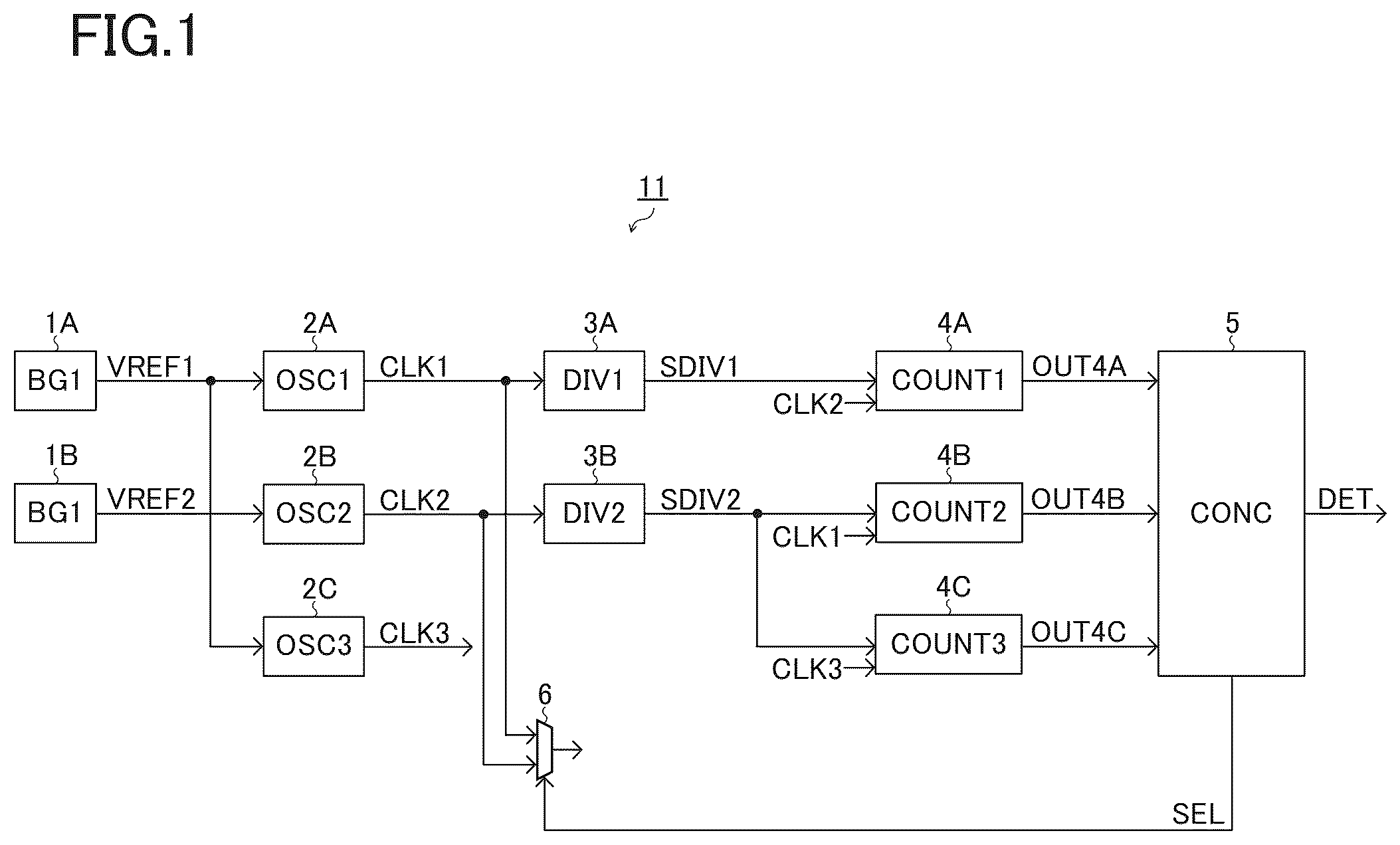
In the present description, a reference voltage refers to a voltage that is constant in an ideal state and is practically a voltage that may slightly vary depending on a temperature change or the like. In the present description, a constant current refers to a current that is constant in an ideal state and is practically a current that may slightly vary depending on a temperature change or the like. First Embodiment is a view showing a configuration of a monitoring circuit 11 according to a first embodiment (hereinafter, referred to as a monitoring circuit 11 ). The monitoring circuit 11 includes first and second reference voltage sources 1 A and 1 B, first to third oscillators 2 A to 2 C, first and second frequency dividers 3 A and 3 B, first to third counters 4 A to 4 C, a combinational circuit 5 , and a selector 6 . The first reference voltage source 1 A generates a first reference voltage VREF 1 . While this embodiment uses a bandgap reference circuit as the first reference voltage source 1 A, any other type of reference voltage source than the bandgap reference circuit may be used as the first reference voltage source 1 A. The first reference voltage VREF 1 is supplied to each of the first oscillator 2 A and the third oscillator 2 C. The second reference voltage source 1 B generates a second reference voltage VREF 2 . While this embodiment uses a bandgap reference circuit as the second reference voltage source 1 B, any other type of reference voltage source than the bandgap reference circuit may be used as the second reference voltage source 1 B. The second reference voltage VREF 2 is supplied to the second oscillator 2 B. A set value of the second reference voltage VREF 2 may be equal to or different from a set value of the first reference voltage VREF 1 . The first oscillator 2 A operates upon receipt of supply of the first reference voltage VREF 1 and generates a first clock signal CLK 1 . The first oscillator 2 A outputs the first clock signal CLK 1 . The second oscillator 2 B operates upon receipt of supply of the second reference voltage VREF 2 and generates a second clock signal CLK 2 . The second oscillator 2 B outputs the second clock signal CLK 2 . The third oscillator 2 C operates upon receipt of supply of the first reference voltage VREF 1 and generates a third clock signal CLK 3 . The third oscillator 2 C outputs the third clock signal CLK 3 . A set frequency of the first clock signal CLK 1 is equal to a set frequency of the second clock signal CLK 2 . A set frequency of the third clock signal CLK 3 may be equal to or different from each of the set frequency of the first clock signal CLK 1 and the set frequency of the second clock signal CLK 2 . In the following description, it is assumed that the set frequency of the third clock signal CLK 3 is equal to each of the set frequency of the first clock signal CLK 1 and the set frequency of the second clock signal CLK 2 . The first frequency divider 3 A divides a frequency of the first clock signal CLK 1 so as to generate a first frequency-divided signal SDIV 1 . The first frequency divider 3 A outputs the first frequency-divided signal SDIV 1 . The second frequency divider 3 B divides a frequency of the second clock signal CLK 2 so as to generate a second frequency-divided signal SDIV 2 . The second frequency divider 3 B outputs the second frequency-divided signal SDIV 2 . The first counter 4 A counts the number of clocks of the second clock signal CLK 2 at a first number of periods of the first frequency-divided signal SDIV 1 . While the first number of periods is one period in this embodiment, the first number of periods may be, for example, a half period, two periods, or three periods. Furthermore, this embodiment assumes that the first frequency divider 3 A divides a frequency by five. Accordingly, in a case where the first clock signal CLK 1 and the second clock signal CLK 2 are in usual states, the first counter 4 A has a number of counts of ten. In consideration of various types of existing errors, for example, when the first counter 4 A has a number of counts not less than nine and not more than 11, the first clock signal CLK 1 and the second clock signal CLK 2 may be regarded as being in the usual states. The second counter 4 B counts the number of clocks of the first clock signal CLK 1 at a second number of periods of the second frequency-divided signal SDIV 2 . While the second number of periods is one period in this embodiment, the second number of periods may be, for example, a half period, two periods, or three periods. Furthermore, this embodiment assumes that the second frequency divider 3 B divides a frequency by five. Accordingly, in the case where the first clock signal CLK 1 and the second clock signal CLK 2 are in the usual states, the second counter 4 B has a number of counts of ten. In consideration of various types of existing errors, for example, when the second counter 4 B has a number of counts not less than nine and not more than 11, the first clock signal CLK 1 and the second clock signal CLK 2 may be regarded as being in the usual states. The third counter 4 C counts the number of clocks of the third clock signal CLK 3 at a third number of periods of the second frequency-divided signal SDIV 2 . While the third number of periods is one period in this embodiment, the third number of periods may be, for example, a half period, two periods, or three periods. Furthermore, this embodiment assumes that the second frequency divider 3 B divides a frequency by five. Accordingly, in a case where the second clock signal CLK 2 and the third clock signal CLK 3 are in usual states, the third counter 4 C has a number of counts of ten. In consideration of various types of existing errors, for example, when the third counter 4 C has a number of counts not less than nine and not more than 11, the second clock signal CLK 2 and the third clock signal CLK 3 may be regarded as being in the usual states. is a view showing a relationship between a frequency-divided signal SDIV and a clock signal CLK supplied to each of the first to third counters 4 A to 4 C. In a case where the frequency-divided signal SDIV and the clock signal CLK are in usual states, each of the counters outputs a low-level signal. In a case where the frequency-divided signal SDIV has a frequency higher than usual and the clock signal CLK is in the usual state, each of the counters has a number of counts smaller than usual and outputs a high-level signal. In a case where the frequency-divided signal SDIV has a frequency lower than usual and the clock signal CLK is in the usual state, each of the counters has a number of counts larger than usual and outputs a high-level signal. In a case where the frequency-divided signal SDIV is fixed to a low level and the clock signal CLK is in the usual state, each of the counters has a number of counts of 0 and outputs a high-level signal. In a case where the frequency-divided signal SDIV is fixed to a high level and the clock signal CLK is in the usual state, each of the counters has a number of counts of 0 and outputs a high-level signal. In a case where the frequency-divided signal SDIV is in the usual state and the clock signal CLK has a frequency higher than usual, each of the counters has a number of counts larger than usual and outputs a high-level signal. In a case where the frequency-divided signal SDIV is in the usual state and the clock signal CLK has a frequency lower than usual, each of the counters has a number of counts smaller than usual and outputs a high-level signal. In a case where the frequency-divided signal SDIV is in the usual state and the clock signal CLK is fixed to a low level, each of the counters has a number of counts of 0 and outputs a high-level signal. In a case where the frequency-divided signal SDIV is in the usual state and the clock signal CLK is fixed to a high level, each of the counters has a number of counts of 0 and outputs a high-level signal. Referring back to , a further description is given of the configuration of the monitoring circuit 11 . The combinational circuit 5 receives an output OUT 4 A of the first counter 4 A, an output OUT 4 B of the second counter 4 B, and an output OUT 4 C of the third counter 4 C. is a view showing combinational logic of the combinational circuit 5 . When at least one of the output OUT 4 A of the first counter 4 A, the output OUT 4 B of the second counter 4 B, and the output OUT 4 C of the third counter 4 C is at a high level, the combinational circuit 5 sets a detection result DET to a high level. That is, the detection result DET at the high level indicates that an abnormality has occurred in at least one of the first to third clock signals CLK 1 to CLK 3 . Furthermore, the detection result DET at a low level indicates that no abnormality has occurred in the first to third clock signals CLK 1 to CLK 3 . In a case where the output OUT 4 A of the first counter 4 A and the output OUT 4 B of the second counter 4 B are both at the high level, the combinational circuit 5 determines that an abnormality has occurred in either of the first clock signal CLK 1 and the second clock signal CLK 2 . Furthermore, in a case where an abnormality has occurred in either of the first clock signal CLK 1 and the second clock signal CLK 2 , when the output OUT 4 C of the third counter 4 C is at a low level, the combinational circuit 5 identifies that the second clock signal CLK 2 and the third clock signal CLK 3 are in normal states and the first clock signal CLK 1 is in an abnormal state. Then, the combinational circuit 5 outputs, as a selection signal SEL, a signal for causing the selector 6 to output the second clock signal CLK 2 . On the other hand, in the case where an abnormality has occurred in either of the first clock signal CLK 1 and the second clock signal CLK 2 , when the output OUT 4 C of the third counter 4 C is at the high level, the combinational circuit 5 identifies that the second clock signal CLK 2 is in the abnormal state. Then, the combinational circuit 5 outputs, as the selection signal SEL, a signal for causing the selector 6 to output the first clock signal CLK 1 . Based on the selection signal SEL outputted from the combinational circuit 5 , the selector 6 selects either one of the first clock signal CLK 1 and the second clock signal CLK 2 . The selection signal SEL outputted from the combinational circuit 5 is a signal based on a result of identification by the combinational circuit 5 . Accordingly, based on a result of identification by the combinational circuit 5 , the selector 6 selects either one of the first clock signal CLK 1 and the second clock signal CLK 2 . To be more specific, based on a result of identification by the combinational circuit 5 , the selector 6 selects a normal-state clock signal from the first clock signal CLK 1 and the second clock signal CLK 2 . This makes it possible to continuously use a normal-state clock signal even at the occurrence of an abnormality in either one of the first clock signal CLK 1 and the second clock signal CLK 2 . While this embodiment has a configuration in which the selection signal SEL is directly supplied to the selector 6 , for example, a microcomputer may receive the selection signal SEL so as to control the selector 6 based on the selection signal SEL. The monitoring circuit 11 does not require provision of a charging and discharging circuit and thus can be reduced in circuit scale. Furthermore, the monitoring circuit 11 uses separate reference voltage sources for the first oscillator 2 A and the second oscillator 2 B, and thus the reference voltage sources each would not constitute a cause of failure common to the first oscillator 2 A and the second oscillator 2 B. This enhances an abnormality detection capability of the monitoring circuit 11 . Furthermore, in the monitoring circuit 11 , one of the reference voltage sources may constitute a cause of failure common to the first oscillator 2 A and the third oscillator 2 C, and one of the frequency dividers may constitute a cause of failure common to the second counter 4 B and the third counter 4 C. Nesting the common causes of failure in this manner further enhances the abnormality detection capability of the monitoring circuit 11 . Second Embodiment is a view showing a configuration of a monitoring circuit 12 according to a second embodiment (hereinafter, referred to as a monitoring circuit 12 ). In , like reference signs denote like parts as in , which, therefore, will not be described in detail. The monitoring circuit 12 has a configuration obtained by excluding the third counter 4 C from the monitoring circuit 11 and additionally including a first charging and discharging circuit 7 A, a second charging and discharging circuit 7 B, and an OR gate 8 . Furthermore, combinational logic of a combinational circuit 5 in this embodiment is different from the combinational logic of the combinational circuit 5 in the first embodiment. is a view showing the combinational logic of the combinational circuit 5 in the second embodiment. The first charging and discharging circuit 7 A performs charging and discharging based on a first clock signal CLK 1 . The second charging and discharging circuit 7 B performs charging and discharging based on a second clock signal CLK 2 . When at least one of respective outputs of a first counter 4 A, a second counter 4 B, the first charging and discharging circuit 7 A, and the second charging and discharging circuit 7 B is a signal indicating detection of an abnormality, the OR gate 8 sets to a high level a detection result DET as an output signal of the OR gate 8 . is a view showing a configuration example of the first charging and discharging circuit 7 A. The first charging and discharging circuit 7 A according to the configuration example shown in includes a constant current source 71 , a capacitor 72 , a MOSFET 73 , hysteresis comparators 74 and 75 , and an OR gate 76 . A power supply voltage VCC is applied to one end of the constant current source 71 . The other end of the constant current source 71 is connected to one end of the capacitor 72 . The other end of the capacitor 72 is connected to a ground potential. The MOSFET 73 is connected in parallel to the capacitor 72 . When the MOSFET 73 is in an off state, the capacitor 72 is charged with a constant current outputted from the constant current source 71 . When the MOSFET 73 is in an on state, the capacitor 72 performs discharging. One continuous off time of the MOSFET 73 is equal in length to one period of the first clock signal CLK 1 . The MOSFET 73 is turned on, for example, in synchronization with a rising edge of the first clock signal CLK 1 . With this configuration, a ramp voltage VRMP having a waveform shown in is generated at a connection node between the constant current source 71 and the capacitor 72 . When the ramp voltage VRMP exceeds a second threshold voltage VTH 2 , the hysteresis comparator 74 outputs a high-level signal. In a case where the first clock signal CLK 1 has a frequency lower than usual, an output signal of the hysteresis comparator 74 is at a high level. Two comparators may be used in place of the hysteresis comparator 74 . When the ramp voltage VRMP becomes smaller than a first threshold voltage VTH 1 (<VTH 2 ), the hysteresis comparator 75 outputs a high-level signal. In a case where the first clock signal CLK 1 has a frequency higher than usual, an output signal of the hysteresis comparator 75 is at a high level. Two comparators may be used in place of the hysteresis comparator 75 . The OR gate 76 outputs a logical sum of an output of the hysteresis comparator 74 and an output of the hysteresis comparator 75 . An output of the OR gate 76 is outputted as the output of the first charging and discharging circuit 7 A. Accordingly, in a case where the first clock signal CLK 1 is in an abnormal state, the output of the first charging and discharging circuit 7 A is at a high level. A configuration example of the second charging and discharging circuit 7 B is similar to the configuration example of the first charging and discharging circuit 7 A. In the second charging and discharging circuit 7 B, however, the MOSFET 73 is turned on/off based not on the first clock signal CLK 1 but on the second clock signal CLK 2 . The first charging and discharging circuit 7 A and the second charging and discharging circuit 7 B may be configured differently from each other. There may be adopted a configuration in which, unlike in this embodiment, the second charging and discharging circuit 7 B is not provided. There may also be adopted a configuration in which the first charging and discharging circuit 7 A is not provided, and the output of the second charging and discharging circuit 7 B is supplied to the combinational circuit 5 . Application Example, Etc. is a view showing schematic configurations of semiconductor integrated circuit devices D 1 and D 2 . The semiconductor integrated circuit device D 1 includes the monitoring circuit 11 and a charge pump circuit 13 that operates based on a clock signal outputted from the monitoring circuit 11 . The semiconductor integrated circuit device D 2 includes the monitoring circuit 11 and a communication circuit 14 that operates based on a clock signal outputted from the monitoring circuit 11 . In each of the semiconductor integrated circuit devices D 1 and D 2 , the monitoring circuit 12 may be used in place of the monitoring circuit 11 . is an external appearance view of a vehicle X. The vehicle X according to this configuration example mounts therein various types of electronic devices X 11 to X 18 that operate upon receipt of supply of voltages outputted from an unshown battery. For the sake of convenience of drawing, respective mounting positions of the electronic devices X 11 to X 18 shown in this figure may be different from actual mounting positions thereof. The electronic device X 11 is an engine control unit that performs engine-related control (such as injection control, electronic throttle control, idling control, oxygen sensor heater control, and auto cruise control). The electronic device X 12 is a lamp control unit that controls turning on/off of an HID [high intensity discharged lamp], a DRL [daytime running lamp], or the like. The electronic device X 13 is a transmission control unit that performs transmission-related control. The electronic device X 14 is a brake unit that performs control related to motion of the vehicle X (such as ABS [anti-lock brake system] control and electronic suspension control). The electronic device X 15 is a security control unit that performs drive control of a door lock, an anti-theft alarm, and so on. The electronic device X 16 is an electronic device incorporated in the vehicle X at a factory shipping stage as a piece of standard equipment or a manufacturer optional product, examples of which include a wiper, an electric door mirror, a power window, a damper (a shock absorber), an electric sunroof, and an electric seat. The electronic device X 17 is an electronic device optionally mounted in the vehicle X as a user optional product, examples of which include an in-vehicle A/V [audio/visual] device, a car navigation system, and an ETC [electronic toll collection system]. The electronic device X 18 is an electronic device including a high-withstand-voltage motor, examples of which include an EPS [Electric Power Steering], an in-vehicle blower, an oil pump, a water pump, and a battery cooling fan. The earlier described monitoring circuit 11 or monitoring circuit 12 can be incorporated in, among the electronic devices X 11 to X 18 , any device requiring an oscillator. From the standpoint of functional safety, it is desirable to incorporate the monitoring circuit 11 or the monitoring circuit 12 in particularly at least one of the electronic device X 13 and the electronic device X 14 . The above-described embodiments are to be construed in all respects as illustrative and not limiting. It is to be understood that the technical scope of the disclosure herein is indicated by the appended claims rather than by the foregoing description of the embodiments, and all changes that come within the meaning and range of equivalency of the claims are intended to be embraced therein. The earlier described monitoring circuit 11 has a configuration in which the first reference voltage source 1 A may constitute a cause of failure common to the first oscillator 2 A and the third oscillator 2 C, and the second frequency divider 3 B may constitute a cause of failure common to the second counter 4 B and the third counter 4 C. For example, there may be adopted a configuration of a monitoring circuit 11 ′ shown in in which common causes of failure are different from those in the monitoring circuit 11 . In the monitoring circuit 11 ′, a third counter 4 C counts the number of clocks of a third clock signal CLK 3 at a fourth number of periods of a first frequency-divided signal SDIV 1 . The fourth number of periods may be, for example, one period or may be a half period, two periods, or three periods. The monitoring circuit 11 ′ has a configuration in which a second reference voltage source 1 B may constitute a cause of failure common to a second oscillator 2 B and a third oscillator 2 C, and a first frequency divider 3 A may constitute a cause of failure common to a first counter 4 A and the third counter 4 C. Similarly to the monitoring circuit 11 , the monitoring circuit 11 ′ is configured to nest the common causes of failure. Accordingly, the monitoring circuit 11 ′ has the same level of abnormality detection capability as that of the monitoring circuit 11 . A monitoring circuit ( 11 , 12 ) as described thus far has a configuration (a first configuration) including a first oscillator ( 2 A) configured to output a first clock signal, a second oscillator ( 2 B) configured to output a second clock signal, a first frequency divider ( 3 A) configured to divide a frequency of the first clock signal, a second frequency divider ( 3 B) configured to divide a frequency of the second clock signal, a first counter ( 4 A) configured to count the number of clocks of the second clock signal at a first number of periods of a first frequency-divided signal outputted from the first frequency divider, a second counter ( 4 B) configured to count the number of clocks of the first clock signal at a second number of periods of a second frequency-divided signal outputted from the second frequency divider, a determination portion ( 5 , 8 ) configured to determine, based on results of counting by the first counter and the second counter, whether or not an abnormality has occurred in either of the first clock signal and the second clock signal, and an identification portion ( 2 C, 4 C, 5 , 7 A, 7 B) configured to identify, at the occurrence of an abnormality in either of the first clock signal and the second clock signal, which of the first clock signal and the second clock signal is in an abnormal state. The monitoring circuit according to the above-described first configuration is capable of monitoring in which of the first clock signal and the second clock signal an abnormality has occurred. The monitoring circuit according to the above-described first configuration may have a configuration (a second configuration) in which the identification portion includes a third oscillator ( 2 C) configured to output a third clock signal and a third counter ( 4 C) configured to count the number of clocks of the third clock signal at a third number of periods of the second frequency-divided signal or a fourth number of periods of the first frequency-divided signal, and is configured to identify, based on results of counting by the first counter, the second counter, and the third counter, at the occurrence of an abnormality in either of the first clock signal and the second clock signal, which of the first clock signal and the second clock signal is in the abnormal state. The monitoring circuit according to the above-described second configuration does not require provision of a charging and discharging circuit and thus can be reduced in circuit scale. The monitoring circuit according to the above-described second configuration may have a configuration (a third configuration) in which the first oscillator is configured to oscillate based on a first reference voltage supplied from a first reference voltage source ( 1 A), and the second oscillator is configured to oscillate based on a second reference voltage supplied from a second reference voltage source ( 1 B). In the monitoring circuit according to the above-described third configuration, the reference voltage sources each would not constitute a cause of failure common to the first oscillator and the second oscillator. This can enhance an abnormality detection capability of the monitoring circuit. The monitoring circuit according to the above-described third configuration may have a configuration (a fourth configuration) in which the third counter is configured to count the number of clocks of the third clock signal at the third number of periods of the second frequency-divided signal, and the third oscillator is configured to oscillate based on the first reference voltage, or alternatively, the third counter is configured to count the number of clocks of the third clock signal at the fourth number of periods of the first frequency-divided signal, and the third oscillator is configured to oscillate based on the second reference voltage. In the monitoring circuit according to the above-described fourth configuration, in a case where the third counter counts the number of clocks of the third clock signal at the third number of periods of the second frequency-divided signal, one of the reference voltage sources may constitute a cause of failure common to the first oscillator and the third oscillator, and one of the frequency dividers may constitute a cause of failure common to the second counter and the third counter. Furthermore, in the monitoring circuit according to the above-described fourth configuration, in a case where the third counter counts the number of clocks of the third clock signal at the fourth number of periods of the first frequency-divided signal, one of the reference voltage sources may constitute a cause of failure common to the second oscillator and the third oscillator, and one of the frequency dividers may constitute a cause of failure common to the first counter and the third counter. Nesting the common causes of failure in this manner further enhances the abnormality detection capability of the monitoring circuit. The monitoring circuit according to the above-described first configuration may have a configuration (a fifth configuration) in which the identification portion includes at least one of a first charging and discharging circuit ( 7 A) configured to perform charging and discharging based on the first clock signal and a second charging and discharging circuit ( 7 B) configured to perform charging and discharging based on the second clock signal, and is configured to identify, based on an output of at least one of the first charging and discharging circuit and the second charging and discharging circuit, at the occurrence of an abnormality in either of the first clock signal and the second clock signal, which of the first clock signal and the second clock signal is in the abnormal state. The monitoring circuit according to the above-described fifth configuration is capable of identifying, without requiring provision of the third counter, which of the first clock signal and the second clock signal is in the abnormal state. The monitoring circuit according to the above-described fifth configuration may have a configuration (a sixth configuration) in which the first oscillator is configured to oscillate based on a first reference voltage supplied from a first reference voltage source ( 1 A), and the second oscillator is configured to oscillate based on a second reference voltage supplied from a second reference voltage source ( 1 B). In the monitoring circuit according to the above-described sixth configuration, the reference voltage sources each would not constitute a cause of failure common to the first clock signal and the second clock signal. This can enhance the abnormality detection capability of the monitoring circuit. The monitoring circuit according to any of the above-described first to sixth configurations may have a configuration (a seventh configuration) including a selector ( 6 ) configured to select either one of the first clock signal and the second clock signal. The monitoring circuit according to the above-described seventh configuration is capable of switching a clock signal to be used. The monitoring circuit according to the above-described seventh configuration may have a configuration (an eighth configuration) in which, upon determination by the determination portion that an abnormality has occurred in either of the first clock signal and the second clock signal, based on a result of identification by the identification portion, the selector selects a normal-state clock signal from the first clock signal and the second clock signal. The monitoring circuit according to the above-described eighth configuration is capable of continuous use of a normal-state clock signal even at the occurrence of an abnormality in either one of the first clock signal and the second clock signal. A semiconductor integrated circuit device (D 1 , D 2 ) as described thus far has a configuration (a ninth configuration) including the monitoring circuit according to any of the above-described first to eighth configurations. The semiconductor integrated circuit device according to the above-described ninth configuration is capable of monitoring in which of the first clock signal and the second clock signal an abnormality has occurred. A vehicle (X) as described thus far has a configuration (a tenth configuration) including the monitoring circuit according to any of the above-described first to eighth configurations. The vehicle according to the above-described tenth configuration is capable of monitoring, in the monitoring circuit, in which of the first clock signal and the second clock signal an abnormality has occurred.
Figures (8)
Citations
This patent cites (2)
- US2019/0094902
- US2020190828