Compensation Method for Wafer Bonding
Abstract
A compensation method for wafer bonding includes bonding a first wafer and a second wafer, the first wafer including a first conductive pad and a second conductive pad. A first overlay check is performed. A result of the first overlay check is determined whether the result is within a first predetermined specification. If the result of the first overlay check is determined as beyond the first predetermined specification, performing a first compensation method to form a compensated first wafer and a compensated second wafer, wherein a position of a first conductive pad of the compensated first wafer is different from a position of the first conductive pad of the first wafer, and a position of a second conductive pad of the compensated first wafer is different from a position of the second conductive pad of the first wafer.
Claims (6)
1 . A compensation method for wafer bonding, comprising: bonding a first wafer and a second wafer, wherein the first wafer has a first conductive pad, and the second wafer has a second conductive pad; performing a first process to the first wafer and the second wafer, wherein prior to performing the first process, the first conductive pad has a first position, and a first shift is between the first position and an ideal position, and wherein after performing the first process, the first conductive pad has a second position, and a second shift is between the second position and the first position, wherein the ideal position is a position of the first conductive pad under a condition where the first wafer is not distorted during manufacturing process; performing a second process to the second wafer, wherein after performing the second process, the first conductive pad has a third position, and a third shift is between the third position and the second position; performing a first compensation method to produce a compensated first wafer and a compensated second wafer, the first compensation method comprising defining a position of a first conductive pad of the compensated first wafer, wherein the position of a first conductive pad of the compensated first wafer is determined by the first shift, the second shift, and the third shift; and bonding the compensated first wafer and the compensated second wafer.
Show 5 dependent claims
2 . The method of claim 1 , wherein a difference between the position of the first conductive pad of the compensated first wafer and the third position of the first conductive pad of the first wafer is equal to a sum of the first shift, the second shift, and the third shift.
3 . The method of claim 1 , further comprising, prior to performing the first process, performing a second compensation method, the second compensation method comprising: separating the first wafer and the second wafer; adjusting relative positions of the first wafer and the second wafer; and re-bonding the first wafer and the second wafer; performing an overlay check, the overlay check comprising determining whether the first conductive pad of the first wafer is in contact with the second conductive pad of the second wafer; and determining whether a result of the overlay check is within a predetermined specification.
4 . The method of claim 3 , wherein the first compensation method is performed by a lithography tool, and the second compensation method is performed by a bonder.
5 . The method of claim 2 , wherein adjusting relative positions of the first wafer and the second wafer comprises: linearly moving the first wafer with respect to the second wafer; rotating the first wafer with respect to the second wafer; or scaling up the first wafer with respect to the second wafer.
6 . The method of claim 1 , further comprising: measuring a wafer shape of the first wafer; and forming the first conductive pad over the first wafer based on the wafer shape.
Full Description
Show full text →
BACKGROUND
Field of Invention The present invention relates to a compensation method for wafer bonding. Description of Related Art Following the development of semiconductor industry, wafer level packaging (WLP) process has been continuously progressed. To increase the device density, three dimensional integrated circuits (3DICs) are developed where two chips (or integrated circuits) are bonded together to create electrical connection between the two chips. However, such new type of bonding technics may experience difficulties of manufacturing, such as wafer warpage, which may result in overlay error during the manufacturing process. Accordingly, a compensation method is needed to solve the above issue.
SUMMARY
In some embodiments of the present disclosure, a compensation method for wafer bonding includes bonding a first wafer and a second wafer, in which the first wafer has a first conductive pad and a second conductive pad, and the second wafer has a third conductive pad and a fourth conductive pad; performing a first overlay check to the first wafer and the second wafer, the first overlay check including determining whether the first conductive pad is in contact with the third conductive pad and determining whether the second conductive pad is in contact with the fourth conductive pad; determining whether a result of the first overlay check is within a first predetermined specification; if the result of the first overlay check is determined as beyond the first predetermined specification, performing a first compensation method to produce a compensated first wafer and a compensated second wafer, the first compensation method including defining a position of a first conductive pad of the compensated first wafer and a position of a second conductive pad of the compensated first wafer, and defining a position of a third conductive pad of the compensated second wafer and a position of a fourth conductive pad of the compensated second wafer, in which the position of the first conductive pad of the compensated first wafer is different from a position of the first conductive pad of the first wafer, and the position of the second conductive pad of the compensated first wafer is different from a position of the second conductive pad of the first wafer; and bonding the compensated first wafer and the compensated second wafer. In some embodiments, the result of the first overlay check is determined as beyond the first predetermined specification when a contact area between the first conductive pad of the first wafer and the third conductive pad of the second wafer is less than a first predetermined value or a contact area between the second conductive pad of the first wafer and the fourth conductive pad of the second wafer is less than a second predetermined value. In some embodiments, the method further includes prior to performing the first compensation method, performing a second compensation method, the second compensation method including separating the first wafer and the second wafer; adjusting relative positions of the first wafer and the second wafer; and re-bonding the first wafer and the second wafer; performing a second overlay check, the second overlay check including determining whether the first conductive pad of the first wafer is in contact with the third conductive pad of the second wafer and determining whether the second conductive pad of the first wafer is in contact with the fourth conductive pad of the second wafer; and determining whether a result of the second overlay check is within a second predetermined specification, in which the first compensation method is performed in response to the result of the second overlay check is determined as beyond the second predetermined specification. In some embodiments, the method further includes after bonding the compensated first wafer and the compensated second wafer, performing a third overlay check, the third overlay check including determining whether the first conductive pad of the compensated first wafer is in contact with a corresponding first conductive via, and determining whether the second conductive pad of the compensated first wafer is in contact with a corresponding second conductive via. In some embodiments, the method further includes determining whether a result of the third overlay check is within a third predetermined specification, in which bonding the compensated first wafer and the compensated second wafer is performed in response to the third overlay check is determined as within the third predetermined specification. In some embodiments, the first compensation method is performed by a lithography tool, and the second compensation method is performed by a bonder. In some embodiments, the first compensation method is performed such that the position of the third conductive pad of the compensated second wafer is different from a position of the second conductive pad of the second wafer, and the position of the fourth conductive pad of the compensated second wafer is different from a position of the fourth conductive pad of the second wafer. In some embodiments, the first compensation method is performed such that the position of the third conductive pad of the compensated second wafer is substantially the same as a position of the second conductive pad of the second wafer, and the position of the fourth conductive pad of the compensated second wafer is substantially the same as a position of the fourth conductive pad of the second wafer. In some embodiments, the position of the first conductive pad of the compensated first wafer is defined by a first exposure step of a lithography process, and the position of the second conductive pad of the compensated first wafer is defined by a second exposure step of the lithography process, and in which the first exposure step and the second exposure step are performed at different time points. In some embodiments, a first shift between the position of the first conductive pad of the compensated first wafer and the position of the first conductive pad of the first wafer have a different direction and a different magnitude than a second shift between the position of the second conductive pad of the compensated first wafer and the position of the second conductive pad of the first wafer. In some embodiments, the first overlay check is performed when the first wafer and the second wafer are under temporary bonding. In some embodiments, the method further includes performing a first process after bonding the compensated first wafer and the compensated second wafer. In some embodiments, the method further includes measuring a first wafer shape of the first wafer; after measuring the first wafer shape, forming the first conductive pad over the first wafer; and after forming the first conductive pad over the first wafer, measuring a second wafer shape of the first wafer, in which the first compensation method is performed based on the first wafer shape and the second wafer shape. In some embodiments of the present disclosure, a compensation method for wafer bonding includes bonding a first wafer and a second wafer, in which the first wafer has a first conductive pad, and the second wafer has a second conductive pad; performing a first process to the first wafer and the second wafer, in which prior to performing the first process, the first conductive pad has a first position, and a first shift is between the first position and an ideal position, and in which after performing the first process, the first conductive pad has a second position, and a second shift is between the second position and the first position; performing a second process to the second wafer, in which after performing the second process, the first conductive pad has a third position, and a third shift is between the third position and the second position; performing a first compensation method to produce a compensated first wafer and a compensated second wafer, the first compensation method including defining a position of a first conductive pad of the compensated first wafer, in which the position of a first conductive pad of the compensated first wafer is determined by the first shift, the second shift, and the third shift; and bonding the compensated first wafer and the compensated second wafer. In some embodiments, a difference between the position of the first conductive pad of the compensated first wafer and the third position of the first conductive pad of the first wafer is equal to a sum of the first shift, the second shift, and the third shift. In some embodiments, the method further includes prior to performing the first process, performing a second compensation method, the second compensation method including: separating the first wafer and the second wafer; adjusting relative positions of the first wafer and the second wafer; and re-bonding the first wafer and the second wafer; performing an overlay check, the overlay check including determining whether the first conductive pad of the first wafer is in contact with the second conductive pad of the second wafer; and determining whether a result of the overlay check is within a predetermined specification. In some embodiments, the first compensation method is performed by a lithography tool, and the second compensation method is performed by a bonder. In some embodiments, adjusting relative positions of the first wafer and the second wafer includes linearly moving the first wafer with respect to the second wafer; rotating the first wafer with respect to the second wafer; or scaling up the first wafer with respect to the second wafer. In some embodiments, the ideal position is a position of the first conductive pad under a condition where the first wafer is not distorted during manufacturing process. In some embodiments, the method further includes measuring a wafer shape of the first wafer; and forming the first conductive pad over the first wafer based on the wafer shape.
BRIEF DESCRIPTION OF THE DRAWINGS
The invention can be more fully understood by reading the following detailed description of the embodiment, with reference made to the accompanying drawings as follows: A to 6 B are schematic views of a wafer bonding method at different stages in accordance with some embodiments of the present disclosure. A and 7 B are schematic views of wafer bonding in accordance with some embodiments of the present disclosure. A to 8 D are schematic views of overlay error in accordance with some embodiments of the present disclosure. is a schematic view of a lithography process in accordance with some embodiments of the present disclosure. A is a schematic view of bonding result in accordance with some embodiments of the present disclosure. B to 10 E are schematic views of compensation methods in accordance with some embodiments of the present disclosure. is a flow chart of a compensation method in accordance with some embodiments of the present disclosure. is a block diagram of a compensation method in accordance with some embodiments of the present disclosure. is a flow chart of a compensation method in accordance with some embodiments of the present disclosure. is a schematic view of a compensation method in accordance with some embodiments of the present disclosure. is a block diagram of a compensation method in accordance with some embodiments of the present disclosure.
DETAILED DESCRIPTION
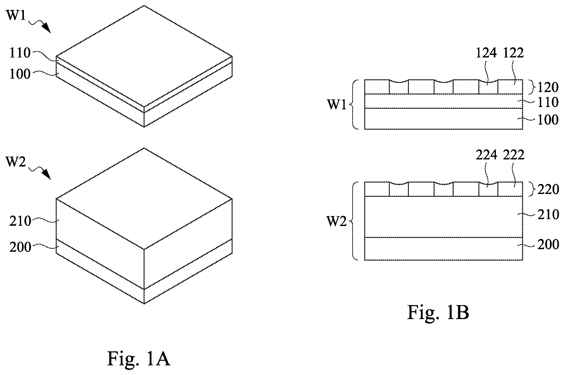
The following disclosure provides many different embodiments, or examples, for implementing different features of the provided subject matter. Specific examples of components and arrangements are described below to simplify the present disclosure. These are, of course, merely examples and are not intended to be limiting. For example, the formation of a first feature over or on a second feature in the description that follows may include embodiments in which the first and second features are formed in direct contact, and may also include embodiments in which additional features may be formed between the first and second features, such that the first and second features may not be in direct contact. In addition, the present disclosure may repeat reference numerals and/or letters in the various examples. This repetition is for the purpose of simplicity and clarity and does not in itself dictate a relationship between the various embodiments and/or configurations discussed. Further, spatially relative terms, such as “beneath,” “below,” “lower,” “above,” “upper” and the like, may be used herein for ease of description to describe one element or feature's relationship to another element(s) or feature(s) as illustrated in the figures. The spatially relative terms are intended to encompass different orientations of the device in use or operation in addition to the orientation depicted in the figures. The apparatus may be otherwise oriented (rotated 90 degrees or at other orientations) and the spatially relative descriptors used herein may likewise be interpreted accordingly. A to 6 B are schematic views of a wafer bonding method at different stages in accordance with some embodiments of the present disclosure, in which B, 2 B, 3 B, 4 B, 5 B, and 6 B are cross-sectional view of A, 2 A, 3 A, 4 A, 5 A, and 6 A , respectively. Moreover, some elements (e.g., bonding layers 120 and 220 ) of B, 2 B, 3 B, 4 B, 5 B, and 6 B are not illustrated in A, 2 A, 3 A, 4 A, 5 A, and 6 A for brevity. Referring to A and 1 B , shown there are a wafer W 1 and a wafer W 2 . In some embodiments, the wafers W 1 and W 2 can be manufactured through several semiconductor processes. The semiconductor processes may include deposition, patterning, etching, or other suitable processes, so as to form functional circuits over the wafers W 1 and W 2 . The wafers W 1 and W 2 include substrates 100 and 200 , respectively. In some embodiments, the substrates 100 and 200 can be semiconductor substrates. The semiconductor substrate may be bulk silicon substrate or silicon-on-insulator (SOI) substrate. In accordance with alternative embodiments of the present disclosure, other semiconductor materials that include group III, group IV, and/or group V elements may also be used, which may include silicon germanium, silicon carbon, and/or III-V compound semiconductor materials. Semiconductor device 110 is over the substrate 100 of the wafer W 1 , and semiconductor device 210 is over the substrate 200 of the wafer W 2 . In some embodiments, the semiconductor devices 110 and 210 may include electrical components, such as transistors, diodes, resistors, capacitors, etc. In some embodiments, the semiconductor device 110 may include memory array, which may include NAND type non-volatile memory. In some embodiments, the memory array of the NAND type non-volatile memory may include three-dimensional (3D) arrangement configuration. In other embodiments, the memory array may also include NOR type or AND type memory array. On the other hand, the semiconductor device 210 may include complementary metal-oxide-semiconductor (CMOS) devices. Referring to B , the wafers W 1 and W 2 further includes bonding layers 120 and 220 , respectively, in which the bonding layer 120 of the wafer W 1 will be bonded to the bonding layer 220 of the wafer W 2 in the following discussed bonding process. In some embodiments, the bonding layer 120 includes a dielectric layer 122 and a plurality of conductive pads 124 in the dielectric layer 122 . Similarly, the bonding layer 220 includes a dielectric layer 222 and a plurality of conductive pads 224 in the dielectric layer 222 . In some embodiments, the bonding layer 120 may also be referred to as interconnect layer, in which the bonding layer 120 is a topmost layer of the wafer W 1 , and the conductive pads 124 of the bonding layer 120 are electrically connected to the electrical components within the semiconductor device 110 . Similarly, the bonding layer 220 may also be referred to as interconnect layer, in which the bonding layer 220 is a topmost layer of the wafer W 2 , and the conductive pads 224 of the bonding layer 220 are electrically connected to the electrical components within the semiconductor device 210 . During the following discussed bonding process, the conductive pads 124 of the bonding layer 120 are bonded to the conductive pads 224 of the bonding layer 220 , to further electrically connect the semiconductor device 110 of the wafer W 1 and the semiconductor device 210 of the wafer W 2 with each other. In some embodiments, the materials of the dielectric layers 122 and 222 may include silicon oxide, silicon nitride, silicon oxy-nitride, tetraethoxysilane (TEOS), phosphosilicate glass (PSG), borophosphosilicate glass (BPSG), low-k dielectric material and/or other suitable dielectric materials. In some embodiments, the conductive pads 124 and 224 may include metal materials, such as copper (Cu). In other embodiments, the conductive pads 124 and 224 may also include aluminum (Al), tungsten (W), or other suitable metal materials. A to 4 B will discuss a bonding process between the wafers W 1 and W 2 . The bonding process discussed in A to 4 B can be referred to as hybrid bonding or metal-to-metal bonding. In some embodiments where the conductive pads 124 and 224 are made of Cu, the bonding process may also be referred to as Cu-to-Cu bonding. In some embodiments, prior to the bonding process discussed in A to 4 B , cleaning process and plasma treatment may be performed to the wafers W 1 and W 2 , in which the cleaning process is used to remove the native oxides over the conductive pads 124 and 224 , and the plasma treatment is used to activate the conductive pads 124 and 224 . Referring to A and 2 B , one of the wafers W 1 and W 2 is flipped over. For example, in the embodiments of A and 2 B , the wafer W 2 is flipped over by 180 degrees, such that the bonding layer 220 of the wafer W 2 faces the bonding layer 120 of the wafer W 1 . In greater detail, the conductive pads 224 of the bonding layer 220 of the wafer W 2 are aligned with the conductive pads 124 of the bonding layer 120 of the wafer W 1 . In some embodiments, the wafers W 1 and W 2 may be bonded together using a bonder. For example, the bonder may include a first wafer supporter and a second wafer supporter, which are configured to support the wafers W 1 and W 2 , respectively. Then, alignment marks on the wafers W 1 and W 2 are measured to record the positions of the wafers W 1 and W 2 . Afterwards, based on the recorded positions of the wafers W 1 and W 2 , the wafer W 1 is aligned with the wafer W 2 . Referring to A and 3 B , the wafers W 1 and W 2 are bonded, such that the bonding layer 120 of the wafer W 1 is in contact with the bonding layer 220 of the wafer W 2 . The above mentioned bonder may be used to press the wafers W 1 and W 2 against each other. In greater detail, the conductive pads 124 of the bonding layer 120 of the wafer W 1 are in contact with the corresponding conductive pads 224 of the bonding layer 220 of the wafer W 2 , respectively. In some embodiments, the bonding step of A and 3 B can be referred to as temporary bonding. This is because at this step, the wafer W 2 is lightly pressed against the wafer W 1 , such that the wafer W 1 is in contact with the wafer W 2 . That is, during the temporary bonding, there is no strong bonding force between the wafers W 1 and W 2 . As a result, a de-bonding process can be performed to separate the wafers W 1 and W 2 , and would not destroy the bonding layers 120 and 220 . In some embodiments, the bonding step of A and 3 B is performed under room temperature (such as about 25° C. to about 27° C.). Referring to A and 4 B , a first process P 1 is performed. In some embodiments, the first process P 1 is an annealing process. In the embodiments where the first process P 1 is an annealing process, the annealing process causes inter-diffusion between the metal material of the conductive pads 124 and the metal material of the corresponding conductive pads 224 , such that the conductive pads 124 and the corresponding conductive pads 224 are tightly bonded with each other. In some embodiments, the temperature of the annealing process is greater than the temperature of the temporary bonding as discussed in A and 3 B . Referring to A and 5 B , a second process P 2 is performed to the substrate 200 of the wafer W 2 . In some embodiments, the second process P 2 is a grinding process, so as to reduce the thickness of the substrate 200 . Referring to A and 6 B , conductive features 230 are formed in the substrate 200 of the wafer W 2 . The conductive features 230 may penetrate through the substrate 200 and are electrically connected with the semiconductor device 210 of the wafer W 2 . In some embodiments, the conductive features 230 may be formed by patterning the substrate 200 to form openings in the substrate 200 , filling conductive materials in the openings, and then performing a polishing process until the substrate 200 is exposed. In some embodiments, the conductive features 230 may include metal materials, such as copper (Cu). In other embodiments, the conductive features 230 may also include aluminum (Al), tungsten (W), or other suitable metal materials. In some embodiments, the conductive features 230 may also be referred to as through silicon vias (TSVs). A and 7 B are schematic views of wafer bonding in accordance with some embodiments of the present disclosure. It is noted that some elements of A and 7 B are the same as those discussed in A to 6 B , such elements are labeled the same, and relevant details will not be repeated for brevity. A and 7 B are schematic views of bonding between the wafers W 1 and W 2 . In greater detail, conductive pads 124 A, 124 B, and 124 C are disposed in the dielectric layer 122 of the wafer W 1 . Moreover, the wafer W 1 also includes a dielectric layer 132 and conductive vias 134 A, 134 B, and 134 C in the dielectric layer 132 , in which the conductive vias 134 A, 134 B, and 134 C are in contact with the conductive pads 124 A, 124 B, and 124 C, respectively. Similarly, conductive pads 224 A, 224 B, and 224 C are disposed in the dielectric layer 222 of the wafer W 2 . Moreover, the wafer W 2 also includes a dielectric layer 232 and conductive vias 234 A, 234 B, and 234 C in the dielectric layer 232 , in which the conductive vias 234 A, 234 B, and 234 C are in contact with the conductive pads 224 A, 224 B, and 224 C, respectively. In some embodiments, the dielectric layer 132 and the conductive vias 134 A, 134 B, and 134 C may be referred to as an interconnect layer. Moreover, the dielectric layer 232 and the conductive vias 234 A, 234 B, and 234 C may be referred to as an interconnect layer. A shows an ideal condition, in which the ideal condition is resulted from that the wafers W 1 and W 2 are not distorted during the manufacturing processes. Thus, elements of the wafers W 1 and W 2 are substantially at ideal positions, such that the wafers W 1 and W 2 may be bonded with each other as predicted. For example, the conductive pad 124 A (and conductive via 134 A) of the wafer W 1 and the conductive pad 224 A (and conductive via 234 A) of the wafer W 2 are both at an ideal position I 1 , such that conductive pad 124 A of the wafer W 1 would be in contact with the conductive pad 224 A of the wafer W 2 after bonding. The conductive pad 124 B (and conductive via 134 B) of the wafer W 1 and the conductive pad 224 B (and conductive via 234 B) of the wafer W 2 are both at an ideal position I 2 , such that conductive pad 124 B of the wafer W 1 would be in contact with the conductive pad 224 B of the wafer W 2 after bonding. The conductive pad 124 C (and conductive via 134 C) of the wafer W 1 and the conductive pad 224 C (and conductive via 234 C) of the wafer W 2 are both at an ideal position I 3 , such that conductive pad 124 C of the wafer W 1 would be in contact with the conductive pad 224 C of the wafer W 2 after bonding. B shows a real condition in accordance with some embodiments of the present disclosure. Different from A , during the manufacturing processes, the wafers W 1 and W 2 may be distorted, such as warpage. As an example of B , the wafers W 1 and W 2 may be bended during the manufacturing processes. As a result, during the bonding process, although the force applied to the wafers W 1 and W 2 may flatten the wafers W 1 and W 2 , it may also cause displacement to the patterns of the wafers W 1 and W 2 . For example, in B , the conductive pad 124 A (and the conductive via 134 A) is shifted toward the −X direction by S 1 _A with respect to the ideal position I 1 , and the conductive pad 124 C (and the conductive via 134 C) is shifted toward the +X direction by S 1 _C with respect to the ideal position I 3 . On the other hand, the conductive pad 224 A (and the conductive via 234 A) is shifted toward the +X direction by S 2 _A with respect to the ideal position I 1 , and the conductive pad 224 C (and the conductive via 234 C) is shifted toward the −X direction by S 2 _C with respect to the ideal position I 3 . The above condition may result in that the conductive pad 124 A of the wafer W 1 and the conductive pad 224 A of the wafer W 2 may not be in contact with each other (or the contact area is less than a predetermined value) after bonding. Similarly, the conductive pad 124 C of the wafer W 1 and the conductive pad 224 C of the wafer W 2 may not be in contact with each other (or the contact area is less than a predetermined value) after bonding. Such condition may be referred to as overlay error, which will result in an unsatisfied electrical connection. In some embodiments, the predetermined value of the contact area may be 50% of the junction area of one of the conductive pad 124 A and the conductive pad 224 A. In some embodiments, the predetermined value of the contact area may be 30% of the junction area of one of the conductive pad 124 A and the conductive pad 224 A. Here, the “junction area” may be referred to as the total area of the conductive pad 124 A (or the conductive pad 224 A) that is used to bonded with the conductive pad 224 A (or the conductive pad 124 A). The predetermined value of the contact area between the conductive pad 124 C and the conductive pad 224 C may include similar relationship, and will not be repeated for brevity. In some embodiments, the conductive pad 124 B of the wafer W 1 and the conductive pad 224 B of the wafer W 2 are substantially aligned with an ideal position I 2 . Thus, the conductive pad 124 B of the wafer W 1 may be in contact with the conductive pad 224 B of the wafer W 2 to create a satisfied electrical connection. A to 8 D are schematic views of overlay error in accordance with some embodiments of the present disclosure. A, 8 B, 8 C, and 8 D show overlay error conditions of translation, rotation, scaling, and random, respectively. In some embodiments, the overlay error conditions of translation, rotation, and scaling of A, 8 B, and 8 C can be fixed by a compensation method to improve the bonding between the wafers W 1 and W 2 . For example, the compensation method may include adjusting the relative positions of wafers W 1 and W 2 to improve the bonding between the wafers W 1 and W 2 . In the condition of A , the relative positions of wafers W 1 and W 2 can be adjusted by linearly moving the wafer W 1 (or wafer W 2 ). In the condition of B , the relative positions of wafers W 1 and W 2 can be adjusted by rotating the wafer W 1 (or wafer W 2 ). In the condition of C , the relative positions of wafers W 1 and W 2 can be adjusted by scaling up (or scaling down) the wafer W 1 (or wafer W 2 ). For example, the center of the wafer W 1 (or the wafer W 2 ) may be applied with a force, such that the wafer W 1 may be radially enlarged (or shrunk) from the center to the edge. The above compensation method can be conducted by adjusting the bonding process to improve the bonding between the wafers W 1 and W 2 . For example, referring to B , by performing the above compensation method, the conductive pads 124 A and 124 C of the wafer W 1 can be in contact with the conductive pads 224 A and 224 C of the wafer W 2 . In some conditions, such as the deformation of the wafer is too severe due to the manufacturing process, the bonder may not be able to fully compensate the error of wafer scaling up (or scaling down) by applying a center force, and this may result in that the overlay of the wafers W 1 and W 2 is less than a predetermined level. Moreover, referring to D , in some embodiments, the random error may not be fixed by using the above compensation method to improve the bonding between the wafers W 1 and W 2 as well. As a result, another compensation method is needed to improve the bonding between the wafers W 1 and W 2 . is a schematic view of a lithography process in accordance with some embodiments of the present disclosure. A is a schematic view of bonding result in accordance with some embodiments of the present disclosure. B to 10 E are schematic views of compensation methods in accordance with some embodiments of the present disclosure. In greater detail, B to 10 E provide different compensation methods, in which the compensation methods are conducted, based on the bonding result of A , by individually adjusting the exposure shift on different fields of the wafer, so as to obtain a better bonding quality. Referring to , shown there is the wafer W 1 (or wafer W 2 ), in which wafer W 1 includes several exposure fields A. During the lithography process, lithography tool 500 (or scanner) may include a light source, the lithography tool 500 may pass the light generated from the light source to an exposure field A of the wafer W 1 through a photomask, so as to transfer the pattern of the photomask to a material layer (such as photoresist) within the exposure field A of the wafer W 1 . The pattern may define the positions of elements on the wafer W 1 , such as the positions of the conductive pads 124 A, 124 B, and 124 C. For example, by forming a photoresist layer over the dielectric layer 122 of the wafer W 1 , performing an exposure process to the photoresist layer to transfer the pattern of the photomask onto the photoresist layer, etching the dielectric layer 122 through the pattern of the photoresist layer to form openings, in which the shapes and the positions of the openings correspond to the pattern of the photoresist layer. Finally, the conductive pads 124 A, 124 B, and 124 C are formed in the openings. In other words, the positions of the conductive pads 124 A, 124 B, and 124 C are defined by the exposure process of the lithography process. Accordingly, by adjusting the exposure position, the positions of the conductive pads 124 A, 124 B, and 124 C on the wafer W 1 can be changed. Similarly, by adjusting the exposure position, the positions of the conductive pads 224 A, 224 B, and 224 C on the wafer W 2 can be changed. Referring to A , in which A is the same as B . In some embodiments, the conductive pads 124 A, 124 B, and 124 C of the wafer W 1 may correspond to different exposure fields of the wafer W 1 . For example, the conductive pad 124 A may correspond to the exposure field A 1 of the wafer W 1 , the conductive pad 124 B may correspond to the exposure field A 2 of the wafer W 1 , and conductive pad 124 C may correspond to the exposure field A 3 of the wafer W 1 . That is, during the exposure process of the lithography process, the position of the conductive pad 124 A is defined by performing a first exposure step to the exposure field A 1 of the wafer W 1 , the position of the conductive pad 124 B is defined by performing a second exposure step to the exposure field A 2 of the wafer W 1 , and the position of the conductive pad 124 C is defined by performing a third exposure step to the exposure field A 3 of the wafer W 1 . The first, second, and third exposure steps are performed at different time points, and thus the positions of the conductive pads 124 A, 124 B, and 124 C can be adjusted individually. In some embodiments, the exposure field A 2 is at the center region of the wafer W 1 , and the exposure fields A 1 and A 3 are at the edge regions of the wafer W 1 , while the present disclosure is not limited thereto. Similarly, the positions of the conductive pads 224 A, 224 B, and 224 C of the wafer W 2 may also be defined by different exposure steps of the lithography process, and thus relevant details will not be repeated. Referring to B , a compensation method is performed based on the bonding result of the wafers W 1 and W 2 of A , so as to produce a new wafer W 1 ′ and a new wafer W 2 ′. Referring to the wafer W 1 ′, the conductive pad 124 A′ of the wafer W 1 ′ is shifted with respect to the conductive pad 124 A of the wafer W 1 by S 1 _A, and the conductive pad 124 C′ of the wafer W 1 ′ is shifted with respect to the conductive pad 124 C of the wafer W 1 by S 1 _C. That is, during the first exposure step for forming the conductive pad 124 A′, the exposure of the exposure field A 1 can be shifted by S 1 _A. During the third exposure step for forming the conductive pad 124 C′, the exposure of the exposure field A 3 can be shifted by S 1 _C. In some embodiments, because the shifts S 1 _A and S 1 _C are defined by different exposure steps, the shifts S 1 _A and S 1 _C may include different directions and different magnitudes, which is beneficial to improve the flexibility of adjusting the positions of the conductive pads. Similarly, the conductive pad 224 A′ of the wafer W 2 ′ is shifted with respect to the conductive pad 224 A of the wafer W 2 by S 2 _A, and the conductive pad 224 C′ of the wafer W 2 ′ is shifted with respect to the conductive pad 224 C of the wafer W 2 by S 2 _C. That is, during the first exposure step for forming the conductive pad 224 A′, the exposure of the exposure field A 1 can be shifted by S 2 _A. During the third exposure step for forming the conductive pad 224 C′, the exposure of the exposure field A 3 can be shifted by S 2 _C. In some embodiments, because the shifts S 2 _A and S 2 _C are defined by different exposure steps, the shifts S 2 _A and S 2 _C may include different directions and different magnitudes, which is beneficial to improve the flexibility of adjusting the positions of the conductive pads. In some embodiments, the position of the conductive pad 124 B′ of the wafer W 1 ′ is substantially the same as the position of the conductive pad 124 B of the wafer W 1 . Similarly, the position of the conductive pad 224 B′ of the wafer W 2 ′ is substantially the same as the position of the conductive pad 224 B of the wafer W 2 . That is, during the second exposure for forming the conductive pad 124 B′ (or conductive pad 224 B′), there is no shift to the exposure field A 2 . After the compensation method of B is completed, the conductive pads 124 A′, 124 B′, and 124 C′ of the wafer W 1 ′ would be in contact with the conductive pads 224 A′, 224 B′, and 224 C′ of the wafer W 2 ′ after the bonding process. Accordingly, the compensated wafers W 1 ′ and W 2 ′ improve the overlay error of the wafers W 1 and W 2 as discussed in A . Referring to C , a compensation method is performed based on the bonding result of the wafers W 1 and W 2 of A , so as to produce a new wafer W 1 ′ and a new wafer W 2 ′. Different from B , the compensation method of C is performed only to the wafer W 2 ′, and is not performed to the wafer W 1 ′. That is, the processing condition of the wafer W 1 ′ is substantially the same as the processing condition of the wafer W 1 . In greater detail, the positions of the conductive pads 124 A′, 124 B′, and 124 C′ of the wafer W 1 ′ are the same as the positions of the conductive pads 124 A, 124 B, and 124 C of the wafer W 1 . The compensation method performed to the wafer W 2 ′ is similar to those described in B , and thus relevant details will not be repeated. After the compensation method of C is completed, the conductive pads 124 A′, 124 B′, and 124 C′ of the wafer W 1 ′ would be in contact with the conductive pads 224 A′, 224 B′, and 224 C′ of the wafer W 2 ′ after the bonding process. Accordingly, the compensated wafers W 1 ′ and W 2 ′ improve the overlay error of the wafers W 1 and W 2 as discussed in A . In some embodiments, because the compensation method is performed only to the wafer W 2 ′, and thus the wafer W 1 ′ may not be a new wafer. As mentioned above, during the temporary bonding discussed in A , the wafers W 1 and W 2 are not tightly bonded, a de-bonding process may be performed to separate the wafers W 1 and W 2 , and would not destroy the wafers W 1 and W 2 . Accordingly, the compensated wafer W 2 ′ may be bonded to the original wafer W 1 , so as to prevent discarding the original wafer W 1 . Referring to D , a compensation method is performed based on the bonding result of the wafers W 1 and W 2 of A , so as to produce a new wafer W 1 ′ and a new wafer W 2 ′. Different from B , the compensation method of D is performed only to the wafer W 1 ′, and is not performed to the wafer W 2 ′. That is, the processing condition of the wafer W 2 ′ is substantially the same as the processing condition of the wafer W 2 . In greater detail, the positions of the conductive pads 224 A′, 224 B′, and 224 C′ of the wafer W 2 ′ are the same as the positions of the conductive pads 224 A, 224 B, and 224 C of the wafer W 2 . The compensation method performed to the wafer W 1 ′ is similar to those described in B , and thus relevant details will not be repeated. After the compensation method of D is completed, the conductive pads 124 A′, 124 B′, and 124 C′ of the wafer W 1 ′ would be in contact with the conductive pads 224 A′, 224 B′, and 224 C′ of the wafer W 2 ′ after the bonding process. Accordingly, the compensated wafers W 1 ′ and W 2 ′ improve the overlay error of the wafers W 1 and W 2 as discussed in A . In some embodiments, because the compensation method is performed only to the wafer W 1 ′, and thus the wafer W 2 ′ may not be a new wafer. As mentioned above, during the temporary bonding discussed in A , the wafers W 1 and W 2 are not tightly bonded, a de-bonding process may be performed to separate the wafers W 1 and W 2 , and would not destroy the wafers W 1 and W 2 . Accordingly, the compensated wafer W 1 ′ may be bonded to the original wafer W 2 , so as to prevent discarding the original wafer W 2 . Referring to E , a compensation method is performed based on the bonding result of the wafers W 1 and W 2 of A , so as to produce a new wafer W 1 ′ and a new wafer W 2 ′. The compensation method of E is similar to the compensation method of B , in which both the wafers W 1 ′ and W 2 ′ are compensated. However, in the embodiments of B , the shift S 1 _A, the shift S 1 _C, the shift S 2 _A, and the shift S 2 _C are determined by the ideal positions of the conductive pads 124 A, 124 C, 224 A, and 224 C (as discussed in B ), respectively. The conductive pads 124 A′, 124 C′, 224 A′, and 224 C′ of the wafers W 1 ′ and W 2 ′ are moved toward the ideal positions, such that the conductive pad 124 A′ can be completely aligned with the conductive pad 224 A′, and the conductive pad 124 C′ can be completely aligned with the conductive pad 224 C′. However, this may result in that the conductive pads 124 A′, 124 C′, 224 A′, and 224 C′ are shifted from the corresponding conductive vias 134 A, 134 C, 234 A, and 234 C, respectively. If the shifts are too large, additional electrical connection issues may occur. Accordingly, in the compensation method of E , the conductive pad 124 A′ of the wafer W 1 ′ is shifted with respect to the conductive pad 124 A of the wafer W 1 by S 1 _A′, in which the shift S 1 _A′ is less than the shift S 1 _A discussed in B . The conductive pad 124 C′ of the wafer W 1 ′ is shifted with respect to the conductive pad 124 C of the wafer W 1 by S 1 _C′, in which the shift S 1 _C′ is less than the shift S 1 _C discussed in B . Similarly, the conductive pad 224 A′ of the wafer W 2 ′ is shifted with respect to the conductive pad 224 A of the wafer W 2 by S 2 _A′, in which the shift S 2 _A′ is less than the shift S 2 _A discussed in B . The conductive pad 224 C′ of the wafer W 2 ′ is shifted with respect to the conductive pad 224 C of the wafer W 2 by S 2 _C′, in which the shift S 2 _C′ is less than the shift S 2 _C discussed in B . The above method may ensure that the conductive pads 124 A′ and 224 A′ are in partial contact, and the conductive pads 124 C′ and 224 C′ are in partial contact. On the other hand, the method also ensures that the conductive pads 124 A′, 124 C′, 224 A′, and 224 C′ and the corresponding conductive vias 134 A′, 134 C′, 234 A′, and 234 C′ maintain reliable electrical connections. Referring to B and 10 E , in some embodiments, after using the compensation method of B to produce the compensated wafers W 1 ′ and W 2 ′, and overlay check may be performed to the compensated wafers W 1 ′ and W 2 ′, so as to determine whether elements of the wafers W 1 ′ and W 2 ′ include reliable electrical connections. For example, it is determined that whether the conductive pads 124 A′, 124 C′, 224 A′, and 224 C′ are in contact with the corresponding conductive vias 134 A′, 134 C′, 234 A′, and 234 C′. If the conductive pads 124 A′, 124 C′, 224 A′, and 224 C′ are not in contact with the corresponding conductive vias 134 A′, 134 C′, 234 A′, and 234 C′ (or the contact area is less than a predetermined value), the method discussed in B should be modified. In some embodiments, the method discussed in E can be used to replace the method discussed in B . In some embodiments, the predetermined value of the contact area may be 50% of the junction area of one of the conductive pad 124 A′ and the conductive via 134 A. In some embodiments, the predetermined value of the contact area may be 30% of the junction area of one of the conductive pad 124 A′ and the conductive via 134 A. Here, the “junction area” may be referred to as the total area of the conductive pad 124 A (or the conductive via 134 A) that is used to bonded with the conductive via 134 A (or the conductive pad 124 A). The predetermined value of the contact area between the conductive pad 124 C′ and the conductive via 134 C, the predetermined value of the contact area between the conductive pad 224 A′ and the conductive via 234 A, and the predetermined value of the contact area between the conductive pad 224 C′ and the conductive via 234 C may include similar relationship, and will not be repeated for brevity. is a flow chart of a compensation method in accordance with some embodiments of the present disclosure. is a block diagram of a compensation method in accordance with some embodiments of the present disclosure. Although is described as a series of acts, it will be appreciated that these acts are not limiting in that the order of the acts can be altered in other embodiments, and the methods disclosed are also applicable to other structures. In other embodiments, some acts that are illustrated and/or described may be omitted in whole or in part. It is noted that, the first compensation method and the second compensation method of merely indicate that they are compensation methods at different stages, and would not limit the order thereof. Similarly, the first overlay check, the second overlay check, and the third overlay check of merely indicate that they are overlay checks at different stages, and would not limit the order thereof. The method M 1 of starts from step S 101 by forming semiconductor devices over wafers. For example, referring to A and 1 B , semiconductor device 110 can be formed over the substrate 100 of the wafer W 1 , and semiconductor device 210 can be formed over the substrate 200 of the wafer W 2 . In other embodiments, the step S 101 may also include forming interconnect structures over the wafers, such as the dielectric layers 132 and 232 , and the conductive vias 134 A to 134 C and 234 A to 234 C of A . The method proceeds to step S 102 by forming bonding layers over the wafers. For example, referring to A and 1 B , bonding layers 120 and 220 are formed over the wafers W 1 and W 2 , respectively. In some embodiments, the bonding layers 120 and 220 may be formed using the lithography tool 310 (or scanner) of . For example, the positions of the conductive pads 124 and 224 of the bonding layers 120 and 220 are defined by the lithography tool 310 . The method proceeds to step S 103 by performing a temporary bonding. For example, referring to A to 3 B , a temporary bonding may be performed to the wafers W 1 and W 2 . In some embodiments, the temporary bonding can be performed using the bonder 320 of . For example, the bonder 320 may include a first wafer supporter and a second wafer supporter, which are configured to support the wafers W 1 and W 2 , respectively. Then, by measuring the alignment marks on the wafers W 1 and W 2 to record the positions of the wafers W 1 and W 2 . Afterwards, based on the recorded positions of the wafers W 1 and W 2 , the wafer W 1 is aligned with the wafer W 2 . Finally, the wafers W 1 and W 2 are pressed against each other, such that the wafers W 1 and W 2 are in contact with each other. During the temporary bonding, the wafers W 1 and W 2 are not tightly bonded, and thus the wafers W 1 and W 2 can still be de-bonded from each other. The method proceeds to step S 104 by performing a first overlay check, and determining whether a result of the first overlay check is within a predetermined specification. In some embodiments, the first overlay check includes determining the bonding layers 120 and 220 of the wafers W 1 and W 2 form an electrical connection as predicted. For example, as shown in A and 7 B, the first overlay check includes determining whether the conductive pads 124 A, 124 B, and 124 C of wafer W 1 are in contact with the respective conductive pads 224 A, 224 B, and 224 C of wafer W 2 , respectively. If the conductive pads 124 A, 124 B, and 124 C of wafer W 1 are all in contact with (or the contact area is greater than a predetermined value) the respective conductive pads 224 A, 224 B, and 224 C of wafer W 2 , the result of the first overlay check is determined as within the predetermined specification (IN SPEC). However, if one of the conductive pads 124 A, 124 B, and 124 C of wafer W 1 is not in contact with (or the contact area is less than a predetermined value) the respective one of the conductive pads 224 A, 224 B, and 224 C of wafer W 2 , the result of the first overlay check is determined as beyond the predetermined specification (OUT SPEC). If the result of the first overlay check of step S 104 is determined as within the predetermined specification, the method proceeds to step S 105 by performing a first process. In some embodiments, the first process may be the first process P 1 as discussed in A and 4 B , such as an annealing process. Then, after the step S 105 , the method proceeds to step S 106 by performing a second process. In some embodiments, the second process may be the second process P 2 as discussed in A and 5 B , such as a grinding process, or the process as discussed in A and 6 B , and thus relevant details will not be repeated. In , the wafers W 1 and W 2 , which are determined as within the predetermined specification, can be transferred to other processing device 340 for the second process. Referring back to step S 104 , if the result of the first overlay check of step S 104 is determined as beyond the predetermined specification, the method proceeds to step S 107 by performing a first compensation method. If the result of the first overlay check is determined as beyond the predetermined specification, this may indicate that overlay error occurs. For example, one of the conductive pads 124 A, 124 B, and 124 C of wafer W 1 is not in contact with (or the contact area is less than a predetermined value) the respective one of the conductive pads 224 A, 224 B, and 224 C of wafer W 2 . Because the wafers W 1 and W 2 are under temporary bonding, the first compensation method includes separating the wafers W 1 and W 2 using the bonder 320 of . Then, the first compensation method may include the compensation methods as discussed in A to 8 C , and thus relevant details will not be repeated. In some embodiments, the first compensation method may be performed using the bonder 320 , which includes separating the wafers W 1 and W 2 , adjusting relative positions of the wafers W 1 and W 2 , and then re-bonding the wafers W 1 and W 2 . The method proceeds to step S 108 by performing a second overlay check, and determining whether a result of the second overlay check is within a predetermined specification. In greater detail, the second overlay check is performed after the first compensation method. In some embodiments, the second overlay check includes determining whether the bonding layers 120 and 220 of the compensated wafers W 1 and W 2 form an electrical connection as predicted. Details of the second overlay check may be similar to those described with respect to the first overlay check, and thus relevant details will not be repeated. In some embodiments, the second overlay check may be performed by the overlay check stage 330 of . If the result of the second overlay check of step S 108 is determined as within the predetermined specification, the method proceeds to step S 105 by performing a first process. Then, after step 105 , the method proceeds to step S 106 by performing a second process. If the result of the second overlay check of step S 108 is determined as beyond the predetermined specification, the method proceeds to step S 109 by performing a second compensation method. In some embodiments, the second compensation method may include the compensation methods as discussed in B to 10 E , and thus relevant details will not be repeated. In some embodiments, the second compensation method includes designing compensated wafers W 1 ′ and W 2 ′, such that the compensated wafers W 1 ′ and W 2 ′ include better bonding result. For example, the second compensation method may include modifying the positions of the conductive pads 124 A to 124 C and the positions of the conductive pads 224 A to 224 C of A to the positions of the conductive pads 124 A′ to 124 C′ and the positions of the conductive pads 224 A′ to 224 C′ of B to 10 E , respectively. The method proceeds to step S 110 by manufacturing wafers based on the second compensation method. In some embodiments, compensated wafers W 1 ′ and/or W 2 ′ can be re-produced based on the compensation methods as discussed in B to 10 E . In some embodiments, the lithography tool 310 of may be used to define the positions of the conductive pads 124 A′ to 124 C′ and the positions of the conductive pads 224 A′ to 224 C′ of B to 10 E on the compensated wafers W 1 ′ and W 2 ′, respectively. The method proceeds to step S 111 by performing a third overlay check, and determining whether a result of the third overlay check is within a predetermined specification. In some embodiments, the third overlay check is different from the first overlay check and the second overlay check discussed above. For example, the first overlay check and the second overlay check may include using suitable method to detect the bonding condition between wafers W 1 and W 2 (or wafers W 1 ′ and W 2 ′). The third overlay check includes determining whether the conductive pads 124 A′ to 124 C′ of the wafer W 1 ′ are in contact with the respective conductive vias 134 A to 134 C, and determining whether the conductive pads 224 A′ to 224 C′ of the wafer W 2 ′ are in contact with the respective conductive vias 234 A to 234 C. If the conductive pads 124 A′, 124 B′, and 124 C′ of the wafer W 1 ′ are all in contact with (or the contact area is greater than a predetermined value) the respective conductive vias 134 A to 134 C, the result of the third overlay check is determined as within the predetermined specification (IN SPEC). However, if one of the conductive pads 124 A′, 124 B′, and 124 C′ of the wafer W 1 ′ is not in contact with (or the contact area is less than a predetermined value) the respective one of the conductive vias 134 A to 134 C, the result of the third overlay check is determined as beyond the predetermined specification (OUT SPEC). Performing the third overlay check to the wafer W 2 ′ is similar to those described with respect to the wafer W 1 ′, and thus relevant details will not be repeated. In some embodiments, the third overlay check can be performed using the overlay check stage 330 of . If the result of the third overlay check is determined as within the predetermined specification, the method proceeds to step S 103 . Here, a temporary bonding can be performed to the compensated wafers W 1 ′ and W 2 ′. Then, the method can proceed to step S 104 (and the following steps) to complete the bonding between the wafers W 1 ′ and W 2 ′. If the result of the third overlay check is determined as beyond the predetermined specification, the method proceeds to step S 108 . In some embodiments, if the result of the third overlay check is determined as beyond the predetermined specification, the second compensation method is redone, and the result of the redone second compensation method is different from the result of the previous second compensation method. For example, the wafers W 1 ′ and W 2 ′ may be manufactured using the compensation method as discussed in B . If the result overlay check for the structure of B is beyond the predetermined specification, the compensation method of B can be modified with the compensation method of E , so as to produce other wafers W 1 ′ and W 2 ′. Referring to , the result generated from the overlay check stage 330 can be sent to an advanced process control (APC) system 350 . Moreover, also includes patterned wafer geometry (PWG) stage 360 and PWG stage 370 . In some embodiments, the PWG stages 360 and 370 may include wafer shape monitor for measuring the wafer shape, such as wafer warpage. In some embodiments, the PWG stage 360 may be used to measure the wafer shapes of the wafers W 1 and W 2 (or the wafers W 1 ′ and W 2 ′) prior to performing the step S 102 . In greater detail, prior to forming the bonding layers 120 and 220 , the shapes of the wafers W 1 and W 2 (or the wafers W 1 ′ and W 2 ′) are measured. On the other hand, the PWG stage 370 may be used to measure the wafer shapes of the wafers W 1 and W 2 (or the wafers W 1 ′ and W 2 ′) after performing the step S 102 . In greater detail, after forming the bonding layers 120 and 220 , the wafer shapes of the wafers W 1 and W 2 (or the wafers W 1 ′ and W 2 ′) are measured. For example, each time when performing the method M 1 , several wafer shape data of the wafers W 1 and W 2 (or the wafers W 1 ′ and W 2 ′) can be recorded using the PWG stage 360 , and several wafer shape data of the wafers W 1 and W 2 (or the wafers W 1 ′ and W 2 ′) can be recorded using the PWG stage 370 . Then, the APC system 350 may collect the data from the PWG stages 360 and 370 and the overlay check stage 330 . The lithography tool 310 and the bonder 320 can adjusting the first compensation method and the second compensation method based on the collected data, so as to obtain a better bonding quality. is a flow chart of a compensation method in accordance with some embodiments of the present disclosure. is a schematic view of a compensation method in accordance with some embodiments of the present disclosure. is a block diagram of a compensation method in accordance with some embodiments of the present disclosure. It is noted that, the first compensation method and the second compensation method of merely indicate that they are compensation methods at different stages, and would not limit the order thereof. Similarly, the first overlay check and the second overlay check of merely indicate that they are overlay checks at different stages, and would not limit the order thereof. The method M 2 of includes step S 201 by forming semiconductor devices over wafers. The method M 2 includes step S 202 by forming bonding layers over the wafers. The method M 2 includes step S 203 by performing a temporary bonding. The method M 2 includes step S 204 by performing a performing a first overlay check performing a first overlay check, and determining whether a result of the first overlay check is within a predetermined specification. The method M 2 includes step S 205 by performing a first process. The method M 2 includes step S 206 by performing a second process. The method M 2 includes step S 207 by performing a first compensation method. The method M 2 includes step S 208 by performing a second overlay check, and determining whether a result of the second overlay check is within a predetermined specification. The steps S 201 to S 208 are similar to the steps S 101 to S 108 as discussed in , and thus relevant details will not be repeated. The method M 2 of is different from the method M 1 of , in that if the result of the first overlay check is determined as beyond the predetermined specification, the method then proceeds to step S 209 by calculating first shifts. Referring to , includes stages C 1 , C 2 , and C 3 , in which stage C 1 is a schematic view of the wafer W 1 after performing the temporary bonding (step S 203 ). In some embodiments, the first shifts are calculated when the wafer W 1 is at stage C 1 . For example, in , the position I 1 ′ of the conductive pad 124 A has a first shift SA 1 from an ideal position I 1 , and the position I 3 ′ of the conductive pad 124 C has a first shift SC 1 from an ideal position I 3 . In , the wafers W 1 and W 2 that are bonded through the bonder 320 can be transferred to the overlay check stage 330 A for conducting the first overlay check. In some embodiments, the overlay check stage 330 A may include using suitable method to detect the bonding condition between wafers W 1 and W 2 , in which the overlay check stage 330 A can be used to calculate the first shifts SA 1 and SC 1 of . Referring back to , the method then proceeds to step S 210 by performing a first process. In some embodiments, the first process may be the first process P 1 as discussed in A and 4 B , such as an annealing process. After the step S 210 , the method then proceeds to step S 211 by calculating second shifts. Referring to , the stage C 2 is a schematic view of the wafer W 1 after performing the first process (step S 210 ). In some embodiments, the second shifts are calculated when the wafer W 1 is at stage C 2 . For example, in , the position I 1 ″ of the conductive pad 124 A at stage C 2 has a second shift SA 2 from the position I 1 ′ of the conductive pad 124 A at stage C 1 , and the position I 3 ″ of the conductive pad 124 C at stage C 2 has a second shift SC 2 from the position I 3 ′ of the conductive pad 124 C at stage C 1 . In , the wafers W 1 and W 2 can be transferred to the overlay check stage 330 B for conducting an overlay check. In some embodiments, the overlay check stage 330 B may include using suitable method to detect the bonding condition between wafers W 1 and W 2 , in which the overlay check stage 330 B can be used to calculate the second shifts SA 2 and SC 2 of . After the step S 211 , the method proceeds to step S 212 by performing a second process. In some embodiments, the second process may be the second process P 2 as discussed in A and 5 B , such as a grinding process. After the step S 212 , the method then proceeds to step S 213 by calculating third shifts. Referring to , the stage C 3 is a schematic view of the wafer W 1 after performing the grinding process (step S 212 ). In some embodiments, the third shifts are calculated when the wafer W 1 is at stage C 3 . For example, in , the position I 1 ′″ of the conductive pad 124 A at stage C 3 has a third shift SA 3 from the position I 1 ″ of the conductive pad 124 A at stage C 2 , and the position I 3 ′″ of the conductive pad 124 C at stage C 3 has a third shift SC 3 from the position I 3 ″ of the conductive pad 124 C at stage C 2 . In , the wafers W 1 and W 2 can be transferred to the overlay check stage 330 C for conducting an overlay check. In some embodiments, the overlay check stage 330 C may include using suitable method to detect the bonding condition between wafers W 1 and W 2 , in which the overlay check stage 330 C can be used to calculate the second shifts SA 3 and SC 3 of . Referring back to , the method proceeds to step S 214 by performing a second compensation method. In some embodiments, the second compensation method includes designing compensated wafers W 1 ′ and W 2 ′, such that the compensated wafers W 1 ′ and W 2 ′ include better bonding result. For example, the second compensation method may include modifying the positions of the conductive pads 124 A to 124 C and the positions of the conductive pads 224 A to 224 C of A . In greater detail, referring to , the second compensation method is performed based on the first shifts of step S 209 , the second shifts of step S 211 , and the third shifts of step S 213 . For example, the position of the conductive pad 124 A′ of the compensated wafer W 1 ′ is determined by the first shift SA 1 , the second shift SA 2 , and the third shift SA 3 . In some embodiments, the conductive pad 124 A′ can be formed by shifting the conductive pad 124 A of wafer W 1 at stage C 3 , in which the shift amount may be a sum of the first shift SA 1 , the second shift SA 2 , and the third shift SA 3 (e.g., SA 1 +SA 2 +SA 3 ). In other words, the difference between the position of the conductive pad 124 A of wafer W 1 at stage C 3 and the position of the conductive pad 124 A′ of wafer W 1 ′ is substantially equal to SA 1 +SA 2 +SA 3 . Similarly, the position of the conductive pad 124 C′ of the compensated wafer W 1 ′ is determined by the first shift SC 1 , the second shift SC 2 , and the third shift SC 3 . In some embodiments, the conductive pad 124 C′ can be formed by shifting the conductive pad 124 C of wafer W 1 at stage C 3 , in which the shift amount may be a sum of the first shift SC 1 , the second shift SC 2 , and the third shift SC 3 (e.g., SC 1 +SC 2 +SC 3 ). In other words, the difference between the position of the conductive pad 124 C of wafer W 1 at stage C 3 and the position of the conductive pad 124 C′ of wafer W 1 ′ is substantially equal to SC 1 +SC 2 +SC 3 . In some embodiments of the present disclosure, because performing a first process (e.g., an annealing process) or a second process (e.g., a grinding process) may also cause warpage to the wafers W 1 and W 2 , and will further change the positions of the conductive pads. Accordingly, in the compensation method, shifts at different stages are taken into account, such that the compensated wafers have better bonding quality. It is noted that takes the wafer W 1 as an example, while in the present disclosure, the above second compensation method can also be performed to the wafer W 2 , and thus relevant details will not be repeated. In some embodiments, the steps S 212 and S 213 may be omitted. That is, the third shifts (e.g., the third shifts SA 3 and SC 3 ) are not used in the second compensation method of step S 214 . Referring back to , the method proceeds to step S 215 by manufacturing wafers based on the second compensation method. In some embodiments, the lithography tool 310 of can be used to manufacture the wafers W 1 ′ and W 2 ′. In some embodiments, the wafers W 1 ′ and W 2 ′ may be manufactured based on the above mentioned first shifts, the second shifts, and the third shifts. As discussed in , during the first exposure step for forming the conductive pad 124 A′, the exposure of the exposure field A 1 can be shifted by SA 1 +SA 2 +SA 3 to define the position of the conductive pad 124 A′. During the third exposure step for forming the conductive pad 124 C′, the exposure of the exposure field A 3 can be shifted by SC 1 +SC 2 +SC 3 to define the position of the conductive pad 124 C′. In some embodiments where the steps S 212 and S 213 are omitted, during the first exposure step for forming the conductive pad 124 A′, the exposure of the exposure field A 1 can be shifted by SA 1 +SA 2 to define the position of the conductive pad 124 A′. During the third exposure step for forming the conductive pad 124 C′, the exposure of the exposure field A 3 can be shifted by SC 1 +SC 2 to define the position of the conductive pad 124 C′. After the step S 215 , the step S 203 is performed. Here, a temporary bonding process may be performed to the compensated wafers W 1 ′ and W 2 ′. Then, the method can proceed to step S 204 (and the following steps) to complete the bonding between the wafers W 1 ′ and W 2 ′. Referring to , the results generated from the overlay check stages 330 A, 330 B, and 330 C can be transferred to the APC system 350 . Moreover, also includes PWG stages 360 and 370 . In some embodiments, the PWG stage 360 may be used to measure the shapes of the wafers W 1 and W 2 (or the wafers W 1 ′ and W 2 ′) prior to performing the step S 202 . In greater detail, prior to forming the bonding layers 120 and 220 , the shapes of the wafers W 1 and W 2 (or the wafers W 1 ′ and W 2 ′) are measured. On the other hand, the PWG stage 370 may be used to measure the shapes of the wafers W 1 and W 2 (or the wafers W 1 ′ and W 2 ′) after performing the step S 202 . In greater detail, after forming the bonding layers 120 and 220 , the shapes of the wafers W 1 and W 2 (or the wafers W 1 ′ and W 2 ′) are measured. For example, each time when performing the method M 2 , several wafer shape data of the wafers W 1 and W 2 (or the wafers W 1 ′ and W 2 ′) can be recorded using the PWG stage 360 . In some embodiments, the lithography tool 310 can initially modify the positions of the conductive pads of the wafers W 1 and W 2 based on the data collected from the PWG stage 360 . On the other hand, each time when performing the method M 2 , several wafer shape data of the wafers W 1 and W 2 (or the wafers W 1 ′ and W 2 ′) can be recorded using the PWG stage 370 . Then, the APC system 350 may collect the data from the PWG stage 370 and the overlay check stages 330 A, 330 b , and 330 C. The lithography tool 310 and the bonder 320 can adjusting the first compensation method and the second compensation method based on the collected data, so as to obtain a better bonding quality. Although the present invention has been described in considerable detail with reference to certain embodiments thereof, other embodiments are possible. Therefore, the spirit and scope of the appended claims should not be limited to the description of the embodiments contained herein. It will be apparent to those skilled in the art that various modifications and variations can be made to the structure of the present invention without departing from the scope or spirit of the invention. In view of the foregoing, it is intended that the present invention cover modifications and variations of this invention provided they fall within the scope of the following claims.
Figures (18)
Citations
This patent cites (7)
- US5268973
- US10529694
- US2009/0117710
- US2021/0028009
- US2023/0154805
- US109451763
- US2022057007