Abstract
A semiconductor device includes a wiring substrate including a plurality of wiring layers, and a semiconductor chip including a first analog circuit. A power supply potential pattern capable of supplying a first power supply potential to the first analog circuit and a reference potential pattern capable of supplying a first reference potential to the first analog circuit are electrically connected with the first analog circuit. The power supply potential pattern is provided in a first wiring layer which is the nearest to a lower surface of the wiring substrate among the plurality of wiring layers. The reference potential pattern is provided in a second wiring layer which is the next nearest to the lower surface after the first wiring layer. The power supply potential pattern and the reference potential pattern extend in the same direction as each other while mutually overlapping with each other in transparent plan view.
Claims (17)
1 . A semiconductor device comprising: a wiring substrate having an upper surface, a lower surface opposite the upper surface, and a plurality of wiring layers provided between the upper surface and the lower surface; and a semiconductor chip having a first surface, a plurality of bump electrodes formed on the first surface, and a second surface opposite the first surface, the semiconductor chip being mounted on the upper surface of the wiring substrate via the plurality of bump electrodes, wherein the semiconductor chip includes a first analog circuit, wherein the plurality of wiring layers of the wiring substrate includes: a first wiring layer which is nearest to the lower surface among the plurality of wiring layers, and which is provided with a plurality of land patterns; and a second wiring layer which is next nearest to the lower surface after the first wiring layer, wherein a first power supply potential pattern capable of supplying a first power supply potential to the first analog circuit and a first reference potential pattern capable of supplying a first reference potential to the first analog circuit are electrically connected with the first analog circuit, wherein one of the first power supply potential pattern and the first reference potential pattern is provided in the first wiring layer, wherein another of the first power supply potential pattern and the first reference potential pattern is provided in the second wiring layer, and wherein the first power supply potential pattern and the first reference potential pattern extend in a same direction as each other while mutually overlapping with each other.
Show 16 dependent claims
2 . The semiconductor device according to claim 1 , wherein a first pattern formed in the first wiring layer among the first power supply potential pattern and the first reference potential pattern is configured to have a planar shape along an outer edge of a land pattern adjacent to the first pattern among the plurality of land patterns, and include a plurality of first wide parts with a first width in a first direction crossing with a direction in which the first pattern extends, and a plurality of first narrow parts with a width smaller than the first width in the first direction, wherein the plurality of first wide parts and the plurality of first narrow parts are alternately arranged in the direction in which the first pattern extends, wherein the first width is larger than a separation distance between adjacent land patterns via the first pattern in the first direction, and wherein the plurality of first narrow parts and the plurality of first wide parts overlap with a second pattern formed in the second wiring layer among the first power supply potential pattern and the first reference potential pattern.
3 . The semiconductor device according to claim 2 , wherein the second pattern formed in the second wiring layer among the first power supply potential pattern and the first reference potential pattern is configured to be formed to imitate a shape of the first pattern formed in the first wiring layer in transparent plan view, and include a plurality of second wide parts with the first width in a second direction crossing with a direction in which the second pattern extends, and a plurality of second narrow parts with a width smaller than the first width, wherein the plurality of second wide parts and the plurality of second narrow parts are alternately arranged in the direction in which the second pattern extends, and wherein the plurality of first narrow parts and the plurality of second narrow parts mutually overlap, and the plurality of first wide parts and the plurality of second wide parts mutually overlap.
4 . The semiconductor device according to claim 2 , wherein the plurality of land patterns is arranged at equal intervals, and wherein the first width is larger than a center-to-center distance between adjacent land patterns via the first pattern in the first direction among the plurality of land patterns.
5 . The semiconductor device according to claim 4 , wherein some of the plurality of land patterns are at positions surrounded by the first pattern.
6 . The semiconductor device according to claim 2 , wherein the plurality of land patterns is arranged at equal intervals, and the first width is smaller than a center-to-center distance between adjacent land patterns via the first pattern in the first direction among the plurality of land patterns.
7 . The semiconductor device according to claim 2 , wherein a first center-to-center distance between land patterns adjacent to each other via the first pattern among the plurality of land patterns is longer than a second center-to-center distance between land patterns adjacent to each other in the direction in which the first pattern extends, and a minimum width of the plurality of first narrow parts is larger than the second center-to-center distance.
8 . The semiconductor device according to claim 1 , wherein the wiring substrate includes a second reference potential pattern capable of supplying a second reference potential to a first circuit other than the first analog circuit, wherein the plurality of wiring layers in the wiring substrate further includes a third wiring layer which is next nearest to the lower surface after the second wiring layer, and wherein the second reference potential pattern is provided in the third wiring layer, and overlaps with the first power supply potential pattern and the first reference potential pattern.
9 . The semiconductor device according to claim 8 , wherein the first power supply potential pattern, the first reference potential pattern and the second reference potential pattern extend in the same direction as one another while mutually overlapping with one another.
10 . The semiconductor device according to claim 9 , wherein the first pattern formed in the first wiring layer among the first power supply potential pattern and the first reference potential pattern is configured to have a planar shape along an outer edge of a land pattern adjacent to the first pattern among the plurality of land patterns, and include a plurality of first wide parts with a first width in a first direction crossing with a direction in which the first pattern extends, and a plurality of first narrow parts with a width smaller than the first width in the first direction, wherein the plurality of first wide parts and the plurality of first narrow parts are alternately arranged in the direction in which the first pattern extends, wherein the first width is larger than a separation distance between adjacent land patterns via the first pattern in the first direction, and wherein the plurality of first narrow parts and the plurality of first wide parts overlap with a second pattern formed in the second wiring layer among the first power supply potential pattern and the first reference potential pattern, and overlap with the second reference potential pattern formed in the third wiring layer.
11 . The semiconductor device according to claim 10 , wherein the second pattern formed in the second wiring layer among the first power supply potential pattern and the first reference potential pattern is configured to being formed to imitate a shape of the first pattern formed in the first wiring layer in transparent plan view, and include a plurality of second wide parts with the first width in a second direction crossing with a direction in which the second pattern extends, and a plurality of second narrow parts with a width smaller than the first width, wherein the plurality of second wide parts and the plurality of second narrow parts are alternately arranged in the direction in which the second pattern extends, and wherein the plurality of first narrow parts and the plurality of second narrow parts mutually overlap, the plurality of first wide parts and the plurality of second wide parts mutually overlap, and the plurality of first narrow parts, the plurality of second narrow parts, the plurality of first wide parts, and the plurality of second wide parts overlap with the second reference potential pattern formed in the third wiring layer in transparent plan view.
12 . The semiconductor device according to claim 1 , wherein a third power supply potential pattern capable of supplying the first power supply potential to the first analog circuit and a third reference potential pattern capable of supplying the first reference potential to the first analog circuit are further electrically connected with the first analog circuit, wherein the third power supply potential pattern and the third reference potential pattern are formed in a same wiring layer as each other among the plurality of wiring layers, wherein the third power supply potential pattern and the third reference potential pattern extend in a same direction as each other while being adjacent to each other in plan view, and wherein in assumption that a path distance of a first power supply potential supplying path from the respective bump electrode of the semiconductor chip to the respective land pattern of the wiring substrate, which includes the first power supply potential pattern, is assumed as a first path distance, in assumption that a path distance of a first reference potential supplying path from the respective bump electrode of the semiconductor chip to the respective land pattern of the wiring substrate, which includes the first reference potential pattern, is assumed as a second path distance, in assumption that a path distance of a third power supply potential supplying path from the respective bump electrode of the semiconductor chip to the respective land pattern of the wiring substrate, which includes the third power supply potential pattern, is assumed as a third path distance, and in assumption that a path distance of a third reference potential supply path from the respective bump electrode of the semiconductor chip to the respective land pattern of the wiring substrate, which includes the third reference potential pattern, is assumed as a fourth path distance, the first path distance is longer than each of the third path distance and the fourth path distance, and the second path distance is longer than each of the third path distance and the fourth path distance.
13 . The semiconductor device according to claim 12 , wherein the wiring substrate includes a second reference potential pattern capable of supplying a second reference potential to a first circuit other than the first analog circuit, and wherein the second reference potential pattern is formed in a wiring layer adjacent to a wiring layer in which the third power supply potential pattern and the third reference potential pattern are formed among the plurality of wiring layers in the wiring substrate, and overlaps with the third power supply potential pattern and the third reference potential pattern.
14 . The semiconductor device according to claim 2 , wherein the first analog circuit is electrically connected with a fourth power supply potential pattern capable of supplying the first power supply potential to the first analog circuit and a fourth reference potential pattern capable of supplying the first reference potential to the first analog circuit, wherein one of the fourth power supply potential pattern and the fourth reference potential pattern is provided in the first wiring layer, wherein another of the fourth power supply potential pattern and the fourth reference potential pattern is provided in the second wiring layer, wherein the fourth power supply potential pattern and the fourth reference potential pattern extend in the same direction while mutually overlapping in transparent plan view, wherein a third pattern formed in the first wiring layer among the fourth power supply potential pattern and the fourth reference potential pattern extends with a third width, wherein the third width is smaller than a separation distance between adjacent land patterns via the third pattern in a third direction crossing with a direction in which the third pattern extends, and wherein in assumption that a path distance of a first power supply potential supplying path from the respective bump electrode of the semiconductor chip to the respective land pattern of the wiring substrate, which includes the first power supply potential pattern, is assumed as a first path distance, in assumption that a path distance of a first reference potential supply path from the respective bump electrode of the semiconductor chip to the respective land pattern of the wiring substrate, which includes the first reference potential pattern, is assumed as a second path distance, in assumption that a path distance of a fourth power supply potential supplying path from the respective bump electrode of the semiconductor chip to the respective land pattern of the wiring substrate, which includes the fourth power supply potential pattern, is assumed as a fifth path distance, and in assumption that a path distance of a fourth reference potential supply path from the respective bump electrode of the semiconductor chip to the respective land pattern of the wiring substrate, which includes the fourth reference potential pattern, is assumed as a sixth path distance, the first path distance is longer than each of the fifth path distance and the sixth path distance, and the second path distance is longer than each of the fifth path distance and the sixth path distance.
15 . The semiconductor device according to claim 2 , wherein a separation distance between the first pattern and a land pattern adjacent to the first pattern is longer than an interlayer distance between the first wiring layer and the second wiring layer.
16 . The semiconductor device according to claim 1 , wherein the first analog circuit is further electrically connected with a first signal pattern capable of transmitting an electric signal to the first analog circuit, and wherein each of a width of the first power supply potential pattern and a width of the first reference potential pattern is larger than a width of the first signal pattern.
17 . The semiconductor device according to claim 1 , wherein each of the width of the first power supply potential pattern and the width of the first reference potential pattern is larger than each of a thickness of the first power supply potential pattern and a thickness of the first reference potential pattern.
Full Description
Show full text →
CROSS-REFERENCE TO RELATED APPLICATION
The disclosure of Japanese Patent Application No. 2022-179420 filed on Nov. 9, 2022, including the specification, drawings and abstract is incorporated herein by reference in its entirety.
BACKGROUND
The present disclosure relates to a semiconductor device. There is disclosed technique listed below. [Patent Document 1] Japanese Unexamined Patent Application Publication No. 2005-340247 There is a semiconductor device in which a semiconductor chip is mounted on a wiring substrate including a plurality of wiring layers with a flip-chip connection method. For example, Patent Document 1 discloses, as countermeasure against crosstalk noise of digital signals in a wiring substrate, a structure in which a grand plane and a power plane (“plane” means a large-area conductor pattern) each functioning as a shield are arranged between a wiring layer arranging signal transmission terminals therein and a wiring layer arranging signal transmission wirings therein.
SUMMARY
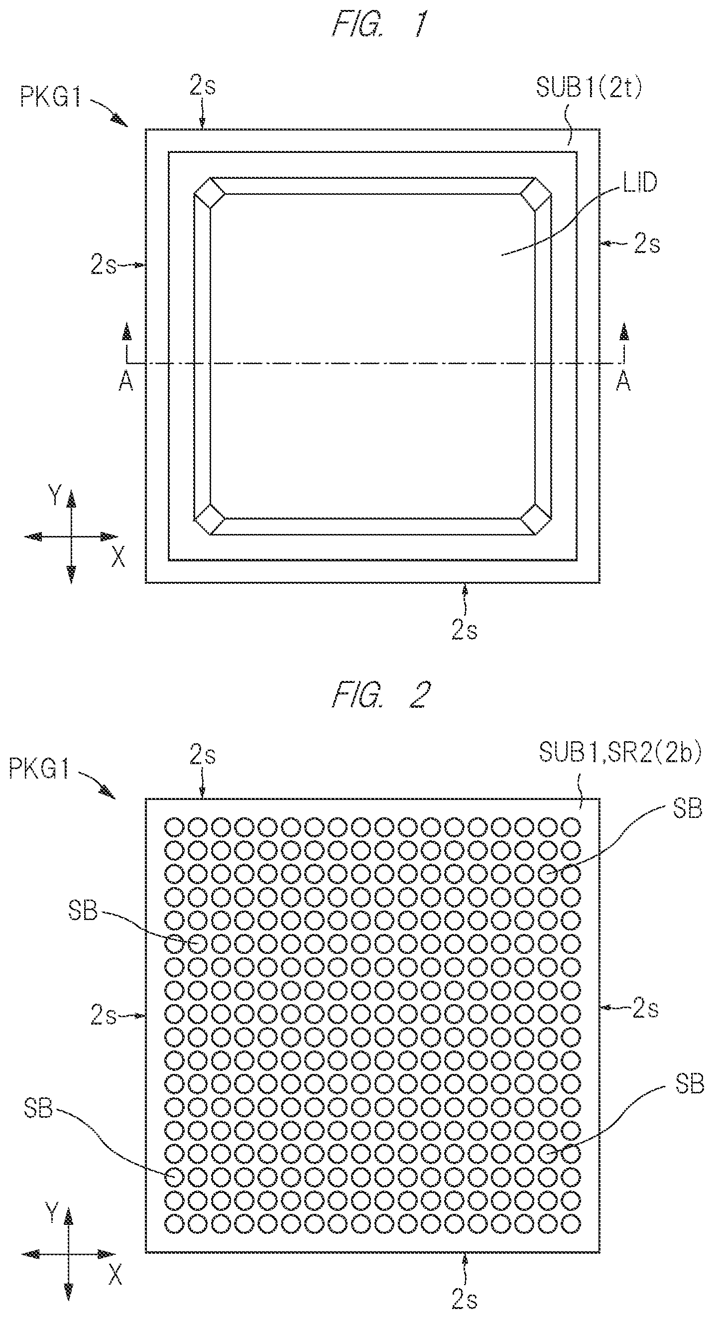
A technique for reducing influence of a noise in a path configured to supply power to a circuit is needed along with higher functionality of a semiconductor device in order to stabilize an operation of the circuit in the semiconductor device. For example, an analog circuit such as phase locked loop (PLL) circuit may be provided in a semiconductor chip in a semiconductor device in order to stabilize a transmission quality of a digital signal. The noise is easier to influence the circuit operation in the analog circuit than a digital circuit, and thus a path configured to supply power to the analog circuit may be preferably shorter in path distance than other paths (such as a path configured to supply power to the digital circuit). However, along with higher functionality of a semiconductor device, the number of external terminals in the semiconductor device tends to increase. An arrangement density of the external terminals tends to increase in order to downsize the semiconductor device. Consequently, some paths between an electrode of a semiconductor chip and the respective external terminal configured to supply power to an analog circuit may be longer in path distance. An electric power supplying path with the long path distance from the electrode of the semiconductor chip to the external terminal has a large inductance component in the electric power supplying path. Thus, a power supply potential or a reference potential flowing in this path easily changes due to the influence of noise. Other problems and novel characteristics will be apparent from the description of the present specification and the drawings. A semiconductor device according to one embodiment includes a wiring substrate including a plurality of wiring layers, and a semiconductor chip including a first analog circuit. A first power supply potential pattern capable of supplying a first power supply potential to the first analog circuit, and a first reference potential pattern capable of supplying a first reference potential to the first analog circuit are electrically connected with the first analog circuit. One of the first power supply potential pattern and the first reference potential pattern is provided in a first wiring layer which is the nearest to a lower surface of the wiring substrate among the wiring layers. Another of the first power supply potential pattern and the first reference potential pattern is provided in a second wiring layer which is the next nearest to the lower surface after the first wiring layer. The first power supply potential pattern and the first reference potential pattern extend in the same direction while mutually overlapping. According to the above-described embodiment, performance of a semiconductor device can be improved. BRIEF DESCRIPTIONS OF THE DRAWINGS is a top view of a semiconductor device according to one embodiment. is a bottom view of the semiconductor device of . is a plan view of an internal structure of the semiconductor device illustrated in on a wiring substrate with a cover member removed. is a cross-section view taken along line A-A of . is an explanatory diagram of an exemplary structure of circuits included in the semiconductor device of . is a schematic explanatory diagram of paths configured to supply power to an analog circuit of . is an enlarged plan view of exemplary noise countermeasures for power supply potential supplying paths and reference potential supply paths illustrated in . is an enlarged cross-section view taken along line B-B of . is an enlarged plan view of another exemplary noise countermeasures for the power supply potential supplying paths and the reference potential supply paths illustrated in . is an enlarged cross-section view taken along line C-C of . is an enlarged plan view of still another exemplary noise countermeasures for the power supply potential supplying paths and the reference potential supply paths illustrated in . is an enlarged cross-section view taken along line D-D of . is an enlarged plan view of only a power supply potential pattern and a reference potential pattern illustrated in is an enlarged plan view of still another exemplary noise countermeasures for the power supply potential supplying paths and the reference potential supply paths illustrated in . is an enlarged plan view of another modification example of . is an enlarged plan view of still another modification example of . is an enlarged plan view of an exemplary shape of a conductor pattern formed in the third wiring layer from the lowermost wiring layer illustrated in . is an enlarged plan view of an exemplary shape of a conductor pattern formed in the third wiring layer ordered from the lowermost wiring layer illustrated in . is a plan view to compare in difference between a width of a signal wiring configured to transmit an electric signal to the analog circuit illustrated in and wiring widths of a reference potential pattern and a power supply potential pattern illustrated in or . is an enlarged cross-section view of a modification example of or .
DETAILED DESCRIPTION
Description of Explanation Form, Basic Terms, and their Use in Present Application In the present application, the invention will be described in a plurality of sections or embodiments when required as a matter of convenience. However, these sections or embodiments are not irrelevant to each other unless otherwise stated. Regardless of before and after the description, one part of a simple example is a detailed part, a part, or the entire of a modification example of the other. Also, in principle, the repetitive description of the same part is omitted. Further, each element in the embodiment is not indispensable unless otherwise particularly stated not to be so, logically limited to the number, and clearly not to be so from the contexts. Similarly, when a material, a composition or others is described as “X made of A” or others in the description of the embodiments or others, the one containing other components than A is not excluded unless otherwise stated not to be so and clearly not being so from the contexts. For example, the component means “X containing A as a main component” or others. For example, the component means “X containing A as a main component” or others. For example, it is needless to say that a “silicon material” and others includes not only pure silicon but also SiGe (silicon germanium) alloy or other multicomponent alloy containing silicon as a main component, or a material containing other additives or others. Also, gold plating, a Cu layer, nickel plating, and others include not only pure material but also members containing gold, Cu, nickel, and others as a main component, respectively, unless otherwise specified not to be so. Further, even when a specific numerical value and numerical amount are mentioned, the specific numerical value and the numerical amount may exceed the specific numerical values or smaller than the specific numerical values unless otherwise specified not to be so, logically limited to the number, and clearly not being so from the contents. Still further, in each drawing of the embodiment, the same or similar parts are denoted by the same or similar symbol or reference number, and the description thereof is not repeated in principle. Also, in the attached drawings, hatching or others is omitted even in a cross-sectional view in some cases such as a case of causing complication or a case of clearly distinguishing a portion from a space. In respect to this, a background outline is omitted even in a closed hole in a plan view when being clear from the explanation or others. Further, hatching or a dot pattern is added to a drawing in some cases in order to clearly show that the portion is not the space or clearly show a boundary between regions even if the drawing is not a cross-sectional view. “Semiconductor component” in the present specification is a component utilizing electron in a semiconductor. As examples of the “semiconductor component”, a semiconductor chip and a semiconductor device packaging a semiconductor chip therein can be exemplified. Regardless of whether to include the semiconductor, a component which is embedded in an electric circuit and has an electric function is called “electronic component.” Examples of the electronic component include not only the semiconductor component but also a resister element, a capacitor element, an inductor element and others. Semiconductor Device is a top view of a semiconductor device according to one embodiment. is a bottom view of the semiconductor device of . is a plan view of an internal structure of the semiconductor device illustrated in on a wiring substrate with a cover member removed. is a cross-section view taken along line A-A of . A semiconductor device PKG 1 according to the present embodiment includes a wiring substrate SUB 1 , and a semiconductor chip CHP 1 (see ) mounted on the wiring substrate SUB 1 . The semiconductor device PKG 1 includes a bond layer BND 1 arranged on the semiconductor chip CHP 1 , and a cover member LID configured to cover the entire semiconductor chip CHP 1 , the entire bond layer BND 1 , and part of the wiring substrate SUB 1 , and fixed with the bond layer BND 1 . As illustrated in , the wiring substrate SUB 1 has an upper surface (surface, main surface, chip mounting surface, first main surface) 2 t mounting the semiconductor chip CHP 1 thereon and a lower surface (surface, main surface, mounting surface, second main surface) 2 b opposite the upper surface 2 t . The wiring substrate SUB 1 has a plurality of sides 2 s (see to 3 ) configuring the outer edges of the upper surface 2 t and the lower surface 2 b in plan view. In the present embodiment, the upper surface 2 t (see ) and the lower surface 2 b (see ) of the wiring substrate SUB 1 are rectangular, and the wiring substrate SUB 1 has four sides 2 s in plan view. The wiring substrate SUB 1 includes a plurality of (in the example of , eight) wiring layers WL 1 , WL 2 , WL 3 , WL 4 , WL 5 , WL 6 , WL 7 , and WL 8 provided between the upper surface 2 t and the lower surface 2 b . The wiring layers include the wiring layer WL 1 which is the nearest to the upper surface 2 t of the wiring substrate SUB 1 among the plurality of wiring layers and is provided with terminals (terminals 2 PD). The wiring layers further include the wiring layer WL 8 which is the nearest to the lower surface 2 b of the wiring substrate SUB 1 among the plurality of wiring layers and is provided with terminals (lands 2 LD). Each wiring layer has a conductor pattern such as wiring which is a path configured to supply an electric signal or power. An insulative layer 2 e is arranged between the wiring layers. The respective wiring layers are electrically connected to each other through a via 2 v which is an interlayer conductive path penetrating through the insulative layer 2 e or a through-hole wiring 2 THW. In the present embodiment, a wiring substrate including eight wiring layers is illustrated as an example of the wiring substrate SUB 1 , but the number of wiring layers of the wiring substrate SUB 1 is not limited to eight. A wiring substrate including seven or less wiring layers or nine or more wiring layers may be employed in a modification example. The nearest wiring layer WL 1 (the uppermost layer) to the upper surface 2 t among the wiring layers is covered with an insulative film SR 1 . The insulative film SR 1 is provided with openings, and the terminals 2 PD provided on the wiring layer WL 1 are exposed from the insulative film SR 1 at the openings. A plurality of lands is provided on the nearest wiring layer WL 8 (the lowermost wiring layer) to the lower surface 2 b of the wiring substrate SUB 1 among the wiring layers. The wiring layer WL 8 is covered with an insulative film SR 2 . The insulative film SR 1 and the insulative film SR 2 are solder-resist films. The terminals 2 PD provided on the wiring layer WL 1 are electrically connected to the lands (land patterns) 2 LD provided on the wiring layer WL 8 , respectively, through the conductor patterns (wirings 2 d or large-area conductor patterns), the vias 2 v , and the through-hole wirings 2 THW, which are formed on the wiring layers of the wiring substrate SUB 1 . The wiring substrate SUB 1 is formed by, for example, a buildup method of stacking the respective wiring layers on an upper surface 2 Ct and a lower surface 2 Cb of an insulative layer (core material, core insulative layer) 2 CR which is made of prepreg in which resin is immersed in a glass fiber. The wiring layer WL 4 on the side of the upper surface 2 Ct of the insulative layer 2 CR is electrically connected to the wiring layer WL 5 on the side of the lower surface 2 Cb through the plurality of through-hole wirings 2 THW embedded in a plurality of through holes configured to penetrate from one of the upper surface 2 Ct and the lower surface 2 Cb to the other thereof. In the example of , the wiring substrate SUB 1 is described as a wiring substrate in which a plurality of wiring layers is stacked on the sides of the upper surface 2 Ct and the lower surface 2 Cb of the insulative layer 2 CR as a core material. A modification example of employs so-called coreless substrate in which the insulative layers 2 e and the conductor patterns such as the wirings 2 d are sequentially stacked without the insulative layer 2 CR made of a hard material such as prepreg. In the case of use of the coreless substrate, the wiring layers are electrically connected through the vias 2 v without the formation of the through-hole wirings 2 THW. In the example of , solder balls (solder materials, external terminals, electrodes, external electrodes) SB are connected to the lands 2 LD, respectively. The solder balls SB are conductive members configured to electrically connect a plurality of terminals (not illustrated) on the motherboard side with the lands 2 LD when the semiconductor device PKG 1 is mounted on the motherboard (not illustrated). The solder balls SB are made of, for example, a lead (Pb)-containing Sn—Pb solder material or so-called lead-free solder material substantially not containing Pb. Examples of lead-free solder include only tin (Sn), tin-bismuth (Sn—Bi), tin-copper-silver (Sn—Cu—Ag), tin-copper (Sn—Cu), and the like. The lead-free solder described here means a material, a lead (Pb) content of which is 0.1 wt % or less, and the content is defined in accordance with Restriction of Hazardous Substances (RoHS) Directive. A plurality of solder balls SB is arranged in a matrix shape (array shape) as illustrated in . Although not illustrated in , the lands 2 LD (see ) bonded with the solder balls SB are also arranged in a matrix shape (array shape). In this manner, a semiconductor device in which a plurality of external terminals (solder balls SB, lands 2 LD) is arranged in a matrix shape on the mounting surface of the wiring substrate SUB 1 is called area-array-type semiconductor device. In the area-array-type semiconductor device, the mounting surface (lower surface 2 b ) of the wiring substrate SUB 1 is effectively used as an arranging space for the external terminals, and thus this type is preferable in a viewpoint that is suppression of an increase in the mounting area of the semiconductor device even in increase in the number of external terminals. That is, a semiconductor device with the increase in the number of external terminals along with higher functionality and higher integration can be mounted in a small space. The semiconductor device PKG 1 includes the semiconductor chip CHP 1 mounted on the wiring substrate SUB 1 . As illustrated in , each semiconductor chip CHP 1 has a front surface (main surface, upper surface) 3 t and a back surface (main surface, lower surface) 3 b opposite the front surface 3 t . The semiconductor chip CHP 1 has a plurality of sides 3 s configuring the outer edges of the front surface 3 t and the back surface 3 b in plan view. The semiconductor chip CHP 1 is formed in a square outer shape with the smaller plane area than that of the wiring substrate SUB 1 in plan view as illustrated in . Thus, the semiconductor chip CHP 1 has four sides 3 s in plan view. In the example of , the semiconductor chip CHP 1 is mounted at the center of the upper surface 2 t of the wiring substrate SUB 1 , and the four sides 3 s of the semiconductor chip CHP 1 extend along the four sides 2 s of the wiring substrate SUB 1 , respectively. A plurality of electrodes (pads, electrode pads, bonding pads) 3 PD is formed on the upper surface 3 t side of the semiconductor chip CHP 1 . In the example of , the semiconductor chip CHP 1 is mounted on the wiring substrate SUB 1 in a state in which the upper surface 3 t faces the upper surface 2 t of the wiring substrate SUB 1 . Such a mounting method is called face-down mounting method or flip-chip connecting method. Although not illustrated, a plurality of semiconductor elements (circuit elements) is formed on the main surface of the semiconductor CHP 1 (more specifically, a semiconductor element forming region provided on an element forming surface of a semiconductor substrate that is a base member of the semiconductor chip CHP 1 ). The plurality of electrodes 3 PD is electrically connected to the plurality of semiconductor elements, respectively, through the wirings (not illustrated) formed on a wiring layer arranged inside the semiconductor chip CHP 1 (more specifically, between the upper surface 3 t and a semiconductor element forming region not illustrated). The semiconductor substrate provided in the semiconductor chip CHP 1 is made of, for example, silicon (Si). An insulative film covering the semiconductor substrate and the wirings is formed on the upper surface 3 t of the semiconductor chip CHP 1 , and part of each electrode 3 PD (see ) is exposed from the insulative film at an opening formed in the insulative film. The electrodes 3 PD are made of a metal, and are made of, for example, aluminum (Al) in the present embodiment. As illustrated in , the electrodes 3 PD are connected with bump electrodes 3 BP, respectively, and the electrodes 3 PD of the semiconductor chip CHP 1 are electrically connected to the terminals 2 PD of the wiring substrate SUB 1 via the bump electrodes 3 BP, respectively. The bump electrodes 3 BP are metal members (conductive members) formed to protrude above the from surface 3 t of the semiconductor chip CHP 1 . The bump electrodes 3 BP in the present embodiment are so-called solder bumps in which a solder material is stacked above an electrode 3 PD via an underlying metal film (under bump metal). The lead-containing solder material or the lead-free solder may be used as the solder material making the solder bumps as similar to the solder balls SB. When the semiconductor chip CHP 1 is mounted on the wiring substrate SUB 1 , a heating processing (reflow processing) is performed while the solder bumps that are previously formed on both of the electrodes 3 PD and the terminals 2 PD are contacted with each other, and thus the solder bumps are unified to form the bump electrodes 3 BP. In a modification example of the present embodiment, pillar bumps in which a solder film is formed on a tip surface of a conductor pillar made of copper (Cu) or nickel (Ni) may be used as the bump electrodes 3 BP. Underfill resin (insulative resin) UF is arranged between the semiconductor chip CHP 1 and the wiring substrate SUB 1 as illustrated in . The underfill resin UF is arranged to close a space between the front surface 3 t of the semiconductor chip CHP 1 and the upper surface 2 t of the wiring substrate SUB 1 . The bump electrodes 3 BP are sealed by the underfill resin UF. The underfill resin UF is made of an insulative (non-conductive) material (such as resin material) and is arranged to seal the electric connections (bonding parts of the bump electrodes 3 BP) between the semiconductor chip CHP 1 and the wiring substrate SUB 1 . In this manner, when the bonding parts between the bump electrodes 3 BP and the terminals 2 PD are covered with the underfill resin UF, stress caused at the electric connections between the semiconductor chip CHP 1 and the wiring substrate SUB 1 can be reduced. The stress caused at the bonding parts between the electrodes 3 PD of the semiconductor chip CHP 1 and the bump electrodes 3 BP can be also reduced. Further, the main surface of the semiconductor chip CHP 1 , on which the semiconductor elements (circuit elements) are formed, can be protected. The cover member (lid, heat spreader, heat radiating member) LID is arranged on the back surface 3 b of the semiconductor chip CHP 1 . The cover member LID is, for example, a metal plate with a higher heat conductivity than that of the wiring substrate SUB 1 , and has a function to discharge heat caused in the semiconductor chip CHP 1 to the outside. The cover member LID is thermally connected to the semiconductor chip CHP 1 via the bond layer BND 1 . The bond layer BND 1 contacts with the semiconductor chip CHP 1 and the cover member LID. The bond layer BND 1 is made of an adhesive obtained by, for example, hardening a paste that is mixed with a filler in a resin paste. As examples of the filler, metallic particles and metallic oxide particles such as alumina can be exemplified. The bond layer BND 1 contains a filler which is mixed to improve the heat radiation property, and thus can improve the heat conductivity between the semiconductor chip CHP 1 and the cover member LID as compared with filler-free resin adhesives. A peripheral region of the cover member LID is adhered and fixed to the upper surface 2 t of the wiring substrate SUB 1 via a bond layer BND 2 . The bond layer BND 2 does not need the heat radiation property as different from the bond layer BND 1 , and thus its material is not particularly limited, and can be optionally selected as long as the material has a necessary adhesive strength. For example, when the same material as that of the bond layer BND 1 is used, its manufacturing steps can be simplified. Alternatively, for example, a material with a higher adhesive strength than that of the bond layer BND 1 may be used. A semiconductor device attached with the cover member LID functioning as a heat radiating member as similar to the semiconductor device PKG 1 can stably operate the circuits therein even in the case of higher functionality because of having a high heat radiation efficiency of the semiconductor chip CHP 1 . In a modification example of the present embodiment, a structure of the wiring substrate SUB 1 described later may be applied to a semiconductor device without the cover member LID, the bond layer BND 1 and the bond layer BND 2 illustrated in . Exemplary Circuit Structure Next, an exemplary structure of circuits provided in the semiconductor device PKG 1 of will be described. is an explanatory diagram of an exemplary structure of circuits provided in the semiconductor device PKG 1 of . Note that some of a plurality of circuits, some of a plurality of signal transmission paths and some of a plurality of power supply paths provided in the semiconductor device PKG 1 are illustrated in as example. As illustrated in , the semiconductor chip CHP 1 of the semiconductor device PKG 1 according to the present embodiment includes an analog circuit AC 1 . In the example of , the semiconductor chip CHP 1 includes the analog circuit AC 1 , and a core circuit CC 1 electrically coupled to the analog circuit AC 1 . The analog circuit AC 1 is, for example, a PLL circuit configured to generate a new signal synchronized with a phase of an input signal. In the example of , a signal (alternate-current signal, high-frequency signal) SG 1 is input from an external device of the semiconductor device PKG 1 into the analog circuit AC 1 . The signal SG 1 is input into the analog circuit AC 1 of the semiconductor chip CHP 1 via a signal transmission path PSG 1 of the wiring substrate SUB 1 . The analog circuit AC 1 includes a phase comparator, a filter circuit and an oscillator not illustrated, and outputs a new signal (alternate-current signal, high-frequency signal) SG 2 synchronized with a phase of the signal SG 1 and a phase of a comparison-target input signal not illustrated. The signal SG 2 is input into the core circuit CC 1 . The core circuit CC 1 performs a data processing (such as operation processing) to the input signal SG 2 , and outputs a signal (alternate-current signal, high-frequency signal) SG 3 . The signal SG 3 is output from the core circuit CC 1 of the semiconductor chip CHP 1 to an external device not illustrated via a signal transmission path PSG 3 of the wiring substrate SUB 1 . By the analog circuit AC 1 that is the PLL circuit, the synchronization processing is performed to the signal SG 2 to be input into the core circuit CC 1 . Thus, the signal SG 2 with less phase fluctuation (jitter) is supplied to the core circuit CC 1 . The core circuit CC 1 is, for example, a digital circuit, but may be an analog circuit. The semiconductor chip CHP 1 includes a power circuit AC 2 configured to supply (capable of supplying) power to the analog circuit AC 1 and a power circuit CC 2 configured to supply (capable of supplying) power to the core circuit CC 1 . A power supply potential VD 1 and a reference potential VS 1 are supplied to the analog circuit AC 1 via the power circuit AC 2 . On the other hand, a power supply potential VD 2 and a reference potential VS 2 are supplied to the core circuit CC 1 via the power circuit CC 2 . The power supply potential VD 1 is supplied to the power circuit AC 2 of the semiconductor chip CHP 1 via a power supply potential supplying path PVD 1 of the wiring substrate SUB 1 . The reference potential VS 1 is supplied to the power circuit AC 2 of the semiconductor chip CHP 1 via a reference potential supplying path PVS 1 of the wiring substrate SUB 1 . The power supply potential VD 2 is supplied to the power circuit CC 2 of the semiconductor chip CHP 1 via a power supply potential supplying path PVD 2 of the wiring substrate SUB 1 . The reference potential VS 2 is supplied to the power circuit CC 2 of the semiconductor chip CHP 1 via a reference potential supply path PVS 2 of the wiring substrate SUB 1 . Note that the reference potential VS 1 is different from the power supply potential VD 1 , and may be a potential other than a ground potential. Similarly, the reference potential VS 2 is different from the power supply potential VD 2 , and may be a potential other than a ground potential. The reference potential VS 1 may be the same as or different from the reference potential VS 2 . As described later, in the present embodiment, even if the reference potential VS 1 is the same as the reference potential VS 2 , the reference potential supply path PVS 1 and the reference potential supply path PVS 2 are configured of mutually separated wiring patterns. In order to stably operate the analog circuit AC 1 of , it is necessary to reduce a change in potential difference between the power supply potential VD 1 and the reference potential VS 1 supplied to the analog circuit AC 1 via the power circuit AC 2 . This is because the change in potential difference between the power supply potential VD 1 and the reference potential VS 1 reduces the quality of the signal SG 2 output from the analog circuit AC 1 . The followings may be exemplified as noise sources influencing the change in potential difference between the power supply potential VD 1 and the reference potential VS 1 . For example, noise induced by the signal SG 1 or the signal SG 3 as a high-frequency signal may influence the potential difference between the power supply potential VD 1 and the reference potential VS 1 . Further, for example, the power supply potential VD 2 may be instantaneously changed by influence of a power demand of the core circuit CC 1 . At this time, if the power supply potential supplying path PVD 2 is arranged near the power supply potential supplying path PVD 1 and the reference potential supply path PVS 1 , noise caused in the power supply potential VD 2 may influence the potential difference between the power supply potential VD 1 and the reference potential VS 1 . In order to reduce the influence of noise on the potential difference between the power supply potential VD 1 and the reference potential VS 1 , it is preferable to shorten the path distances of the power supply potential supplying path PVD 1 and the reference potential supply path PVS 1 . The shortened path distances enable inductance of the power supply potential supplying path PVD 1 and the reference potential supply path PVS 1 to be reduced, and thus the influence of noise is reduced. However, the number of external terminals of each semiconductor device tends to increase along with higher functionality of the semiconductor device. Further, an arrangement density of a plurality of external terminals tends to be high in order to downsize the semiconductor device. The power supply potential supplying path PVD 1 and the reference potential supply path PVS 1 may be inevitably longer. In other words, if the influence of noise can be reduced even when the path distances of the power supply potential supplying path PVD 1 and the reference potential supply path PVS 1 are long, a degree of freedom for design can be improved. A next section explains a technique for reducing the influence of noise by developing the layout of the power supply potential supplying path PVD 1 and the reference potential supply path PVS 1 in the wiring substrate SUB 1 . Layout of Power Supply Paths is a schematic explanatory diagram of the paths configured to supply power to the analog circuits of . A contour of a region R 1 overlapping with the semiconductor chip CHP 1 is illustrated with a dotted line in . The semiconductor device PKG 1 includes a plurality of pairs of the power supply potential supplying paths PVD 1 and the reference potential supply paths PVS 1 as illustrated in . The power supply potential supplying paths PVD 1 and the reference potential supply paths PVS 1 are arranged in pairs. The bump electrodes 3 BP are arranged within the region R 1 overlapping with the semiconductor chip CHP 1 . Lands 2 LD, which are included in either the power supply potential supplying paths PVD 1 or the reference potential supply paths PVS 1 , among the lands 2 LD are arranged outside the region R 1 in plan view. The lands included in the power supply potential supplying path PVD 2 and the reference potential supply path PVS 2 , which are configured to mainly supply power to the core circuit CC 1 of , are arranged in the region R 1 (particularly the region overlapping with the core circuit CC 1 of ). Thus, it is difficult in the region R 1 to secure a space for arranging the lands 2 LD included in either the power supply potential supplying paths PVD 1 or the reference potential supply paths PVS 1 . Note that some of the lands 2 LD included in either the power supply potential supplying paths PVD 1 or the reference potential supply paths PVS 1 may be arranged within the region R 1 . The bump electrodes 3 BP and the lands 2 LD, which are electrically connected to each other, are preferably arranged near each other in transparent plan view. However, the lands 2 LD may be difficult to be arranged near the bump electrodes 3 BP depending on a design condition. The example of shows a power supply potential supplying path PVD 1 S and a reference potential supply path PVS 1 S whose path distances connecting the bump electrodes 3 BP and the lands 2 LD are relatively short, and a power supply potential supplying path PVD 1 L and a reference potential supply path PVS 1 L whose path distances connecting the bump electrodes 3 BP and the lands 2 LD are relatively long. further illustrates a power supply potential supplying path PVD 1 M and a reference potential supply path PVS 1 M whose path distances connecting the bump electrodes 3 BP and the lands 2 LD are relatively medium. The path distances of the power supply potential supplying path PVD 1 S and the reference potential supply path PVS 1 S (a path distance DVDS and a path distance DVSS between the bump electrodes 3 BP and the lands 2 LD) are, for example, 5 mm or less. The path distances of the power supply potential supplying path PVD 1 M and the reference potential supply path PVS 1 M (a path distance DVDM and a path distance DVSM between the bump electrodes 3 BP and the lands 2 LD) are, for example, more than 5 mm and 7 mm or less. The path distances of the power supply potential supplying path PVD 1 L and the reference potential supply path PVS 1 L (a path distance DVDL and a path distance DVSL between the bump electrodes 3 BP and the lands 2 LD) are, for example, more than 7 mm. The path distances of the power supply potential supplying path PVD 1 L and the reference potential supply path PVS 1 L may be 10 mm or more. The relations among the path distances illustrated in may be expressed as follows. The path distance of the power supply potential supplying path PVD 1 L including a power supply potential pattern LVD 1 (see described later) between a bump electrode 3 BP of the semiconductor chip CHP 1 (see ) and a land 2 LD of the wiring substrate SUB 1 is assumed as path distance DVDL. The path distance of the reference potential supply path PVS 1 L including a reference potential pattern LVS 1 (see described later) between a bump electrode 3 BP of the semiconductor chip CHP 1 and a land 2 LD of the wiring substrate SUB 1 is assumed as path distance DVSL. The path distance of the power supply potential supplying path PVD 1 S including a power supply potential pattern LVD 3 (see described later) between a bump electrode 3 BP of the semiconductor chip CHP 1 and a land 2 LD of the wiring substrate SUB 1 is assumed as path distance DVDS. The path distance of the reference potential supply path PVS 1 S including a reference potential pattern LVS 3 (see described later) between a bump electrode 3 BP of the semiconductor chip CHP 1 and a land 2 LD of the wiring substrate SUB 1 is assumed as path distance DVSS. The path distance of the power supply potential supplying path PVD 1 M including a power supply potential pattern LVD 4 (see described later) between a bump electrode 3 BP of the semiconductor chip CHP 1 (see ) and a land 2 LD of the wiring substrate SUB 1 is assumed as path distance DVDM. The path distance of the reference potential supply path PVS 1 M including a reference potential pattern LVS 4 (see described later) between a bump electrode 3 BP of the semiconductor chip CHP 1 and a land 2 LD of the wiring substrate SUB 1 is assumed as path distance DVSM. In this case, the path distance DVDL is longer than the path distance DVDM, the path distance DVDS, the path distance DVSM, and the path distance DVSS. The path distance DVSL is longer than the path distance DVDM, the path distance DVDS, the path distance DVSM, and the path distance DVSS. The path distance DVDM is longer than the path distance DVDS and the path distance DVSS. The path distance DVSM is longer than the path distance DVDS and the path distance DVSS. In the example of , in particular, noise countermeasures need to be preferentially applied to the power supply potential supplying path PVD 1 L and the reference potential supply path PVS 1 L. Noise countermeasures need to be preferentially applied to the power supply potential supplying path PVD 1 M and the reference potential supply path PVS 1 M over the power supply potential supplying path PVD 1 S and the reference potential supply path PVS 1 S. Noise countermeasures will be described in details below. First Noise Countermeasure Noise countermeasures effectively applicable to the power supply potential supplying path PVD 1 S and the reference potential supply path PVS 1 S illustrated in will be first described as first noise countermeasures. is an enlarged plan view of exemplary noise countermeasures for the power supply potential supplying paths and the reference potential supply paths illustrated in . is an enlarged cross-section view taken along line B-B of . Symbols in are given to schematically show an inductive coupling state between the power supply potential pattern LVD 3 configuring the power supply potential supplying path PVD 1 and the reference potential pattern LVS 3 configuring the reference potential supply path PVS 1 . The wiring layer illustrated in among the wiring layers illustrated in is, for example, a wiring layer WL 7 . The wiring layer WL 7 among the wiring layers is the next nearest to the lower surface 2 b of the wiring substrate SUB 1 after the wiring layer WL 8 as illustrated in . Although not illustrated, the power supply potential pattern LVD 3 and the reference potential pattern LVS 3 as similar to those in in a modification example may be arranged in the wiring layers other than the wiring layer WL 7 . A method of inductively coupling the power supply potential pattern LVD 3 and the reference potential pattern LVS 3 is effective as a method of reducing the influence of noise on the power supply potential supplying path PVD 1 and the reference potential supply path PVS 1 illustrated in . Inductive coupling means a state in which mutual induction between a power supply potential supplying path and a reference potential supply path dominantly works. When a power supply potential supplying path and a reference potential supply path are inductively coupled, loop inductance between the paths can be reduced by mutual induction. Consequently, a variation in voltage with respect to high-frequency current components can be suppressed (in other words, self-noise can be reduced). For example, when high-frequency noise or pulse noise is on the power supply potential pattern LVD 3 to which a fixed potential is supplied, if the power supply potential pattern LVD 3 and the reference potential pattern LVS 3 are inductively coupled, a variation in potential with respect to high-frequency current components flowing in the loop path can be suppressed. The power supply potential pattern LVD 3 and the reference potential pattern LVS 3 are formed in the same wiring layer WL 7 as illustrated in . The power supply potential pattern LVD 3 and the reference potential pattern LVS 3 extend in the same direction while being mutually adjacent in plan view. The power supply potential pattern LVD 3 and the reference potential pattern LVS 3 are inductively coupled as schematically illustrated with capacitor circuit symbols in . Effects of the noise countermeasures using inductively coupling the power supply potential pattern LVD 3 and the reference potential pattern LVS 3 are proportional to a magnitude of mutual inductance between the power supply potential pattern LVD 3 and the reference potential pattern LVS 3 . Thus, the larger a facing path width of the power supply potential pattern LVD 3 and the reference potential pattern LVS 3 facing each other via the insulative layer 2 e is, and besides, the smaller a separation distance between the facing patterns is, the more the noise countermeasure effect is. Note that the facing path width means a width of a part at which the power supply potential supplying path and the reference potential supply path face each other. In the example of , each thickness (each length in the Z direction of ) of the power supply potential pattern LVD 3 and the reference potential pattern LVS 3 corresponds to the facing path width. Thus, in the example of , the thicknesses of the power supply potential pattern LVD 3 and the reference potential pattern LVS 3 , which are in parallel with each other, are preferably larger, and the separation distance between the power supply potential pattern LVD 3 and the reference potential pattern LVS 3 are preferably shorter. Conductor patterns 2 CP are arranged adjacent to the power supply potential pattern LVD 3 and the reference potential pattern LVS 3 , respectively, in plan view of . The conductor patterns 2 CP are paths through which any potential is supplied. For example, the conductor pattern 2 CP configures either the power supply potential supplying path PVD 2 or the reference potential supply path PVS 2 described in . Alternatively, the conductor pattern 2 CP illustrated in may configure other potential supply path not illustrated. The wiring substrate SUB 1 includes a reference potential pattern LVS 2 (see ) capable of supplying the reference potential VS 2 to a circuit (such as the core circuit CC 1 of ) other than the analog circuit AC 1 of . The reference potential pattern LVS 2 is a conductor pattern configuring part of the reference potential supply path PVS 2 of . As illustrated in , the reference potential patterns LVS 2 are formed in the wiring layer WL 6 and the wiring layer WL 8 which are adjacent to the wiring layer WL 7 where a power supply potential pattern LVD 3 and a reference potential pattern LVS 3 are formed, among the wiring layers of the wiring substrate SUB 1 , and overlap with the power supply potential pattern LVD 3 and the reference potential pattern LVS 3 . The reference potential patterns LVS 2 in the wiring layer WL 6 and the wiring layer WL 8 preferably extend in the same direction while overlapping with the power supply potential pattern LVD 3 and the reference potential pattern LVS 3 . The reference potential pattern LVS 2 functions as an electromagnetic shield configured to suppress surrounding noise from reaching the power supply potential pattern LVD 3 and the reference potential pattern LVS 3 . When the reference potential pattern LVS 2 functioning as an electromagnetic shield is provided as illustrated in , noise applied to the power supply potential pattern LVD 3 and the reference potential pattern LVS 3 can be reduced. The example of shows the embodiment in which the power supply potential pattern LVD 3 and the reference potential pattern LVS 3 are formed in the wiring layer WL 7 , and thus the reference potential patterns LVS 2 functioning as electromagnetic shields are arranged in the wiring layer WL 6 and the wiring layer WL 8 . In a modification example, the power supply potential pattern LVD 3 and the reference potential pattern LVS 3 may be formed in the wiring layer WL 8 . In this case, if the reference potential pattern LVS 2 is arranged in the wiring layer WL 7 , the structure of the wiring layer WL 6 is not particularly limited. In the method illustrated in , the thicknesses of the power supply potential pattern LVD 3 and the reference potential pattern LVS 3 are difficult to remarkably increase. The thicknesses of the power supply potential pattern LVD 3 and the reference potential pattern LVS 3 illustrated in are, for example, about 10 to 20 μm. Thus, an upper limit of mutual induction between the power supply potential pattern LVD 3 and the reference potential pattern LVS 3 is low. Therefore, the method illustrated in is of limited effectiveness for the noise countermeasures on, for example, the paths with a long distance and large path inductance such as the power supply potential supplying path PVD 1 M or the power supply potential supplying path PVD 1 L of . As described above, the power supply potential supplying path PVD 1 S and the reference potential supply path PVS 1 S illustrated in have the path distance DVDS and the path distance DVSS of 5 mm or less, respectively, and have small path inductance (have smaller path inductance than, for example, that of the power supply potential supplying path PVD 1 M or the power supply potential supplying path PVD 1 L). Thus, the case of the power supply potential pattern LVD 3 and the reference potential pattern LVS 3 can reduce the noise even when the power supply potential pattern LVD 3 and the reference potential pattern LVS 3 are formed in the same wiring layer WL 7 as illustrated in . Second Noise Countermeasures Noise countermeasure technique effectively applicable to the power supply potential supplying path PVD 1 M and the power supply potential supplying path PVD 1 L illustrated in will be described below as second noise countermeasures. The second noise countermeasures and third noise countermeasures will be described below in assumption that at least one of the power supply potential pattern LVD 1 and the reference potential pattern LVS 1 is arranged in the lowermost wiring layer WL 8 . A method of adding a new wiring layer for noise countermeasures in addition to the wiring layers WL 1 to WL 8 of is also considerable. However, an increase in the number of wiring layers causes demerits such as an increase in the thickness of the semiconductor device, an increase in the steps of manufacturing the wiring substrate, or an increase in manufacturing cost due to an increase in the number of materials for making the wiring substrate. Thus, the present inventors have studied a technique for reducing noise by use of the lowermost wiring layer WL 8 without adding the wiring layer for noise countermeasures. is an enlarged plan view of another exemplary noise countermeasures for the power supply potential supplying paths and the reference potential supply paths illustrated in . is an enlarged cross-section view taken along line C-C of . In the exemplary noise countermeasures illustrated in , the power supply potential pattern LVD 1 and the reference potential pattern LVS 1 are separately arranged in adjacent wiring layers. If illustrations of the wiring layer WL 7 and the wiring layer WL 8 of overlap with each other, the power supply potential pattern LVD 4 and the reference potential pattern LVS 4 are difficult to distinguish from each other. Thus, needs to illustrate the wiring layer WL 7 and the wiring layer WL 8 in transparent plan view, but illustrates part of the wiring layer WL 7 and part of the wiring layer WL 8 overlapping therewith to be vertically arranged. accurately illustrates positional relation among the power supply potential pattern LVD 4 , the reference potential pattern LVS 4 , and the lands 2 LD in transparent plan view when the wiring substrate SUB 1 is viewed from the lower surface 2 b (see ), and can be regarded as a transparent plan view. Each of , 14 , 15 , and 16 described later is also a diagram illustrating part of the wiring layer WL 7 and part of the wiring layer WL 8 overlapping therewith to be vertically arranged as similar to , and each of these drawings can be regarded as transparent plan view. Each of described later is a diagram illustrating part of the wiring layer WL 6 , part of the wiring layer WL 7 overlapping therewith, and part of the wiring layer WL 8 overlapping therewith to be vertically arranged as similar to , and each of these drawings can be regarded as transparent plan view. Symbols in are given to schematically illustrate a state in which the power supply potential pattern LVD 4 and the reference potential pattern LVS 4 are inductively coupled. The analog circuit AC 1 of is electrically connected with the power supply potential pattern LVD 4 (see ) capable of supplying the power supply potential VD 1 to the analog circuit AC 1 and the reference potential pattern LVS 4 (see ) capable of supplying the reference potential VS 1 to the analog circuit AC 1 . The power supply potential pattern LVD 4 illustrated in configures part of the power supply potential supplying path PVD 1 M of . The reference potential pattern LVS 4 configures part of the reference potential supply path PVS 1 M of . As illustrated in , one of the power supply potential pattern LVD 4 and the reference potential pattern LVS 4 is provided in the wiring layer WL 8 , and another thereof is provided in the wiring layer WL 7 . Note that the example of shows that the power supply potential pattern LVD 4 is provided in the wiring layer WL 8 while the reference potential pattern LVS 4 is provided in the wiring layer WL 7 . However, in a modification example, the reference potential pattern LVS 4 may be provided in the wiring layer WL 8 while the power supply potential pattern LVD 4 may be provided in the wiring layer WL 7 . The power supply potential pattern LVD 4 and the reference potential pattern LVS 4 extend in the same direction while mutually overlapping in transparent plan view. One pattern (that is the power supply potential pattern LVD 4 in ) of the power supply potential pattern LVD 4 and the reference potential pattern LVS 4 , the pattern being arranged in the wiring layer WL 8 , is formed to extend with a width WV 4 . Another pattern (that is the reference potential pattern LVS 4 in ) being arranged in the wiring layer WL 7 is similarly formed to extend with a width WV 4 . In the case of the noise countermeasures of , the power supply potential pattern LVD 4 and the reference potential pattern LVS 4 face each other via the insulative layer 2 e functioning as a dielectric body in the thickness direction of the wiring substrate SUB 1 (in the Z direction in ). Thus, the area of the facing part of the power supply potential pattern LVD 4 and the reference potential pattern LVS 4 can be made larger than in the example of . In the example of , the width WV 4 is, for example, about 50 to 200 μm, and is larger than a thickness TV 4 (for example, about 10 to 20 μm) of the power supply potential pattern LVD 4 and the reference potential pattern LVS 4 illustrated in . Therefore, mutual induction between the power supply potential pattern LVD 4 and the reference potential pattern LVS 4 is larger than mutual induction between the power supply potential pattern LVD 3 and the reference potential pattern LVS 3 illustrated in . The thickness of the power supply potential pattern LVD 1 and the reference potential pattern LVS 1 illustrated in to 16 , 18 , and 19 described later is also, for example, about 10 to 20 μm as similar to the thickness TV 4 of the power supply potential pattern LVD 4 and the reference potential pattern LVS 4 illustrated in . The configuration of is effectively applicable particularly to the power supply potential supplying paths with a longer path distance such as the power supply potential supplying path PVD 1 M or the power supply potential supplying path PVD 1 L illustrated in . A configuration of described later is more effective to the power supply potential supplying path PVD 1 L of . In the example of , in the wiring layer WL 8 , the power supply potential pattern LVD 4 is arranged between two adjacent lands 2 LD among the lands 2 LD in the Y direction crossing with (orthogonal to, in ) a direction in which the power supply potential pattern LVD 4 extends (in the X direction in ). The width WV 4 is smaller than a center-to-center distance PLD between adjacent lands 2 LD in the Y direction and is smaller than a separation distance GLD. Third Noise Countermeasures Next, noise countermeasure technique particularly effectively applicable to the power supply potential supplying path PVD 1 L illustrated in will be described below as third noise countermeasures. is an enlarged plan view of still another exemplary noise countermeasures for the power supply potential supplying paths and the reference potential supply paths illustrated in . is an enlarged cross-section view taken along line D-D of . is an enlarged plan view of only the power supply potential pattern and the reference potential pattern illustrated in . In the exemplary noise countermeasures illustrated in to 13 , the power supply potential pattern LVD 1 and the reference potential pattern LVS 1 are separately arranged in adjacent wiring layers. Thus, illustrates part of the wiring layer WL 7 and part of the wiring layer WL 8 overlapping therewith to be vertically arranged, as similar to . Symbols in are given to schematically illustrate a state in which the power supply potential pattern LVD 1 and the reference potential pattern LVS 1 are inductively coupled. The analog circuit AC 1 of is electrically connected with the power supply potential pattern LVD 1 (see ) capable of supplying the power supply potential VD 1 to the analog circuit AC 1 and the reference potential pattern LVS 1 (see ) capable of supplying the reference potential VS 1 to the analog circuit AC 1 . The power supply potential pattern LVD 1 illustrated in configures part of the power supply potential supplying path PVD 1 L of . The reference potential pattern LVS 1 configures part of the reference potential supply path PVS 1 L of . As illustrated in , one of the power supply potential pattern LVD 1 and the reference potential pattern LVS 1 is provided in the wiring layer WL 8 , and another thereof is provided in the wiring layer WL 7 . Note that the example of shows that the power supply potential pattern LVD 1 is provided in the wiring layer WL 8 while the reference potential pattern LVS 1 is provided in the wiring layer WL 7 . However, in a modification example, the reference potential pattern LVS 1 may be provided in the wiring layer WL 8 while the power supply potential pattern LVD 1 may be provided in the wiring layer WL 7 . As illustrated in , one of the power supply potential pattern LVD 1 and the reference potential pattern LVS 1 is provided in the wiring layer WL 8 and another thereof is provided in the wiring layer WL 7 . The example of illustrates that the power supply potential pattern LVD 1 is provided in the wiring layer WL 8 and the reference potential pattern LVS 1 is provided in the wiring layer WL 7 , but in a modification example, the reference potential pattern LVS 1 may be provided in the wiring layer WL 8 and the power supply potential pattern LVD 1 may be provided in the wiring layer WL 7 . As illustrated in , one pattern (the power supply potential pattern LVD 1 in the example of ) of the power supply potential pattern LVD 1 and the reference potential pattern LVS 1 , the pattern being arranged in the wiring layer WL 8 , has a planar shape extending along the outer edges of the lands 2 LD arranged adjacent to the power supply potential pattern LVD 1 among the lands 2 LD. The power supply potential pattern LVD 1 includes a plurality of wide parts LWD 1 (see ) with a width WV 1 W in the Y direction crossing with (orthogonal to, in ) a direction in which the power supply potential pattern LVD 1 extends (in the X direction in ), and a plurality of narrow parts LND 1 (see ) with a width WV 1 N smaller than the width WV 1 W in the Y direction. As illustrated in , the wide parts LWD 1 and the narrow parts LND 1 are alternately arranged in the direction (the X direction) in which the power supply potential pattern LVD 1 extends. As illustrated in , the width WV 1 W is larger than the separation distance GLD between adjacent lands 2 LD via the power supply potential pattern LVD 1 in the Y direction. The narrow parts LND 1 (see ) and the wide parts LWD 1 (see ) overlap with one pattern (the reference potential pattern LVS 1 in the example of ) of the power supply potential pattern LVD 1 and the reference potential pattern LVS 1 , the one pattern being arranged in the wiring layer WL 7 . As illustrated in , in the case of the third noise countermeasures, by the existence of the wide parts LWD 1 , the area of the facing part of the power supply potential pattern LVD 1 and the reference potential pattern LVS 1 can be made larger than that of the second noise countermeasures of . In the example of , the width WV 1 W is, for example, about 200 to 800 μm, and is larger than the width WV 4 of the power supply potential pattern LVD 4 and the reference potential pattern LVS 4 illustrated in . Thus, mutual induction between the power supply potential pattern LVD 1 and the reference potential pattern LVS 1 is much larger than mutual induction between the power supply potential pattern LVD 4 and the reference potential pattern LVS 4 illustrated in . Therefore, even when the third noise countermeasures of to 13 are applied to a path with the path distance DVDL (or path distance DVSL) of 7 mm or more such as the power supply potential supplying path PVD 1 L or the reference potential supply path PVS 1 L illustrated in , the influence of noise on the power supply potential supplying path PVD 1 L can be reduced. As illustrated as the ranges of the wide parts LWD 1 and the narrow parts LND 1 in , the wide part LWD 1 is defined as a part in the power supply potential pattern LVD 1 which extends with a width WV 1 W that can be substantially regarded to be constant. The width WV 1 W is wider (larger) than the separation distance GLD between adjacent lands 2 LD. In this manner, since the wide parts LWD 1 with the width WV 1 W larger than the separation distance GLD are provided, the third noise countermeasures of can provide higher noise reduction effects than those of the second noise countermeasures of . In the example of , the width WV 1 W is narrower (smaller) than the center-to-center distance PLD between adjacent lands 2 LD in the Y direction. In a modification example described below, the width WV 1 W may be wider (larger) than the center-to-center distance PLD between adjacent lands 2 LD in the Y direction. The narrow part LND 1 is defined as a part with a width smaller than the width WV 1 W. Therefore, the width of the narrow part LND 1 is not always constant as illustrated in . The smallest width WV 1 N in the widths of the narrow parts LND 1 is smaller than the separation distance GLD between adjacent lands of . As illustrated in , the narrow part LND 1 (see ) includes a wider part than the separation distance GLD between adjacent lands 2 LD. A shape of the narrow part LND 1 is determined by a shape of a conductor pattern such as the land 2 LD adjacent to the power supply potential pattern LVD 1 . Therefore, the shape of the narrow part LND 1 of is exemplary, and may be variously modified. However, the power supply potential pattern LVD 1 is arranged to extend between adjacent lands 2 LD in the Y direction, and thus each of the narrow parts LND 1 includes at least a part with a width WV 1 N narrower (smaller) than the separation distance GLD between adjacent lands 2 LD. Next, a shape of the reference potential pattern LVS 1 arranged in the wiring layer WL 7 to face the power supply potential pattern LVD 1 arranged in the wiring layer WL 8 will be described. As illustrated in , in the present embodiment, the power supply potential pattern LVD 1 and the reference potential pattern LVS 1 have a similar planar shape. More specifically, one pattern (the reference potential pattern LVS 1 in the example of ) of the power supply potential pattern LVD 1 and the reference potential pattern LVS 1 , the one pattern being arranged in the wiring layer WL 7 , is formed to imitate a shape of a pattern (the power supply potential pattern LVD 1 in the example of ) formed in the wiring layer WL 8 in transparent plan view. A plurality of wide parts LWS 1 (see ) with the width WV 1 W and a plurality of narrow parts LNS 1 (see ) with a width (such as the width WV 1 N) smaller than the width WV 1 W are provided in the Y direction crossing with (orthogonal to, in ) a direction (X direction) in which the reference potential pattern LVS 1 extends. The wide parts LWS 1 and the narrow parts LNS 1 are alternately arranged in the direction (X direction) in which the reference potential pattern LVS 1 extends. In transparent plan view, the narrow parts LND 1 and the narrow parts LNS 1 overlap with each other, and the wide parts LWD 1 and the wide parts LWS 1 overlap with each other. Note that the definition of the wide part LWS 1 is applicable to the definition of the wide part LWD 1 by replacing the power supply potential pattern LVD 1 with the reference potential pattern LVS 1 . Similarly, the definition of the narrow part LNS 1 is applicable to the definition of narrow part LND 1 by replacing the power supply potential pattern LVD 1 with the reference potential pattern LVS 1 . In this manner, the reference potential pattern LVS 1 and the power supply potential pattern LVD 1 mostly face each other when the planar shape of the reference potential pattern LVS 1 and the planar shape of the power supply potential pattern LVD 1 are the same as each other, when the narrow parts LND 1 and the narrow parts LNS 1 overlap with each other, and when the wide parts LWD 1 and the wide parts LWS 1 overlap with each other. This case is particularly favorable because of enabling a path through which the noise enter from other power supply paths or signal transmission paths to be made smaller. In the example of , the phrase “formed to imitate” means that the reference potential pattern LVS 1 and the power supply potential pattern LVD 1 are formed in the same shape. However, this does not exclude slight differences in shape due to processing accuracy. For example, the shape of the reference potential pattern LVS 1 and the shape of the power supply potential pattern LVD 1 may partially not be the same due to limitation in layout of the wiring layer WL 7 or the wiring layer WL 8 . In other words, the meaning of “formed to imitate” is not limited to perfect matching between the shape of the reference potential pattern LVS 1 and the shape of the power supply potential pattern LVD 1 in all the paths. Even in this case, if the shape of the reference potential pattern LVS 1 partially matches with that of the power supply potential pattern LVD 1 , the effects of the noise countermeasures described in the present section are achieved at the matched part. However, preferably, 80% or more of all the paths in the reference potential pattern LVS 1 and 80% or more of all the paths in the power supply potential pattern LVD 1 are formed in the same shape and are arranged to overlap with each other. All the paths in the reference potential pattern LVS 1 described here are defined as paths from one end of the reference potential pattern LVS 1 (a via land connected to a via wiring not illustrated) to the other end thereof (a via 2 LD connected to the reference potential pattern LVS 1 ). All the paths in the power supply potential pattern LVD 1 are defined as paths from one end of the power supply potential pattern LVD 1 (a via land connected to a via wiring not illustrated) to the other end thereof (a via 2 LD connected to the power supply potential pattern LVD 1 ). The phrase “A is formed to imitate B” in the following description is used in the same meaning unless otherwise interpretation with different meaning is particularly described. Although not illustrated, in a modification example of the example of , the planar shape of the reference potential pattern LVS 1 formed in the wiring layer WL 7 may be a belt shape with the width WV 1 W extending in the Y direction. Even in this case, the power supply potential pattern LVD 1 of mostly faces the reference potential pattern LVS 1 , and thus this case is effective for countermeasures of reducing noise components entering the power supply potential pattern LVD 1 . However, in this case, part of the reference potential pattern LVS 1 overlaps with a conductor pattern (such as land 2 LD) other than the power supply potential pattern LVD 1 . The reference potential pattern LVS 1 is preferably formed to imitate the shape of the power supply potential pattern LVD 1 as illustrated in in a viewpoint of suppressing the noise components from entering the reference potential pattern LVS 1 formed in the wiring layer WL 7 from the land 2 LD. Modification Examples of Third Noise Countermeasures Next, modification examples of the third noise countermeasures described in to 13 will be described. is an enlarged plan view of still another exemplary noise countermeasures for the power supply potential supplying paths and the reference potential supply paths illustrated in . Symbols in are given to schematically illustrate a state in which the power supply potential pattern LVD 1 and the reference potential pattern LVS 1 are inductively coupled. In the following modification examples, only the enlarged plan view of is used, the enlarged cross-section view of and the enlarged plan view of are omitted, and are used for description as needed. The modification example of is different from the example of in that the width WV 1 W of the wide parts LWD 1 (see ) in the power supply potential pattern LVD 1 and the width WV 1 W of the wide parts LWS 1 (see ) in the reference potential pattern LVS 1 are much larger. The lands 2 LD are arranged at equal intervals both in the example of and the example of . In the example of , the width WV 1 W is larger than the center-to-center distance PLD between adjacent lands 2 LD among the lands 2 LD via the power supply potential pattern LVD 1 in the Y direction. In the modification example of , the path width of the facing part of the power supply potential pattern LVD 1 and the reference potential pattern LVS 1 can be made much larger than in the example of . Thus, an effect of reducing noise components from entering the power supply potential pattern LVD 1 or the reference potential pattern LVS 1 is much larger than in the example of . On the other hand, in the example of , the area of the power supply potential pattern LVD 1 arranged between the lands 2 LD is large, and thus the example of is more favorable in a viewpoint of increasing a degree of freedom in designing the drawn wirings connected to the lands 2 LD, in other words, a degree of freedom in designing the wiring layer WL 8 . That is, in the example of , the width WV 1 W is smaller than the center-to-center distance PLD between adjacent lands 2 LD among the lands 2 LD via the power supply potential pattern LVD 1 in the Y direction. In this case, a degree of freedom in designing the wiring layer WL 8 can be made higher than in the modification example of . is an enlarged plan view of still another modification example of . In , symbols that are given to schematically illustrate a state in which the power supply potential pattern LVD 1 and the reference potential pattern LVS 1 are inductively coupled are omitted. The modification example of is different from the example of in that some of the lands 2 LD are at positions surrounded by the power supply potential pattern LVD 1 . In the modification example of , the area of the facing part of the power supply potential pattern LVD 1 and the reference potential pattern LVS 1 can be made much larger than in the modification example of . Thus, the effect of reducing noise components entering the power supply potential pattern LVD 1 or the reference potential pattern LVS 1 is much larger than in the example of . In the modification example of , a plurality of (two in ) adjacent narrow parts LND 1 are provided via the land 2 LD in the Y direction. Although not illustrated, the width WV 1 W of the wide part LWD 1 in the power supply potential pattern LVD 1 can be made much larger. On the other hand, as described above, the example of is more favorable in a viewpoint of increasing a degree of freedom in designing the wiring layer WL 8 . For example, in the example of , it is necessary to connect the via wirings to overlap with the lands 2 LD in order to electrically connect other wiring layer and the lands 2 LD surrounded by the power supply potential pattern LVD 1 . is an enlarged plan view of still another modification example of . The modification example of is different from the examples of , 11 , 14 , and 15 in an arrangement pattern of the lands 2 LD. In the example of , the center-to-center distance PLD 1 between adjacent lands 2 LD among the lands 2 LD via the power supply potential pattern LVD 1 is larger than a center-to-center distance PLD 2 between adjacent lands 2 LD in the direction (X direction in ) in which the power supply potential pattern LVD 1 extends. The minimum width (that is the width WV 1 N) of the narrow part LWD 1 is larger than the center-to-center distance PLD 2 . The modification example of has a structure in the modification example of without the land 2 LD surrounded by the power supply potential pattern LVD 1 . This structure enables the path width of the facing part of the power supply potential pattern LVD 1 and the reference potential pattern LVS 1 to be much larger than in the modification example of . Thus, the effect of reducing noise components entering the power supply potential pattern LVD 1 or the reference potential pattern LVS 1 can be much larger than in the example of . A decrease in the number of terminals due to the application of the modification example of can be suppressed when part of the power supply potential pattern LVD 1 is used for lands 2 LD in the modification example of (or when solder balls SB (see ) are connected to the power supply potential pattern LVD 1 exposed from openings formed in the insulative film SR 2 (see ) covering the power supply potential pattern LVD 1 . The modification examples of , 15 , and 16 illustrate that the reference potential pattern LVS 1 arranged in the wiring layer WL 7 has the same planar shape as the power supply potential pattern LVD 1 arranged in the wiring layer WL 8 . However, as described above, in a modification example, the planar shape of the reference potential pattern LVS 1 formed in the wiring layer WL 7 may be a belt shape with the width WV 1 W extending in the Y direction. In still another modification example of the examples of , 15 , and 16 , the reference potential pattern LVS 1 may be arranged in the wiring layer WL 8 while the power supply potential pattern LVD 1 may be arranged in the wiring layer WL 7 . Noise Countermeasures Using Electromagnetic Shield As a more favorable aspect than those of the noise countermeasures described in to 16 , a modification example in which a conductor pattern functioning as an electromagnetic shield is arranged at the overlapping position between the power supply potential pattern LVD 1 and the reference potential pattern LVS 1 will be described. is an enlarged plan view of an exemplary shape of a conductor pattern formed in the third wiring layer counted from the lowermost wiring layer illustrated in . The wiring layer WL 6 is the next nearest to the lower surface 2 b (see ) after the wiring layer WL 7 . The enlarged cross-section view taken along line C-C of is similar to that of , and thus the repeated illustration thereof is omitted. Symbols in are given to schematically illustrate a state in which the power supply potential pattern LVD 1 and the reference potential pattern LVS 1 are inductively coupled. The wiring substrate SUB 1 described in includes the reference potential pattern LVS 2 (see ) capable of supplying the reference potential VS 2 to a circuit (such as the core circuit CC 1 ) other than the analog circuit AC 1 . As illustrated in , the wiring layers in the wiring substrate SUB 1 include the wiring layer WL 6 provided to be the next nearest to the lower surface 2 b after the wiring layer WL 7 . As illustrated in , the reference potential pattern LVS 2 is provided in the wiring layer WL 6 , and overlaps with the power supply potential pattern LVD 4 and the reference potential pattern LVS 4 . The reference potential pattern LVS 2 arranged to overlap with the power supply potential pattern LVD 4 and the reference potential pattern LVS 4 functions as an electromagnetic shield, and thus noise components are prevented from entering the power supply potential pattern LVD 4 and the reference potential pattern LVS 4 from other conductor pattern. Incidentally, a power supply potential pattern (not illustrated) capable of supplying the power supply potential VD 2 to a circuit (such as the core circuit CC 1 ) other than the analog circuit AC 1 may be used instead of the reference potential pattern LVS 2 of . However, the reference potential pattern LVS 2 is a conductor pattern which configures part of the reference potential supply path PVS 2 configured to supply a reference potential to many circuits other than the analog circuit AC 1 and which has the smallest self-noise among the conductor patterns included in the wiring substrate SUB 1 . Thus, particularly, the reference potential pattern LVS 2 is preferably used for the conductor pattern used as the electromagnetic shield. In the example of , the power supply potential pattern LVD 4 , the reference potential pattern LVS 4 , and the reference potential pattern LVS 2 extend in the same direction while mutually overlapping in transparent plan view. The width WV 2 of the reference potential pattern LVS 2 is the same as the width WV 4 of the power supply potential pattern LVD 4 and the width WV 4 of the reference potential pattern LVS 4 . In other words, the reference potential pattern LVS 2 has the same planar shape as those of the power supply potential pattern LVD 4 and the reference potential pattern LVS 4 . In a modification example of the example of , the large-area reference potential pattern LVS 2 overlapping with the conductor patterns 2 CP arranged at both sides of the reference potential pattern LVS 4 may be also provided in addition to the reference potential pattern LVS 4 arranged in the wiring layer WL 7 in . When a potential supplied to the conductor patterns 2 CP arranged at both sides of the reference potential pattern LVS 2 in the wiring layer WL 6 of is a potential (or signal) other than the reference potential VS 2 of , a degree of freedom in the layout of the wiring layer WL 6 is improved by minimizing the shape of the reference potential pattern LVS 2 enough to function as the electromagnetic shield. is an enlarged plan view of an exemplary shape of a conductor pattern formed in the third wiring layer counted from the lowermost wiring layer illustrated in . The wiring layer WL 6 is the next nearest to the lower surface 2 b (see ) after the wiring layer WL 7 . The enlarged cross-section view taken along line D-D of is similar to that of , and thus the repeated illustration thereof is omitted. The electromagnetic shield described in is applicable in combination with the structure described in to 13 . As illustrated in , the reference potential pattern LVS 2 is provided in the wiring layer WL 6 , and overlaps with the power supply potential pattern LVD 1 and the reference potential pattern LVS 1 . The reference potential pattern LVS 2 arranged to overlap with the power supply potential pattern LVD 1 and the reference potential pattern LVS 1 functions as an electromagnetic shield, and thus noise components can be prevented from entering the power supply potential pattern LVD 1 and the reference potential pattern LVS 1 from other conductor pattern. In the example of , the wide parts LWD 1 (see ) and the narrow parts LND 1 (see ) in the power supply potential pattern LVD 1 , and the wide parts LWS 1 (see ) and the narrow parts LNS 1 (see ) in the reference potential pattern LVS 1 overlap with the reference potential pattern LVS 2 formed in the wiring layer WL 6 . In a modification example of the example of , the large-area reference potential pattern LVS 2 overlapping with the conductor patterns 2 CP arranged at both sides of the reference potential pattern LVS 1 may be provided in addition to the reference potential pattern LVS 1 arranged in the wiring layer WL 7 of . In the example of , the planar shape of the reference potential pattern LVS 2 arranged in the wiring layer WL 6 is the same as the planar shape of the reference potential pattern LVS 1 arranged in the wiring layer WL 7 and the planar shape of the power supply potential pattern LVD 1 arranged in the wiring layer WL 8 . The reference potential pattern LVS 2 , the reference potential pattern LVS 1 , and the power supply potential pattern LVD 1 extend in the same direction while mutually overlapping in transparent plan view. More specifically, the reference potential pattern LVS 2 formed in the wiring layer WL 6 is formed to imitate the shape of the power supply potential pattern LVD 1 formed in the wiring layer WL 8 in transparent plan view. A plurality of wide parts LWS 2 with the width WV 1 W and a plurality of narrow parts LNS 2 with a width smaller than the width WV 1 W are provided in the Y direction crossing with (orthogonal to, in ) a direction (X direction) in which the reference potential pattern LVS 2 extends. The wide parts LWS 2 and the narrow parts LNS 2 are alternately arranged in the direction (X direction) in which the reference potential pattern LVS 2 extends. In transparent plan view, The narrow parts LND 1 and the narrow parts LNS 2 mutually overlap and the wide parts LWD 1 and the wide parts LWS 2 mutually overlap. As illustrated in , a degree of freedom in the layout of the wiring layer WL 6 is improved by minimizing the shape of the reference potential pattern LVS 2 enough to function as an electromagnetic shield. The embodiments using the reference potential pattern LVS 2 as the electromagnetic shield has been described while are referred to as the representative examples. However, the reference potential pattern LVS 2 described in may be arranged in the wiring layer WL 6 (see ) in each structure described in , 15 , and 16 . In this case, noise components can be suppressed from entering the power supply potential pattern LVD 1 and the reference potential pattern LVS 1 illustrated in , 15 , and 16 from other conductor pattern. Pattern Width Next, the widths of the reference potential pattern LVS 1 , the reference potential pattern LVS 4 , the power supply potential pattern LVD 1 , and the power supply potential pattern LVD 4 described in to 18 will be described. is a plan view to compare the width of the signal wiring configured to transmit an electric signal to the analog circuit illustrated in , and the widths of the wirings of the reference potential pattern and the power supply potential pattern illustrated in or 11 . The wiring substrate SUB 1 of includes a wiring (signal wiring, signal wiring pattern) LSG (see ) configuring part of the signal transmission path PSG 1 configured to transmit a signal (electric signal) SG 1 to the analog circuit AC 1 . In other words, the analog circuit AC 1 is electrically connected with the wiring (signal wiring, signal wiring pattern) LSG capable of transmitting an electric signal to the analog circuit AC 1 . As illustrated in , the width WV 4 of the power supply potential pattern LVD 4 and the width WV 4 of the reference potential pattern LVS 4 , which are described in , are larger than the wiring width WSG of the wiring LSG. Similarly, the minimum width WV 1 N of the power supply potential pattern LVD 1 and the minimum width WV 1 N of the reference potential pattern LVS 1 , which are described in , are larger than the wiring width WSG of the wiring LSG. Even when the conductor pattern configured to supply power to the analog circuit AC 1 extends as described above, its width is larger than the wiring width WSG of the wiring LSG. Thus, as described above, mutual induction can be increased by overlapping the power supply potential pattern LVD 1 and the reference potential pattern LVS 1 in the thickness direction or overlapping the power supply potential pattern LVD 4 and the reference potential pattern LVS 4 in the thickness direction, and thus, the effect of reducing the entering noise can be enhanced. Separation Distance Between Patterns Next, a separation distance between patterns illustrated in will be described. is an enlarged cross-section view of a modification example of the example of or 12 . The noise countermeasures and their modification examples described in to 16 are techniques of reducing the noise components entering the paths by inductively coupling a power supply potential supplying path and a reference potential supply path connected to the analog circuit. However, the noise is preferably suppressed from entering the power supply paths in a viewpoint of stabilizing the power supply to the analog circuit. In the example of , a separation distance GWL 8 between the power supply potential pattern LVD 1 (or the power supply potential pattern LVD 4 ) arranged in the wiring layer WL 8 and the land 2 LD is larger than an interlayer distance G 78 between the wiring layer WL 7 and the wiring layer WL 8 . The interlayer distance G 78 can be also regarded as a separation distance between the conductor pattern arranged in the wiring layer WL 8 and the conductor pattern arranged in the wiring layer WL 7 in the thickness direction. When the separation distance GWL 8 is made larger than the interlayer distance G 78 , the noise components can be prevented from entering, and the mutual induction can be increased. In the foregoing, the invention made by the inventors of the present application has been concretely described on the basis of the embodiments. However, it is needless to say that the present invention is not limited to the foregoing embodiments, and various modifications can be made within the scope of the present invention.
Figures (15)
Citations
This patent cites (5)
- US7164592
- US2007/0194433
- US2020/0096923
- US2022/0199506
- US2005-340247