Abstract
A memory device includes a substrate and first to fourth tiers. The first tier is located on the substrate and includes first transistors and second transistors. The first transistors includes multiple groups. The second tier includes a composite stack structure. The third tier includes local bit lines and local source lines. Each of the local bit lines is connected to a first terminal of one of the first transistors. Each of the local source lines is connected to a first terminal of one of the second transistors. The fourth tier includes multiple global bit lines and a common source line. Each of the global bit lines is connected to second terminals of the first transistors in one of the groups. The common source line is connected to a second terminal of each of the second transistors. Embodiments of the present disclosure may be applied to a 3D AND flash memory.
Claims (16)
1 . A memory device, comprising: a substrate; a first tier, located on the substrate, and comprising a plurality of first transistors and a plurality of second transistors, wherein the plurality of first transistors comprise a plurality of groups; a second tier, located on the first tier, and comprising a composite stacked structure, wherein the composite stacked structure comprises a first stacked structure and a second stacked structure; a third tier, located on the second tier, and comprising: a plurality of local bit lines, wherein each of the plurality of local bit lines is connected to a first terminal of one of the plurality of first transistors; and a plurality of local source lines, wherein each of the plurality of local source lines is connected to a first terminal of one of the plurality of second transistors; a fourth tier, located on the third tier, and comprising: a plurality of global bit lines, wherein each of the global bit lines is connected to a plurality of second terminals of the plurality of first transistors in one of the plurality of groups; and a common source line, connected to a second terminal of each of the plurality of second transistors; a plurality of first through vias, extending through the first stacked structure, wherein a first terminal of each of the plurality of local bit lines is electrically connected to the first terminal of one of the plurality of first transistors through one of the plurality of first through vias; and a second through via, extending through the first stacked structure, wherein a first terminal of each of the plurality of local source lines is electrically connected to the first terminal of one of the plurality of second transistors through the second through via, wherein the first terminal of each of the plurality of local bit lines and the first terminal of each of the plurality of local source lines are on the same side.
11 . A memory device, comprising: a plurality of first transistors, divided into a plurality of groups; a plurality of local bit lines, wherein a first terminal of each of the plurality of local bit lines is electrically connected to a first terminal of one of the plurality of first transistors through a first through via; a plurality of global bit lines, wherein each of the plurality of global bit lines is electrically connected to a plurality of second terminals of the plurality of first transistors in one of the plurality of groups; a plurality of second transistors; a plurality of local source lines, wherein a first terminal of each of the plurality of local source lines is connected to a first terminal of one of the plurality of second transistors through a second through via; and a common source line, connected to a second terminal of each of the plurality of second transistors, wherein the first terminal of each of the plurality of local bit lines and the first terminal of each of the plurality of local source lines are on the same side.
Show 14 dependent claims
2 . The memory device of claim 1 , wherein at the fourth tier, a number of the common source line is less than a number of the plurality of global bit lines.
3 . The memory device of claim 1 , further comprising: a plurality of third through vias, extending through the first stacked structure, wherein each of the global bit lines is electrically connected to the plurality of second terminals of the plurality of first transistors in one of the plurality of groups through one of the plurality of third vias; and a fourth through via, extending through the first stacked structure, wherein the common source line is electrically connected to the second terminal of each of the plurality of second transistors through the fourth through via.
4 . The memory device of claim 3 , wherein the first tier further comprises: an interconnect structure, comprising: a first interconnect line, connected to the plurality of third through vias and the plurality of first transistors; and a second interconnect line, connected to the fourth through via and the plurality of second transistors.
5 . The memory device of claim 3 , wherein a number of the fourth through via is less than a number of the plurality of third through via.
6 . The memory device of claim 1 , wherein a number of the plurality of local bit lines is the same as a number of the plurality of local source lines.
7 . The memory device of claim 1 , wherein the plurality of local bit lines and the plurality of local source lines are arranged alternately.
8 . The memory device of claim 1 , wherein a number of the plurality of first transistors is the same as a number of the plurality of second transistors.
9 . The memory device of claim 1 , further comprising: a plurality of channel pillars, extending through the second stacked structure and respectively connected to the plurality of local bit lines and the plurality of local source lines; and a plurality of charge storage structures, located between the plurality of channel pillars and the second stacked structure.
10 . The memory device of claim 1 , wherein the first stacked structure comprises a plurality of first insulating layers and a plurality of intermediate layers stacked alternately; and the second stacked structure comprises a plurality of second insulating layers and a plurality of conductive layers stacked alternately.
12 . The memory device of claim 11 , wherein the common source line and the plurality of global bit lines are at the same tier.
13 . The memory device of claim 11 , wherein a number of common source line is less than a number of the plurality of global bit lines.
14 . The memory device of claim 11 , wherein a number of the plurality of second transistors connected to the common source line is greater than a number of the plurality of first transistors connected to each of the plurality of global bit lines.
15 . The memory device of claim 11 , further comprising a memory array located between a substrate and the plurality of local bit lines and between the substrate and the plurality of local sources line.
16 . The memory device of claim 15 , wherein the plurality of first transistors and the plurality of second transistors are arranged between the memory array and the substrate.
Full Description
Show full text →
BACKGROUND
Technical Field The embodiments of the present disclosure relate to a semiconductor device, and particularly to a memory device. Description of Related Art A non-volatile memory device (e.g., a flash memory) has the advantage that stored data does not disappear at power-off, so it becomes a widely used memory device for a personal computer or other electronic equipment. Currently, the flash memory arrays commonly used in the industry include a NOR flash memory and a NAND flash memory. The NAND flash memory has multiple memory cells connected in series, so the NAND flash memory has better integration and area utilization than the NOR flash memory, and has been widely used in various electronic products. In addition, in order to further enhance the integration of memory devices, a three-dimensional NAND flash memory has been developed. However, there are still many challenges associated with a three-dimensional NAND flash memory.
SUMMARY
The present disclosure provides a memory device capable of saving space, in which the spacing between a common source line and global bit lines at the same tier is increased, and wider pitch and less wiring are provided for the back end of line (BEOL) process. A memory device according to an embodiment of the present disclosure includes a substrate and first to fourth tiers. The first tier is located on the substrate and includes multiple first transistors and multiple second transistors. The first transistors includes multiple groups. The second tier includes a composite stack structure. The third tier includes multiple local bit lines and multiple local source lines. Each of the local bit lines is connected to a first terminal of one of the first transistors. Each of the local source lines is connected to a first terminal of one of the second transistors. The fourth tier includes multiple global bit lines and a common source line. Each of the global bit lines is connected to second terminals of the first transistors in one of the groups. The common source line is connected to a second terminal of each of the second transistors. Embodiments of the present disclosure may be applied to a 3D AND flash memory. A memory device according to an embodiment of the present disclosure includes multiple first transistors, multiple local bit lines, multiple global bit lines, multiple second transistors, multiple local source lines and a common source line. The first transistors are divided into multiple groups. Each of the local bit lines is electrically connected to a first terminal of one of the first transistors. Each of the global bit lines is electrically connected to multiple second terminals of the first transistors in one of the groups. Each of the local source lines is connected to a first terminal of one of the second transistors. The common source line is connected to a second terminal of each of the second transistors. Based on the above, the embodiment of the present disclosure uses a common source line to save space. Therefore, the spacing between the common source line (CSL) and the global bit lines (GBL) at the same tier can be increased. Due to the common source line design, the wider pitch and less wiring are provided for the back end of line (BEOL) process, so as to reduce the CSL/GBL short rate.
BRIEF DESCRIPTION OF THE DRAWINGS
is a circuit diagram of a memory device according to an embodiment of the present disclosure. A to D are top views of a method of fabricating a memory device according to an embodiment of the present disclosure. A to D are schematic cross-sectional views taken along the line III-III′ of A to D . A to D are schematic cross-sectional views taken along the line IV-IV′ of A to D . A to D are schematic cross-sectional views taken along the line V-V′ of A to D . A to D are schematic cross-sectional views taken along the line VI-VI′ of A to D . A to D are schematic cross-sectional views taken along the line VII-VII′ of A to D . A to D are schematic cross-sectional views taken along the line VIII-VIII′ of A to D .
DESCRIPTION OF THE EMBODIMENTS
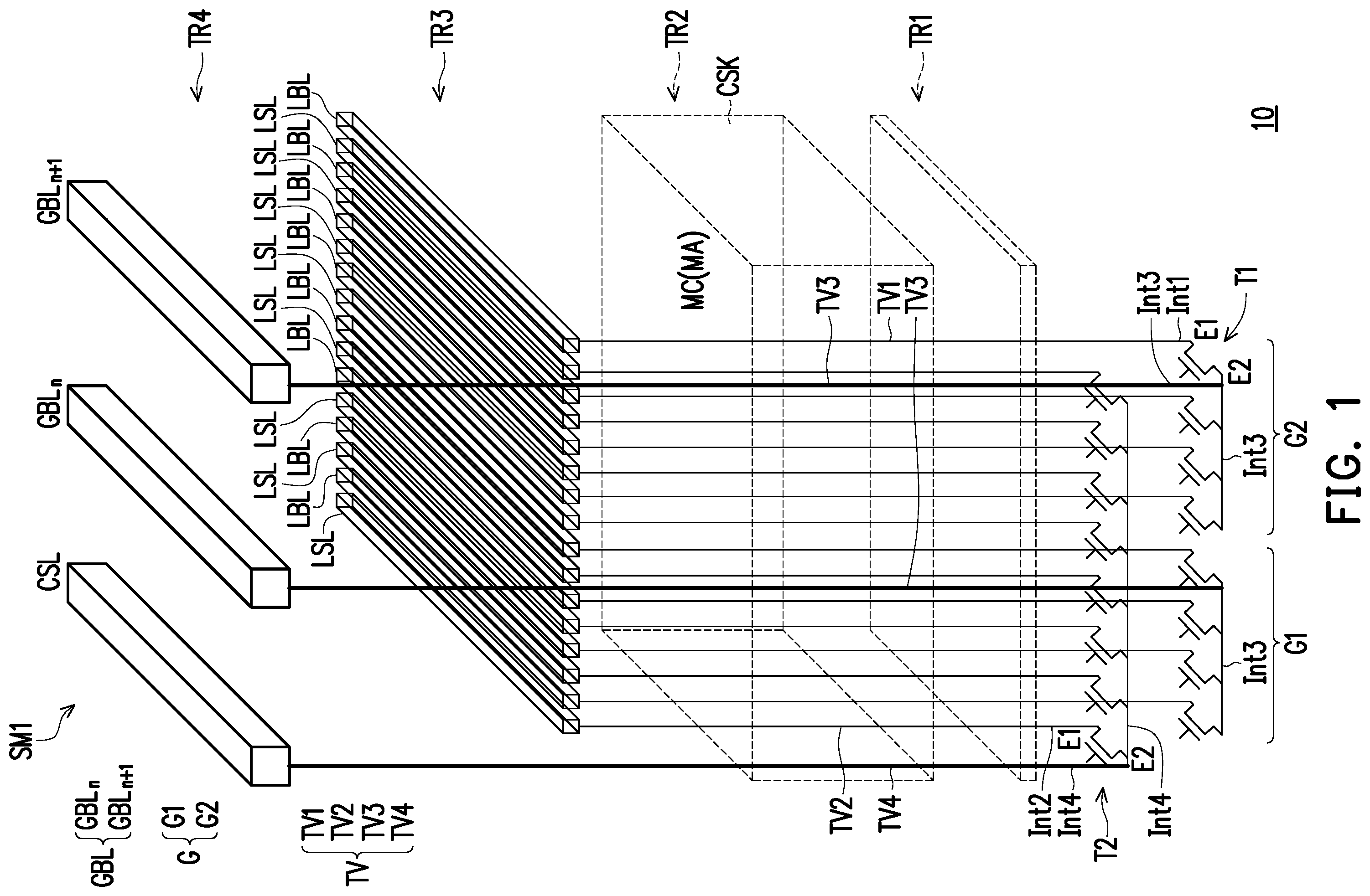
is a circuit diagram of a memory device according to an embodiment of the present disclosure. D is a top view of a memory device according to an embodiment of the present disclosure. D to D are schematic cross-sectional views taken along the lines III-III′ to VIII-VIII′ of A to D . Referring to , a memory device SM 1 according to an embodiment of the present disclosure includes a substrate 10 and first to fourth tiers TR 1 to TR 4 . Referring to , the first tier TR 1 is located on the substrate 10 . The first tier TR 1 includes multiple first transistors T 1 and multiple second transistors T 2 . In some embodiments, the number of first transistors T 1 is the same as the number of the second transistors T 2 . The multiple first transistors T 1 can be divided into multiple groups G, such as groups G 1 and G 2 . The multiple second transistors T 2 are not divided into groups. The second tier TR 2 is located on the first tier TR 1 . The second tier TR 2 includes a composite stacked structure CSK. The composite stacked structure CSK includes a memory array MA composed of multiple memory cells MC. The third tier TR 3 is located on the second tier TR 2 . The third tier TR 3 includes multiple local bit lines LBL and multiple local source lines LSL. The multiple local bit lines LBL and the multiple local source lines LSL are arranged alternately. The number of the local bit lines LBL is the same as the number of the local source lines LSL. The fourth tier TR 4 is located on the third tier TR 3 . The fourth tier TR 4 includes multiple global bit lines GBL and a common source line CSL. The global bit lines GBL may include global bit lines GBL n , GBL n+1 , etc. Each local bit line LBL and each local source line LSL are electrically connected to multiple memory cells MC in the composite stacked structure CSK (shown in D and D ). Each local bit line LBL is also electrically connected to the first terminal E 1 of one of the multiple first transistors T 1 . Each local source line LSL is connected to the first terminal E 1 of one of the multiple second transistors T 2 . Each global bit line GBL is electrically connected to multiple second terminals E 2 of the multiple first transistors T 1 in one of the multiple groups G. For example, the global bit line GBL n is connected to multiple second terminals E 2 of the multiple first transistors T 1 in the group G 1 . The global bit line GBL n+1 is connected to multiple second terminals E 2 of the multiple first transistors T 1 in the group G 2 . The common source line CSL is connected to the second terminal E 2 of each second transistor T 2 . In the embodiment of the present disclosure, multiple global bit lines GBL and only one common source line CSL are present at the fourth tier TR 4 . The number of common source line CSL is less than the number of global bit lines GBL. Therefore, the spacing between the common source line CSL and the global bit lines GBL at the fourth tier TR 4 is increased, and wider pitch and less wiring are provided for the back end of line (BEOL) process. Referring to D to D , the first tier TR 1 of the embodiment of the present disclosure may further include an interconnect structure 30 . The interconnect structure 30 includes a dielectric layer 22 and multiple interconnect lines Int 1 , Int 2 , Int 3 , Int 4 . The dielectric layer 22 covers the substrate 10 and the multiple first transistors T 1 and the multiple second transistors T 2 . Multiple interconnect lines Int 1 , multiple interconnect lines Int 2 , multiple interconnect lines Int 3 , and single interconnect line Int 4 may include wires and plugs, respectively. Referring to and D , each interconnect line Int 1 is connected to the first terminal E 1 of the first transistor T 1 . Each interconnect line Int 3 is connected to the second terminal E 2 of the first transistor T 1 , and is connected to multiple second terminals E 2 of the multiple first transistors T 1 that are in the same group G. Referring to and D , each interconnect line Int 2 is connected to the first terminal E 1 of the second transistor T 2 . The interconnect line Int 4 is connected to the second terminal E 2 of the second transistor T 2 , and is connected to multiple second terminals E 2 of the multiple first transistors T 2 that are not grouped. Referring to and D , the composite stacked structure CSK at the second tier TR 2 includes a first stacked structure SK 1 (shown in D to D ) and a second stacked structure SK 2 (shown in D and D ). Referring to D to D , the first stacked structure SK 1 of the composite stacked structure CSK is located in a periphery region R 2 . The first stacked structure SK 1 includes multiple insulating layers 102 and multiple intermediate layers 104 stacked alternately. Referring to D to D , the second tier TR 2 further includes multiple through vias TV. The multiple through vias TV extend through the composite stacked structure CSK. The multiple through vias TV include multiple through vias TV 1 , multiple through vias TV 2 , multiple through vias TV 3 and single through via TV 4 . Referring to and D , a first through via TV 1 extends through the first stacked structure SK 1 , and is electrically connected to the first terminal E 1 of the first transistor T 1 through an interconnect line Int 1 . Referring to D , a second through via TV 2 extends through the first stacked structure SK 1 , and is electrically connected to the first terminal E 1 of the second transistor T 2 through an interconnect line Int 2 . The number of first through vias TV 1 is equal to the number of second through vias TV 2 , as shown in B . Referring to and D , one of the third through vias TV 3 extends through the first stacked structure SK 1 , and is electrically connected to the multiple second terminals E 2 of the multiple first transistors T 1 in the group G 1 through the interconnect line Int 3 . Referring to , another one of the third through vias TV 3 extends through the first stacked structure SK 1 , and is electrically connected to the second terminals E 2 of the first transistors T 1 in the group G 2 through another interconnect line Int 3 . Referring to and D , the fourth through via TV 4 extends through the first stacked structure SK 1 , and is electrically connected to the second terminal E 2 of each second transistor T 2 through an interconnect line Int 4 . Therefore, the number of fourth through via TV 4 is less than the number of multiple third through vias TV 3 , as shown in C . Referring to D and D , the second stacked structure SK 2 of the composite stacked structure CSK is located in a memory plane region R 1 . The second stacked structure SK 2 includes multiple insulating layers 102 and multiple conductive layers 126 stacked alternately. The second tier TR 2 also includes multiple channel pillars CP and multiple charge storage structures 108 . The multiple channel pillars CP extend through the second stacked structure SK 2 . The multiple charge storage structures 108 are interposed between the multiple channel pillars CP and the second stacked structure SK 2 . The multiple conductive layers 126 , the multiple channel pillars CP and the multiple charge storage structures 108 form multiple memory cells MC. Multiple memory cells MC form a memory array MA. Referring to D and D , each local bit line LBL located at the third tier TR 3 is electrically connected to one of the multiple channel pillars CP (shown in ) through a contact COA 5 , and is electrically connected to the first terminal E 1 (shown in D ) of one of the multiple first transistors T 1 through a contact COA 1 , a first through via TV 1 and an interconnect line Int 1 . Referring to D and D , each local source line LSL located at the third tier TR 3 is electrically connected to another one of the multiple channel pillars CP (shown in D ) through a contact COA 6 , and is electrically connected to the first terminal E 1 (shown in D ) of one of the multiple second transistors T 2 through a contact COA 2 , a second through via TV 2 and an interconnect line Int 2 . Referring to D , each of multiple global bit lines GBL located at the fourth tier TR 4 is electrically connected to multiple second terminals E 2 of the multiple first transistors T 1 in the same group G through a contact COA 3 ′, a connection pad LP 3 , a contact COA 3 , a third through via TV 3 and an interconnect line Int 3 , as shown in . Referring to D , the common source line CSL at the fourth tier TR 4 is electrically connected to the second terminal E 2 of each second transistor T 2 through a contact COA 4 ′, a connection pad LP 4 , a contact COA 4 , a fourth through via TV 4 , and an interconnect line Int 4 , as shown in . Referring to D and D , D , and D , the local bit line LBL and the global bit line GBL can be electrically connected to the first transistor T 1 through the through vias TV 1 and TV 3 respectively. The local source line LSL and the common source line CSL can be electrically connected to the second crystal T 2 through the through vias TV 2 and TV 4 respectively. Each local bit line LBL is electrically connected to the first terminal E 1 of one of the first transistors T 1 through one of the first through vias TV 1 . Each local source line LSL is electrically connected to the first terminal E 1 of one of the multiple second transistors T 2 through the second through via TV 2 . The number of first through vias TV 1 is equal to the number of second through vias TV 2 . Each global bit line GBL is electrically connected to multiple second terminals E 2 of the multiple first transistors T 1 in one of the multiple groups G through one of the multiple third vias TV 3 . The common source line CSL is electrically connected to the second terminal E 2 of each second transistor T 2 through the fourth through via TV 4 . Therefore, the number of fourth through via TV 4 is less than the number of multiple third through vias TV 3 . A to D are top views of a method of fabricating a memory device according to an embodiment of the present disclosure. A to D are schematic cross-sectional views taken along the line III-III′ of A to D . A to D are schematic cross-sectional views taken along the line IV-IV′ of A to D . A to D are schematic cross-sectional views taken along the line V-V′ of A to D . A to D are schematic cross-sectional views taken along the line VI-VI′ of A to D . A to D are schematic cross-sectional views taken along the line VII-VII′ of A to D . A to D are schematic cross-sectional views of the line VIII-VIII′ of A to D . Referring to A to A , a substrate 10 is provided. The substrate 10 can be a semiconductor substrate or a semiconductor compound substrate, such as a silicon-containing substrate or a silicon-germanium substrate. The substrate 10 includes a memory plane region R 1 and a periphery region R 2 . A first tier TR 1 is formed on the substrate 10 . First, multiple transistors are formed on a substrate 10 . The multiple transistors include first transistors T 1 and second transistors T 2 in the periphery region R 2 . The first transistors T 1 and the second transistors T 2 can be N-type metal oxide semiconductor (NMOS) transistors, P-type metal oxide semiconductor (PMOS) transistors or complementary metal oxide semiconductor (CMOS) devices. Referring to A and A , next, an interconnect structure 30 is formed on the first transistors T 1 and the second transistors T 2 . The interconnect structure 30 includes multiple dielectric layers 22 and interconnect lines Int 1 , Int 2 , Int 3 , Int 4 formed in the multiple dielectric layers 22 . The interconnect lines Int 1 , Int 2 , Int 3 , Int 4 include multiple plugs (not shown) and multiple wires (not shown) and the like. The interconnect line Int 1 is connected to the first terminals E 1 of multiple first transistors T 1 . The interconnect line Int 2 is connected to the first terminals E 1 of multiple second transistors T 2 . The interconnect line Int 3 is connected to the second terminals E 2 of multiple first transistors T 1 . The interconnect line Int 4 is connected to the second terminals E 2 of the multiple second transistors T 2 . The interconnect lines Int 1 , Int 2 , Int 3 , Int 4 can be formed by single damascene, dual damascene process or any known method. The interconnect line may include a barrier material and a metal material. In one embodiment, the barrier material includes titanium (Ti), titanium nitride (TiN), tantalum (Ta), tantalum nitride (TaN) or a combination thereof. The metal material includes tungsten (W). Referring to B to B , a first stacked structure SK 1 is formed on the first tier TR 1 . The first stacked structure SK 1 is formed on the interconnect structure 30 in the memory plane region R 1 and the periphery region R 2 . The first stacked structure SK 1 includes multiple insulating layers 102 and multiple intermediate layers 104 stacked alternately. In some embodiments, the material of the insulating layers 102 includes silicon oxide, and the material of the intermediate layers 104 includes silicon nitride. The intermediate layers 104 can serve as sacrificial layers, which will be partially removed in subsequent processes. In some embodiments, the first stacked structure SK 1 further includes a conductive layer 103 . The conductive layer 103 is located on the lowermost insulating layer 102 . The conductive layer 103 can serve as an etch stop layer. The conductive layer 103 may include polysilicon. Referring to B and B , a vertical channel pillar CP is formed in the first stacked structure SK 1 of the memory plane region R 1 (as shown in B ), and an insulating pillar IP is formed in the first stacked structure SK 1 of the periphery region R 2 (as shown in B ), and B and B and B ). Referring to B and B , a vertical channel pillar CP is formed in the first stacked structure SK 1 in the memory plane region R 1 includes the following steps. First, an opening 106 is formed in the first stacked structure SK 1 . In one embodiment, the opening 106 may have substantially vertical sidewalls. In another embodiment, opening 106 may have slightly inclined sidewalls (not shown). In one embodiment, the opening 106 is also called a vertical channel (VC) hole. In one embodiment, the opening 106 can be formed by single-stage lithography and etching processes. In another embodiment, the opening 106 is formed by multi-stage e lithography and etching processes. The profile of the sidewall of the opening 106 formed by multi-stage lithography and etching processes may be bamboo-shaped. A charge storage structure 108 is then formed in the opening 106 . The charge storage structure 108 is in contact with the insulating layers 102 and the intermediate layers 104 . In one embodiment, the charge storage structure 108 is an oxide/nitride/oxide (ONO) composite layer. The charge storage structure 108 may be a conformal layer formed on the sidewall and the bottom surface of the opening 106 . Thereafter, a vertical channel pillar CP is formed in the remaining space of the opening 106 . The vertical channel pillar CP can be formed by the following steps. A channel layer 110 is formed on the inner sidewall and the bottom surface of the charge storage structure 108 . In one embodiment, the material of the channel layer 110 includes undoped polysilicon. Next, an insulating pillar (or called a core insulating pillar) 112 is formed on the inner surface of the channel layer 110 . In one embodiment, the material of the insulating pillar 112 includes silicon oxide. Afterwards, a channel plug 114 is formed in the opening 106 , and the channel plug 114 is in contact with the channel layer 110 . The channel plug 114 extends from the top surface (not shown) of the uppermost insulating layer 102 to a certain depth of the opening 106 . In one embodiment, the material of the channel plug 114 includes doped semiconductor material, such as doped polysilicon. The channel layer 110 , the insulating pillar 112 and the channel plug 114 may be collectively referred to as a vertical channel pillar CP. The vertical channel pillar CP penetrates through the stacked structure SK 1 and extends to the conductive layer 103 . The charge storage structure 108 surrounds the vertical outer surface of the vertical channel pillar CP. Referring to B to B , an insulating pillar IP is formed in the first stacked structure SK 1 in the periphery region R 2 includes the following steps. First, an opening 106 ′ is formed in the first stacked structure SK 1 in the periphery region R 2 . In one embodiment, the opening 106 ′ may have substantially vertical sidewalls. In another embodiment, the opening 106 ′ may have slightly inclined sidewalls (not shown). The opening 106 ′ may be formed simultaneously with, formed before, or formed after the opening 106 . The opening 106 ′ can be formed by single-stage lithography and etching processes. In another embodiment, the opening 106 ′ is formed by multi-stage lithography and etching processes. The profile of the sidewall of the opening 106 ′ formed by multi-stage lithography and etching processes may be bamboo-shaped. Afterwards, an insulating material is formed on the first stacked structure SK 1 and in the opening 106 ′, and then, a chemical mechanical polishing process or an etch-back process is performed to remove excess insulating material to form an insulating pillar IP. Referring to C and C to C , a dielectric layer 115 is formed on the substrate 10 in the memory plane region R 1 and the periphery region R 2 . The material of the dielectric layer 115 includes silicon oxide. Next, the multiple intermediate layers 104 of the first stacked structure SK 1 in the memory plane region R 1 are replaced with multiple conductive layers 126 (shown in C and C ), and the intermediate layers 104 of the first stacked structure SK 1 in the periphery region R 2 remain (shown in C and C and C and C ). Referring to B and C , the method of replacing the multiple intermediate layers 104 of the first stacked structure SK 1 in the memory plane region R 1 with multiple conductive layers 126 includes the following steps. First, a patterning process is performed on the first stacked structure SK 1 in the memory plane region R 1 to form one or more separation trenches. The separation trench extends through the dielectric layer 115 and the first stacked structure SK 1 , so that the intermediate layers 104 and the insulating layers 102 are exposed. The separation trench may have vertical sidewalls (not shown) or slightly sloped sidewalls (not shown). Next, a selective etching process is performed to make the etchant contact the intermediate layers 104 of the first stacked structure SK 1 at both sides through the separation trench. Thereby, portions the intermediate layers 104 are removed to form multiple horizontal openings (not shown), portions of the intermediate layers 104 remain in the periphery region R 2 , as shown in C and C and C . The selective etching process can be an isotropic etching process, such as a wet etching process. The etchant used in the wet etching process may include hot phosphoric acid. Then, a conductive layer 126 is formed in the separation trench and each horizontal opening, as shown in C . The conductive layers 126 can serve as gate layers. The conductive layer 126 may include a barrier layer and a metal layer. In one embodiment, the material of the barrier layer includes titanium (Ti), titanium nitride (TiN), tantalum (Ta), tantalum nitride (TaN) or a combination thereof. The material of the metal layer includes tungsten (W). Portions of the intermediate layers 104 in the memory plane region R 1 are replaced by conductive layers 126 , and portions of the intermediate layers 104 remain in the periphery region R 2 (shown in C and C and C and C ). The multiple insulating layers 102 and the multiple conductive layers 126 form a second stacked structure SK 2 . The second stacked structure SK 2 in the memory plane region R 1 and the first stacked structure SK 1 remaining in the periphery region R 2 together form a composite stacked structure CSK. Referring to C and C to C and C , through vias TV 1 , TV 2 , TV 3 and TV 4 are formed in the dielectric layer 115 and the insulating pillar IP in the periphery region R 2 . The through vias TV 1 and TV 2 are respectively connected to interconnect lines Int 1 and Int 2 . The through vias TV 3 and TV 4 are respectively connected to interconnect lines Int 3 and Int 4 . The method of forming the through vias TV 1 , TV 2 , TV 3 , TV 4 is described in the following steps, for example. First, lithography and etching processes are performed to form openings (not shown) in the insulating pillars IP. A conductive material is then formed over the dielectric layer 115 and in the openings. Afterwards, a chemical mechanical polishing process or an etch-back process is performed to remove excess conductive material on the dielectric layer 115 . The conductive material includes a barrier material and a metal material. In one embodiment, the barrier material includes titanium (Ti), titanium nitride (TiN), tantalum (Ta), tantalum nitride (TaN) or a combination thereof. The metal material includes tungsten (W). So far, the dielectric layer 115 , the composite stacked structure CSK and the through vias TV 1 , TV 2 , TV 3 , TV 4 form a second tier TR 2 . Referring to D to D , a third tier TR 3 is formed on the second tier TR 2 . The third tier TR 3 may include dielectric layers 128 , 130 , contacts COA 1 to COA 6 , local bit lines LBL, local source lines LSL, and connection pads LP 3 and LP 4 . A dielectric layer 128 is formed on the dielectric layer 115 . A dielectric layer 130 is formed on dielectric layer 128 . The dielectric layers 128 , 130 may include silicon oxide. The contacts COA 1 to COA 4 are formed in the dielectric layer 128 and are electrically connected to the through vias TV 1 to TV 4 respectively. The contacts COA 5 and COA 6 are formed in the dielectric layers 128 and 115 and are electrically connected to the channel pillar CP. The local bit line LBL is formed in the dielectric layer 130 and is electrically connected to the contact COA 1 . The local source line LSL is formed in the dielectric layer 130 and electrically connected to the contact COA 2 . The connection pad LP 3 is formed in the dielectric layer 130 and is electrically connected to the contact COA 3 . The connection pad LP 4 is formed in the dielectric layer 130 and is electrically connected to the contact COA 4 . The connection pads LP 3 and LP 4 can be formed simultaneously when forming the local bit line LBL and the local source line LSL. The contacts COA 1 to COA 6 , the local bit lines LBL, the local source lines LSL, the connection pads LP 3 and LP 4 can be formed by single damascene or dual damascene processes, or any known method, and will not be described in detail herein. Referring to D and D to D , a fourth tier TR 4 is formed on the third tier TR 3 . The fourth tier TR 4 may include a dielectric layer 132 , contacts COA 3 ′ and COA 4 ′, a global bit line GBL, a common source line CSL and a protection layer 134 . The dielectric layer 132 is formed on the dielectric layer 130 . The dielectric layer 132 may include silicon oxide. The contacts COA 3 ′, COA 4 ′ are formed in the dielectric layer 132 and are electrically connected to the connection pads LP 3 , LP 4 respectively. The global bit line GBL and the common source line CSL are formed on the dielectric layer 132 and electrically connected to the contacts COA 3 ′ and COA 4 ′ respectively. The contacts COA 3 ′, COA 4 ′, the global bit line GBL, and the common source line CSL can be formed by, for example, single damascene or dual damascene process, or any known method, and will not be described in detail herein. The protection layer 134 may include silicon oxide, silicon nitride or a combination thereof. So far, the fabrication of the memory device SM 1 is completed. The transistors in the above embodiments may be complementary metal-oxide-semiconductor (CMOS) devices. Since the transistors are formed under the memory array, this architecture can also be called a complementary metal-oxide-semiconductor device under the memory array (CMOS-Under-Array, CUA) structure. However, the present disclosure is not limited thereto. In other embodiments, the complementary metal-oxide-semiconductor device (CMOS) can also be bonded together with the memory array, so this architecture can also be called a bonded complementary metal-oxide-semiconductor device bonded memory array (CMOS-Bonded-Array, CbA) structure. The embodiments of the present disclosure may be applied to a 3D NOR flash memory and a 3D AND flash memory. To sum up, the embodiment of the present disclosure uses a common source line to save space. Therefore, the spacing between the common source line (CSL) and the global bit lines (GBL) at the same tier can be increased. Due to the common source line design, the wider pitch and less wiring are provided for the back end of line (BEOL) process, so as to reduce the CSL/GBL short rate.
Figures (20)
Citations
This patent cites (3)
- US2022/0020761
- US4174864
- US202316423