Abstract
A piezoelectric actuator includes a piezoelectric element having a rectangular shape, a first supporter, and a second supporter. The piezoelectric element includes a pair of main surfaces opposing each other, a first end surface and a second end surface opposing each other in a long side direction of the pair of main surfaces, and a first side surface and a second side surface opposing each other in a short side direction of the pair of main surfaces. The first supporter is provided to be movable according to deformation of the first end surface. The second supporter is provided to be movable according to deformation of the first side surface. The first supporter includes an opposing portion and a protruding portion. The opposing portion opposes the second supporter in the long side direction. The protruding portion protrudes from the opposing portion and abuts on the second supporter.
Claims (9)
1 . A piezoelectric actuator for driving an object, comprising: a piezoelectric element having a rectangular shape and including a pair of main surfaces opposing each other, a first end surface and a second end surface opposing each other in a long side direction of the pair of main surfaces, and a first side surface and a second side surface opposing each other in a short side direction of the pair of main surfaces; a first supporter opposing the object in the long side direction via the piezoelectric element and supporting the first end surface; and a second supporter opposing a disposition surface of a housing in which the piezoelectric element is disposed in the short side direction via the piezoelectric element and supporting the first side surface, wherein the first supporter is provided to be movable according to deformation of the first end surface, the second supporter is provided to be movable according to deformation of the first side surface, and the first supporter includes an opposing portion opposing the second supporter in the long side direction, and a protruding portion protruding from the opposing portion in the long side direction and abutting on the second supporter.
Show 8 dependent claims
2 . The piezoelectric actuator according to claim 1 , wherein a distance at which an abutting portion of the protruding portion with the second supporter is spaced apart from the piezoelectric element in the short side direction is 0.3 times or more and 0.7 times or less of a length of the piezoelectric element in the short side direction.
3 . The piezoelectric actuator according to claim 1 , further comprising: a first biasing member biasing the first supporter in the long side direction to bring the first supporter into contact with the piezoelectric element; and a second biasing member biasing the second supporter in the short side direction to bring the second supporter into contact with the piezoelectric element.
4 . The piezoelectric actuator according to claim 1 , further comprising: a first biasing member biasing the first supporter in the long side direction to bring the first supporter into contact with the piezoelectric element; and a second biasing member biasing the second supporter in the short side direction to bring the second supporter into contact with the piezoelectric element, wherein the second supporter includes a pair of support portions spaced apart from each other in the long side direction and supporting the first side surface, and the second biasing member is located between the pair of support portions in the long side direction.
5 . The piezoelectric actuator according to claim 1 , wherein the second supporter includes a pair of support portions spaced apart from each other in the long side direction and supporting the first side surface.
6 . The piezoelectric actuator according to claim 4 , wherein each of the pair of support portions includes a curved surface that abuts on the piezoelectric element.
7 . The piezoelectric actuator according to claim 1 , wherein the protruding portion includes a curved surface.
8 . The piezoelectric actuator according to claim 1 , wherein the first supporter includes a positioning portion that defines a position of the piezoelectric element in the short side direction.
9 . The piezoelectric actuator according to claim 1 , wherein the first supporter is rotatably connected to the second supporter by a coupling shaft provided on the protruding portion.
Full Description
Show full text →
TECHNICAL FIELD
The present disclosure relates to piezoelectric actuators. This application is based upon and claims the benefit of priority from Japanese Patent Application No. 2022-009907, filed on Jan. 26, 2022, the entire contents of which are incorporated herein by reference.
BACKGROUND
WO2010/013361 discloses a holding device for a piezoelectric vibrator used as a piezoelectric actuator. In this holding device, since the piezoelectric vibrator is held by the plate spring fixed to the side portion of the piezoelectric vibrator, the loss of vibration energy of the piezoelectric vibrator is small.
SUMMARY
In the above-described holding device, it is necessary to fix the plate spring to the piezoelectric vibrator and a support member. For this reason, it takes time to assemble. An aspect of the present disclosure provides a piezoelectric actuator that is easy to assemble without reducing vibration efficiency of a piezoelectric element. A piezoelectric actuator according to an aspect of the present disclosure is for driving an object. The piezoelectric actuator includes a piezoelectric element having a rectangular shape, a first supporter, and a second supporter. The piezoelectric element includes a pair of main surfaces opposing each other, a first end surface and a second end surface opposing each other in a long side direction of the pair of main surfaces, and a first side surface and a second side surface opposing each other in a short side direction of the pair of main surfaces. The first supporter is provided to be movable according to deformation of the first end surface. The second supporter is provided to be movable according to deformation of the first side surface. The first supporter includes an opposing portion and a protruding portion. The opposing portion opposes the second supporter in the long side direction. The protruding portion protrudes from the opposing portion in the long side direction and abuts on the second supporter. In the piezoelectric actuator, the first supporter is provided to be movable according to the deformation of the first end surface of the piezoelectric element. The second supporter is provided to be movable according to the deformation of the first side surface of the piezoelectric element. Since the first supporter and the second supporter are provided to be separately movable as described above, the vibration of the piezoelectric element is less likely to be inhibited. The first supporter includes a protruding portion that abuts on the second supporter. Therefore, the position of the second supporter relative to the first supporter is easily determined at the time of assembly. Therefore, assembly is easy. A distance at which an abutting portion of the protruding portion with the second supporter is spaced apart from the piezoelectric element in the short side direction may be 0.3 times or more and 0.7 times or less of a length of the piezoelectric element in the short side direction. In this case, even if the first supporter and the second supporter move according to the vibration of the piezoelectric element, the first supporter and the second supporter are prevented from interfering with each other. Therefore, the vibration of the piezoelectric element is less likely to be disturbed. The piezoelectric actuator may further include a first biasing member and a second biasing member. The first biasing member biases the first supporter in the long side direction to bring the first supporter into contact with the piezoelectric element. The second biasing member biases the second supporter in the short side direction to bring the second supporter into contact with the piezoelectric element. In this case, a configuration in which the first supporter is movable according to the deformation of the first end surface is easily realized. A configuration in which the second supporter is movable according to the deformation of the first side surface is easily realized. The piezoelectric actuator may further include a first biasing member and a second biasing member. The first biasing member biases the first supporter in the long side direction to bring the first supporter into contact with the piezoelectric element. The second biasing member biases the second supporter in the short side direction to bring the second supporter into contact with the piezoelectric element. The second supporter may include a pair of support portions spaced apart from each other in the long side direction and supporting the first side surface. The second biasing member may be located between the pair of support portions in the long side direction. In this case, a configuration in which the first supporter is movable according to the deformation of the first end surface is easily realized. A configuration in which the second supporter is movable according to the deformation of the first side surface is easily realized. Since the second supporter supports the first side surface by the pair of support portions, it can reliably support the first side surface. Since the second biasing member is located between the pair of support portions in the long side direction, the biasing force can be applied to the pair of support portions in a balanced manner. The second supporter may include a pair of support portions. The pair of support portions are spaced apart from each other in the long side direction. The pair of support portions support the first side surface. In this case, since the second supporter supports the first side surface by a pair of support portions, the first side surface can be reliably supported. Each of the pair of support portions may include a curved surface that abuts on the piezoelectric element. In this case, damage to the pair of support portions and damage to the piezoelectric element due to contact between the pair of support portions and the piezoelectric element are suppressed. The protruding portion may include a curved surface. In this case, damage to the protruding portion and damage to the second supporter due to contact between the protruding portion and the second supporter are suppressed. The first supporter includes a positioning portion that defines a position of the piezoelectric element in the short side direction. In this case, it is possible to prevent the piezoelectric element from moving in the short side direction on the first supporter. The first supporter may be rotatably connected to the second supporter by a coupling shaft provided on the protruding portion. In this case, since the position of the second supporter is reliably determined with respect to the first supporter, the assembly is easier.
BRIEF DESCRIPTION OF THE DRAWINGS
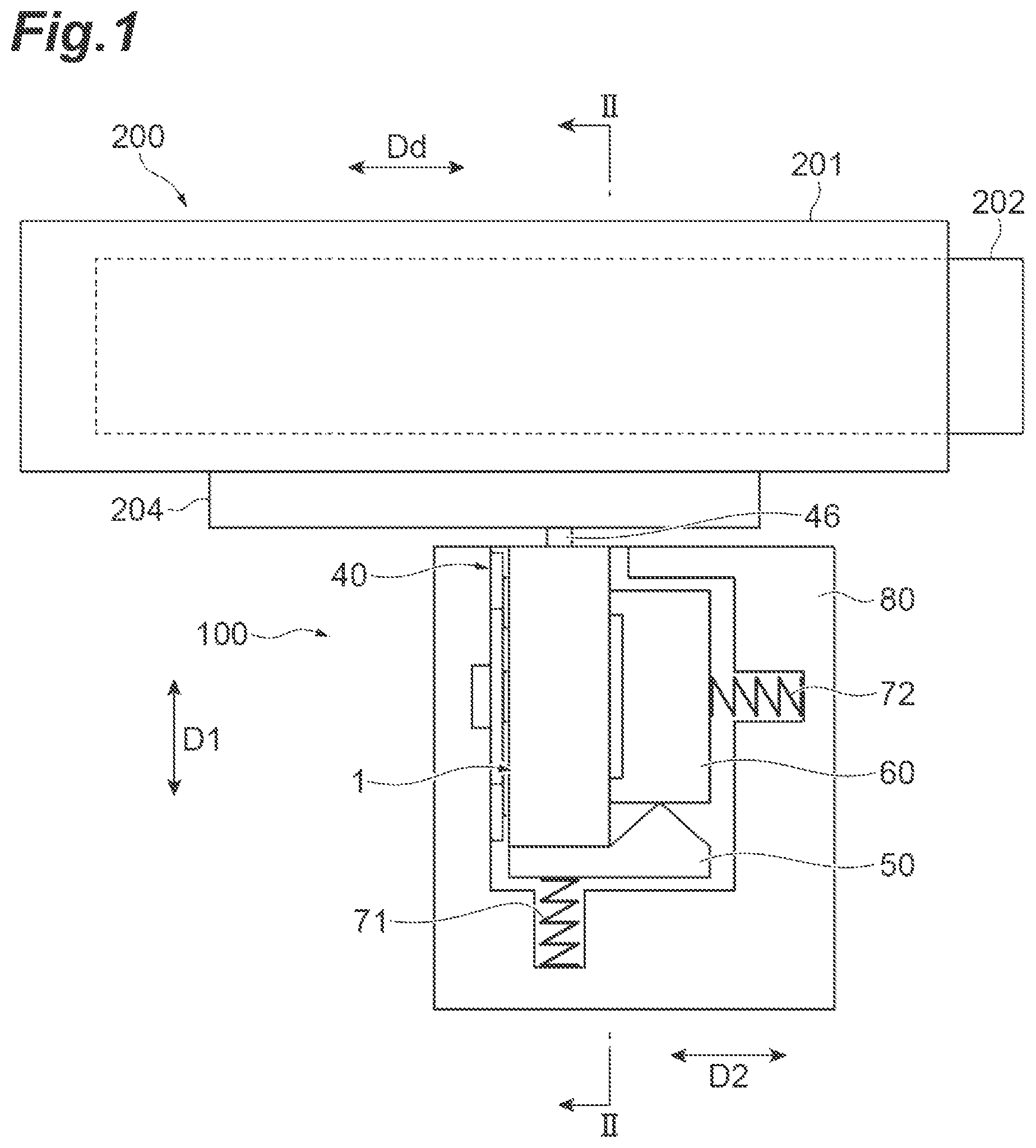
is a side view illustrating a piezoelectric actuator according to a first embodiment and a moving object. is a cross-sectional view taken along line II-II of . is a cross-sectional view taken along line III-III of . is a perspective view of the piezoelectric element of . is a cross-sectional view taken along line V-V of . is a cross-sectional view taken along line VI-VI of . is an exploded perspective view of the piezoelectric element of . is a plan view illustrating an internal electrode disposed on a piezoelectric layer. is a plan view illustrating internal electrodes disposed on a piezoelectric layer. is a plan view illustrating internal electrodes disposed on a piezoelectric layer. is a side view illustrating a piezoelectric element, a contact, a first supporter, and a second supporter. A, 12 B, and 12 C are side views schematically illustrating movements of the piezoelectric actuator of . A, 13 B, and 13 C are side views schematically illustrating movements of a piezoelectric actuator according to a comparative example. of a piezoelectric actuator according to a comparative example. is a graph showing the relationship between the frequency of the voltage applied to the piezoelectric element and the moving speed of the moving object. is a side view illustrating a piezoelectric actuator according to a second embodiment. is a side view illustrating a piezoelectric actuator according to a third embodiment. is a cross-sectional view taken along line XVII-XVII of .
DETAILED DESCRIPTION
Hereinafter, embodiments will be described in detail with reference to the accompanying drawings. In the description of the drawings, the same or corresponding elements are denoted by the same reference numerals, and redundant description is omitted. First Embodiment As illustrated in to 3 , a piezoelectric actuator 100 according to a first embodiment includes a piezoelectric element 1 , a wiring member 40 , a contact 46 , a first supporter 50 , a second supporter 60 , a first biasing member 71 , a second biasing member 72 , and a housing 80 . The piezoelectric actuator 100 is used as an ultrasonic motor and is configured to be capable of driving a moving object 200 , which is a driven object, in a driving direction Dd. In , the moving object 200 is not shown. (Moving Object) The moving object 200 includes a rail 201 , a shaft member 202 , a plurality of pairs of a bearing 203 , and a sliding plate 204 . The rail 201 is a groove-like member having a U-shaped cross section and extending in the driving direction Dd. The rail 201 includes a bottom 201 a and a pair of a side portion 201 b opposed to each other. A groove extending in the driving direction Dd is provided on an inner surface of each side 201 b . The shaft member 202 is a rod-shaped member having a rectangular cross section and extends in the driving direction Dd. The shaft member 202 is fitted into the groove of the rail 201 . On the outer side surface of the shaft member 202 , a groove extending in the driving direction Dd is provided at a position opposing the groove provided on the inner surface of each side 201 b. The bearing 203 is disposed between the groove of the side portion 201 b of the rail 201 and the groove of the shaft member 202 . The sliding plate 204 is attached to one side portion 201 b of the rail 201 and extends in the driving direction Dd. In the moving object 200 , the vibration of the piezoelectric actuator 100 is transmitted to the rail 201 via the sliding plate 204 , and the rail 201 is driven in the driving direction Dd together with the sliding plate 204 . (Piezoelectric Element) The piezoelectric element 1 will be described with reference to to 10 . As shown in , the piezoelectric element 1 includes a piezoelectric element body 2 and a plurality of external electrodes 4 , 5 , 6 , 7 , 8 , and 9 . The piezoelectric element body 2 has a rectangular parallelepiped shape. The rectangular parallelepiped shape includes a rectangular parallelepiped shape in which corners and ridge portions are chamfered, and a rectangular parallelepiped shape in which corners and ridge portions are rounded. The piezoelectric element body 2 includes a pair of end surfaces 2 a and 2 b opposing each other, a pair of side surfaces 2 c and 2 d opposing each other, and a pair of main surfaces 2 e and 2 f opposing each other. An opposing direction D 1 of the end surfaces 2 a and 2 b , an opposing a direction D 2 of the side surfaces 2 c and 2 d , and an opposing a direction D 3 of the main surfaces 2 e and 2 f intersect each other. In the present embodiment, the direction D 1 , the direction D 2 , and the direction D 3 are orthogonal to each other. The direction D 1 is a length direction of the piezoelectric element body 2 . The direction D 2 is a width direction of the piezoelectric element body 2 . The direction D 3 is a thickness direction of the piezoelectric element body 2 . Each of the main surfaces 2 e and 2 f has a rectangular shape. A long side direction of the main surfaces 2 e and 2 f coincides with the direction D 1 . A short side direction of the main surfaces 2 e and 2 f coincides with the direction D 2 . Each end surfaces 2 a and 2 b extends in the direction D 2 so as to connect the side surfaces 2 c and 2 d . Each end surfaces 2 a and 2 b also extends in the direction D 3 so as to connect the main surfaces 2 e and 2 f . Each side surfaces 2 c and 2 d extends in the direction D 1 so as to connect the end surfaces 2 a and 2 b . Each side surfaces 2 c and 2 d also extends in the direction D 3 so as to connect the main surfaces 2 e and 2 f . Each main surfaces 2 e and 2 f extends in the direction D 1 so as to connect the end surfaces 2 a and 2 b . Each main surfaces 2 e and 2 f also extends in the direction D 2 so as to connect the side surfaces 2 c and 2 d. The width (the length in the direction D 2 ) of the piezoelectric element body 2 is, for example, 2.5 mm. The length (the length in the direction D 1 ) of the piezoelectric element body 2 is, for example, 9 mm. The thickness (the length in the direction D 3 ) of the piezoelectric element body 2 is, for example, 1 mm. The width of the piezoelectric element body 2 is longer than the thickness of the piezoelectric element body 2 and shorter than the length of the piezoelectric element body 2 . Each surfaces 2 a , 2 b , 2 c , 2 d , 2 e , and 2 f of the piezoelectric element body 2 is polished surfaces polished by barrel polishing, for example. Each ridge portion 2 g positioned between two adjacent surfaces among the surfaces 2 a , 2 b , 2 c , 2 d , 2 e , and 2 f has a rounded chamfered shape. Each ridge portion 2 g has is constituted by a curved surface. Each corner portion 2 h positioned among three adjacent surfaces among the surfaces 2 a , 2 b , 2 c , 2 d , 2 e , and 2 f has a rounded chamfered shape. Each corner portion 2 h is constituted by a curved surface. The external electrodes 4 , 5 , and 6 are arranged in the side surface 2 c of the piezoelectric element body 2 . The external electrodes 4 , 5 , and 6 are separated from each other. The external electrodes 4 , 5 , and 6 are arranged side by side in the direction D 1 . The external electrode 4 is disposed on the end surface 2 a side. The external electrode 4 is spaced apart from the end surface 2 a . The external electrode 5 is disposed on the end surface 2 b side. The external electrode 5 is spaced apart from the end surface 2 b . The external electrode 6 is disposed between the external electrode 4 and the external electrode 5 . The external electrode 6 is spaced apart from each of the external electrode 4 and the external electrode 5 . The external electrodes 4 , 5 , and 6 have the same shape. Each of the external electrodes 4 , 5 , and 6 has a rectangular shape when viewed from the direction D 2 . Each of the external electrodes 4 , 5 , and 6 extends in the direction D 3 so as to connect the main surface 2 e and the main surface 2 f . Each of the external electrodes 4 , 5 , and 6 is formed on the entire side surface 2 c in the direction D 3 . The external electrodes 4 , 5 , and 6 are also provided on each of the ridge portion 2 g between the side surface 2 c and the main surface 2 e and the ridge portion 2 g between the side surface 2 c and the main surface 2 f. The external electrodes 7 , 8 , and 9 are arranged in the side surface 2 d of the piezoelectric element body 2 . The external electrodes 7 , 8 , and 9 are separated from each other. The external electrodes 7 , 8 , and 9 are arranged side by side in the direction D 1 . The external electrode 7 is disposed on the end surface 2 a side. The external electrode 7 is spaced apart from the end surface 2 a . The external electrode 8 is disposed on the end surface 2 b side. The external electrode 8 is spaced apart from the end surface 2 b . The external electrode 9 is disposed between the external electrode 7 and the external electrode 8 . The external electrode 9 is spaced apart from each of the external electrode 7 and the external electrode 8 . The external electrodes 7 , 8 , and 9 have the same shape. Each of the external electrodes 7 , 8 , and 9 has a rectangular shape when viewed from the direction D 2 . Each of the external electrodes 7 , 8 , and 9 extends in the direction D 3 so as to connect the main surface 2 e and the main surface 2 f . Each of the external electrodes 7 , 8 , and 9 is formed on the entire side surface 2 d in the direction D 3 . The external electrodes 7 , 8 , and 9 are also provided on each of the ridge portion 2 g between the side surface 2 d and the main surface 2 e and the ridge portion 2 g between the side surface 2 d and the main surface 2 f. The external electrode 4 and the external electrode 7 oppose each other in the direction D 2 . The external electrode 4 and the external electrode 7 are provided so as to overlap each other when viewed from the direction D 2 . The external electrode 5 and the external electrode 8 oppose each other in the direction D 2 . The external electrode 5 and the external electrode 8 are provided so as to overlap each other when viewed from the direction D 2 . The external electrode 6 and the external electrode 9 oppose each other in the direction D 2 . The external electrode 6 and the external electrode 9 are provided so as to overlap each other when viewed from the direction D 2 . The external electrodes 4 , 5 , 6 , 7 , 8 , and 9 are formed on the side surfaces 2 c and 2 d by, for example, a sputtering method. The external electrodes 4 , 5 , 6 , 7 , 8 , and 9 may be formed by a vapor deposition method. Examples of the film structure constituting the external electrodes 4 , 5 , 6 , 7 , 8 , and 9 include Cr/Ni, NiCu/Ag, SnAg, and Au. The thickness of the external electrodes 4 , 5 , 6 , 7 , 8 , and 9 is, for example, 0.5 μm or more and 2.5 μm or less. The length of the external electrodes 4 , 5 , 6 , 7 , 8 , and 9 in the direction D 1 is, for example, 1 mm or more and 1.5 mm or less. The external electrodes 4 , 5 , 6 , 7 , 8 , and 9 may be a baked electrode layer formed by baking a conductive paste. As the conductive paste, a conductive paste containing a conductive material containing Ag as a main component can be used. The external electrodes 4 , 5 , 6 , 7 , 8 , and 9 may further include plating layers formed by electroplating. Examples of the plating layers include a Ni/Au plating layer. As shown in , the piezoelectric element body 2 is a laminated body and includes piezoelectric layers 10 to 19 laminated in the direction D 3 . The piezoelectric element body 2 is formed by laminating the piezoelectric layers 10 to 19 in the direction D 3 . The laminating direction of the piezoelectric layers 10 to 19 coincides with the opposing direction of the main surface 2 e and 2 f . Each of the piezoelectric layers 10 to 19 have a rectangular plate shape. A piezoelectric layers 10 and 19 are disposed at both ends in the laminating direction (the direction D 3 ). The outer surface of the piezoelectric layer 10 constitutes the main surface 2 e . The outer surface of the piezoelectric layer 19 constitutes the main surface 2 f . The piezoelectric layers 11 to 18 are disposed between the piezoelectric layers 10 and 19 in the laminating direction. The thickness (the length in the direction D 3 ) of each of the piezoelectric layers 10 and 19 disposed at both ends in the laminating direction is thinner than the thickness (length in the direction D 3 ) of each of the piezoelectric layers 11 to 18 disposed between the piezoelectric layers 10 and 19 . The thicknesses of the piezoelectric layers 10 and 19 are, for example, 0.02 mm or more and 0.03 mm or less. The thicknesses of the piezoelectric layers 11 to 18 in the laminating direction are, for example, 0.12 mm or more and 0.2 mm or less. In the present embodiment, the piezoelectric layers 10 and 19 have the same thickness, but may have different thicknesses. The plurality of the piezoelectric layers 11 to 18 have the same thickness, but may have different thicknesses. The piezoelectric layers 10 to 19 is made of a piezoelectric ceramic material. PZT [Pb (Zr, Ti) O 3 ], PT (PbTiO 3 ), PLZT [(Pb, La) (Zr, Ti) O 3 ] or barium titanate (BaTiO 3 ) and the like is used as the piezoelectric ceramic material. Each of the piezoelectric layers 10 to 19 is a sintered body of a ceramic green sheet containing the piezoelectric ceramic material. In the actual piezoelectric element body 2 , the piezoelectric layers 10 to 19 are integrated to such an extent that boundaries between the piezoelectric layers 10 to 19 cannot be visually recognized. The piezoelectric element 1 is disposed in the piezoelectric element body 2 and includes a plurality of internal electrodes 20 , 30 A, and 30 B for generating a plurality of active regions in the piezoelectric element body 2 . In the piezoelectric element 1 , the internal electrodes 30 A and 30 B as the first internal electrode and the internal electrode 20 as the second internal electrode are alternately arranged via each of the piezoelectric layers 10 to 19 . The first internal electrode may be either the internal electrode 30 A or 30 B. The piezoelectric element 1 needs to include at least one internal electrode 30 A and at least one internal electrode 30 B. The plurality of the internal electrodes 20 , 30 A, and 30 B are laminated such that a pair of the internal electrode 20 is positioned at both ends in the laminating direction (the direction D 3 ). In the present embodiment, the piezoelectric element 1 includes a plurality of the internal electrodes 20 , a plurality of the internal electrodes 30 A, and a plurality of the internal electrodes 30 B. Specially, the piezoelectric element 1 includes five the internal electrode 20 disposed on the piezoelectric layers 10 , 12 , 14 , 16 , and 18 , two the internal electrode 30 A disposed on the piezoelectric layers 11 and 15 , and two the internal electrode 30 B arranged on the piezoelectric layers 13 and 17 . The internal electrodes 20 are disposed between the piezoelectric layer 10 and the piezoelectric layer 11 , between the piezoelectric layer 12 and the piezoelectric layer 13 , between the piezoelectric layer 14 and a piezoelectric layer 15 , between the piezoelectric layer 16 and a piezoelectric layer 17 , and between the piezoelectric layer 18 and the piezoelectric layer 19 , respectively. The internal electrodes 30 A are disposed between the piezoelectric layer 11 and the piezoelectric layer 12 and between the piezoelectric layer 15 and the piezoelectric layer 16 , respectively. The plurality of the internal electrode 30 B are disposed between the piezoelectric layer 13 and the piezoelectric layer 14 and between the piezoelectric layer 17 and the piezoelectric layer 18 , respectively. The internal electrode 30 A disposed on the piezoelectric layer 11 opposes the internal electrode 20 via the piezoelectric layer 11 and opposes the internal electrode 20 via the piezoelectric layer 12 . The internal electrode 30 B disposed on the piezoelectric layer 13 opposes the internal electrode 20 via the piezoelectric layer 13 and opposes the internal electrode 20 via the piezoelectric layer 14 . The internal electrode 30 A disposed on the piezoelectric layer 15 opposes the internal electrode 20 via the piezoelectric layer 15 and opposes the internal electrode 20 via the piezoelectric layer 16 . The internal electrode 30 B disposed on the piezoelectric layer 17 opposes the internal electrode 20 via the piezoelectric layer 17 and opposes the internal electrode 20 via the piezoelectric layer 18 . Each of the internal electrodes 20 , 30 A, and 30 B is made of a conductive material (for example, Ag/Pd, Pt, Pd, or Cu). Each of the internal electrodes 20 , 30 A, and 30 B is constituted as sintered bodies of a conductive paste containing the conductive material. is a plan view showing the internal electrode 20 disposed on the piezoelectric layer 10 . As shown in , the internal electrode 20 includes a main electrode part 20 a , connecting parts 20 b , and 20 c . The main electrode part 20 a has a rectangular shape in which the longitudinal direction of the piezoelectric element body 2 is the longitudinal direction of the main electrode part 20 a . The main electrode part 20 a is provided apart from the end surfaces 2 a and 2 b and the side surfaces 2 c and 2 d. As shown in , the connecting part 20 b extends from one side surface along the longitudinal direction (the direction D 1 ) of the main electrode part 20 a to the side surface 2 c side of the piezoelectric element body 2 , and is exposed on the ridge portion 2 g between the side surface 2 c and the main surface 2 e of the piezoelectric element body 2 . The connecting part 20 b is located at the center of the piezoelectric element body 2 in the longitudinal direction (the direction D 1 ). The connecting part 20 c extends from the other side surface along the longitudinal direction of the main electrode part 20 a to the side surface 2 d side of the piezoelectric element body 2 , and is exposed on the ridge portion 2 g between the side surface 2 d and the main surface 2 e of the piezoelectric element body 2 . The connecting part 20 c is located at the center of the piezoelectric element body 2 in the longitudinal direction (the direction D 1 ). The internal electrodes 20 are also disposed on the piezoelectric layers 12 , 14 , 16 , and 18 . The internal electrodes 20 disposed on the piezoelectric layers 12 , 14 , 16 , and 18 and the internal electrode 20 disposed on the piezoelectric layer 10 have the same shape. Each of the internal electrodes 20 opposes a plurality of electrode portions 31 , 32 , 33 , and 34 (see ) included in the internal electrodes 30 A and 30 B via the piezoelectric layers 11 to 18 . Each of the internal electrodes 20 functions as a common electrode. In the internal electrode 20 disposed on the piezoelectric layers 12 , 14 , and 16 , the connecting part 20 b is exposed on the side surface 2 c of the piezoelectric element body 2 , and the connecting part 20 c is exposed on the side surface 2 d of the piezoelectric element body 2 . In the internal electrode 20 disposed on the piezoelectric layer 18 , the connecting part 20 b is exposed on the ridge portion 2 g between the side surface 2 c and the main surface 2 f of the piezoelectric element body 2 , and the connecting part 20 c is exposed on the ridge portion 2 g between the side surface 2 d and the main surface 2 f of the piezoelectric element body 2 . The connecting part 20 b of each internal electrode 20 is connected to the external electrode 6 . The connecting part 20 c of each internal electrode 20 is connected to the external electrode 9 . The internal electrodes 20 disposed on the piezoelectric layers 10 and 18 are connected to the corresponding the external electrodes 6 and 9 in the ridge portions 2 g . The internal electrodes 20 located on the piezoelectric layers 12 , 14 , and 16 are connected to the external electrodes 6 and 9 in the side surfaces 2 c and 2 d. is a plan view showing the internal electrode 30 A disposed on the piezoelectric layer 11 . As shown in , the internal electrode 30 A includes the electrode portions 31 , 32 , 33 , and 34 and a connecting portion 35 . The internal electrode 30 A is also disposed on the piezoelectric layer 15 . The internal electrode 30 A disposed on the piezoelectric layer 15 and the internal electrode 30 A disposed on the piezoelectric layer 11 have the same shape. The electrode portions 31 , 32 , 33 , and 34 are arranged in two rows in each of the direction D 1 and the direction D 2 in a matrix form. The electrode portions 31 and 33 are arranged side by side along the direction D 1 on the side surface 2 c side. The electrode portions 32 and 34 are arranged side by side along the direction D 1 on the side surface 2 d side. The electrode portions 31 and 34 are arranged side by side along the direction D 2 on the end surface 2 a side. The electrode portions 32 and 33 are arranged side by side along the direction D 2 on the end surface 2 b side. The electrode portions 31 , 32 , 33 , and 34 are respectively arranged in four divided regions obtained by dividing the piezoelectric layer 11 in the direction D 1 and the direction D 2 . The electrode portions 31 and 32 are positioned diagonally to each other. The electrode portions 33 and 34 are positioned diagonally to each other. The electrode portions 31 and 32 are arranged apart from each other on the piezoelectric layer 11 . The electrode portions 33 and 34 are connected to each other by a connecting portion 36 on the piezoelectric layer 11 . On the piezoelectric layer 11 , the electrode portion 31 is disposed close to a corner formed by the end surface 2 a and the side surface 2 c of the piezoelectric element body 2 . The electrode portion 31 includes a main electrode part 31 a and a connecting part 31 b . The main electrode part 31 a and the connecting part 31 b are integrally formed. The main electrode part 31 a has a substantially rectangular shape and is separated from the end surfaces 2 a and 2 b and the side surfaces 2 c and 2 d . The connecting part 31 b extends from the main electrode part 31 a toward the side surface 2 c and is exposed on the side surface 2 c. On the piezoelectric layer 11 , the electrode portion 32 is disposed close to a corner that is diagonal to the corner close to the electrode portion 31 and is formed by the end surface 2 b and the side surface 2 d of the piezoelectric element body 2 . The electrode portion 32 includes a main electrode part 32 a and a connecting part 32 b . The main electrode part 32 a and the connecting part 32 b are integrally formed. The main electrode part 32 a has a substantially rectangular shape and is separated from the end surfaces 2 a and 2 b and the side surfaces 2 c and 2 d . The connecting part 32 b extends from the main electrode part 32 a toward the side surface 2 d and is exposed on the side surface 2 d. On the piezoelectric layer 11 , the electrode portion 33 is disposed close to a corner formed by the end surface 2 b and the side surface 2 c of the piezoelectric element body 2 . The electrode portion 33 includes a main electrode part 33 a and a connecting part 33 b . The main electrode part 33 a and the connecting part 33 b are integrally formed. The main electrode part 33 a has a substantially rectangular shape and is separated from the end surfaces 2 a and 2 b and the side surfaces 2 c and 2 d . The connecting part 33 b extends from the main electrode part 33 a toward the side surface 2 c and is exposed on the side surface 2 c. On the piezoelectric layer 11 , the electrode portion 34 is disposed close to a corner that is diagonal to the corner close to the electrode portion 33 and is formed by the end surface 2 a and the side surface 2 d of the piezoelectric element body 2 . The electrode portion 34 includes a main electrode part 34 a and a connecting part 34 b . The main electrode part 34 a and the connecting part 34 b are integrally formed. The main electrode part 34 a has a substantially rectangular shape and is separated from the end surfaces 2 a and 2 b and the side surfaces 2 c and 2 d . The connecting part 34 b extends from the main electrode part 34 a toward the side surface 2 d and is exposed on the side surface 2 d. The connecting portion 35 electrically connects the electrode portion 33 and the electrode portion 34 . Specially, the connecting portion 35 electrically connects the main electrode part 33 a of the electrode portion 33 and the main electrode part 34 a of the electrode portion 34 . The connecting portion 35 is arranged at the center of the direction D 1 and the direction D 2 on the piezoelectric layer 11 . The connecting portion 35 is disposed between the electrode portion 31 and the electrode portion 32 that are diagonally disposed at a predetermined interval. The connecting portion 35 is spaced apart from the electrode portion 31 and the electrode portion 32 . The connecting portion 35 extends in a direction inclined with respect to the direction D 1 and the direction D 2 when viewed from the direction D 3 . The lengths of the connecting parts 20 b , 20 c , 31 b , 32 b , 33 b , and 34 b in the direction D 1 are, for example, equal to each other and are 0.9 mm or more and 1.4 mm or less. The lengths of the connecting parts 20 b , 20 c , 31 b , 32 b , 33 b , and 34 b in the direction D 1 are equal to or less than the length of the external electrodes 4 , 5 , 6 , 7 , 8 , and 9 in the direction D 1 . Accordingly, since the exposed portion of the internal electrode is protected by the external electrode, it is possible to prevent solder from penetrating into the internal electrode side (solder leaching of the internal electrode), the solder being used when a flexible printed circuit board (FPC) or the like is connected to the external electrode. is a plan view showing the internal electrode 30 B disposed on the piezoelectric layer 13 . As shown in , the internal electrode 30 B is different from the internal electrode 30 A in that the internal electrode 30 B includes the connecting portion 36 instead of the connecting portion 35 (see ). The connecting portion 36 electrically connects the electrode portion 31 and the electrode portion 32 . Specially, the connecting portion 36 electrically connects the main electrode part 31 a of the electrode portion 31 and the main electrode part 32 a of the electrode portion 32 . The connecting portion 36 is arranged at the center of the direction D 1 and the direction D 2 on the piezoelectric layer 13 . The connecting portion 36 is disposed between the electrode portion 33 and the electrode portion 34 that are diagonally disposed at a predetermined interval. The connecting portion 36 is spaced apart from the electrode portion 33 and the electrode portion 34 . The connecting portion 36 extends in a direction inclined with respect to the direction D 1 and the direction D 2 when viewed from the direction D 3 . The internal electrode 30 B is also disposed on the piezoelectric layer 17 . The internal electrode 30 B disposed on the piezoelectric layer 17 and the internal electrode 30 B disposed on the piezoelectric layer 13 have the same shape. In each of the internal electrodes 30 A and 30 B, the connecting parts 31 b are respectively connected to the external electrode 4 on the side surface 2 c . The electrode portions 31 are electrically connected to each other via the external electrode 4 . The connecting parts 32 b are respectively connected to the external electrode 8 on the side surface 2 d . The electrode portions 32 are electrically connected to each other via the external electrode 8 . The connecting parts 33 b are respectively connected to the external electrode 5 on the side surface 2 c . The electrode portions 33 are electrically connected to each other via the external electrode 5 . The connecting parts 34 b are respectively connected to the external electrode 7 on the side surface 2 d . The electrode portions 34 are electrically connected to each other via the external electrode 7 . As described above, in the internal electrode 30 A, the electrode portions 33 and 34 are connected to each other via the connecting portion 35 . In the internal electrode 30 B, the electrode portions 31 and 32 are connected to each other via the connecting portion 36 . Therefore, all the electrode portions 31 and 32 are electrically connected to each other through the connecting portion 36 , the external electrode 4 , and the external electrode 8 . All the electrode portions 33 and 34 are electrically connected to each other through the connecting portion 35 , the external electrode 5 and the external electrode 7 . In the piezoelectric element 1 configured as described above, different potentials can be applied to the external electrodes 4 , 5 , and 6 by the wiring member 40 . For example, the external electrode 6 is connected to the ground, and different potentials are applied to the external electrodes 4 and 5 . This results in a plurality of piezoelectrically active regions in the piezoelectric element body 2 . The plurality of active regions are formed corresponding to the electrode portions 31 , 32 , 33 , and 34 . To be more specific, a region of the piezoelectric layers 11 to 18 is the active region, the region overlapping with the electrode portions 31 , 32 , 33 , and 34 when viewed from the direction D 3 . In the piezoelectric layers 11 to 18 , regions sandwiched between the main electrode part 31 a of the electrode portion 31 and the main electrode part 20 a of the internal electrode 20 , between the main electrode part 32 a of the electrode portion 32 and the main electrode part 20 a of the internal electrode 20 , between the main electrode part 33 a of the electrode portion 33 and the main electrode part 20 a of the internal electrode 20 , and between the main electrode part 34 a of the electrode portion 34 and the main electrode part 20 a of the internal electrode 20 are active regions. The piezoelectric element 1 has two resonance modes during driving. The piezoelectric element 1 vibrates by superposition of a longitudinal vibration mode and a bending vibration mode. The piezoelectric element 1 vibrates in the direction D 1 in the longitudinal vibration mode. The piezoelectric element 1 bends and vibrates in the direction D 2 in the bending vibration mode. In the piezoelectric element 1 , for example, one of the active region corresponding to the electrode portions 31 and 32 and the active region corresponding to the electrode portions 33 and 34 is expanded and contracted along the direction D 1 , and the other active region is not displaced. As a result, the piezoelectric element 1 bends and vibrates in an S-shape when viewed from the direction D 3 . (Wiring Member) As shown in to 3 , the wiring member 40 is electrically and physically connected to the piezoelectric element 1 . The wiring member 40 is, for example, a flexible printed circuit (FPC) or a flexible flat cable (FFC). The wiring member 40 includes a base 41 and a plurality of conductors 42 , 43 , and 44 . The base 41 is made of a resin such as, for example, polyimide or the like. The conductors 42 , 43 , and 44 are arranged in this order on one surface of the base 41 so as to be separated from each other. The conductors 42 , 43 , and 44 are joined to one surface of the base 41 by an adhesive layer (not shown). The conductors 42 , 43 , and 44 is made of, for example, Cu. The conductors 42 , 43 , and 44 may have, for example, a configuration in which an Ni-plated layer and an Au-plated layer are provided in this order on a Cu layer. Although not shown, a cover made of a resin such as, for example, polyimide or the like is provided on one surface of the base 41 . An end portion of the conductors 42 , 43 , and 44 is exposed from the cover. The wiring member 40 is disposed such that one surface of the base 41 opposes the side surface 2 c of the piezoelectric element 1 . The end of the conductor 42 is connected to the external electrode 4 of the piezoelectric element 1 by a solder 45 . The end of a conductor 43 is connected to the external electrode 6 of the piezoelectric element 1 by the solder 45 . The end of a conductor 44 is connected to the external electrode 5 of the piezoelectric element 1 by the solder 45 . The wiring member 40 is connected to a drive circuit (not shown) disposed outside the housing 80 . (Contact) The contact 46 is disposed on the end surface 2 a of the piezoelectric element 1 . The contact 46 is attached to the end surface 2 a , for example by gluing. The contact 46 has, for example, a prismatic shape. The contact 46 is made of zirconia, alumina, or the like. The contact 46 is pressure-welded to the sliding plate 204 of the moving object 200 . (Supporter) As shown in to 3 and 11 , the first supporter 50 opposes the moving object 200 via the piezoelectric element 1 in the direction D 1 , and supports the end surface 2 b . In , external electrodes 4 to 9 are not shown. The first supporter 50 is made of, for example, resin. The first supporter 50 is made of plastic such as polyphenylene sulfide (PPS) or liquid crystal polymer (LCP). According to the first supporter 50 made of resin, the piezoelectric element 1 is hardly scratched. The first supporter 50 is biased toward the end surface 2 b by the first biasing member 71 . The first supporter 50 is provided to be movable in a direction orthogonal to the direction D 3 according to the deformation of the end surface 2 b . The first supporter 50 is formed to have the same thickness as the piezoelectric element 1 . That is, the length of the first supporter 50 in the direction D 3 is equal to the length of the piezoelectric element 1 in the direction D 3 . The first supporter 50 includes a support portion 51 , an opposing portion 52 , a protruding portion 53 , and a positioning portion 54 . The support portion 51 includes a first surface 51 a and a second surface 51 b which oppose each other in the direction D 1 . The first surface 51 a is in contact with the end surface 2 b and supports the end surface 2 b . The first surface 51 a has a rectangular shape. The first surface 51 a and the end surface 2 b have substantially the same shape. The first biasing member 71 is brought into contact with the second surface 51 b . In the present embodiment, the second surface 51 b and the first surface 51 a have the same shape. The opposing portion 52 includes a first surface 52 a and a second surface 52 b which oppose each other in the direction D 1 . The first surface 52 a opposes the second supporter 60 in the direction D 1 . The first surface 52 a is continuous with the first surface 51 a and forms the same plane as the first surface 51 a . The second surface 52 b is continuous with the second surface 51 b and forms the same plane as the second surface 51 b. The protruding portion 53 protrudes from the first surface 52 a of the opposing portion 52 in the direction D 1 . The protruding portion 53 includes a top portion 53 a that abuts on the second supporter 60 . The top portion 53 a is an abutting portion of the protruding portion 53 with the second supporter 60 . The first supporter 50 and the second supporter 60 are in point contact with each other when viewed from the direction D 3 . Since the top portion 53 a extends in the direction D 3 , the first supporter 50 and the second supporter 60 are in line contact with each other. A distance W 2 in which the abutting portion of the protruding portion 53 with the second supporter 60 , that is, the top portion 53 a is separated from the piezoelectric element 1 in the direction D 2 is 0.3 times or more and 0.7 times or less a length W 1 the piezoelectric element 1 (the piezoelectric element body 2 ) in the direction D 2 . In the present embodiment, the protruding portion 53 is provided on the entire surface of the first surface 52 a of the opposing portion 52 . The protruding portion 53 has a tapered shape in which the widths in the direction D 2 gradually decrease as the distance from the first surface 52 a increases in the direction D 1 . The protruding portion 53 has a triangular column shape with the direction D 3 as an axial direction. The protruding portion 53 has a triangular shape when viewed from the direction D 3 . For example, the protruding portion 53 has an isosceles triangle shape whose base is the first surface 52 a when viewed from the direction D 3 . The positioning portion 54 defines the position of the piezoelectric element 1 in the direction D 2 . The positioning portion 54 is constituted by a step portion between the first surface 51 a of the support portion 51 or the first surface 52 a of the opposing portion 52 and the protruding portion 53 . In the present embodiment, the protruding portion 53 is provided on the entire surface of the first surface 52 a of the opposing portion 52 , and the protruding portion 53 is adjacent to the first surface 51 a of the support portion 51 . Therefore, the positioning portion 54 is constituted by a step portion between the first surface 51 a of the support portion 51 and the protruding portion 53 . The positioning portion 54 is in contact with the ridge portion 2 g between the end surface 2 b and the side surface 2 d , and prevents the piezoelectric element 1 from moving to the protruding portion 53 side from the positioning portion 54 in the direction D 2 . The second supporter 60 is opposed to the wiring member 40 and a disposition surface 82 s described later via the piezoelectric element 1 in the direction D 2 , and supports the side surface 2 d . The second supporter 60 is a separate member from the first supporter 50 . The second supporter 60 is made of, for example, the same material as the first supporter 50 . The second supporter 60 is made of, for example, resin. The second supporter 60 is made of plastic such as polyphenylene sulfide (PPS) or liquid crystal polymer (LCP). According to the second supporter 60 made of resin, the piezoelectric element 1 is hardly scratched. The second supporter 60 is biased toward the side surface 2 d by the second biasing member 72 . The second supporter 60 is provided to be movable in a direction orthogonal to the direction D 3 according to the deformation of the side surface 2 d . The second supporter 60 is formed to have the same thickness as the piezoelectric element 1 . That is, the length of the second supporter 60 in the direction D 3 is equal to the length of the piezoelectric element 1 in the direction D 3 . The second supporter 60 includes a first surface 60 a and a second surface 60 b which oppose each other in the direction D 2 , a third surface 60 c which opposes the first supporter 50 in the direction D 1 , and a pair of a support portion 61 . The first surface 60 a is opposed to the side surface 2 d in the direction D 2 . The first surface 60 a has a rectangular shape and has substantially the same shape as the side surface 2 d . The second biasing member 72 is brought into contact with the second surface 60 b . In the present embodiment, the second surface 60 b has the same shape as the first surface 60 a . The third surface 60 c is opposed to the opposing portion 52 and the protruding portion 53 of the first supporter 50 in the direction D 1 , and abuts on the top portion 53 a of the protruding portion 53 . The pair of support portions 61 are separated from each other in the direction D 1 . The pair of support portions 61 protrudes from the first surface 60 a in the direction D 2 . The pair of support portions 61 is in contact with the piezoelectric element 1 and supports the side surface 2 d . That is, the second supporter 60 supports the piezoelectric element 1 at two positions. One the support portion 61 is disposed at one end in the direction D 2 of the first surface 60 a and is in contact with the external electrode 7 . The other the support portion 61 is disposed at the other end in the direction D 2 of the first surface 60 a and is in contact with the external electrode 8 . The length of the support portion 61 in the direction D 1 is shorter than the length of the external electrodes 7 and 8 in the direction D 1 . The protruding height of the support portion 61 (length in the direction D 2 ) is set in accordance with the magnitude of the piezoelectric element 1 so that the side surface 2 d does not come into contact with the first surface 60 a even if the piezoelectric element 1 vibrates. (Biasing Member) The first biasing member 71 biases the first supporter 50 in the direction D 1 to abut on the end surface 2 b . The first biasing member 71 is an elastic member such as a coil spring. One end of the first biasing member 71 is in contact with the second surface 51 b of the support portion 51 of the first supporter 50 . The first biasing member 71 is disposed so as to overlap the support portion 51 and the piezoelectric element 1 when viewed from the direction D 1 . Since the first biasing member 71 does not abut on the piezoelectric element 1 , the piezoelectric element 1 is hardly scratched. The second biasing member 72 biases the second supporter 60 in the direction D 2 to abut on the piezoelectric element 1 . The second biasing member 72 is an elastic member such as a coil spring. One end of the second biasing member 72 is in contact with the second surface 60 b of the second supporter 60 . One end of the second biasing member 72 is in contact with the central portion of the second surface 60 b in the direction D 1 . The second biasing member 72 is located between the pair of support portions 61 in the direction D 1 . The second biasing member 72 is disposed at a position not overlapping with any of the pair of support portions 61 when viewed from the direction D 2 . Since the second biasing member 72 does not abut on the piezoelectric element 1 , the piezoelectric element 1 is hardly scratched. (Housing) As shown in to 3 , the housing 80 accommodates the piezoelectric element 1 , the end portion of the wiring member 40 , the first supporter 50 , the second supporter 60 , the first biasing member 71 , and the second biasing member 72 . The housing 80 includes a bottom wall 81 and side walls 82 , 83 , 84 , and 85 . The bottom wall 81 and the side walls 82 , 83 , 84 , and 85 are integrally formed. The above-described members such as the piezoelectric element 1 are disposed on the bottom wall 81 . The bottom wall 81 is opposed to each of the above-described members such as the piezoelectric element 1 in the direction D 3 . The side walls 82 , 83 , 84 , and 85 are provided on the bottom wall 81 so as to surround the above-described members such as the piezoelectric element 1 when viewed from the direction D 3 . The side wall 82 and the side wall 83 are opposed to each other in the direction D 2 . The side walls 82 and 83 extend in the direction D 1 . The side walls 84 and 85 are opposed to each other in the direction D 1 . The side walls 84 and 85 extends in the direction D 2 . The side wall 84 connects one end of the side wall 82 and one end of the side wall 83 in the direction D 1 . The side wall 85 is connected to the other end of the side wall 83 in the direction D 1 . The side wall 85 is spaced apart from the side wall 82 . An end portion on the end surface 2 a side of the piezoelectric element 1 is disposed between the side wall 85 and the side wall 82 . The end surface 2 a is exposed from the housing 80 . The contact 46 is disposed outside the housing 80 . The wiring member 40 is pulled out of the housing 80 along the direction D 3 . The housing 80 may further include a cover portion that opposes the bottom wall 81 in the direction D 3 and covers each of the above-described members such as the piezoelectric element 1 . In this case, the cover portion may be provided with a hole portion through which the wiring member 40 is pulled out. The side wall 82 has the disposition surface 82 s in which the piezoelectric element 1 is disposed via the end portion of the wiring member 40 . The disposition surface 82 s is orthogonal in the direction D 2 . The disposition surface 82 s and the first supporter 50 are opposed to each other in the direction D 2 with gaps (spaces) interposed therebetween. Therefore, the side wall 82 is prevented from interfering with the first supporter 50 . The disposition surface 82 s includes a pair of first regions R 1 in contact with the wiring member 40 and a second region R 2 not in contact with the wiring member 40 . The wiring member 40 is not bonded to the disposition surface 82 s. One of the first regions R 1 is provided in correspondence with the conductor 42 and the external electrode 4 . The other of the first regions R 1 is provided in correspondence with the conductor 44 and the external electrode 5 . The second region R 2 is disposed between the pair of the first regions R 1 in the direction D 1 . The second region R 2 is provided in correspondence with the conductor 43 and the external electrode 6 . When viewed from a direction orthogonal to the disposition surface 82 s (that is, the direction D 2 ), the second region R 2 has a size that covers the entirety of the conductor 43 and the external electrode 6 . The length of the second region R 2 in the direction D 1 is longer than the length of the conductor 43 in the direction D 1 and the length of the external electrode 6 in the direction D 1 . In the side wall 82 , a cutout portion 82 a for exposing the bottom wall 81 is provided from the disposition surface 82 s toward the outside of the housing 80 . The cutout portion 82 a is provided as a recess that does not pass through the side wall 83 , but may be a through hole. The depth (length in the direction D 2 ) of the recess is set in accordance with the amplitudes of the piezoelectric element 1 so that the wiring member 40 does not come into contact with the bottom surface of the recess even if the piezoelectric element 1 vibrates. The second region R 2 is constituted by the cutout portion 82 a . When viewed from the direction D 1 , the conductor 43 and the external electrode 6 are disposed in the cutout portion 82 a . The space formed by the cutout portion 82 a and the bottom wall 81 is connected to the internal space of the housing 80 . The side wall 83 is opposed to each of the first supporter 50 and the second supporter 60 in the direction D 2 with gaps (spaces) interposed therebetween. Therefore, the side wall 83 is prevented from interfering with each of the first supporter 50 and the second supporter 60 . The side wall 84 is opposed to the first supporter 50 in the direction D 1 with gaps (spaces) interposed therebetween. Therefore, the side wall 84 is prevented from interfering with the first supporter 50 . The side wall 85 is opposed to the second supporter 60 in the direction D 1 with gaps (spaces) interposed therebetween. Therefore, the side wall 85 is prevented from interfering with the second supporter 60 . The side wall 85 is opposed to the side surface 2 d of the piezoelectric element 1 in the direction D 2 with gaps (spaces) interposed therebetween. Therefore, the side wall 85 is prevented from interfering with the piezoelectric element 1 . The side wall 84 is provided with a cutout portion 84 a for exposing the bottom wall 81 . The cutout portion 84 a is provided as a recess that does not pass through the side wall 84 . The cutout portion 84 a and the bottom wall 81 constitute a housing portion 86 that accommodates the first biasing member 71 . The internal space of the housing portion 86 is connected to the internal space of the housing 80 . The side wall 83 is provided with a cutout portion 83 a for exposing the bottom wall 81 . The cutout portion 83 a is provided as a recess that does not pass through the side wall 83 . The cutout portion 83 a and the bottom wall 81 constitute a housing portion 87 that accommodates the second biasing member 72 . The internal space of the housing portion 87 is connected to the internal space of the housing 80 . (Movements of Piezoelectric Actuator) The movements of the piezoelectric actuator 100 will be described with reference to A, 12 B, and 12 C . In A , 12 B, and 12 C, the wiring member 40 , the first biasing member 71 , the second biasing member 72 , the housing 80 , and the external electrodes 4 to 9 are not shown. A shows a state where no voltage (potential) is applied to the external electrodes 4 , 5 , and 6 (see ). B shows a state in which the external electrode 6 is connected to the ground, a positive voltage is applied to the external electrode 5 , and 0 voltage is applied to the external electrode 4 . At this time, the active regions corresponding to the electrode portions 31 and 32 (see ) are deformed so as to be contracted in the direction D 1 . As a result, the piezoelectric element 1 is deformed in an S shape when viewed from the main surface 2 f side. C shows a state in which the external electrode 6 is connected to the ground, a negative voltage is applied to the external electrode 5 , and 0 voltage is applied to the external electrode 4 . At this time, the active regions corresponding to the electrode portions 33 and 34 are deformed so as to extend in the direction D 1 . As a result, the piezoelectric element 1 is deformed into an inverted S-shape when viewed from the main surface 2 f side. A sinusoidal voltage having positive and negative amplitudes is applied to the piezoelectric element 1 , and the state of B and the state of C are continuously repeated, so that the piezoelectric actuator 100 continuously moves. As a result, the force is transmitted from the contact 46 to the moving object 200 (see ) and converted into the motion of the moving object 200 . Since the biasing force (pressurizing force) F 1 along the direction D 1 by the first biasing member 71 (see ) is applied to the first supporter 50 , the first supporter 50 moves in accordance with the deformation of the end surface 2 b , and the support portion 51 keeps to abut on the end surface 2 b . Since the biasing force (pressurizing force) F 2 along the direction D 2 by the second biasing member 72 (see ) is applied to the second supporter 60 , the second supporter 60 moves in accordance with the deformation of the side surface 2 d , and the pair of support portions 61 keeps to abut on the external electrodes 7 and 8 . The pair of support portions 61 is in contact with nodes of vibration of the piezoelectric element 1 or the vicinity of the node. The nodes are positions where no amplitude occurs in vibration. The pair of support portions 61 is not in contact with antinode of vibration of the piezoelectric element 1 . The antinode is a position where amplitude is maximum in vibration. Therefore, the pair of support portions 61 can support the piezoelectric element 1 without inhibiting the vibration of the piezoelectric element 1 . The top portion 53 a of the protruding portion 53 of the first supporter 50 is in contact with the second supporter 60 at least in the state shown in A . As shown in B and 12 C , even when the first supporter 50 moves, the position of the top portion 53 a hardly changes. In addition, the contact position of the top portion 53 a in the second supporter 60 hardly changes. The top portion 53 a does not interfere with the second supporter 60 because the top portion 53 is disposed at a position where in the top portion 53 is contact with or slightly apart from the second supporter 60 . Therefore, in the piezoelectric actuator 100 , smooth motion of the piezoelectric element 1 is realized. As illustrated in A, 13 B, and 13 C , a piezoelectric actuator 110 according to a comparative example includes a first supporter 150 instead of the first supporter 50 . The first supporter 150 is different from the first supporter 50 in that the top portion 53 a of the protruding portion 53 is in contact with the piezoelectric element 1 and is not separated from the piezoelectric element 1 . As in A , A shows a state where no voltage (potential) is applied to the external electrodes 4 , 5 , and 6 (see ). As in B , B shows a state in which the external electrode 6 is connected to the ground, a positive voltage is applied to the external electrode 5 , and 0 voltage is applied to the external electrode 4 . As in C , C shows a state in which the external electrode 6 is connected to the ground, a negative voltage is applied to the external electrode 5 , and 0 voltage is applied to the external electrode 4 . Also in the piezoelectric actuator 110 , the top portion 53 a of the protruding portion 53 of the first supporter 50 is in contact with the second supporter 60 at least in the state shown in A . As shown in B and 13 C , when the first supporter 50 moves, the position of the top portion 53 a changes. In particular, in the state illustrated in B , the top portion 53 a overlaps the second supporter 60 . This indicates that the top portion 53 a interferes with the second supporter 60 . shows the relationship between the frequencies of the voltages applied to the piezoelectric element 1 and the moving speeds of the moving object 200 in the example in which the top portion 53 a does not interfere with the second supporter 60 and the comparative example in which the top portion 53 a interferes with the second supporter 60 . In the design of the comparative example with interference, since the movement of the piezoelectric element 1 is inhibited, the shape of the graph is distorted and the peak is relatively low. On the other hand, in the design of the example with no interference, since the movement of the piezoelectric element 1 is not inhibited, the shape of the graph is gentle and the peak is relatively high. (Effect) As described above, in the piezoelectric actuator 100 , the first supporter 50 is provided to be movable according to the deformation of the end surface 2 b of the piezoelectric element 1 . The second supporter 60 is provided to be movable according to the deformation of the side surface 2 d of the piezoelectric element 1 . As described above, since the first supporter 50 and the second supporter 60 are provided to be movable separately, the vibration of the piezoelectric element 1 is less likely to be inhibited. The first supporter 50 includes the top portion 53 a that abuts on the second supporter 60 . Therefore, when the piezoelectric actuator 100 is assembled, the position of the second supporter 60 is likely to be uniquely determined with respect to the first supporter 50 . Therefore, the piezoelectric actuator 100 can be easily assembled. The distance W 2 at which the piezoelectric element 1 and the top portion 53 a of the protruding portion 53 are spaced apart from each other in the direction D 2 is 0.3 times or more and 0.7 times or less the length W 1 of the piezoelectric element 1 in the direction D 2 . Therefore, even if the first supporter 50 and the second supporter 60 move according to the vibration of the piezoelectric element 1 , the first supporter 50 and the second supporter 60 are prevented from interfering with each other. Therefore, the vibration of the piezoelectric element 1 is prevented from being inhibited. The first biasing member 71 biases the first supporter 50 in the direction D 1 to bring the first supporter 50 into contact with the end surface 2 b . Therefore, a configuration in which the first supporter 50 is movable in accordance with the deformation of the end surface 2 b is easily realized. Since the first surface 51 a of the first supporter 50 is not bonded to the end surface 2 b , the vibration of the piezoelectric element 1 is prevented from being inhibited. The second biasing member 72 biases the second supporter 60 in the direction D 2 to bring the second supporter 60 into contact with the external electrodes 7 and 8 . Therefore, a configuration in which the second supporter 60 is movable in accordance with the deformation of the side surface 2 d is easily realized. Since each of the support portions 61 of the second supporter 60 is not bonded to the piezoelectric element 1 , the vibration of the piezoelectric element 1 is prevented from being inhibited. Since the second supporter 60 supports the side surface 2 d by the pair of support portions 61 , the side surface 2 d can be reliably supported. The second biasing member 72 is located between the pair of support portions 61 in the direction D 2 . Therefore, the second biasing member 72 can apply the biasing force to the pair of support portions 61 in a balanced manner. It is efficient because the single second biasing member 72 can support the side surface 2 d at two points. The first supporter 50 includes the positioning portion 54 that defines the position of the piezoelectric element 1 in the direction D 2 . Therefore, it is possible to prevent the piezoelectric element 1 from moving in the direction D 2 on the first supporter 50 . When viewed from the direction D 2 orthogonal to the disposition surface 82 s , the second region R 2 has a size that covers the entire external electrode 6 . Therefore, the external electrode 6 is reliably prevented from interfering with the disposition surface 82 s via the wiring member 40 . Therefore, the vibration can be reliably transmitted to the moving object 200 . The pair of first regions R 1 is provided so as to correspond to the external electrodes 4 and 5 . Therefore, since the wiring member 40 and the disposition surface 82 s are brought into a state close to point contact with each other, the position where the piezoelectric element 1 is pressed is accurately determined and the vibration is stabilized. The second region R 2 is disposed between the pair of first regions R 1 . The external electrodes 4 and 5 protrudes from the side surface 2 c of the piezoelectric element body 2 by the thickness of the external electrodes 4 and 5 . Therefore, the piezoelectric element 1 is supported by the disposition surface 82 s via the wiring member 40 in the pair of first regions R 1 . Since the piezoelectric element 1 is supported at two points as described above, the piezoelectric element 1 is stably disposed on the disposition surface 82 s without being inclined or rattling. The second region R 2 is constituted by the cutout portion 82 a which is a recess or a through hole provided in the disposition surface 82 s . Therefore, it is possible to easily realize a configuration in which the second region R 2 does not come into contact with the wiring member 40 . Second Embodiment As shown in , a piezoelectric actuator 100 A according to the second embodiment is different from the piezoelectric actuator 100 in that the piezoelectric actuator 100 A includes a first supporter 50 A and a second supporter 60 A. The top portion 53 a of the protruding portion 53 in the first supporter 50 A has a curved surface (R surface or C surface) that is rounded, and the curved surface is in contact with the second supporter 60 A. Thus, the breakage of the protruding portion 53 is suppressed. In addition, damage to the third surface 60 c of the second supporter 60 A is also suppressed, the third surface 60 c being in contact with the top portion 53 a . Each of the pair of support portions 61 of the second supporter 60 A has a curved surface (an R surface or a C surface) that is rounded. The curved surface of the pair of support portions 61 are in contact with the external electrodes 7 and 8 . Accordingly, damage to the pair of support portions 61 is suppressed. In addition, damage to the external electrodes 7 and 8 in contact with the pair of support portions 61 is also suppressed. Third Embodiment As shown in , a piezoelectric actuator 100 B according to the third embodiment is different from the piezoelectric actuator 100 in that the piezoelectric actuator 100 B includes a first supporter 50 B and a second supporter 60 B. The first supporter 50 B is rotatably connected to the second supporter 60 B by a coupling shaft 90 provided in the protruding portion 53 . The protruding portion 53 and the end portion of the second supporter 60 B on the third surface 60 c side are disposed so as to overlap each other when viewed from the direction D 3 . The coupling shaft 90 is inserted through a through hole provided in the protruding portion 53 , and is inserted into a hole provided in the end portion of the second supporter 60 B on the third surface 60 c side. In the piezoelectric actuator 100 B, since the first supporter 50 B and the second supporter 60 B are connected by the coupling shaft 90 , the position of the second supporter 60 B is reliably determined with respect to the first supporter 50 B. Therefore, assembly is easier. As described with reference to A, 12 B, and 12 C , in the piezoelectric actuator 100 , even if the first supporter 50 and the second supporter 60 move due to vibration of the piezoelectric element 1 , the contact positions of the first supporter 50 and the second supporter 60 hardly change. In the piezoelectric actuator 100 B, the coupling shaft 90 does not inhibit the vibration of the piezoelectric element 1 because the coupling shaft 90 is provided at portions of the first supporter 50 B and the second supporter 60 B that hardly move. Although the embodiments of the present invention have been described above, the present invention is not necessarily limited to the above-described embodiments, and various modifications can be made without departing from the scope of the present invention. [Modification] In the above-described embodiment, the configuration in which the piezoelectric element body 2 are formed by laminating the piezoelectric layers 10 to 19 has been described as an example. However, the number of laminated piezoelectric layers is not limited to the above, and may be appropriately set according to the design. In the above-described embodiment, a pair of the internal electrode 20 is disposed at the laminating ends, but the internal electrodes 30 A and 30 B may be disposed. The internal electrodes 30 A and 30 B may be exposed to the ridge portions 2 g . The thicknesses of the piezoelectric layers 10 to 19 may be equal to each other. The ridge portions 2 g and the corner portions 2 h may not have rounded chamfered shapes. The first surface 51 a of the first supporter 50 may be bonded to the end surface 2 b . The second biasing member 72 may be disposed at a position overlapping the support portion 61 when viewed from the direction D 2 . The piezoelectric actuator 100 may include a pair of second biasing members 72 . In this case, the pair of second biasing members 72 may be disposed so as to oppose the pair of support portions 61 in the direction D 2 . That is, one of the second biasing members 72 may be disposed so as to oppose one of the support portions 61 in the direction D 2 , and the other of second biasing members 72 may be disposed so as to oppose the other of support portions 61 in the direction D 2 . The pair of support portions 61 may be in contact with the side surface 2 d . That is, the pair of support portions 61 may be in contact with a portion of the side surface 2 d where the external electrodes 7 to 9 are not provided. The pair of support portions 61 may be in contact with, for example, a portion located between the external electrode 7 and the external electrode 9 in the side surface 2 d , and a portion located between the external electrode 8 and the external electrode 9 in the side surface 2 d. The above-described embodiments and modifications may be appropriately combined.
Figures (17)
Citations
This patent cites (4)
- US2008/0278035
- US2008/0303380
- US2011/0133606
- US2010/013361