Abstract
A display device includes: light emitting elements, each of the light emitting elements including a first end having a first polarity and a second end having a second polarity different from the first polarity; and a first type connection electrode contacting the first ends and/or the second ends of the light emitting elements, wherein a first type connection electrode includes: a middle portion extending in a first direction; a first electrode portion extending from the middle portion toward a first side in a second direction intersecting the first direction; a second electrode portion extending from the middle portion toward the first side in the second direction and spaced from the first electrode portion by a first width in the first direction; a third electrode portion extending from the middle portion toward a second side in the second direction; and a fourth electrode portion.
Claims (20)
1 . A display device comprising: a plurality of light emitting elements, each of the plurality of light emitting elements comprising a first end having a first polarity and a second end having a second polarity different from the first polarity; and a first type connection electrode contacting the first ends and/or the second ends of the light emitting elements, wherein the first type connection electrode comprises: a middle portion extending in a first direction; a first electrode portion extending from the middle portion toward a first side in a second direction intersecting the first direction; a second electrode portion extending from the middle portion toward the first side in the second direction and spaced from the first electrode portion by a first width in the first direction; a third electrode portion extending from the middle portion toward a second side in the second direction; and a fourth electrode portion extending from the middle portion toward the second side in the second direction and spaced from the third electrode portion by a second width in the first direction, wherein the first width is greater than the second width, and a space between the first electrode portion and the second electrode portion overlaps a space between the third electrode portion and the fourth electrode portion in the second direction.
16 . A display device comprising: a first alignment electrode, a second alignment electrode, and a third alignment electrode extending in a first direction and spaced from each other and sequentially arranged along a second direction intersecting the first direction; a plurality of light emitting elements located at spaces between the first alignment electrode, the second alignment electrode, and the third alignment electrode and each comprising a first end having a first polarity and a second end having a second polarity different from the first polarity; and a plurality of connection electrodes contacting the first ends and/or the second ends of the light emitting elements, wherein the plurality of light emitting elements comprises: a first light emitting element and a second light emitting element between the first alignment electrode and the second alignment electrode and spaced from each other in the first direction; and a third light emitting element and a fourth light emitting element between the second alignment electrode and the third alignment electrode and spaced from each other in the first direction, wherein the first end of the first light emitting element is electrically connected to the first end of the third light emitting element by one of the plurality of connection electrodes, and the second end of the first light emitting element is electrically connected to the first end of the second light emitting element and the first end of the fourth light emitting element by one of the plurality of connection electrodes.
Show 18 dependent claims
2 . The display device of claim 1 , further comprising: a second type connection electrode configured to apply a first power supply voltage to the first end of at least one of the plurality of light emitting elements; and a third type connection electrode configured to apply a second power supply voltage having a different potential value from the first power supply voltage to the second end of at least one of the plurality of light emitting elements, wherein the second type connection electrode and the third type connection electrode are spaced from each other in the second direction, and the first type connection electrode is between the second type connection electrode and the third type connection electrode.
3 . The display device of claim 2 , wherein the first type connection electrode comprising the first type connection electrodes repeatedly arranged along the second direction between the second type connection electrode and the third type connection electrode.
4 . The display device of claim 3 , wherein the first type connection electrodes comprise a first connection electrode and a second connection electrode neighboring the first connection electrode in the second direction, wherein a third electrode portion and a fourth electrode portion of the first connection electrode are between a first electrode portion and a second electrode portion of the second connection electrode, wherein the third electrode portion of the first connection electrode faces the first electrode portion of the second connection electrode in the first direction, and wherein the fourth electrode portion of the first connection electrode faces the second electrode portion of the second connection electrode in the first direction.
5 . The display device of claim 4 , wherein the first connection electrode and the second connection electrode are at different layers.
6 . The display device of claim 5 , wherein the first connection electrode and the second connection electrode are alternately and repeatedly arranged along the second direction.
7 . The display device of claim 2 , wherein the second type connection electrode comprises: a first power portion configured to receive the first power supply voltage; and a first electrode portion and a second electrode portion branching from the first power portion, extending in the second direction, and spaced from each other in the first direction.
8 . The display device of claim 7 , wherein the third type connection electrode comprises: a second power portion configured to receive the second power supply voltage; and a first electrode portion and a second electrode portion branching from the second power portion, extending in the second direction, and spaced from each other in the first direction.
9 . The display device of claim 8 , wherein a distance between the first electrode portion and the second electrode portion of the second type connection electrode is equal to the second width, and wherein a distance between the first electrode portion and the second electrode portion of the third type connection electrode is equal to the first width.
10 . The display device of claim 8 , wherein the first type connection electrodes comprise a first connection electrode, wherein the first electrode portion and the second electrode portion of the second type connection electrode are between a first electrode portion and a second electrode portion of the first connection electrode, wherein the first electrode portion of the first connection electrode faces the first electrode portion of the second type connection electrode, and wherein the second electrode portion of the first connection electrode faces the second electrode portion of the second type connection electrode.
11 . The display device of claim 10 , wherein the first type connection electrodes further comprise a second connection electrode spaced from the first connection electrode in the second direction, wherein a third electrode portion and a fourth electrode portion of the second connection electrode are between the first electrode portion and the second electrode portion of the third type connection electrode, wherein the third electrode portion of the second connection electrode faces the first electrode portion of the third type connection electrode, and wherein the fourth electrode portion of the second connection electrode faces the second electrode portion of the third type connection electrode.
12 . The display device of claim 11 , wherein the first type connection electrodes further comprise a third connection electrode between the first connection electrode and the second connection electrode, wherein a third electrode portion and a fourth electrode portion of the first connection electrode are between a first electrode portion and a second electrode portion of the third connection electrode, and wherein a third electrode portion and a fourth electrode portion of the third connection electrode are between a first electrode portion and a second electrode portion of the second connection electrode.
13 . The display device of claim 12 , wherein the third electrode portion of the first connection electrode faces the first electrode portion of the third connection electrode, wherein the fourth electrode portion of the first connection electrode faces the second electrode portion of the third connection electrode, wherein the third electrode portion of the third connection electrode faces the first electrode portion of the second connection electrode, and wherein the fourth electrode portion of the third connection electrode faces the second electrode portion of the second connection electrode.
14 . The display device of claim 13 , wherein the first electrode portion and the second electrode portion of each first type connection electrode contact the second end of at least one of the plurality of light emitting elements, and wherein the third electrode portion and the fourth electrode portion of each first type connection electrode contact the first end of at least one of the plurality of light emitting elements.
15 . The display device of claim 14 , wherein the plurality of light emitting elements comprises a first light emitting element, a second light emitting element, a third light emitting element, and a fourth light emitting element spaced from each other in the second direction, wherein the first end of the first light emitting element contacts at least one of the first electrode portion and the second electrode portion of the second type connection electrode, wherein the first end of the second light emitting element contacts at least one of the third electrode portion and the fourth electrode portion of the first connection electrode, wherein the first end of the third light emitting element contacts at least one of the third electrode portion and the fourth electrode portion of the third connection electrode, and wherein the first end of the fourth light emitting element contacts at least one of the third electrode portion and the fourth electrode portion of the second connection electrode.
17 . The display device of claim 16 , wherein the second end of the third light emitting element is electrically connected to the first end of the second light emitting element and the first end of the fourth light emitting element by one of the plurality of connection electrodes.
18 . The display device of claim 17 , wherein the plurality of light emitting elements is arranged along the first direction as a column between the first alignment electrode and the second alignment electrode and is arranged along the first direction as a column between the second alignment electrode and the third alignment electrode.
19 . The display device of claim 18 , wherein a distance between the first alignment electrode and the second alignment electrode is 1 μm to 10 μm, and a distance between the second alignment electrode and the third alignment electrode is 1 μm to 10 μm.
20 . The display device of claim 19 , wherein at least any one of the plurality of connection electrodes comprises: a middle portion extending in the second direction; a first electrode portion extending from the middle portion toward a first side in the first direction; a second electrode portion extending from the middle portion toward the first side in the first direction and spaced from the first electrode portion by a first width in the second direction; a third electrode portion extending from the middle portion toward a second side in the first direction; and a fourth electrode portion extending from the middle portion toward the second side in the first direction and spaced from the third electrode portion by a second width in the second direction, wherein the first width is greater than the second width, and a space between the first electrode portion and the second electrode portion overlaps a space between the third electrode portion and the fourth electrode portion in the first direction.
Full Description
Show full text →
CROSS-REFERENCE TO RELATED APPLICATION
This application claims priority to and the benefit of Korean Patent Application No. 10-2022-0107449, filed on Aug. 26, 2022, in the Korean Intellectual Property Office, the entire disclosure of which is incorporated by reference herein.
BACKGROUND
1. Field The present disclosure relates to a display device and a method of manufacturing the display device. 2. Description of the Related Art Display devices are becoming increasingly important with the development of multimedia. Accordingly, various types of display devices such as organic light emitting displays and liquid crystal displays are being used. A display device includes a display panel such as an organic light emitting display panel or a liquid crystal display panel as a device for displaying an image of the display device. Among them, a light emitting display panel may include light emitting elements such as light emitting diodes (LEDs). For example, the LEDs may be organic light emitting diodes (OLEDs) using an organic material as a fluorescent material or may be inorganic LEDs using an inorganic material as a fluorescent material. Inorganic LEDs using an inorganic semiconductor as a fluorescent material are durable even in a high-temperature environment and have higher blue light efficiency than OLEDs.
SUMMARY
Aspects and features of embodiments of the present disclosure provide a display device in which lighting reliability of pixels is improved. However, aspects and features of embodiments of the present disclosure are not restricted to the one set forth herein. The above and other aspects of the present disclosure will become more apparent to one of ordinary skill in the art to which the present disclosure pertains by referencing the detailed description of the present disclosure given below. According to one or more embodiments of the present disclosure, a display device includes: a plurality of light emitting elements, each of the plurality of light emitting elements including a first end having a first polarity and a second end having a second polarity different from the first polarity; and a first type connection electrode contacting the first ends and/or the second ends of the light emitting elements, wherein the first type connection electrode includes: a middle portion extending in a first direction; a first electrode portion extending from the middle portion toward a first side in a second direction intersecting the first direction; a second electrode portion extending from the middle portion toward the first side in the second direction and spaced from the first electrode portion by a first width in the first direction; a third electrode portion extending from the middle portion toward a second side in the second direction; and a fourth electrode portion extending from the middle portion toward the second side in the second direction and spaced from the third electrode portion by a second width in the first direction, wherein the first width is greater than the second width, and a space between the first electrode portion and the second electrode portion overlaps a space between the third electrode portion and the fourth electrode portion in the second direction. In one or more embodiments, a display device may further include, a second type connection electrode configured to apply a first power supply voltage to the first end of at least one of the plurality of light emitting elements; and a third type connection electrode configured to apply a second power supply voltage having a different potential value from the first power supply voltage to the second end of at least one of the plurality of light emitting elements, wherein the second type connection electrode and the third type connection electrode are spaced from each other in the second direction, and the first type connection electrode is between the second type connection electrode and the third type connection electrode. In one or more embodiments, the first type connection electrode including the first type connection electrodes repeatedly arranged along the second direction in the space between the second type connection electrode and the third type connection electrode. In one or more embodiments, the first type connection electrodes include a first connection electrode and a second connection electrode neighboring the first connection electrode in the second direction, wherein a third electrode portion and a fourth electrode portion of the first connection electrode are between a first electrode portion and a second electrode portion of the second connection electrode, the third electrode portion of the first connection electrode faces the first electrode portion of the second connection electrode in the first direction, and the fourth electrode portion of the first connection electrode faces the second electrode portion of the second connection electrode in the first direction. In one or more embodiments, the first connection electrode and the second connection electrode are at different layers. In one or more embodiments, the first connection electrode and the second connection electrode are alternately and repeatedly arranged along the second direction. In one or more embodiments, the second type connection electrode includes: a first power portion configured to receive the first power supply voltage; and a first electrode portion and a second electrode portion branching from the first power portion, extending in the second direction, and spaced from each other in the first direction. In one or more embodiments, the third type connection electrode includes: a second power portion configured to receive the second power supply voltage; and a first electrode portion and a second electrode portion branching from the second power portion, extending in the second direction, and spaced from each other in the first direction. In one or more embodiments, a distance between the first electrode portion and the second electrode portion of the second type connection electrode is equal to the second width, and a distance between the first electrode portion and the second electrode portion of the third type connection electrode is equal to the first width. In one or more embodiments, the first type connection electrodes include a first connection electrode, wherein the first electrode portion and the second electrode portion of the second type connection electrode are between a first electrode portion and a second electrode portion of the first connection electrode, the first electrode portion of the first connection electrode faces the first electrode portion of the second type connection electrode, and the second electrode portion of the first connection electrode faces the second electrode portion of the second type connection electrode. In one or more embodiments, the first type connection electrodes further include a second connection electrode spaced from the first connection electrode in the second direction, wherein a third electrode portion and a fourth electrode portion of the second connection electrode are between the first electrode portion and the second electrode portion of the third type connection electrode, the third electrode portion of the second connection electrode faces the first electrode portion of the third type connection electrode, and the fourth electrode portion of the second connection electrode faces the second electrode portion of the third type connection electrode. In one or more embodiments, the first type connection electrodes further include a third connection electrode between the first connection electrode and the second connection electrode, wherein a third electrode portion and a fourth electrode portion of the first connection electrode are between a first electrode portion and a second electrode portion of the third connection electrode, and a third electrode portion and a fourth electrode portion of the third connection electrode are between a first electrode portion and a second electrode portion of the second connection electrode. In one or more embodiments, the third electrode portion of the first connection electrode faces the first electrode portion of the third connection electrode, the fourth electrode portion of the first connection electrode faces the second electrode portion of the third connection electrode, the third electrode portion of the third connection electrode faces the first electrode portion of the second connection electrode, and the fourth electrode portion of the third connection electrode faces the second electrode portion of the second connection electrode. In one or more embodiments, the first electrode portion and the second electrode portion of each first type connection electrode contact the second end of at least any one of the light emitting elements, and the third electrode portion and the fourth electrode portion of each first type connection electrode contact the first end of at least one of the plurality of light emitting elements. In one or more embodiments, the plurality of light emitting elements includes a first light emitting element, a second light emitting element, a third light emitting element, and a fourth light emitting element spaced from each other in the second direction, wherein the first end of the first light emitting element contacts at least one of the first electrode portion and the second electrode portion of the second type connection electrode, the first end of the second light emitting element contacts at least one of the third electrode portion and the fourth electrode portion of the first connection electrode, the first end of the third light emitting element contacts at least one of the third electrode portion and the fourth electrode portion of the third connection electrode, and the first end of the fourth light emitting element contacts at least one of the third electrode portion and the fourth electrode portion of the second connection electrode. According to one or more embodiments of the present disclosure, a display device includes, a first alignment electrode, a second alignment electrode, and a third alignment electrode extending in a first direction and spaced from each other and sequentially arranged along a second direction intersecting the first direction; a plurality of light emitting elements located at spaces between the first alignment electrode, the second alignment electrode and the third alignment electrode and each including a first end having a first polarity and a second end having a second polarity different from the first polarity; and a plurality of connection electrodes contacting the first ends and/or the second ends of the light emitting elements, wherein the plurality of light emitting elements include: a first light emitting element and a second light emitting element between the first alignment electrode and the second alignment electrode and spaced from each other in the first direction; and a third light emitting element and a fourth light emitting element between the second alignment electrode and the third alignment electrode and spaced from each other in the first direction, wherein the first end of the first light emitting element is electrically connected to the first end of the third light emitting element by one of the plurality of connection electrodes, and the second end of the first light emitting element is electrically connected to the first end of the second light emitting element and the first end of the fourth light emitting element by one of the plurality of connection electrodes. In one or more embodiments, the second end of the third light emitting element is electrically connected to the first end of the second light emitting element and the first end of the fourth light emitting element by one of the plurality of connection electrodes. In one or more embodiments, the plurality of light emitting elements is arranged along the first direction as a column in the space between the first alignment electrode and the second alignment electrode and is arranged along the first direction as a column in the space between the second alignment electrode and the third alignment electrode. In one or more embodiments, a distance between the first alignment electrode and the second alignment electrode is 1 μm to 10 μm, and a distance between the second alignment electrode and the third alignment electrode is 1 μm to 10 μm. In one or more embodiments, at least one of the plurality of connection electrodes includes: a middle portion extending in the second direction; a first electrode portion extending from the middle portion toward a first side in the first direction; a second electrode portion extending from the middle portion toward the first side in the first direction and spaced from the first electrode portion by a first width in the second direction; a third electrode portion extending from the middle portion toward a second side in the first direction; and a fourth electrode portion extending from the middle portion toward the second side in the first direction and spaced from the third electrode portion by a second width in the second direction, wherein the first width is greater than the second width, and a space between the first electrode portion and the second electrode portion overlaps a space between the third electrode portion and the fourth electrode portion in the first direction.
BRIEF DESCRIPTION OF THE DRAWINGS
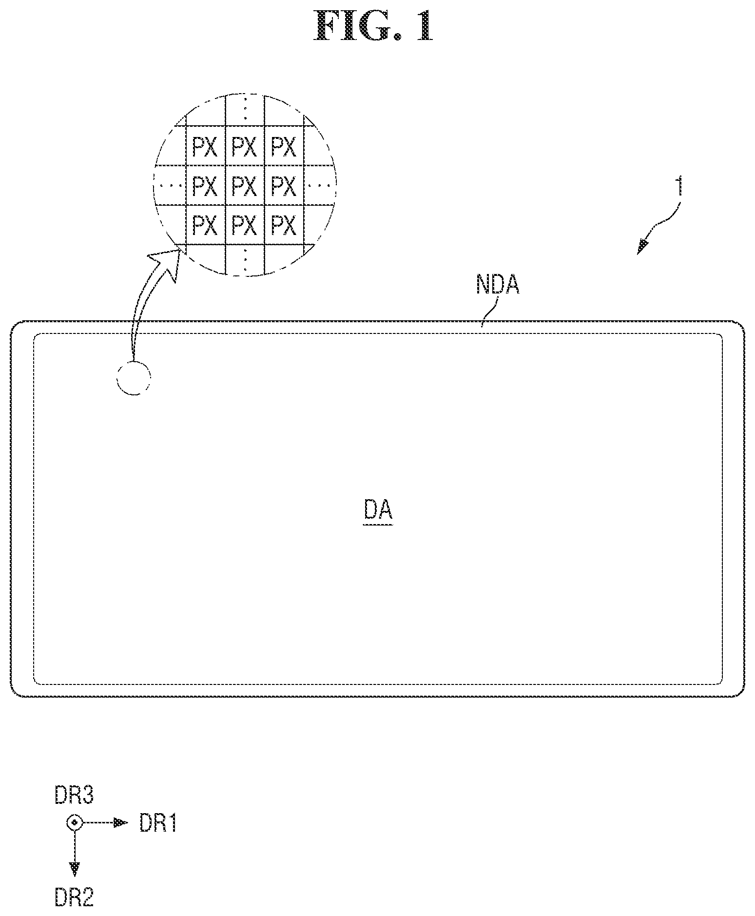
These and/or other aspects and features of embodiments of the present disclosure will become apparent and more readily appreciated from the following description of the embodiments, taken in conjunction with the accompanying drawings in which: is a schematic plan view of a display device according to one or more embodiments; is a schematic layout view illustrating a plurality of wirings of the display device according to one or more embodiments; is a pixel circuit diagram of the display device according to one or more embodiments; is a plan view illustrating the structure of a pixel of the display device according to one or more embodiments; is a perspective cutaway view illustrating the structure of a light emitting element of ; is an enlarged view of an area A 1 of ; is a plan view illustrating the structure of a first connection electrode according to one or more embodiments; is a plan view illustrating the structure of a second connection electrode according to one or more embodiments; is a plan view illustrating the structure of a fifth connection electrode according to one or more embodiments; is a schematic cross-sectional view taken along the line X 1 -X 1 ′ of ; is a schematic cross-sectional view taken along the line X 2 -X 2 ′ of ; through 14 are cross-sectional views illustrating a process of manufacturing the display device according to one or more embodiments; is a plan view illustrating the structure of a subpixel of a display device according to one or more embodiments; is a plan view illustrating the structure of a subpixel of a display device according to one or more embodiments; is a plan view illustrating the structure of a subpixel of a display device according to one or more embodiments; and is a plan view illustrating the structure of a subpixel of a display device according to one or more embodiments.
DETAILED DESCRIPTION
The present disclosure will now be described more fully hereinafter with reference to the accompanying drawings, in which embodiments of the present disclosure are shown. The present disclosure may, however, be embodied in different forms and should not be construed as limited to embodiments set forth herein. Rather, these embodiments are provided so that the present disclosure will be thorough and complete, and will fully convey the scope of the present disclosure to those skilled in the art. It will also be understood that when a layer is referred to as being “on” another layer or substrate, it can be directly on the other layer or substrate, or intervening layers may also be present. The same reference numbers indicate the same components throughout the specification. It will be understood that, although the terms “first,” “second,” etc. may be used herein to describe various elements, these elements should not be limited by these terms. These terms are only used to distinguish one element from another element. For instance, a first element discussed below could be termed a second element without departing from the teachings of the present disclosure. Similarly, the second element could also be termed the first element. Features of each of various embodiments of the present disclosure may be partially or entirely combined with each other and may technically variously interwork with each other, and respective embodiments may be implemented independently of each other or may be implemented together in association with each other. Hereinafter, specific embodiments will be described with reference to the accompanying drawings. is a schematic plan view of a display device 1 according to one or more embodiments. In , a first direction DR 1 , a second direction DR 2 , and a third direction DR 3 are defined. The first direction DR 1 and the second direction DR 2 may be perpendicular to each other, the first direction DR 1 and the third direction DR 3 may be perpendicular to each other, and the second direction DR 2 and the third direction DR 3 may be perpendicular to each other. It may be understood that the first direction DR 1 refers to a horizontal direction in the drawing, the second direction DR 2 refers to a vertical direction in the drawing, and the third direction DR 3 refers to an up-down direction in the drawing, that is, a thickness direction of the display device 1 . In the following specification, unless otherwise specified, a “direction” may refer to both directions extending to both sides along the direction. In addition, when it is necessary to distinguish both “directions” extending to both sides, a first side is referred to as a “first side in the direction,” and a second side is referred to as a “second side in the direction.” Based on , a direction in which an arrow is directed is referred to as the first side, and a direction opposite to the direction is referred to as the second side. Hereinafter, for ease of description, in referring to surfaces of the display device 1 or each member constituting the display device 1 , one surface facing the first side in a direction in which an image is displayed, that is, in the third direction DR 3 is referred to as a top surface, and a surface opposite the one surface is referred to as a bottom surface. However, the present disclosure is not limited thereto, and the one surface and the other surface of each member may also be referred to as a front surface and a rear surface or as a first surface and a second surface, respectively. In addition, in describing relative positions of the members of the display device 1 , the first side in the third direction DR 3 may be referred to as an upper side, and the second side in the third direction DR 3 may be referred to as a lower side. Referring to , the display device 1 displays moving images or still images. The display device 1 may refer to any electronic device that provides a display screen. Examples of the display device 1 may include a television, a notebook computer, a monitor, a billboard, an Internet of things (IoT) device, a mobile phone, a smartphone, a tablet personal computer (PC), an electronic watch, a smart watch, a watch phone, a head-mounted display, a mobile communication terminal, an electronic notebook, an electronic book, a portable multimedia player (PMP), a navigation device, a game console, a digital camera and a camcorder, all of which provide a display screen. The display device 1 includes a display panel that provides a display screen. Examples of the display panel may include an inorganic light emitting diode display panel, an organic light emitting display panel, a quantum dot light emitting display panel, a plasma display panel, and a field emission display panel. A case where an inorganic light emitting diode display panel is applied as an example of the display panel will be described below, but the present disclosure is not limited to this case, and other display panels can also be applied as long as the same technical spirit is applicable. The shape of the display device 1 can be variously modified. For example, the display device 1 may have various shapes such as a horizontally long rectangle, a vertically long rectangle, a square, a quadrilateral with rounded corners (or vertices), other polygons, or a circle. The shape of a display area DA of the display device 1 may also be similar to the overall shape of the display device 1 . In , the display device 1 shaped like a rectangle that is long in the first direction DR 1 is illustrated. The display device 1 may include the display area DA and a non-display area NDA around an edge or periphery of the display area DA. The display area DA may be an area where an image can be displayed, and the non-display area NDA may be an area where no image is displayed. The display area DA may also be referred to as an active area, and the non-display area NDA may also be referred to as an inactive area. The display area DA may generally occupy a center (or a central region) of the display device 1 . The display area DA may include a plurality of pixels PX. The pixels PX may be arranged in a matrix direction. For example, the pixels PX may be arranged along rows and columns of a matrix. Each of the pixels PX may be rectangular or square in a plan view. However, the present disclosure is not limited thereto, and each of the pixels PX may also have a rhombic planar shape having each side inclined with respect to a direction. The pixels PX may be arranged in a stripe or island type. In addition, each of the pixels PX may include one or more light emitting elements which emit light of a specific wavelength band to display a specific color. The non-display area NDA may be located around the display area DA. The non-display area NDA may entirely or partially surround the display area DA. The display area DA may be rectangular, and the non-display area NDA may be disposed adjacent to four sides of the display area DA. The non-display area NDA may form a bezel of the display device 1 . In each non-display area NDA, wirings or circuit drivers included in the display device 1 may be located, or external devices may be mounted. is a schematic layout view illustrating a plurality of wirings of the display device 1 according to one or more embodiments. Referring to , the display device 1 may include a plurality of wirings. The display device 1 may include a plurality of scan lines SL (SL 1 through SL 3 ), a plurality of data lines DTL (DTL 1 through DTL 3 ), initialization voltage wirings VIL, and a plurality of voltage wirings VL (VL 1 through VL 4 ). In addition, in one or more embodiments, other wirings may be further disposed in the display device 1 . The wirings may include wirings made of a first conductive layer and extending in the first direction DR 1 and wirings made of a third conductive layer and extending in the second direction DR 2 . However, the extending direction of each wiring is not limited thereto. First scan lines SL 1 and second scan lines SL 2 may extend in the second direction DR 2 . A first scan line SL 1 and a second scan line SL 2 in each pair may be disposed adjacent to each other and may be spaced from other first scan lines SL 1 and other second scan lines SL 2 in the first direction DR 1 . The first and second scan lines SL 1 and SL 2 may be connected to each scan wiring pad WPD_SC connected to a scan driver. The first scan lines SL 1 and the second scan lines SL 2 may extend from a pad area PDA disposed in the non-display area NDA to the display area DA. Each third scan line SL 3 may extend in the first direction DR 1 and may be spaced from other third scan lines SL 3 in the second direction DR 2 . One third scan line SL 3 may be connected to one or more first scan lines SL 1 or one or more second scan lines SL 2 . The scan lines SL may have a mesh structure in the entire display area DA, but the present disclosure is not limited thereto. In the present specification, the term “connect” may mean that any one member and another member are connected to each other not only through physical contact but also through another member. In addition, it can be understood that any one part and another part are connected to each other as one integrated member. Further, the connection between any one member and another member can be interpreted to include electrical connection through another member in addition to connection through direct contact. The data lines DTL may extend in the second direction DR 2 . The data lines DTL may include first data lines DTL 1 , second data lines DTL 2 , and third data lines DTL 3 . Each one of the first through third data lines DTL 1 through DTL 3 may form one group and may be disposed adjacent to each other. The data lines DTL 1 through DTL 3 may extend from the pad area PDA disposed in the non-display area NDA to the display area DA. However, the present disclosure is not limited thereto, and the data lines DTL may also be disposed at equal intervals between first and second voltage wirings VL 1 and VL 2 to be described later. The initialization voltage wirings VIL may extend in the second direction DR 2 . Each of the initialization voltage wirings VIL may be disposed between the data lines DTL and a first voltage wiring VL 1 . The initialization voltage wirings VIL may extend from the pad area PDA disposed in the non-display area NDA to the display area DA. The first voltage wirings VL 1 and the second voltage wirings VL 2 extend in the second direction DR 2 , and third voltage wirings VL 3 and fourth voltage wirings VL 4 extend in the first direction DR 1 . The first voltage wirings VL 1 and the second voltage wirings VL 2 may be alternately arranged along the first direction DR 1 , and the third voltage wirings VL 3 and the fourth voltage wirings VL 4 may be alternately arranged along the second direction DR 2 . The first voltage wirings VL 1 and the second voltage wirings VL 2 may extend in the second direction DR 2 to cross the display area DA. From among the third voltage wirings VL 3 and the fourth voltage wirings VL 4 , some wirings may be disposed in the display area DA, and other wirings may be disposed in the non-display area NDA located on both sides of the display area DA in the first direction DR 1 and the second direction DR 2 . The first voltage wirings VL 1 and the second voltage wirings VL 2 may be made of the first conductive layer, and the third voltage wirings VL 3 and the fourth voltage wirings VL 4 may be made of the third conductive layer disposed on a different layer from the first conductive layer. Each of the first voltage wirings VL 1 may be connected to at least one third voltage wiring VL 3 , and each of the second voltage wirings VL 2 may be connected to at least one fourth voltage wiring VL 4 . Therefore, the voltage wirings VL may have a mesh structure in the entire display area DA. However, the present disclosure is not limited thereto. The first scan lines SL 1 , the second scan lines SL 2 , the data lines DTL, the initialization voltage wirings VIL, the first voltage wirings VL 1 , and the second voltage wirings VL 2 may be electrically connected to at least one wiring pad WPD. Each wiring pad WPD may be disposed in the non-display area NDA. In one or more embodiments, each wiring pad WPD may be disposed in the pad area PDA located on a lower side of the display area DA, which is a first side in the second direction DR 2 . The first and second scan lines SL 1 and SL 2 are connected to each scan wiring pad WPD_SC disposed in the pad area PDA, and the data lines DTL are connected to different data wiring pads WPD_DT, respectively. Each of the initialization voltage wirings VIL is connected to an initialization wiring pad WPD_Vint, the first voltage wirings VL 1 are connected to a first voltage wiring pad WPD_VL 1 , and the second voltage wirings VL 2 are connected to a second voltage wiring pad WPD_VL 2 . An external device may be mounted on the wiring pads WPD. The external device may be mounted on the wiring pads WPD through an anisotropic conductive film, ultrasonic bonding, or the like. Although each wiring pad WPD is disposed in the pad area PDA located on the lower side of the display area DA in the drawing, the present disclosure is not limited thereto. Some of the wiring pads WPD may also be disposed in an area located on an upper side or any one of left and right sides of the display area DA. Each pixel PX or subpixel SPXn (where n is an integer of 1 to 3) of the display device 1 includes a pixel driving circuit. The above-described wirings may transmit driving signals to each pixel driving circuit while passing through or around each pixel PX. The pixel driving circuit may include a transistor and a capacitor. The number of transistors and capacitors in each pixel driving circuit can be variously changed. According to one or more embodiments, each subpixel SPXn of the display device 1 may have a 3T1C structure in which the pixel driving circuit includes three transistors and one capacitor. Although the pixel driving circuit will be described below using the 3T1C structure as an example, the present disclosure is not limited thereto, and other various modified structures such as a 2T1C structure, a 7T1C structure, and a 6T1C structure are also applicable. is a pixel circuit diagram of the display device 1 according to the embodiment. Referring to , each subpixel SPXn of the display device 1 according to one or more embodiments and includes three transistors T 1 through T 3 and one storage capacitor Cst in addition to a light emitting diode EL. The light emitting diode EL emits light according to a current supplied through a first transistor T 1 . The light emitting diode EL includes a first electrode, a second electrode, and at least one light emitting element disposed between them. The light emitting element may emit light of a specific wavelength band in response to electrical signals received from the first electrode and the second electrode. A first end of the light emitting diode EL may be connected to a source electrode of the first transistor T 1 , and a second end of the light emitting diode EL may be connected to a second voltage wiring VL 2 to which a low potential voltage (hereinafter, referred to as a second power supply voltage) lower than a high potential voltage (hereinafter, referred to as a first power supply voltage) of a first voltage wiring VL 1 is supplied. The first transistor T 1 adjusts a current flowing from the first voltage wiring VL 1 , to which the first power supply voltage is supplied, to the light emitting diode EL according to a voltage difference between a gate electrode and the source electrode of the first transistor T 1 . For example, the first transistor T 1 may be a driving transistor for driving the light emitting diode EL. The first transistor T 1 may have the gate electrode connected to a source electrode of a second transistor T 2 , the source electrode connected to the first electrode of the light emitting diode EL, and a drain electrode connected to the first voltage wiring VL 1 to which the first power supply voltage is applied. The second transistor T 2 is turned on by a scan signal of a scan line SL to connect a data line DTL to the gate electrode of the first transistor T 1 . The second transistor T 2 may have a gate electrode connected to the scan line SL, the source electrode connected to the gate electrode of the first transistor T 1 , and a drain electrode connected to the data line DTL. A third transistor T 3 is turned on by a scan signal of a scan line SL to connect an initialization voltage wiring VIL to the first end of the light emitting diode EL. The third transistor T 3 may have a gate electrode connected to the scan line SL, a drain electrode connected to the initialization voltage wiring VIL, and a source electrode connected to the first end of the light emitting diode EL or the source electrode of the first transistor T 1 . In one or more embodiments, the source electrode and the drain electrode of each of the transistors T 1 through T 3 are not limited to the above description, and the opposite may also be the case. Each of the transistors T 1 through T 3 may be formed as a thin-film transistor (TFT). Although each of the transistors T 1 through T 3 is mainly described as an N-type metal oxide semiconductor field effect transistor (MOSFET) in , the present disclosure is not limited thereto. That is, each of the transistors T 1 through T 3 may also be formed as a P-type MOSFET, or some of the transistors T 1 through T 3 may be formed as N-type MOSFETs, and the other may be formed as a P-type MOSFET. The storage capacitor Cst is formed between the gate electrode and the source electrode of the first transistor T 1 . The storage capacitor Cst stores a difference between a gate voltage and a source voltage of the first transistor T 1 . In the embodiment of , the gate electrode of the second transistor T 2 may be connected to the scan line SL, and the gate electrode of the third transistor T 3 may be connected to the scan line SL. In other words, the second transistor T 2 and the third transistor T 3 may be turned on by a scan signal transmitted from the same scan line. However, the present disclosure is not limited thereto, and the second transistor T 2 and the third transistor T 3 may also be connected to different scan lines and turned on by scan signals transmitted from different scan lines. The structure of a pixel PX of the display device 1 according to one or more embodiments will now be described. is a plan view illustrating the structure of a pixel PX of the display device 1 according to one or more embodiments. is a perspective cutaway view illustrating the structure of a light emitting element ED of . is an enlarged view of an area A 1 of . is a plan view illustrating the structure of a first connection electrode CNE 1 . is a plan view illustrating the structure of a second connection electrode CNE 2 . is a plan view illustrating the structure of a fifth connection electrode CNE 5 . illustrate the planar arrangement of alignment electrodes RME, an outer bank BNL, a plurality of light emitting elements ED, and connection electrodes CNE in a pixel PX of the display device 1 . through 9 illustrate various types of connection electrodes CNE. Referring to , each pixel PX of the display device 1 may include a plurality of subpixels SPXn. For example, one pixel PX may include a first subpixel SPX 1 , a second subpixel SPX 2 , and a third subpixel SPX 3 . The first subpixel SPX 1 may emit light of a first color, the second subpixel SPX 2 may emit light of a second color, and the third subpixel SPX 3 may emit light of a third color. For example, the first color may be blue, the second color may be green, and the third color may be red. However, the present disclosure is not limited thereto, and the subpixels SPXn may also emit light of the same color. In one or more embodiments, the subpixels SPXn may emit blue light. Although one pixel PX includes three subpixels SPXn in the drawing, the present disclosure is not limited thereto, and the pixel PX may also include a greater number of subpixels SPXn. For ease of description, a case where one pixel PX includes three subpixels SPXn will be mainly described below. The first subpixel SPX 1 , the second subpixel SPX 2 , and the third subpixel SPX 3 may be sequentially arranged along a first side in the first direction DR 1 . For example, the first subpixel SPX 1 may be disposed on a first side of the third subpixel SPX 3 in the first direction DR 1 . Accordingly, a pixel PX and at least any one of the subpixels SPXn of the pixel PX may neighbor at least any one of the subpixels SPXn of another pixel PX neighboring the pixel PX. For example, based on , the third subpixel SPX 3 of a pixel PX disposed on a second side in the first direction DR 1 may neighbor the first subpixel SPX 1 of another pixel PX adjacent to a first side, in the first direction DR 1 , of the pixel PX disposed on the second side in the first direction DR 1 . Each subpixel SPXn of the display device 1 may include an emission area EMA and a non-emission area. The emission area EMA may be an area in which the light emitting elements ED are disposed to emit light of a specific wavelength band. The non-emission area may be an area in which the light emitting elements ED are not disposed and from which no light is output because light emitted from the light emitting elements ED does not reach this area. The emission area EMA may be defined by the outer bank BNL. In other words, the emission area EMA may be a space surrounded by the outer bank BNL. The emission area EMA may have a rectangular shape including short sides in the first direction DR 1 and long sides in the second direction DR 2 in a plan view. The emission area EMA may include an area in which the light emitting elements ED are disposed and an area which is adjacent to the light emitting elements ED and from which light emitted from the light emitting elements ED is output. For example, the emission area EMA may also include an area from which light emitted from the light emitting elements ED is output after being reflected or refracted by other members. A plurality of light emitting elements ED may be disposed in each subpixel SPXn, and an area where the light emitting elements ED are located and an area adjacent to this area may form the emission area EMA. Although the respective emission areas EMA of the subpixels SPXn have the same area in the drawing, the present disclosure is not limited thereto. In one or more embodiments, the emission area EMA of each subpixel SPXn may have a different area according to the color or wavelength band of light emitted from the light emitting elements ED disposed in the subpixel SPXn. In one or more embodiments, a width of the emission area EMA in the first direction DR 1 may be, but is not limited to, approximately 74 μm. Each subpixel SPXn may further include a sub-area SA disposed in the non-emission area. The sub-area SA may be an area defined according to the arrangement of the alignment electrodes RME. The sub-area SA may be disposed on a first side and a second side of the emission area EMA of each subpixel SPXn in the second direction DR 2 . The emission area EMA may be repeatedly arranged along the first direction DR 1 , and the sub-area SA may extend in the first direction DR 1 . A plurality of emission areas EMA and a plurality of sub-areas SA may be alternately arranged along the second direction DR 2 . A plurality of emission areas EMA may be disposed between the sub-areas SA. The sub-area SA may be an area shared by subpixels SPXn adjacent to each other in the first direction DR 1 . For example, the first subpixel SPX 1 , the second subpixel SPX 2 , and the third subpixel SPX 3 may share the sub-area SA. In addition, the sub-area SA may be an area shared by subpixels SPXn adjacent to each other in the second direction DR 2 . For example, the sub-area SA disposed on both sides of the outer bank BNL in the second direction DR 2 in may be shared by the subpixels SPXn illustrated in the drawing and subpixels SPXn not illustrated in the drawing and adjacent to the subpixels SPXn in the second direction DR 2 . Light may not exit from the sub-area SA because the light emitting elements ED are not disposed in the sub-area SA, but a portion of each of the alignment electrodes RME disposed in each subpixel SPXn may be disposed in the sub-area SA. The alignment electrodes RME disposed in different subpixels SPXn may be separated from each other by a separation portion ROP of the sub-area SA. The alignment electrodes RME may include a first alignment electrode RME 1 , a second alignment electrode RME 2 , and a third alignment electrode RME 3 sequentially arranged along the first side in the first direction DR 1 in each subpixel SPXn. The first alignment electrode RME 1 , the second alignment electrode RME 2 , and the third alignment electrode RME 3 may be spaced from each other in the first direction DR 1 . Different alignment signals may be transmitted to the first alignment electrode RME 1 , the second alignment electrode RME 2 , and the third alignment electrode RME 3 in a process of manufacturing the display device 1 according to one or more embodiments that will be described later. This will be described in detail later. The first alignment electrode RME 1 may be disposed on the second side of the emission area EMA in the first direction DR 1 . For example, the first alignment electrode RME 1 may be spaced from a portion of the outer bank BNL which forms a side of the emission area EMA on the second side in the first direction DR 1 . The first alignment electrode RME 1 may extend in the second direction DR 2 . In one or more embodiments, the first alignment electrode RME 1 may have a rectangular planar profile, but the present disclosure is not limited thereto. In , the first alignment electrode RME 1 has a rectangular planar profile. The second alignment electrode RME 2 may be disposed on a first side of the first alignment electrode RME 1 in the first direction DR 1 . The second alignment electrode RME 2 may be disposed between the first alignment electrode RME 1 and the third alignment electrode RME 3 . In one or more embodiments, the second alignment electrode RME 2 may be disposed in a center of the emission area EMA, but the present disclosure is not limited thereto. The second alignment electrode RME 2 may extend in the second direction DR 2 . In one or more embodiments, the second alignment electrode RME 2 may have a rectangular planar profile, but the present disclosure is not limited thereto. In , the second alignment electrode RME 2 has a rectangular planar profile. The second alignment electrode RME 2 may be electrically connected to a circuit element layer CCL (see ), which will be described later, through a first electrode contact hole CTD. The second alignment electrode RME 2 may receive the above-described first power supply voltage through the first electrode contact hole CTD. The third alignment electrode RME 3 may be disposed on a first side of the emission area EMA in the first direction DR 1 . For example, the third alignment electrode RME 3 may be spaced from a portion of the outer bank BNL that forms a side of the emission area EMA on the first side in the first direction DR 1 . The third alignment electrode RME 3 may extend in the second direction DR 2 . In one or more embodiments, the third alignment electrode RME 3 may have a rectangular planar profile, but the present disclosure is not limited thereto. In , the third alignment electrode RME 3 has a rectangular planar profile. The third alignment electrode RME 3 may be electrically connected to the circuit element layer CCL (see ), which will be described later, through a second electrode contact hole CTS. The third alignment electrode RME 3 may receive the above-described second power supply voltage through the second electrode contact hole CTS. The first electrode contact hole CTD and the second electrode contact hole CTS may not overlap the emission area EMA. In one or more embodiments, the first electrode contact hole CTD and the second electrode contact hole CTS may overlap the outer bank BNL, but the present disclosure is not limited thereto. For example, the first electrode contact hole CTD and the second electrode contact hole CTS may be disposed in the sub-area SA. In , the first electrode contact hole CTD and the second electrode contact hole CTS overlap the outer bank BNL. As illustrated in , a plurality of inner banks BP may be disposed under the alignment electrodes RME, respectively. The inner banks BP may be disposed in the emission area EMA of each subpixel SPXn. The inner banks BP may include a first inner bank BP 1 , a second inner bank BP 2 , and a third inner bank BP 3 , each having a rectangular planar shape extending in the second direction DR 2 . The first inner bank BP 1 , the second inner bank BP 2 , and the third inner bank BP 3 may be spaced from each other in the first direction DR 1 . The first inner bank BP 1 may be disposed under the first alignment electrode RME 1 in the emission area EMA, the second inner bank BP 2 may be disposed under the second alignment electrode RME 2 in the emission area EMA, and the third inner bank BP 3 may be disposed under the third alignment electrode RME 3 in the emission area EMA. In one or more embodiments, the alignment electrodes RME may completely cover the inner banks BP respectively disposed under the alignment electrodes RME in the emission area EMA, but the present disclosure is not limited thereto. For example, the alignment electrodes RME may partially cover the inner banks BP respectively disposed under the alignment electrodes RME in the emission area EMA. In , the alignment electrodes RME completely cover the inner banks BP respectively disposed under the alignment electrodes RME in the emission area EMA. The alignment electrodes RME may be spaced from each other in the first direction DR 1 to provide a space in which the light emitting elements ED are disposed. For example, the light emitting elements ED may be disposed in a space between the first alignment electrode RME 1 and the second alignment electrode RME 2 and a space between the second alignment electrode RME 2 and the third alignment electrode RME 3 . Referring to , a light emitting element ED may be a light emitting diode. Specifically, the light emitting element ED may be an inorganic light emitting diode having a size of nanometers to micrometers and made of an inorganic material. When an electric field is formed in a specific direction between two electrodes facing each other, the light emitting element ED may be aligned between the two electrodes in which polarities are formed. The light emitting element ED according to one or more embodiments may extend in one direction. The light emitting element ED may be shaped like a cylinder, a rod, a wire, a tube, or the like. However, the shape of the light emitting element ED is not limited thereto, and the light emitting element ED may also have various shapes including polygonal prisms, such as a cube, a rectangular parallelepiped or a hexagonal prism, and a shape extending in a direction and having a partially inclined outer surface. The light emitting element ED may include a semiconductor layer doped with a dopant of any conductivity type (e.g., a p-type or an n-type). The semiconductor layer may receive an electrical signal from an external power source and emit light of a specific wavelength band. The light emitting element ED may include a first semiconductor layer 31 , a second semiconductor layer 32 , a light emitting layer 36 , an electrode layer 37 , and an insulating film 38 . The first semiconductor layer 31 may be an n-type semiconductor. The first semiconductor layer 31 may include a semiconductor material having a chemical formula of Al x Ga y In 1-x-y N (0≤x≤1, 0≤y≤1, 0≤x+y≤1). For example, the first semiconductor layer 31 may be one or more selected from among AlGaInN, GaN, AlGaN, InGaN, AlN, and InN doped with an n-type dopant. The n-type dopant used to dope the first semiconductor layer 31 may be Si, Ge, Sn, or the like. The second semiconductor layer 32 is disposed on the first semiconductor layer 31 with the light emitting layer 36 interposed between them. The second semiconductor layer 32 may be a p-type semiconductor. The second semiconductor layer 32 may include a semiconductor material having a chemical formula of Al x Ga y In 1-x-y N (0≤x≤1, 0≤y≤1, 0≤x+y≤1). For example, the second semiconductor layer 32 may be one or more selected from among AlGaInN, GaN, AlGaN, InGaN, AlN, and InN doped with a p-type dopant. The p-type dopant used to dope the second semiconductor layer 32 may be Mg, Zn, Ca, Ba, or the like. Accordingly, ends of the light emitting element ED may have different polarities from each other. For ease of description, one end adjacent to the second semiconductor layer 32 from among the ends of the light emitting element ED will hereinafter be referred to as a “first end,” and the other end adjacent to the first semiconductor layer 31 will hereinafter be referred to as a “second end”. The first end of the light emitting element ED may be located opposite the second end. The first end and the second end of the light emitting element ED may have different polarities. For example, first ends of different light emitting elements ED may have the same polarity, and second ends of different light emitting elements ED may have the same polarity. Although each of the first semiconductor layer 31 and the second semiconductor layer 32 is composed of one layer in the drawing, the present disclosure is not limited thereto. Each of the first semiconductor layer 31 and the second semiconductor layer 32 may also include more layers, for example, may further include a clad layer or a tensile strain barrier reducing (TSBR) layer depending on the material of the light emitting layer 36 . For example, the light emitting element ED may further include another semiconductor layer disposed between the first semiconductor layer 31 and the light emitting layer 36 or between the second semiconductor layer 32 and the light emitting layer 36 . The semiconductor layer disposed between the first semiconductor layer 31 and the light emitting layer 36 may be one or more selected from among AlGaInN, GaN, AlGaN, InGaN, AlN, InN, and SLs doped with an n-type dopant. The semiconductor layer disposed between the second semiconductor layer 32 and the light emitting layer 36 may be one or more selected from among AlGaInN, GaN, AlGaN, InGaN, AlN, and InN doped with a p-type dopant. The light emitting layer 36 is disposed between the first semiconductor layer 31 and the second semiconductor layer 32 . The light emitting layer 36 may include a material having a single or multiple quantum well structure. When the light emitting layer 36 includes a material having a multiple quantum well structure, it may have a structure in which a plurality of quantum layers and a plurality of well layers are alternately stacked. The light emitting layer 36 may emit light through combination of electron-hole pairs according to electrical signals received through the first semiconductor layer 31 and the second semiconductor layer 32 . The light emitting layer 36 may include a material such as AlGaN, AlGaInN, or InGaN. In particular, when the light emitting layer 36 has a multiple quantum well structure in which a quantum layer and a well layer are alternately stacked, the quantum layer may include a material such as AlGaN or AlGaInN, and the well layer may include a material such as GaN or AlInN. The light emitting layer 36 may also have a structure in which a semiconductor material having a large band gap energy and a semiconductor material having a small band gap energy are alternately stacked or may include different Group III to V semiconductor materials depending on the wavelength band of light that it emits. Light emitted from the light emitting layer 36 is not limited to light in a blue wavelength band. In some cases, the light emitting layer 36 may emit light in a red or green wavelength band. The electrode layer 37 may be an ohmic connection electrode. However, the present disclosure is not limited thereto, and the electrode layer 37 may also be a Schottky connection electrode. The light emitting element ED may include at least one electrode layer 37 . The light emitting element ED may include one or more electrode layers 37 . However, the present disclosure is not limited thereto, and the electrode layer 37 may also be omitted. When the light emitting element ED is electrically connected to electrodes or connection electrodes in the display device 1 , the electrode layer 37 may reduce the resistance between the light emitting element ED and the electrodes or the connection electrodes. The electrode layer 37 may include a conductive metal. For example, the electrode layer 37 may include at least one selected from among aluminum (Al), titanium (Ti), indium (In), gold (Au), silver (Ag), indium tin oxide (ITO), indium zinc oxide (IZO), and indium tin zinc oxide (ITZO). Both ends of each light emitting element ED configured as described above may have different polarities. The insulating film 38 may be around (e.g., may surround) outer surfaces (e.g., outer peripheral or circumferential surfaces) of the semiconductor layers and the electrode layer described above. For example, the insulating film 38 may be around (e.g., may surround) an outer surface (e.g., an outer peripheral or circumferential surface) of at least the light emitting layer 36 but may expose both ends of the light emitting element ED in a longitudinal direction. In addition, an upper surface of the insulating film 38 may be rounded in cross section in an area adjacent to at least one end of the light emitting element ED. The insulating film 38 may include an insulating material, for example, at least one selected from among silicon oxide (SiO x ), silicon nitride (SiN x ), silicon oxynitride (SiO x N y ), aluminum nitride (AlN x ), aluminum oxide (AlO x ), zirconium oxide (ZrO x ), hafnium oxide (HfO x ), and titanium oxide (TiO x ). Although the insulating film 38 is illustrated as a single layer in the drawing, the present disclosure is not limited thereto. In one or more embodiments, the insulating film 38 may be formed in a multilayer structure in which a plurality of layers are stacked. The insulating film 38 may protect the semiconductor layers and the electrode layer of the light emitting element ED. The insulating film 38 may prevent an electrical short circuit that may occur in the light emitting layer 36 when the light emitting layer 36 directly contacts an electrode that transmits an electrical signal to the light emitting element ED. In addition, the insulating film 38 may prevent a reduction in luminous efficiency of the light emitting element ED. In addition, an outer surface (e.g., an outer peripheral or circumferential surface) of the insulating film 38 may be treated. The light emitting element ED may be sprayed onto electrodes in a state where it is dispersed in ink (e.g., a predetermined ink) and then may be aligned. Here, the surface of the insulating film 38 may be hydrophobic or hydrophilic-treated so that the light emitting element ED is kept separate in the ink without being agglomerated with other adjacent light emitting elements ED. Referring back to , the light emitting elements ED may include first light emitting elements ED 1 disposed in a first lane EA 1 of the emission area EMA of each subpixel SPXn, second light emitting elements ED 2 disposed in a second lane EA 2 , third light emitting elements ED 3 disposed in a third lane EA 3 , and fourth light emitting elements ED 4 disposed in a fourth lane EA 4 . Each of the first lane EA 1 , the second lane EA 2 , the third lane EA 3 , and the fourth lane EA 4 may include a first portion disposed in the space between the first alignment electrode RME 1 and the second alignment electrode RME 2 and a second portion disposed in the space between the second alignment electrode RME 2 and the third alignment electrode RME 3 . The first portion and the second portion may extend in the second direction DR 2 and may be spaced from each other in the first direction DR 1 . For example, the first lane EA 1 may include a first portion EA 1 a disposed in the space between the first alignment electrode RME 1 and the second alignment electrode RME 2 and extending in the second direction DR 2 and a second portion EA b disposed in the space between the second alignment electrode RME 2 and the third alignment electrode RME 3 and extending in the second direction DR 2 , respectively. The second lane EA 2 may include a first portion EA 2 a disposed in the space between the first alignment electrode RME 1 and the second alignment electrode RME 2 and extending in the second direction DR 2 and a second portion EA 2 b disposed in the space between the second alignment electrode RME 2 and the third alignment electrode RME 3 and extending in the second direction DR 2 , respectively. The third lane EA 3 may include a first portion EA 3 a disposed in the space between the first alignment electrode RME 1 and the second alignment electrode RME 2 and extending in the second direction DR 2 and a second portion EA 3 b disposed in the space between the second alignment electrode RME 2 and the third alignment electrode RME 3 and extending in the second direction DR 2 , respectively. The fourth lane EA 4 may include a first portion EA 4 a disposed in the space between the first alignment electrode RME 1 and the second alignment electrode RME 2 and extending in the second direction DR 2 and a second portion EA 4 b disposed in the space between the second alignment electrode RME 2 and the third alignment electrode RME 3 and extending in the second direction DR 2 , respectively. The first lane EA 1 , the second lane EA 2 , the third lane EA 3 , and the fourth lane EA 4 may be spaced from each other in the second direction DR 2 and may be sequentially arranged along the first side in the second direction DR 2 . For example, the first portion EA a of the first lane EA 1 , the first portion EA 2 a of the second lane EA 2 , the first portion EA 3 a of the third lane EA 3 , and the first portion EA 4 a of the fourth lane EA 4 may be spaced from each other in the second direction DR 2 . The second portion EA b of the first lane EA 1 , the second portion EA 2 b of the second lane EA 2 , the second portion EA 3 b of the third lane EA 3 , and the second portion EA 4 b of the fourth lane EA 4 may be spaced from each other in the second direction DR 2 . Each of the light emitting elements ED illustrated in , that is, each of the first light emitting elements ED 1 , the second light emitting elements ED 2 , the third light emitting elements ED 3 , and the fourth light emitting elements ED 4 may include a hatched portion. The hatched portion in each of the light emitting elements ED may be the light emitting layer 36 illustrated in . Accordingly, an end adjacent to the hatched portion of each of the first light emitting elements ED 1 , the second light emitting elements ED 2 , the third light emitting elements ED 3 , and the fourth light emitting elements ED 4 may be the first end described above, and the opposite end may be the second end. The first light emitting elements ED 1 may be disposed in at least any one of the first portion EA a and the second portion EA b of the first lane EA 1 . The first light emitting elements ED 1 disposed in the first portion EA a of the first lane EA 1 may extend in the first direction DR 1 and may be oriented such that the first ends thereof are disposed on a second side of the second alignment electrode RME 2 in the first direction DR 1 and the second ends are disposed on a first side of the first alignment electrode RME 1 in the first direction DR 1 . The first light emitting elements ED 1 disposed in the second portion EA b of the first lane EA 1 may extend in the first direction DR 1 and may be oriented such that the first ends thereof are disposed on a first side of the second alignment electrode RME 2 in the first direction DR 1 and the second ends are disposed on a second side of the third alignment electrode RME 3 in the first direction DR 1 . That is, the orientation of the first light emitting elements ED 1 disposed in the first portion EA a of the first lane EA 1 may be the reverse of the orientation of the first light emitting elements ED 1 disposed in the second portion EA b of the first lane EA 1 . It may be understood that the orientation of the light emitting elements ED described herein is distinguished according to the relative position of the first ends or the second ends of the light emitting elements ED. For example, in the display device 1 according to one or more embodiments, the first light emitting elements ED 1 disposed in the first portion EA a of the first lane EA 1 have the first ends facing the first side in the first direction DR 1 and the second ends facing the second side in the first direction DR 1 . On the other hand, the first light emitting elements ED 1 disposed in the second portion EA b of the first lane EA 1 have the first ends facing the second side in the first direction DR 1 and the second ends facing the first side in the first direction DR 1 . Therefore, it may be understood that the first light emitting elements ED 1 disposed in the first portion EA a and the second portion EA b of the first lane EA 1 have opposite orientations. A plurality of first light emitting elements ED 1 may be arranged side by side along the second direction DR 2 to form a group in the first lane EA 1 . For example, the first light emitting elements ED 1 may be arranged side by side along the second direction DR 2 to form a first group as a column in the first portion EA 1 a of the first lane EA 1 and may be arranged side by side along the second direction DR 2 to form a second group as a column in the second portion EA b of the first lane EA 1 . The first ends of the first group of the first light emitting elements ED 1 and the first ends of the second group of the first light emitting elements ED 1 may be electrically connected by connection electrodes CNE. That is, the first group and the second group of the first light emitting elements ED 1 may be connected in parallel. The second light emitting elements ED 2 may be disposed in at least any one of the first portion EA 2 a and the second portion EA 2 b of the second lane EA 2 . The second light emitting elements ED 2 disposed in the first portion EA 2 a of the second lane EA 2 may extend in the first direction DR 1 and may be oriented such that the first ends thereof are disposed on the second side of the second alignment electrode RME 2 in the first direction DR 1 and the second ends are disposed on the first side of the first alignment electrode RME 1 in the first direction DR 1 . The second light emitting elements ED 2 disposed in the second portion EA 2 b of the second lane EA 2 may extend in the first direction DR 1 and may be oriented such that the first ends thereof are disposed on the first side of the second alignment electrode RME 2 in the first direction DR 1 and the second ends are disposed on the second side of the third alignment electrode RME 3 in the first direction DR 1 . That is, the orientation of the second light emitting elements ED 2 disposed in the first portion EA 2 a of the second lane EA 2 may be the reverse of the orientation of the second light emitting elements ED 2 disposed in the second portion EA 2 b of the second lane EA 2 . A plurality of second light emitting elements ED 2 may be arranged side by side along the second direction DR 2 to form a group in the second lane EA 2 . For example, the second light emitting elements ED 2 may be arranged side by side in the second direction DR 2 to form a first group as a column in the first portion EA 2 a of the second lane EA 2 and may be arranged side by side along the second direction DR 2 to form a second group as a column in the second portion EA 2 b of the second lane EA 2 . The first ends of the first group of the second light emitting elements ED 2 and the first ends of the second group of the second light emitting elements ED 2 may be electrically connected by the connection electrodes CNE. That is, the first group and the second group of the second light emitting elements ED 2 may be connected in parallel. The third light emitting elements ED 3 may be disposed in at least any one of the first portion EA 3 a and the second portion EA 3 b of the third lane EA 3 . The third light emitting elements ED 3 disposed in the first portion EA 3 a of the third lane EA 3 may extend in the first direction DR 1 and may be oriented such that the first ends thereof are disposed on the second side of the second alignment electrode RME 2 in the first direction DR 1 and the second ends are disposed on the first side of the first alignment electrode RME 1 in the first direction DR 1 . The third light emitting elements ED 3 disposed in the second portion EA 3 b of the third lane EA 3 may extend in the first direction DR 1 and may be oriented such that the first ends thereof are disposed on the first side of the second alignment electrode RME 2 in the first direction DR 1 and the second ends are disposed on the second side of the third alignment electrode RME 3 in the first direction DR 1 . That is, the orientation of the third light emitting elements ED 3 disposed in the first portion EA 3 a of the third lane EA 3 may be the reverse of the orientation of the third light emitting elements ED 3 disposed in the second portion EA 3 b of the third lane EA 3 . A plurality of third light emitting elements ED 3 may be arranged side by side along the second direction DR 2 to form a group in the third lane EA 3 . For example, the third light emitting elements ED 3 may be arranged side by side along the second direction DR 2 to form a first group as a column in the first portion EA 3 a of the third lane EA 3 and may be arranged side by side along the second direction DR 2 to form a second group as a column in the second portion EA 3 b of the third lane EA 3 . The first ends of the first group of the third light emitting elements ED 3 and the first ends of the second group of the third light emitting elements ED 3 may be electrically connected by the connection electrodes CNE. That is, the first group and the second group of the third light emitting elements ED 3 may be connected in parallel. The fourth light emitting elements ED 4 may be disposed in at least any one of the first portion EA 4 a and the second portion EA 4 b of the fourth lane EA 4 . The fourth light emitting elements ED 4 disposed in the first portion EA 4 a of the fourth lane EA 4 may extend in the first direction DR 1 and may be oriented such that the first ends thereof are disposed on the second side of the second alignment electrode RME 2 in the first direction DR 1 and the second ends are disposed on the first side of the first alignment electrode RME 1 in the first direction DR 1 . The fourth light emitting elements ED 4 disposed in the second portion EA 4 b of the fourth lane EA 4 may extend in the first direction DR 1 and may be oriented such that the first ends thereof are disposed on the first side of the second alignment electrode RME 2 in the first direction DR 1 and the second ends are disposed on the second side of the third alignment electrode RME 3 in the first direction DR 1 . That is, the orientation of the fourth light emitting elements ED 4 disposed in the first portion EA 4 a of the fourth lane EA 4 may be the reverse of the orientation of the fourth light emitting elements ED 4 disposed in the second portion EA 4 b of the fourth lane EA 4 . A plurality of fourth light emitting elements ED 4 may be arranged side by side along the second direction DR 2 to form a group in the fourth lane EA 4 . For example, the fourth light emitting elements ED 4 may be arranged side by side along the second direction DR 2 to form a first group as a column in the first portion EA 4 a of the fourth lane EA 4 and may be arranged side by side along the second direction DR 2 to form a second group as a column in the second portion EA 4 b of the fourth lane EA 4 . The first ends of the first group of the fourth light emitting elements ED 4 and the first ends of the second group of the fourth light emitting elements ED 4 may be electrically connected by the connection electrodes CNE. That is, the first group and the second group of the fourth light emitting elements ED 4 may be connected in parallel. The first lane EA 1 , the second lane EA 2 , the third lane EA 3 , and the fourth lane EA 4 may be defined according to the arrangement of the connection electrodes CNE. The connection electrodes CNE may be disposed on the light emitting elements ED. The connection electrodes CNE may include a first connection electrode CNE 1 , a second connection electrode CNE 2 , a third connection electrode CNE 3 , a fourth connection electrode CNE 4 , and a fifth connection electrode CNE 5 spaced from each other in the second direction DR 2 . Referring to through 9 , the connection electrodes CNE may have various types of shapes. For example, the first connection electrode CNE 1 may have a first type shape as illustrated in , the second connection electrode CNE 2 , the third connection electrode CNE 3 , and the fourth connection electrode CNE 4 may have a second type shape as illustrated in , and the fifth connection electrode CNE 5 may have a third type shape as illustrated in . Although the second connection electrode CNE 2 is illustrated as having the second type shape in , the third connection electrode CNE 3 and the fourth connection electrode CNE 4 may also have the second type shape, that is, may have substantially the same shape as the second connection electrode CNE 2 . Referring to , the first connection electrode CNE 1 may have the first type shape branching to both sides in the first direction DR 1 on the first side in the second direction DR 2 . The first connection electrode CNE 1 may contact the first ends of the first light emitting elements ED 1 disposed in the first lane EA 1 . The first connection electrode CNE 1 may include a first power contact portion CNE 1 a , a first electrode portion CNE 1 b , a second electrode portion CNE 1 c , and a branch portion CNE 1 d . The first connection electrode CNE 1 may be referred to as a second type connection electrode in the claims. The first power contact portion CNE 1 a of the first connection electrode CNE 1 may generally extend in the second direction DR 2 . The first power contact portion CNE 1 a may extend across the outer bank BNL to the sub-area SA. The first power contact portion CNE 1 a may be electrically connected to the second alignment electrode RME 2 through a first contact portion CT 1 . Because the first power supply voltage is applied to the second alignment electrode RME 2 as described above, the first power supply voltage may also be applied to the first connection electrode CNE 1 . Accordingly, the first power supply voltage may be applied to the first ends of the first light emitting elements ED 1 arranged in the first lane EA 1 . In one or more embodiments, the first contact portion CT 1 may be disposed in the sub-area SA, but the present disclosure is not limited thereto. The branch portion CNE 1 d of the first connection electrode CNE 1 may be disposed on a first side of the first power contact portion CNE 1 a in the second direction DR 2 and may generally extend in the first direction DR 1 . Because the first power contact portion CNE 1 a is disposed in the middle of the branch portion CNE 1 d in the first direction DR 1 , the branch portion CNE 1 d may branch from the first power contact portion CNE 1 a to both sides in the first direction DR 1 . The first electrode portion CNE 1 b of the first connection electrode CNE 1 may extend from a second side of the branch portion CNE 1 d in the first direction DR 1 toward the first side in the second direction DR 2 . The first electrode portion CNE 1 b may be disposed on the second side of the second alignment electrode RME 2 in the first direction DR 1 to contact the first ends of the first light emitting element ED 1 arranged in the first portion EA 1 a of the first lane EA 1 . The second electrode portion CNE 1 c of the first connection electrode CNE 1 may extend from a first side of the branch portion CNE 1 d in the first direction DR 1 toward the first side in the second direction DR 2 . The second electrode portion CNE 1 c may be disposed on the first side of the second alignment electrode RME 2 in the first direction DR 1 to contact the first ends of the first light emitting elements ED 1 arranged in the second portion EA b of the first lane EA 1 . The first electrode portion CNE 1 b and the second electrode portion CNE 1 c may be spaced from each other in the first direction DR 1 . For example, the first electrode portion CNE 1 b and the second electrode portion CNE 1 c may be spaced from each other by a first width w 1 in the first direction DR 1 . In one or more embodiments, the first width w 1 may be smaller than a width of the second alignment electrode RME 2 in the first direction DR 1 . Referring to , the second connection electrode CNE 2 , the third connection electrode CNE 3 , and the fourth connection electrode CNE 4 may have the second type shape branching to both sides in the first direction DR 1 on the first side in the second direction DR 2 and the second side in the second direction DR 2 . The second connection electrode CNE 2 , the third connection electrode CNE 3 , and the fourth connection electrode CNE 4 may be referred to as first type connection electrodes in the claims. The second connection electrode CNE 2 may contact the second ends of the first light emitting elements ED 1 disposed in the first lane EA 1 and the first ends of the second light emitting elements ED 2 disposed in the second lane EA 2 . The second connection electrode CNE 2 may include a first electrode portion CNE 2 a , a second electrode portion CNE 2 b , a third electrode portion CNE 2 c , a fourth electrode portion CNE 2 d , and a middle portion CNE 2 e. The middle portion CNE 2 e of the second connection electrode CNE 2 may extend in the first direction DR 1 within the emission area EMA. At least a portion of the middle portion CNE 2 e may face the first electrode portion CNE 1 b and the second electrode portion CNE 1 c of the first connection electrode CNE 1 in the second direction DR 2 . A width of the middle portion CNE 2 e in the first direction DR 1 may be greater than the first width w 1 between the first electrode portion CNE 1 b and the second electrode portion CNE 1 c of the first connection electrode CNE 1 . The first electrode portion CNE 2 a of the second connection electrode CNE 2 may extend in the second direction DR 2 from a second side of the middle portion CNE 2 e in the first direction DR 1 toward the second side in the second direction DR 2 . The first electrode portion CNE 2 a may contact the second ends of the first light emitting elements ED 1 arranged in the first portion EA a of the first lane EA 1 . The second electrode portion CNE 2 b of the second connection electrode CNE 2 may extend in the second direction DR 2 from a first side of the middle portion CNE 2 e in the first direction DR 1 toward the second side in the second direction DR 2 . The second electrode portion CNE 2 b may contact the second ends of the first light emitting elements ED 1 arranged in the second portion EA b of the first lane EA 1 . The first electrode portion CNE 2 a and the second electrode portion CNE 2 b of the second connection electrode CNE 2 may be spaced from each other by a second width w 2 in the first direction DR 1 . The second width w 2 may be greater than the first width w 1 between the first electrode portion CNE 1 b and the second electrode portion CNE 1 c of the first connection electrode CNE 1 . Accordingly, the first electrode portion CNE 1 b and the second electrode portion CNE 1 c of the first connection electrode CNE 1 may be disposed in a space between the first electrode portion CNE 2 a and the second electrode portion CNE 2 b of the second connection electrode CNE 2 . For example, the first electrode portion CNE 2 a of the second connection electrode CNE 2 may face the first electrode portion CNE 1 b of the first connection electrode CNE 1 in the first direction DR 1 , and the second electrode portion CNE 2 b of the second connection electrode CNE 2 may face the second electrode portion CNE 1 c of the first connection electrode CNE 1 in the first direction DR 1 . The third electrode portion CNE 2 c of the second connection electrode CNE 2 may extend in the second direction DR 2 from the second side of the middle portion CNE 2 e in the first direction DR 1 toward the first side in the second direction DR 2 . The third electrode portion CNE 2 c may contact the first ends of the second light emitting elements ED 2 arranged in the first portion EA 2 a of the second lane EA 2 . The fourth electrode portion CNE 2 d of the second connection electrode CNE 2 may extend in the second direction DR 2 from the first side of the middle portion CNE 2 e in the first direction DR 1 toward the first side in the second direction DR 2 . The fourth electrode portion CNE 2 d may contact the first ends of the second light emitting element ED 2 arranged in the second portion EA 2 b of the second lane EA 2 . The third electrode portion CNE 2 c and the fourth electrode portion CNE 2 d of the second connection electrode CNE 2 may be spaced from each other by a third width w 3 in the first direction DR 1 . The third width w 3 may be smaller than the second width w 2 . In one or more embodiments, the third width w 3 may be substantially equal to the first width w 1 , but the present disclosure is not limited thereto. A space between the third electrode portion CNE 2 c and the fourth electrode portion CNE 2 d may overlap the space between the first electrode portion CNE 2 a and the second electrode portion CNE 2 b in the second direction DR 2 . For example, the third electrode portion CNE 2 c and the fourth electrode portion CNE 2 d may overlap the space between the first electrode portion CNE 2 a and the second electrode portion CNE 2 b in the second direction DR 2 . The third connection electrode CNE 3 may contact the second ends of the second light emitting elements ED 2 disposed in the second lane EA 2 and the first ends of the third light emitting elements ED 3 disposed in the third lane EA 3 . The third connection electrode CNE 3 may include a first electrode portion CNE 3 a , a second electrode portion CNE 3 b , a third electrode portion CNE 3 c , a fourth electrode portion CNE 3 d , and a middle portion CNE 3 e. The middle portion CNE 3 e of the third connection electrode CNE 3 may extend in the first direction DR 1 within the emission area EMA. At least a portion of the middle portion CNE 3 e may face the third electrode portion CNE 2 c and the fourth electrode portion CNE 2 d of the second connection electrode CNE 2 in the second direction DR 2 . A width of the middle portion CNE 3 e in the first direction DR 1 may be greater than the third width w 3 between the third electrode portion CNE 2 c and the fourth electrode portion CNE 2 d of the second connection electrode CNE 2 . The first electrode portion CNE 3 a of the third connection electrode CNE 3 may extend in the second direction DR 2 from a second side of the middle portion CNE 3 e in the first direction DR 1 toward the second side in the second direction DR 2 . The first electrode portion CNE 3 a may contact the second ends of the second light emitting elements ED 2 arranged in the first portion EA 2 a of the second lane EA 2 . The second electrode portion CNE 3 b of the third connection electrode CNE 3 may extend from a first side of the middle portion CNE 3 e in the first direction DR 1 toward the second side in the second direction DR 2 . The second electrode portion CNE 3 b may contact the second ends of the second light emitting elements ED 2 arranged in the second portion EA 2 b of the second lane EA 2 . The first electrode portion CNE 3 a and the second electrode portion CNE 3 b of the third connection electrode CNE 3 may be spaced from each other by the second width w 2 in the first direction DR 1 , like those of the second connection electrode CNE 2 . The second width w 2 may be greater than the third width w 3 between the third electrode portion CNE 2 c and the fourth electrode portion CNE 2 d of the second connection electrode CNE 2 . Accordingly, the third electrode portion CNE 2 c and the fourth electrode portion CNE 2 d of the second connection electrode CNE 2 may be disposed in a space between the first electrode portion CNE 3 a and the second electrode portion CNE 3 b of the third connection electrode CNE 3 . For example, the first electrode portion CNE 3 a of the third connection electrode CNE 3 may face the third electrode portion CNE 2 c of the second connection electrode CNE 2 in the first direction DR 1 , and the second electrode portion CNE 3 b of the third connection electrode CNE 3 may face the fourth electrode portion CNE 2 d of the second connection electrode CNE 2 in the first direction DR 1 . The third electrode portion CNE 3 c of the third connection electrode CNE 3 may extend in the second direction DR 2 from the second side of the middle portion CNE 3 e in the first direction DR 1 toward the first side in the second direction DR 2 . The third electrode portion CNE 3 c may contact the first ends of the third light emitting elements ED 3 arranged in the first portion EA 3 a of the third lane EA 3 . The fourth electrode portion CNE 3 d of the third connection electrode CNE 3 may extend in the second direction DR 2 from the first side of the middle portion CNE 3 e in the first direction DR 1 toward the first side in the second direction DR 2 . The fourth electrode portion CNE 3 d may contact the first ends of the third light emitting elements ED 3 arranged in the second portion EA 3 b of the third lane EA 3 . The third electrode portion CNE 3 c and the fourth electrode portion CNE 3 d of the third connection electrode CNE 3 may be spaced from each other by the third width w 3 in the first direction DR 1 , like those of the second connection electrode CNE 2 . The third width w 3 may be smaller than the second width w 2 . In one or more embodiments, the third width w 3 may be substantially equal to the first width w 1 , but the present disclosure is not limited thereto. A space between the third electrode portion CNE 3 c and the fourth electrode portion CNE 3 d may overlap the space between the first electrode portion CNE 3 a and the second electrode portion CNE 3 b in the second direction DR 2 . For example, the third electrode portion CNE 3 c and the fourth electrode portion CNE 3 d may overlap the space between the first electrode portion CNE 3 a and the second electrode portion CNE 3 b in the second direction DR 2 . The fourth connection electrode CNE 4 may contact the second ends of the third light emitting elements ED 3 disposed in the third lane EA 3 and the first ends of the fourth light emitting elements ED 4 disposed in the fourth lane EA 4 . The fourth connection electrode CNE 4 may include a first electrode portion CNE 4 a , a second electrode portion CNE 4 b , a third electrode portion CNE 4 c , a fourth electrode portion CNE 4 d , and a middle portion CNE 4 e. The middle portion CNE 4 e of the fourth connection electrode CNE 4 may extend in the first direction DR 1 within the emission area EMA. At least a portion of the middle portion CNE 4 e may face the third electrode portion CNE 3 c and the fourth electrode portion CNE 3 d of the third connection electrode CNE 3 in the second direction DR 2 . A width of the middle portion CNE 4 e in the first direction DR 1 may be greater than the third width w 3 between the third electrode portion CNE 3 c and the fourth electrode portion CNE 3 d of the third connection electrode CNE 3 . The first electrode portion CNE 4 a of the fourth connection electrode CNE 4 may extend in the second direction DR 2 from a second side of the middle portion CNE 4 e in the first direction DR 1 toward the second side in the second direction DR 2 . The first electrode portion CNE 4 a may contact the second ends of the third light emitting elements ED 3 arranged in the first portion EA 3 a of the third lane EA 3 . The second electrode portion CNE 4 b of the fourth connection electrode CNE 4 may extend in the second direction DR 2 from a first side of the middle portion CNE 4 e in the first direction DR 1 toward the second side in the second direction DR 2 . The second electrode portion CNE 4 b may contact the second ends of the third light emitting elements ED 3 arranged in the second portion EA 3 b of the third lane EA 3 . The first electrode portion CNE 4 a and the second electrode portion CNE 4 b of the fourth connection electrode CNE 4 may be spaced from each other by the second width w 2 in the first direction DR 1 , like those of the second connection electrode CNE 2 . The second width w 2 may be greater than the third width w 3 between the third electrode portion CNE 3 c and the fourth electrode portion CNE 3 d of the third connection electrode CNE 3 . Accordingly, the third electrode portion CNE 3 c and the fourth electrode portion CNE 3 d of the third connection electrode CNE 3 may be disposed in a space between the first electrode portion CNE 4 a and the second electrode portion CNE 4 b of the fourth connection electrode CNE 4 . For example, the first electrode portion CNE 4 a of the fourth connection electrode CNE 4 may face the third electrode portion CNE 3 c of the third connection electrode CNE 3 in the first direction DR 1 , and the second electrode portion CNE 4 b of the fourth connection electrode CNE 4 may face the fourth electrode portion CNE 3 d of the third connection electrode CNE 3 in the first direction DR 1 . The third electrode portion CNE 4 c of the fourth connection electrode CNE 4 may extend in the second direction DR 2 from the second side of the middle portion CNE 4 e in the first direction DR 1 toward the first side in the second direction DR 2 . The third electrode portion CNE 4 c may contact the first ends of the fourth light emitting elements ED 4 arranged in the first portion EA 4 a of the fourth lane EA 4 . The fourth electrode portion CNE 4 d of the fourth connection electrode CNE 4 may extend in the second direction DR 2 from the first side of the middle portion CNE 4 e in the first direction DR 1 toward the first side in the second direction DR 2 . The fourth electrode portion CNE 4 d may contact the first ends of the fourth light emitting elements ED 4 arranged in the second portion EA 4 b of the fourth lane EA 4 . The third electrode portion CNE 4 c and the fourth electrode portion CNE 4 d of the fourth connection electrode CNE 4 may be spaced from each other by the third width w 3 in the first direction DR 1 , like those of the second connection electrode CNE 2 . The third width w 3 may be smaller than the second width w 2 . In one or more embodiments, the third width w 3 may be substantially equal to the first width w 1 , but the present disclosure is not limited thereto. A space between the third electrode portion CNE 4 c and the fourth electrode portion CNE 4 d may overlap the space between the first electrode portion CNE 4 a and the second electrode portion CNE 4 b in the second direction DR 2 . For example, the third electrode portion CNE 4 c and the fourth electrode portion CNE 4 d may overlap the space between the first electrode portion CNE 4 a and the second electrode portion CNE 4 b in the second direction DR 2 . Referring to , the fifth connection electrode CNE 5 may have the third type shape branching to both sides in the first direction DR 1 on the second side in the second direction DR 2 . The fifth connection electrode CNE 5 may contact the second ends of the fourth light emitting elements ED 4 disposed in the fourth lane EA 4 . The fifth connection electrode CNE 5 may include a second power contact portion CNE 5 d , a first electrode portion CNE 5 a , a second electrode portion CNE 5 b , and a branch portion CNE 5 c . The fifth connection electrode CNE 5 may be referred to as a third type connection electrode in the claims. The second power contact portion CNE 5 d of the fifth connection electrode CNE 5 may generally extend in the second direction DR 2 . The second power contact portion CNE 5 d may extend across the outer bank BNL to the sub-area SA. The second power contact portion CNE 5 d may be electrically connected to the third alignment electrode RME 3 through a second contact portion CT 2 . Because the second power supply voltage is applied to the third alignment electrode RME 3 as described above, the second power supply voltage may also be applied to the fifth connection electrode CNE 5 . Accordingly, the second power supply voltage may be applied to the second ends of the fourth light emitting elements ED 4 arranged in the fourth lane EA 4 . In one or more embodiments, the second contact portion CT 2 may be disposed in the sub-area SA, but the present disclosure is not limited thereto. The branch portion CNE 5 c of the fifth connection electrode CNE 5 may be disposed on a second side of the second power contact portion CNE 5 d in the second direction DR 2 and may generally extend in the first direction DR 1 . In one or more embodiments, the second power contact portion CNE 5 d may be disposed at an end of the branch portion CNE 5 c on the first side in the first direction DR 1 , but the present disclosure is not limited thereto. The first electrode portion CNE 5 a of the fifth connection electrode CNE 5 may extend in the second direction DR 2 from a second side of the branch portion CNE 5 c in the first direction DR 1 toward the second side in the second direction DR 2 . The first electrode portion CNE 5 a may be disposed on the first side of the first alignment electrode RME 1 in the first direction DR 1 to contact the second ends of the fourth light emitting elements ED 4 arranged in the first portion EA 4 a of the fourth lane EA 4 . The second electrode portion CNE 5 b of the fifth connection electrode CNE 5 may extend in the second direction DR 2 from a first side of the branch portion CNE 5 c in the first direction DR 1 toward the second side in the second direction DR 2 . The second electrode portion CNE 5 b may be disposed on the second side of the third alignment electrode RME 3 in the first direction DR 1 to contact the second ends of the fourth light emitting elements ED 4 arranged in the second portion EA 4 b of the fourth lane EA 4 . The first electrode portion CNE 5 a and the second electrode portion CNE 5 b may be spaced from each other in the first direction DR 1 . For example, the first electrode portion CNE 5 a and the second electrode portion CNE 5 b may be spaced from each other by a fourth width w 4 in the first direction DR 1 . The fourth width w 4 may be greater than the third width w 3 between the third electrode portion CNE 4 c and the fourth electrode portion CNE 4 d of the fourth connection electrode CNE 4 . The third electrode portion CNE 4 c and the fourth electrode portion CNE 4 d of the fourth connection electrode CNE 4 may be disposed in a space between the first electrode portion CNE 5 a and the second electrode portion CNE 5 b of the fifth connection electrode CNE 5 . For example, the first electrode portion CNE 5 a of the fifth connection electrode CNE 5 may face the third electrode portion CNE 4 c of the fourth connection electrode CNE 4 in the first direction DR 1 , and the second electrode portion CNE 5 b of the fifth connection electrode CNE 5 may face the fourth electrode portion CNE 4 d of the fourth connection electrode CNE 4 in the first direction DR 1 . In one or more embodiments, the connection electrodes CNE may be formed as different layers. In this case, the first connection electrode CNE 1 , the third connection electrode CNE 3 , and the fifth connection electrode CNE 5 may be formed as the same first connection electrode layer, and the second connection electrode CNE 2 and the fourth connection electrode CNE 4 may be formed as the same second connection electrode layer after the first connection electrode layer is formed, but the present disclosure is not limited thereto. For example, the first connection electrode CNE 1 , the second connection electrode CNE 2 , the third connection electrode CNE 3 , the fourth connection electrode CNE 4 , and the fifth connection electrode CNE 5 may also be formed as the same layer. A case where the first connection electrode CNE 1 , the third connection electrode CNE 3 , and the fifth connection electrode CNE 5 are formed as the same first connection electrode layer, and the second connection electrode CNE 2 and the fourth connection electrode CNE 4 are formed as the same second connection electrode layer after the formation of the first connection electrode layer will be mainly described below. In the display device 1 according to one or more embodiments configured as described above, the second ends of the first light emitting elements ED 1 may be electrically connected to the first ends of the second light emitting elements ED 2 , the second ends of the second light emitting elements ED 2 may be electrically connected to the first ends of the third light emitting elements ED 3 , and the second ends of the third light emitting elements ED 3 may be electrically connected to the first ends of the fourth light emitting elements ED 4 . That is, the first light emitting elements ED 1 , the second light emitting elements ED 2 , the third light emitting elements ED 3 , and the fourth light emitting elements ED 4 may be connected in series. Accordingly, higher luminance can be expressed for the same current than when the first power supply voltage is applied to the first end of one light emitting element ED and the second power supply voltage is applied to the second end of the light emitting element ED. In addition, the light emitting elements ED of the display device 1 according to one or more embodiments may maintain the above-described series connection relationship even when they are disposed only in at least any one of the first portion and the second portion of each of the sections EA 1 through EA 4 . Therefore, the lighting reliability of the pixel PX can be improved. This will be described in detail later. The element stack structure of a subpixel SPXn will now be described. is a schematic cross-sectional view taken along the line X 1 -X 1 ′ of . is a schematic cross-sectional view taken along the line X 2 -X 2 ′ of . illustrates a cross section across a first light emitting element ED 1 disposed in the first portion EA a of the first lane EA 1 and a first light emitting element ED 1 disposed in the second portion EA b of the first lane EA 1 . illustrates a cross section across the first contact portion CT 1 , the first electrode contact hole CTD, a first light emitting element ED 1 , a second light emitting element ED 2 , a third light emitting element ED 3 , a fourth light emitting element ED 4 , the second electrode contact hole CTS, and the second contact portion CT 2 . Referring to in addition to , the display device 1 may include a substrate SUB and a semiconductor layer, a plurality of conductive layers, and a plurality of insulating layers disposed on the substrate SUB. In addition, the display device 1 may include a plurality of electrodes RME, a plurality of light emitting elements ED, and a plurality of connection electrodes CNE as described above. The semiconductor layer, the conductive layers, and the insulating layers may constitute the circuit element layer CCL of the display device 1 . The substrate SUB may be made of an insulating material such as glass, quartz, or polymer resin. In addition, the substrate SUB may be a rigid substrate, but may also be a flexible substrate that can be bent, folded, rolled, etc. The circuit element layer CCL may be disposed on the substrate SUB. In the circuit element layer CCL, various wirings that transmit electrical signals to the light emitting elements ED disposed on the substrate SUB may be disposed. As illustrated in , the circuit element layer CCL may include a first conductive layer, a semiconductor layer, a second conductive layer, and a third conductive layer as a plurality of conductive layers and may include a buffer layer BF, a first gate insulating layer GI, a first interlayer insulating layer ILD, and a first passivation layer PVX as a plurality of insulating layers. The first conductive layer may be disposed on the substrate SUB. The first conductive layer includes a bottom metal layer BML, and the bottom metal layer BML is overlapped by an active layer ACT of a first transistor T 1 in the third direction DR 3 . The bottom metal layer BML may prevent incidence of light to the active layer ACT of the first transistor T 1 or may be electrically connected to the active layer ACT to stabilize electrical characteristics of the first transistor T 1 . However, the bottom metal layer BML may also be omitted. The buffer layer BF may be disposed on the bottom metal layer BML and the substrate SUB. The buffer layer BF may be formed on the substrate SUB to protect transistors of the pixel PX from moisture introduced through the substrate SUB which is vulnerable to moisture penetration and may perform a surface planarization function. The semiconductor layer is disposed on the buffer layer BF. The semiconductor layer may include the active layer ACT of the first transistor T 1 and an active layer ACT of a second transistor T 2 . The active layer ACT of the first transistor T 1 and the active layer ACT of the second transistor T 2 may respectively be partially overlapped by a first gate electrode G 1 and a second gate electrode G 2 of the second conductive layer which will be described later. The semiconductor layer may include polycrystalline silicon, monocrystalline silicon, an oxide semiconductor, or the like. In one or more embodiments, the semiconductor layer may include polycrystalline silicon. The oxide semiconductor may be an oxide semiconductor containing indium (In). For example, the oxide semiconductor may be at least one selected from among indium tin oxide (ITO), indium zinc oxide (IZO), indium gallium oxide (IGO), indium zinc tin oxide (IZTO), indium gallium tin oxide (IGTO), indium gallium zinc oxide (IGZO), and indium gallium zinc tin oxide (IGZTO). Although the first transistor T 1 and the second transistor T 2 are disposed in each subpixel SPXn of the display device 10 in the drawings, the present disclosure is not limited thereto, and the display device 10 may include a greater number of transistors. The first gate insulating layer GI is disposed on the semiconductor layer in the display area DA. The first gate insulating layer GI may serve as a gate insulating film of each of the transistors T 1 and T 2 . In the drawings, the first gate insulating layer GI is patterned together with the gate electrodes G 1 and G 2 of the second conductive layer to be described later and thus partially disposed between the second conductive layer and the active layers ACT of the semiconductor layer. However, the present disclosure is not limited thereto. In one or more embodiments, the first gate insulating layer GI may be disposed on the entire surface of the buffer layer BF. The second conductive layer is disposed on the first gate insulating layer GI. The second conductive layer may include the first gate electrode G 1 of the first transistor T 1 and the second gate electrode G 2 of the second transistor T 2 . The first gate electrode G 1 may overlap a channel region of the active layer ACT of the first transistor T 1 in the third direction DR 3 which is the thickness direction of the substrate SUB, and the second gate electrode G 2 may overlap a channel region of the active layer ACT of the second transistor T 2 in the third direction DR 3 which is the thickness direction of the substrate SUB. The first interlayer insulating layer ILD is disposed on the second conductive layer. The first interlayer insulating layer ILD may function as an insulating film between the second conductive layer and other layers disposed on the second conductive layer and may protect the second conductive layer. The third conductive layer is disposed on the first interlayer insulating layer ILD. The third conductive layer may include a first voltage wiring VL 1 and a second voltage wiring VL 2 disposed in the display area DA, a first conductive pattern CDP 1 , and a source electrode S 1 or S 2 and a drain electrode D 1 or D 2 of each of the transistors T 1 and T 2 . A high potential voltage (or a first power supply voltage) supplied to the first alignment electrode RME 1 may be applied to the first voltage wiring VL 1 , and a low potential voltage (or a second power supply voltage) supplied to the second alignment electrode RME 2 may be applied to the second voltage wiring VL 2 . A portion of the first voltage wiring VL 1 may contact the active layer ACT of the first transistor T 1 through a contact hole penetrating the first interlayer insulating layer ILD. The first voltage wiring VL 1 may serve as a first drain electrode D 1 of the first transistor T 1 . The first voltage wiring VL 1 may be directly connected to the first alignment electrode RME 1 , and the second voltage wiring VL 2 may be directly connected to the second alignment electrode RME 2 . The first conductive pattern CDP 1 may contact the active layer ACT of the first transistor T 1 through a contact hole penetrating the first interlayer insulating layer ILD. The first conductive pattern CDP 1 may contact the bottom metal layer BML through another contact hole penetrating the first interlayer insulating layer IL 1 and the buffer layer BF. The first conductive pattern CDP 1 may serve as a first source electrode S 1 of the first transistor T 1 . In addition, the first conductive pattern CDP 1 may be connected to the first alignment electrode RME 1 or the first connection electrode CNE 1 to be described later. The first transistor T 1 may transmit the first power supply voltage received from the first voltage wiring VL 1 to the second alignment electrode RME 2 or the first connection electrode CNE 1 . Each of a second source electrode S 2 and a second drain electrode D 2 may contact the active layer ACT of the second transistor T 2 through a contact hole penetrating the first interlayer insulating layer ILD. The first passivation layer PVX is disposed on the third conductive layer. The first passivation layer PVX may function as an insulating film between the third conductive layer and other layers and may protect the third conductive layer. Each of the buffer layer BF, the first gate insulating layer GI, the first interlayer insulating layer ILD, and the first passivation layer PVX described above may be composed of a plurality of inorganic layers stacked alternately. For example, each of the buffer layer BF, the first gate insulating layer GI, the first interlayer insulating layer ILD, and the first passivation layer PVX may be a double layer in which inorganic layers including at least one selected from among silicon oxide (SiO x ), silicon nitride (SiN x ) and silicon oxynitride (SiO x N y ) are stacked or may be a multilayer in which the above inorganic layers are alternately stacked. A via insulating layer VIA may be disposed on the circuit element layer CCL. Specifically, the via insulating layer VIA may be disposed on the first passivation layer PVX of the circuit element layer CCL. The via insulating layer VIA may include an organic insulating material such as polyimide (PI) to compensate for a step difference due to various wirings in the circuit element layer CCL and form a flat upper surface. The inner banks BP are disposed on the upper surface of the via insulating layer VIA. In other words, the via insulating layer VIA and the inner banks BP may directly contact each other. The inner banks BP may be disposed on the via insulating layer VIA. The inner banks BP may have sides that are inclined or curved with a certain curvature, and light emitted from the light emitting elements ED may be reflected by the alignment electrodes RME on the inner banks BP toward the first side in the third direction DR 3 . The inner banks BP may include a transparent organic insulating material such as polyimide, but the present disclosure is not limited thereto. For example, the inner banks BP may further include a colored dye such as a black pigment. A plurality of alignment electrodes RME may be disposed on the inner banks BP and the via insulating layer VIA. As illustrated in , the first alignment electrode RME 1 is disposed on the first inner bank BP 1 to extend toward the second inner bank BP 2 , the second alignment electrode RME 2 is disposed on the second inner bank BP 2 to extend toward the first inner bank BP 1 and the third inner bank BP 3 , and the third alignment electrode RME 3 is disposed on the third inner bank BP 3 to extend toward the second inner bank BP 2 . A distance between the first alignment electrode RME 1 and the second alignment electrode RME 2 may be smaller than a distance between the first inner bank BP 1 and the second inner bank BP 2 . For example, at least a portion of each of the first alignment electrode RME 1 and the second alignment electrode RME 2 may be directly disposed on the via insulating layer VIA, and these portions may lie in the same plane. In one or more embodiments, the distance between the first alignment electrode RME 1 and the second alignment electrode RME 2 may be smaller than or equal to the length of each light emitting element ED. Accordingly, the alignment of the light emitting elements ED may be improved. In one or more embodiments, the distance between the first alignment electrode RME 1 and the second alignment electrode RME 2 may be, but is not limited to, 1 μm to 10 μm. Similarly, a distance between the second alignment electrode RME 2 and the third alignment electrode RME 3 may be smaller than a distance between the second inner bank BP 2 and the third inner bank BP 3 . For example, at least a portion of each of the second alignment electrode RME 2 and the third alignment electrode RME 3 may be directly disposed on the via insulating layer VIA, and these portions may lie in the same plane. In one or more embodiments, the distance between the second alignment electrode RME 2 and the third alignment electrode RME 3 may be smaller than or equal to the length of each light emitting element ED. Accordingly, the alignment of the light emitting elements ED may be improved. In one or more embodiments, the distance between the second alignment electrode RME 2 and the third alignment electrode RME 3 may be, but is not limited to, 1 μm to 10 μm. The alignment electrodes RME may reflect light emitted from the light emitting elements ED. Specifically, the light emitting elements ED may be disposed between the inner banks BP to emit light in directions toward both ends thereof, and the emitted light may be directed to the alignment electrodes RME disposed on the inner banks BP. Accordingly, the light emitted from the light emitting elements ED may be reflected by the alignment electrodes RME to travel in the third direction DR 3 . The alignment electrodes RME may include a conductive material having high reflectivity. For example, each of the alignment electrodes RME may include a metal such as silver (Ag), copper (Cu) or aluminum (Al), may be an alloy including aluminum (Al), nickel (Ni) or lanthanum (La), or may have a structure in which a metal layer such as titanium (Ti), molybdenum (Mo) or niobium (Nb) and the above alloy are stacked. In one or more embodiments, each of the alignment electrodes RME may be a double layer or a multilayer in which an alloy including aluminum (Al) and at least one metal layer made of titanium (Ti), molybdenum (Mo) or niobium (Nb) are stacked. However, the present disclosure is not limited thereto, and each alignment electrode RME may further include a transparent conductive material. For example, each alignment electrode RME may include a material such as ITO, IZO or ITZO. In one or more embodiments, each alignment electrode RME may have a structure in which a transparent conductive material and a metal layer having high reflectivity are each stacked in one or more layers or may be formed as a single layer including them. For example, each alignment electrode RME may have a stacked structure of ITO/Ag/ITO, ITO/Ag/IZO, or ITO/Ag/ITZO/IZO. The alignment electrodes RME may be electrically connected to the light emitting elements ED and may reflect some of the light emitted from the light emitting elements ED in an upward direction above the substrate SUB. A first insulating layer PAS 1 may be disposed in the entire display area DA and may be disposed on the via insulating layer VIA and the alignment electrodes RME. The first insulating layer PAS 1 may include an insulating material to protect the alignment electrodes RME while insulating different alignment electrodes RME from each other. Because the first insulating layer PAS 1 covers the alignment electrodes RME before the outer bank BNL is formed, it may prevent the alignment electrodes RME from being damaged in the process of forming the outer bank BNL. In addition, the first insulating layer PAS 1 may prevent direct contact of the light emitting elements ED on the first insulating layer PAS 1 with other members, and thus, prevent damage to the light emitting elements ED. In one or more embodiments, the first insulating layer PAS 1 may be stepped such that a portion of an upper surface of the first insulating layer PAS 1 is recessed between the alignment electrodes RME spaced from each other in the first direction DR 1 . The light emitting elements ED may be disposed on the stepped upper surface of the first insulating layer PAS 1 , and a space may be formed between the light emitting elements ED and the first insulating layer PAS 1 . The first insulating layer PAS 1 may include the contact portions CT 1 and CT 2 . The contact portions CT 1 and CT 2 may overlap different alignment electrodes RME, respectively. For example, the contact portions CT 1 and CT 2 may include the first contact portion CT 1 overlapping the second alignment electrode RME 2 and the second contact portion CT 2 overlapping the third alignment electrode RME 3 . The first contact portion CT 1 and the second contact portion CT 2 may penetrate the first insulating layer PAS 1 to partially expose upper surfaces of the alignment electrodes RME. Each of the first contact portion CT 1 and the second contact portion CT 2 may further penetrate some of the other insulating layers disposed on the first insulating layer PAS 1 . An alignment electrode RME exposed by each of the contact portions CT 1 and CT 2 may contact a connection electrode CNE. The light emitting elements ED may be electrically connected to the circuit element layer CCL under the alignment electrodes RME and the via insulating layer VIA by contacting the connection electrodes CNE. Therefore, the light emitting elements ED may receive an electric signal and emit light in a specific wavelength band. The outer bank BNL may be disposed on the first insulating layer PAS 1 . The outer bank BNL may include portions extending in the first direction DR 1 and the second direction DR 2 and may be around (e.g., may surround) each subpixel SPXn. The outer bank BNL may be around (e.g., may surround) each subpixel SPXn to separate them and may be around (e.g., may surround) the outermost periphery of the display area DA to separate the display area DA and the non-display area NDA. The outer bank BNL may have a suitable height (e.g., a predetermined height) similar to those of the inner banks BP. In one or more embodiments, an upper surface of the outer bank BNL may be at a greater height than those of the inner banks BP, and a thickness of the outer bank BNL may be equal to or greater than those of the inner banks BP. Accordingly, the outer bank BNL may prevent ink from overflowing to adjacent pixels PX in an inkjet printing process during the manufacturing process of the display device 1 . Like the inner banks BP, the outer bank BNL may include a transparent organic insulating material such as polyimide, but the present disclosure is not limited thereto. For example, the outer bank BNL may also include a colored dye such as a black pigment. A second insulating layer PAS 2 may be disposed on the light emitting elements ED, the first insulating layer PAS 1 , and the outer bank BNL. The second insulating layer PAS 2 includes a pattern portion extending in the second direction DR 2 between the inner banks BP and disposed on the light emitting elements ED. The pattern portion may partially cover outer surfaces (e.g., outer peripheral or circumferential surfaces) of the light emitting elements ED and may not cover both sides or both ends of the light emitting elements ED. The pattern portion may form a linear or island-shaped pattern in each subpixel SPXn. The pattern portion of the second insulating layer PAS 2 may protect the light emitting elements ED while anchoring the light emitting elements ED in the manufacturing process of the display device 1 . In addition, the second insulating layer PAS 2 may be formed to fill the space between the light emitting elements ED and the first insulating layer PAS 1 under the light emitting elements ED. The second insulating layer PAS 2 may include the contact portions CT 1 and CT 2 . The contact portions CT 1 and CT 2 may overlap different alignment electrodes RME, respectively. For example, the contact portions CT 1 and CT 2 may include the first contact portion CT 1 overlapping the second alignment electrode RME 2 and the second contact portion CT 2 overlapping the third alignment electrode RME 3 . The first contact portion CT 1 and the second contact portion CT 2 may penetrate the second insulating layer PAS 2 to partially expose the upper surfaces of the alignment electrodes RME. Each of the first contact portion CT 1 and the second contact portion CT 2 may further penetrate some of the other insulating layers disposed on the first insulating layer PAS 1 . An alignment electrode RME exposed by each of the contact portions CT 1 and CT 2 may contact a connection electrode CNE. The light emitting elements ED may be electrically connected to the circuit element layer CCL under the alignment electrodes RME and the via insulating layer VIA by contacting the connection electrodes CNE. Therefore, the light emitting elements ED may receive an electric signal and emit light in a specific wavelength band. The first connection electrode CNE 1 , the third connection electrode CNE 3 , and the fifth connection electrode CNE 5 from among the connection electrodes CNE may be disposed on the second insulating layer PAS 2 as the same layer. The first connection electrode CNE 1 , the third connection electrode CNE 3 , and the fifth connection electrode CNE 5 may be disposed on the second insulating layer PAS 2 to contact the light emitting elements ED. Because the contact relationship between the first, third, and fifth connection electrodes CNE 1 , CNE 3 , and CNE 5 and the light emitting elements ED has been described above, a detailed description thereof will be omitted below. The first connection electrode CNE 1 may extend beyond the outer bank BNL as illustrated in . The first connection electrode CNE 1 may contact the second alignment electrode RME 2 through the first contact portion CT 1 penetrating the first insulating layer PAS 1 and the second insulating layer PAS 2 . Accordingly, the first connection electrode CNE 1 may be electrically connected to the first transistor T 1 and thus may receive the first power supply voltage. The fifth connection electrode CNE 5 may extend beyond the outer bank BNL as illustrated in . The fifth connection electrode CNE 5 may contact the third alignment electrode RME 3 through the second contact portion CT 2 penetrating the first insulating layer PAS 1 and the second insulating layer PAS 2 . Accordingly, the fifth connection electrode CNE 5 may be electrically connected to the second power wiring VL 2 and thus may receive the second power supply voltage. A third insulating layer PAS 3 may be disposed on the second insulating layer PAS 2 , the first connection electrode CNE 1 , the third connection electrode CNE 3 , the fifth connection electrode CNE 5 , and the outer bank BNL. The third insulating layer PAS 3 may form a linear or island-shaped pattern in the emission area EMA of each subpixel SPXn. The linear or island-shaped pattern formed by the third insulating layer PAS 3 may not cover an end of each light emitting element ED. In other words, the third insulating layer PAS 3 may not cover an end of each light emitting elements ED which does not contact the first connection electrode CNE 1 , the third connection electrode CNE 3 , and the fifth connection electrode CNE 5 in the emission area EMA. The second connection electrode CNE 2 and the fourth connection electrode CNE 4 from among the connection electrodes CNE may be disposed on the third insulating layer PAS 3 . The second connection electrode CNE 2 and the fourth connection electrode CNE 4 may be disposed on the third insulating layer PAS 3 to contact the light emitting elements ED. Because the contact relationship between the second and fourth connection electrodes CNE 2 and CNE 4 and the light emitting elements ED has been described above, a detailed description thereof will be omitted below. The second connection electrode CNE 2 and the fourth connection electrode CNE 4 may be insulated from the first connection electrode CNE 1 , the third connection electrode CNE 3 , and the fifth connection electrode CNE 5 by the third insulating layer PAS 3 . The connection electrodes CNE may include a conductive material such as ITO, IZO, ITZO, or aluminum (Al). For example, the connection electrodes CNE may include a transparent conductive material, and light emitted from the light emitting elements ED may be output through the connection electrodes CNE. Each of the first insulating layer PAS 1 , the second insulating layer PAS 2 , and the third insulating layer PAS 3 described above may include an inorganic insulating material or an organic insulating material. In one or more embodiments, each of the first insulating layer PAS 1 , the second insulating layer PAS 2 , and the third insulating layer PAS 3 may be one or more selected from among silicon oxide (SiO x ), silicon nitride (SiN x ), and silicon oxynitride (SiO x N y ). The first insulating layer PAS 1 , the second insulating layer PAS 2 , and the third insulating layer PAS 3 may be made of the same material. Alternatively, some of them may be made of the same material while some other of them are made of different materials, or all of them may be made of different materials. The process of manufacturing the display device 1 according to one or more embodiments will now be described. through 14 are cross-sectional views illustrating the process of manufacturing the display device 1 according to one or more embodiments. illustrate a process of ejecting the light emitting elements ED during the process of manufacturing the display device 1 according to one or more embodiments. illustrates a state in which the ejected light emitting elements ED are aligned. Because a process of forming the circuit element layer CCL, the via insulating layer VIA, the alignment electrodes RME, the first insulating layer PAS 1 and the outer bank BNL on the substrate SUB is well known in the art, a description thereof will be omitted. Referring to through 14 , ink INK including a solvent SV and the light emitting elements ED dispersed in the solvent SV is ejected onto the alignment electrodes RME. The ejection of the ink INK may be performed by an inkjet printing device as illustrated in the drawings. The alignment of the light emitting elements ED dispersed in the ink INK may be performed using a dielectrophoresis force caused by an electric field generated between the alignment electrodes RME by alignment signals having different potential values. Accordingly, the light emitting elements ED may be aligned in the space between the alignment electrodes RME. In the case of , the light emitting elements ED may be aligned to have opposite orientations as illustrated in by a first electric field IEL 1 formed in the first portion EA a of the first lane EA 1 or a second electric field IEL 2 formed in the second portion EA b of the first lane EA 1 . However, when the alignment of the light emitting elements ED dispersed in the ink INK is performed using a dielectrophoresis force, the light emitting elements ED may not be properly aligned depending on the influence of the circuit element layer CCL and the degree of dispersion of the light emitting elements ED in the ink INK. In other words, a portion in which the light emitting elements ED are not disposed may occur at random in the space between the alignment electrodes RME. In this case, the series connection relationship of the light emitting elements ED may be broken, thus affecting the luminance of the pixel PX. Therefore, the connection electrodes CNE need to be shaped as described above so that the series connection relationship of the light emitting elements ED is not broken even if there is a portion in which the light emitting elements ED are not disposed. This will be described later with reference to . Hereinafter, other embodiments of the display device 1 according to the embodiment will be described. In the following embodiments, the same elements as those of the above-described embodiment will be indicated by the same reference numerals, and their redundant description will be omitted or given briefly, and differences will be mainly described. is a plan view illustrating the structure of a subpixel of a display device 1 _ 1 according to one or more embodiments. Referring to , the display device 1 _ 1 according to the current embodiment illustrates a portion in which light emitting elements ED are not disposed can exist in a portion of a section EA 1 , EA 2 , EA 3 , or EA 4 . illustrates a case where first light emitting elements ED 1 are not disposed in a second portion EA b of a first lane EA 1 . The display device 1 _ 1 according to the current embodiment is substantially the same as the display device 1 according to the embodiment of except that the first light emitting elements ED 1 are not disposed in the second portion EA b of the first lane EA 1 . Therefore, differences will be mainly described below, and redundant descriptions will be omitted. In the process of manufacturing the display device described above with reference to through 14 , the light emitting elements ED dispersed in the ink INK are aligned using a dielectrophoresis force. Therefore, the light emitting elements ED may not be properly aligned depending on the influence of the circuit element layer CCL and the degree of dispersion of the light emitting elements ED in the ink INK. Hence, in the case of the display device 1 _ 1 according to the current embodiment, the first light emitting elements ED 1 may not be disposed in the second portion EA b of the first lane EA 1 . However, because the first light emitting elements ED 1 are disposed in a first portion EA 1 a of the first lane EA 1 , the series connection relationship of the first light emitting elements ED 1 , second light emitting elements ED 2 , third light emitting elements ED 3 , and fourth light emitting elements ED 4 may not be broken. That is, when the alignment of the light emitting elements ED dispersed in the ink INK is performed using a dielectrophoresis force, even if a portion in which the light emitting elements ED are not disposed occurs at random in a space between alignment electrodes RME because the light emitting elements ED dispersed in the ink INK are not properly aligned depending on the influence of the circuit element layer CCL and the degree of dispersion of the light emitting elements ED in the ink INK, there is a high probability that the series connection relationship of the light emitting elements ED will not be broken. Accordingly, the lighting reliability of a pixel PX may be improved. is a plan view illustrating the structure of a subpixel of a display device 1 _ 2 according to one or more embodiments. Referring to , the display device 1 _ 2 according to the current embodiment illustrates a second alignment electrode RME 2 _ 2 among alignment electrodes RME_ 2 can be separated. For example, the second alignment electrode RME 2 _ 2 may include a first portion RME 2 a on the second side in the first direction DR 1 and a second portion RME 2 b on the first side in the first direction DR 1 . In one or more embodiments, a first connection electrode CNE 1 may be electrically connected to the second portion RME 2 b of the second alignment electrode RME 2 _ 2 through a first contact portion CT 1 , and the second portion RME 2 b may receive a first power supply voltage through a first electrode contact hole CTD. However, the present disclosure is not limited thereto. For example, the first connection electrode CNE 1 may also be electrically connected to the first portion RME 2 a of the second alignment electrode RME 2 _ 2 through the first contact portion CT 1 , and the first portion RME 2 a may receive the first power supply voltage through the first electrode contact hole CTD. is a plan view illustrating the structure of a subpixel of a display device 1 _ 3 according to one or more embodiments. Referring to , the display device 1 _ 3 according to the current embodiment illustrates two light emitting elements ED can be connected in series. For example, connection electrodes CNE_ 3 of the display device 1 _ 3 according to the current embodiment are different from the connection electrodes CNE of the display device 1 according to the embodiment of in that they include a third connection electrode CNE 3 _ 3 having a third type shape and that a fourth connection electrode CNE 4 and a fifth connection electrode CNE 5 are omitted. In addition, light emitting elements ED of the display device 1 _ 3 according to the current embodiment are different from the light emitting elements ED of the display device 1 according to the embodiment of in that third light emitting elements ED 3 and fourth light emitting elements ED 4 are omitted. Other elements are substantially the same as or similar to those of the display device 1 according to the embodiment of . Accordingly, a first connection electrode CNE 1 , a second connection electrode CNE 2 , first light emitting elements ED 1 and second light emitting elements ED 2 are the same as those described above, and thus a detailed description thereof will be omitted. The third connection electrode CNE 3 _ 3 of the display device 1 _ 3 according to the current embodiment may have the third type shape branching to both sides in the first direction DR 1 on the second side in the second direction DR 2 . The third connection electrode CNE 3 _ 3 may contact second ends of the second light emitting elements ED 2 disposed in a second lane EA 2 . The third connection electrode CNE 3 _ 3 may include a second power contact portion CNE 3 _ 3 d , a first electrode portion CNE 3 _ 3 a , a second electrode portion CNE 3 _ 3 b , and a branch portion CNE 3 _ 3 c. The second power contact portion CNE 3 _ 3 d of the third connection electrode CNE 3 _ 3 may generally extend in the second direction DR 2 . The second power contact portion CNE 3 _ 3 d may extend across an outer bank BNL to a sub-area SA. The second power contact portion CNE 3 _ 3 d may be electrically connected to a third alignment electrode RME 3 through a second contact portion CT 2 . Because a second power supply voltage is applied to the third alignment electrode RME 3 as described above, it may also be applied to the third connection electrode CNE 3 _ 3 . Accordingly, the second power supply voltage may be applied to the second ends of the second light emitting elements ED 2 arranged in the second lane EA 2 . In one or more embodiments, the second contact portion CT 2 may be disposed in the sub-area SA, but the present disclosure is not limited thereto. The branch portion CNE 3 _ 3 c of the third connection electrode CNE 3 _ 3 may be disposed on a second side of the second power contact portion CNE 3 _ 3 d in the second direction DR 2 and may generally extend in the first direction DR 1 . In one or more embodiments, the second power contact portion CNE 3 _ 3 d may be disposed at an end of the branch portion CNE 3 _ 3 c on the first side in the first direction DR 1 , but the present disclosure is not limited thereto. The first electrode portion CNE 3 _ 3 a of the third connection electrode CNE 3 _ 3 may extend in the second direction DR 2 from a second side of the branch portion CNE 3 _ 3 c in the first direction DR 1 toward the second side in the second direction DR 2 . The first electrode portion CNE 3 _ 3 a may be disposed on a first side of a first alignment electrode RME 1 in the first direction DR 1 to contact the second ends of the second light emitting elements ED 2 arranged in a first portion EA 2 a of the second lane EA 2 . The second electrode portion CNE 3 _ 3 b of the third connection electrode CNE 3 _ 3 may extend in the second direction DR 2 from a first side of the branch portion CNE 3 _ 3 c in the first direction DR 1 toward the second side in the second direction DR 2 . The second electrode portion CNE 3 _ 3 b may be disposed on a second side of the third alignment electrode RME 3 in the first direction DR 1 to contact the second ends of the second light emitting elements ED 2 arranged in a second portion EA 2 b of the second lane EA 2 . The first electrode portion CNE 3 _ 3 a and the second electrode portion CNE 3 _ 3 b may be spaced from each other in the first direction DR 1 . For example, the first electrode portion CNE 3 _ 3 a and the second electrode portion CNE 3 _ 3 b may be spaced from each other by a fourth width w 4 (see ) in the first direction DR 1 . The fourth width w 4 may be greater than a third width w 3 (see ) between a third electrode portion CNE 2 c and a fourth electrode portion CNE 2 d of the second connection electrode CNE 2 . The third electrode portion CNE 2 c and the fourth electrode portion CNE 2 d of the second connection electrode CNE 2 may be disposed in a space between the first electrode portion CNE 3 _ 3 a and the second electrode portion CNE 3 _ 3 b of the third connection electrode CNE 3 _ 3 . For example, the first electrode portion CNE 3 _ 3 a of the third connection electrode CNE 3 _ 3 may face the third electrode portion CNE 2 c of the second connection electrode CNE 2 in the first direction DR 1 , and the second electrode portion CNE 3 _ 3 b of the third connection electrode CNE 3 _ 3 may face the fourth electrode portion CNE 2 d of the second connection electrode CNE 2 in the first direction DR 1 . In the display device 1 _ 3 according to the current embodiment, second ends of the first light emitting elements ED 1 may be electrically connected to first ends of the second light emitting elements ED 2 . That is, the first light emitting elements ED 1 and the second light emitting elements ED 2 may be connected in series. In the display device 1 _ 3 according to the current embodiment as compared with the display device 1 according to the embodiment of , series connection relationships of the light emitting elements ED can be easily reduced only by changing the number of connection electrodes of a second type shape. is a plan view illustrating the structure of a subpixel of a display device 1 _ 4 according to one or more embodiments. Referring to , the display device 1 _ 4 according to the current embodiment illustrates six light emitting elements ED can be connected in series. For example, connection electrodes CNE_ 4 of the display device 1 _ 4 according to the current embodiment are different from the connection electrodes CNE of the display device 1 according to the embodiment of in that a fifth connection electrode CNE 5 _ 4 has a second type shape and that the connection electrodes CNE_ 4 further include a sixth connection electrode CNE 6 having the second type shape and a seventh connection electrode CNE 7 having a third type shape. In addition, light emitting elements ED of the display device 1 _ 4 according to the current embodiment are different from the light emitting elements ED of the display device 1 according to the embodiment of in that they further include fifth light emitting elements ED 5 and sixth light emitting elements ED 6 . Other elements are substantially the same as or similar to those of the display device 1 according to the embodiment of . Accordingly, a first connection electrode CNE 1 , a second connection electrode CNE 2 , a third connection electrode CNE 3 , a fourth connection electrode CNE 4 , first light emitting elements ED 1 , second light emitting elements ED 2 , third light emitting elements ED 3 and fourth light emitting elements ED 4 are the same as those described above, and thus a detailed description thereof will be omitted. The fifth connection electrode CNE 5 _ 4 and the sixth connection electrode CNE 6 of the display device 1 _ 4 according to the current embodiment may have the second type shape branching to both sides in the first direction DR 1 on the first side in the second direction DR 2 and the second side in the second direction DR 2 . The fifth connection electrode CNE 5 _ 4 may contact second ends of the fourth light emitting elements ED 4 disposed in a fourth lane EA 4 and first ends of the fifth light emitting elements ED 5 disposed in a fifth lane EA 5 . The fifth connection electrode CNE 5 _ 4 may include a first electrode portion CNE 5 _ 4 a , a second electrode portion CNE 5 _ 4 b , a third electrode portion CNE 5 _ 4 c , a fourth electrode portion CNE 5 _ 4 d , and a middle portion CNE 5 _ 4 e. The middle portion CNE 5 _ 4 e of the fifth connection electrode CNE 5 _ 4 may extend in the first direction DR 1 within an emission area EMA. At least a portion of the middle portion CNE 5 _ 4 e may face a third electrode portion CNE 4 c and a fourth electrode portion CNE 4 d of the fourth connection electrode CNE 4 in the second direction DR 2 . A width of the middle portion CNE 5 _ 4 e in the first direction DR 1 may be greater than a third width w 3 between the third electrode portion CNE 4 c and the fourth electrode portion CNE 4 d of the fourth connection electrode CNE 4 . The first electrode portion CNE 5 _ 4 a of the fifth connection electrode CNE 5 _ 4 may extend in the second direction DR 2 from a second side of the middle portion CNE 5 _ 4 e in the first direction DR 1 toward the second side in the second direction DR 2 . The first electrode portion CNE 5 _ 4 a may contact the second ends of the fourth light emitting elements ED 4 arranged in a first portion EA 4 a of the fourth lane EA 4 . The second electrode portion CNE 5 _ 4 b of the fifth connection electrode CNE 5 _ 4 may extend in the second direction DR 2 from a first side of the middle portion CNE 5 _ 4 e in the first direction DR 1 toward the second side in the second direction DR 2 . The second electrode portion CNE 5 _ 4 b may contact the second ends of the fourth light emitting elements ED 4 arranged in a second portion EA 4 b of the fourth lane EA 4 . The first electrode portion CNE 5 _ 4 a and the second electrode portion CNE 5 _ 4 b of the fifth connection electrode CNE 5 _ 4 may be spaced from each other by a second width w 2 in the first direction DR 1 , like those of the fourth connection electrode CNE 4 . The second width w 2 may be greater than a third width w 3 between the third electrode portion CNE 4 c and the fourth electrode portion CNE 4 d of the fourth connection electrode CNE 4 . Accordingly, the third electrode portion CNE 4 c and the fourth electrode portion CNE 4 d of the fourth connection electrode CNE 4 may be disposed in a space between the first electrode portion CNE 5 _ 4 a and the second electrode portion CNE 5 _ 4 b of the fifth connection electrode CNE 5 _ 4 . For example, the first electrode portion CNE 5 _ 4 a of the fifth connection electrode CNE 5 _ 4 may face the third electrode portion CNE 4 c of the fourth connection electrode CNE 4 in the first direction DR 1 , and the second electrode portion CNE 5 _ 4 b of the fifth connection electrode CNE 5 _ 4 may face the fourth electrode portion CNE 4 d of the fourth connection electrode CNE 4 in the first direction DR 1 . The third electrode portion CNE 5 _ 4 c of the fifth connection electrode CNE 5 _ 4 may extend in the second direction DR 2 from the second side of the middle portion CNE 5 _ 4 e in the first direction DR 1 toward the first side in the second direction DR 2 . The third electrode portion CNE 5 _ 4 c may contact the first ends of the fifth light emitting element ED 5 arranged in a first portion EA 5 a of the fifth lane EA 5 . The fourth electrode portion CNE 5 _ 4 d of the fifth connection electrode CNE 5 _ 4 may extend in the second direction DR 2 from the first side of the middle portion CNE 5 _ 4 e in the first direction DR 1 toward the first side in the second direction DR 2 . The fourth electrode portion CNE 5 _ 4 d may contact the first ends of the fifth light emitting elements ED 5 arranged in a second portion EA 5 b of the fifth thread EA 5 . The third electrode portion CNE 5 _ 4 c and the fourth electrode portion CNE 5 _ 4 d of the fifth connection electrode CNE 5 _ 4 may be spaced from each other by the third width w 3 (see ) in the first direction DR 1 , like those of the fourth connection electrode CNE 4 . The third width w 3 may be smaller than the second width w 2 . In one or more embodiments, the third width w 3 may be substantially equal to a first width w 1 , but the present disclosure is not limited thereto. A space between the third electrode portion CNE 5 _ 4 c and the fourth electrode portion CNE 5 _ 4 d may overlap a space between the first electrode portion CNE 5 _ 4 a and the second electrode portion CNE 5 _ 4 b in the second direction DR 2 . For example, the third electrode portion CNE 5 _ 4 c and the fourth electrode portion CNE 5 _ 4 d may overlap the space between the first electrode portion CNE 5 _ 4 a and the second electrode portion CNE 5 _ 4 b in the second direction DR 2 . The sixth connection electrode CNE 6 may contact second ends of the fifth light emitting elements ED 5 disposed in the fifth lane EA 5 and first ends of the sixth light emitting elements ED 6 disposed in a sixth lane EA 6 . The sixth connection electrode CNE 6 may include a first electrode portion CNE 6 a , a second electrode portion CNE 6 b , a third electrode portion CNE 6 c , a fourth electrode portion CNE 6 d , and a middle portion CNE 6 e. The middle portion CNE 6 e of the sixth connection electrode CNE 6 may extend in the first direction DR 1 within the emission area EMA. At least a portion of the middle portion CNE 6 e may face the third electrode portion CNE 5 _ 4 c and the fourth electrode portion CNE 5 _ 4 d of the fifth connection electrode CNE 5 _ 4 in the second direction DR 2 . A width of the middle portion CNE 6 e in the first direction DR 1 may be greater than the third width w 3 between the third electrode portion CNE 5 _ 4 c and the fourth electrode portion CNE 5 _ 4 d of the fifth connection electrode CNE 5 _ 4 . The first electrode portion CNE 6 a of the sixth connection electrode CNE 6 may extend in the second direction DR 2 from a second side of the middle portion CNE 6 e in the first direction DR 1 toward the second side in the second direction DR 2 . The first electrode portion CNE 6 a may contact the second ends of the fifth light emitting elements ED 5 arranged in the first portion EA 5 a of the fifth lane EA 5 . The second electrode portion CNE 6 b of the sixth connection electrode CNE 6 may extend in the second direction DR 2 from a first side of the middle portion CNE 6 e in the first direction DR 1 toward the second side in the second direction DR 2 . The second electrode portion CNE 6 b may contact the second ends of the fifth light emitting elements ED 5 arranged in the second portion EA 5 b of the fifth lane EA 5 . The first electrode portion CNE 6 a and the second electrode portion CNE 6 b of the sixth connection electrode CNE 6 may be spaced from each other by the second width w 2 in the first direction DR 1 , like those of the second connection electrode CNE 2 . The second width w 2 may be greater than the third width w 3 between the third electrode portion CNE 5 _ 4 c and the fourth electrode portion CNE 5 _ 4 d of the fifth connection electrode CNE 5 _ 4 . Accordingly, the third electrode portion CNE 5 _ 4 c and the fourth electrode portion CNE 5 _ 4 d of the fifth connection electrode CNE 5 _ 4 may be disposed in a space between the first electrode portion CNE 6 a and the second electrode portion CNE 6 b of the sixth connection electrode CNE 6 . For example, the first electrode portion CNE 6 a of the sixth connection electrode CNE 6 may face the third electrode portion CNE 5 _ 4 c of the fifth connection electrode CNE 5 _ 4 in the first direction DR 1 , and the second electrode portion CNE 6 b of the sixth connection electrode CNE 6 may face the fourth electrode portion CNE 5 _ 4 d of the fifth connection electrode CNE 5 _ 4 in the first direction DR 1 . The third electrode portion CNE 6 c of the sixth connection electrode CNE 6 may extend in the second direction DR 2 from the second side of the middle portion CNE 6 e in the first direction DR 1 toward the first side in the second direction DR 2 . The third electrode portion CNE 6 c may contact the first ends of the sixth light emitting elements ED 6 arranged in a first portion EA 6 a of the sixth lane EA 6 . The fourth electrode portion CNE 6 d of the sixth connection electrode CNE 6 may extend in the second direction DR 2 from the first side of the middle portion CNE 6 e in the first direction DR 1 toward the first side in the second direction DR 2 . The fourth electrode portion CNE 6 d may contact the first ends of the sixth light emitting elements ED 6 arranged in a second portion EA 6 b of the sixth lane EA 6 . The third electrode portion CNE 6 c and the fourth electrode portion CNE 6 d of the sixth connection electrode CNE 6 may be spaced from each other by the third width w 3 in the first direction DR 1 , like those of the second connection electrode CNE 2 . The third width w 3 may be smaller than the second width w 2 . In one or more embodiments, the third width w 3 may be substantially equal to the first width w 1 , but the present disclosure is not limited thereto. A space between the third electrode portion CNE 6 c and the fourth electrode portion CNE 6 d may overlap a space between the first electrode portion CNE 6 a and the second electrode portion CNE 6 b in the second direction DR 2 . For example, the third electrode portion CNE 6 c and the fourth electrode portion CNE 6 d may overlap the space between the first electrode portion CNE 6 a and the second electrode portion CNE 6 b in the second direction DR 2 . The seventh connection electrode CNE 7 according to the current embodiment may have the third type shape branching to both sides in the first direction DR 1 on the second side in the second direction DR 2 . The seventh connection electrode CNE 7 may contact second ends of the sixth light emitting elements ED 6 disposed in the sixth lane EA 6 . The seventh connection electrode CNE 7 may include a second power contact portion CNE 7 d , a first electrode portion CNE 7 a , a second electrode portion CNE 7 b , and a branch portion CNE 7 c. The second power contact portion CNE 7 d of the seventh connection electrode CNE 7 may generally extend in the second direction DR 2 . The second power contact portion CNE 7 d may extend across an outer bank BNL to a sub-area SA. The second power contact portion CNE 7 d may be electrically connected to a third alignment electrode RME 3 through a second contact portion CT 2 . Because a second power supply voltage is applied to the third alignment electrode RME 3 as described above, it may also be applied to the seventh connection electrode CNE 7 . Accordingly, the second power voltage may be applied to the second ends of the sixth light emitting elements ED 6 arranged in the sixth lane EA 6 . In one or more embodiments, the second contact portion CT 2 may be disposed in the sub-area SA, but the present disclosure is not limited thereto. The branch portion CNE 7 c of the seventh connection electrode CNE 7 may be disposed on a second side of the second power contact portion CNE 7 d in the second direction DR 2 and may generally extend in the first direction DR 1 . In one or more embodiments, the second power contact portion CNE 7 d may be disposed at an end of the branch portion CNE 7 c on the first side in the first direction DR 1 , but the present disclosure is not limited thereto. The first electrode portion CNE 7 a of the seventh connection electrode CNE 7 may extend in the second direction DR 2 from a second side of the branch portion CNE 7 c in the first direction DR 1 toward the second side in the second direction DR 2 . The first electrode portion CNE 7 a may be disposed on a first side of a first alignment electrode RME 1 in the first direction DR 1 to contact the second ends of the sixth light emitting elements ED 6 arranged in the first portion EA 6 a of the sixth lane EA 6 . The second electrode portion CNE 7 b of the seventh connection electrode CNE 7 may extend in the second direction DR 2 from a first side of the branch portion CNE 7 c in the first direction DR 1 toward the second side in the second direction DR 2 . The second electrode portion CNE 7 b may be disposed on a second side of the third alignment electrode RME 3 in the first direction DR 1 to contact the second ends of the sixth light emitting elements ED 6 arranged in the second portion EA 6 b of the sixth lane EA 6 . The first electrode portion CNE 7 a and the second electrode portion CNE 7 b may be spaced from each other in the first direction DR 1 . For example, the first electrode portion CNE 7 a and the second electrode portion CNE 7 b may be spaced from each other by a fourth width w 4 in the first direction DR 1 . The fourth width w 4 may be greater than the third width w 3 between the third electrode portion CNE 6 c and the fourth electrode portion CNE 6 d of the sixth connection electrode CNE 6 . The third electrode portion CNE 6 c and the fourth electrode portion CNE 6 d of the sixth connection electrode CNE 6 may be disposed in a space between the first electrode portion CNE 7 a and the second electrode portion CNE 7 b of the seventh connection electrode CNE 7 . For example, the first electrode portion CNE 7 a of the seventh connection electrode CNE 7 may face the third electrode portion CNE 6 c of the sixth connection electrode CNE 6 in the first direction DR 1 , and the second electrode portion CNE 7 b of the seventh connection electrode CNE 7 may face the fourth electrode portion CNE 6 d of the sixth connection electrode CNE 6 in the first direction DR 1 . In the display device 1 _ 4 according to the current embodiment, the first through sixth light emitting elements ED 1 through ED 6 may be connected in series. In the display device 1 _ 4 according to the current embodiment as compared with the display device 1 according to the embodiment of , series connection relationships of the light emitting elements ED can be easily increased only by changing the number of connection electrodes of the second type shape. In a display device according to one or more embodiments, lighting reliability of pixels can be improved. However, the effects, aspects, and features of the embodiments of the present disclosure are not restricted to the one set forth herein. The above and other effects, aspects, and features of the present disclosure will become more apparent to one of daily skill in the art to which the present disclosure pertains by referencing the claims. In concluding the detailed description, those skilled in the art will appreciate that many variations and modifications can be made to the described embodiments without substantially departing from the principles and scope of the present disclosure. Therefore, the described embodiments of the present disclosure are used in a generic and descriptive sense only and not for purposes of limitation.
Figures (18)
Citations
This patent cites (20)
- US12219823
- US2022/0140194
- US2022/0140196
- US2022/0302235
- US2022/0320378
- US2022/0328558
- US2022/0359790
- US2023/0120255
- US2023/0230967
- US2023/0282777
- US2023/0352626
- US2023/0361259
- US2023/0378141
- US2023/0420618
- US2024/0038937
- US2024/0047506
- US2024/0063327
- US2024/0222583
- US2024/0274645
- US10-2020-0014955