Abstract
A display device includes: a substrate including a display area, a first non-display area, a second non-display area, and a bending area and extending in a second direction, a first inorganic film disposed in the display area, the first non-display area, the second non-display area and a portion of the bending area on the substrate, a second inorganic film disposed on the first inorganic film and overlapping the display area, the first non-display area, and the second non-display area in a plan view, a first power line disposed on the second inorganic film and overlapping the first non-display area in a plan view, and a first dummy line extending from the first power line, disposed on the first inorganic film in the bending area, covering a first side surface of the second inorganic film in the first non-display area, and extending in the second direction.
Claims (19)
1 . A display device comprising: a substrate including a display area, a first non-display area adjacent to the display area, a second non-display area spaced apart from the first non-display area in a first direction, and a bending area disposed between the first non-display area and the second non-display area and extending in a second direction crossing the first direction; a first inorganic film disposed in the display area, the first non-display area, the second non-display area and a portion of the bending area on the substrate; a second inorganic film disposed on the first inorganic film and overlapping the display area, the first non-display area, and the second non-display area in a plan view; a first power line disposed on the second inorganic film and overlapping the first non-display area in the plan view; a first dummy line extending from the first power line, disposed on the first inorganic film in the bending area, covering a first side surface of the second inorganic film in the first non-display area, and extending in the second direction; and a third power line disposed on the second inorganic film, overlapping the second non-display area, disposed on the same layer as the first power line, and spaced apart from the first power line in the first direction in the plan view.
14 . A display device comprising: a substrate including a display area, a first non-display area adjacent to the display area, a second non-display area spaced apart from the first non-display area in a first direction, and a bending area disposed between the first non-display area and the second non-display area and extending in a second direction crossing the first direction; a first inorganic film disposed in the display area, the first non-display area, the second non-display area, and a portion of the bending area on the substrate and defining a first opening extending in the second direction in the bending area; a second inorganic film in the display area, the first non-display area, and the second non-display area on the first inorganic film and defining a second opening extending in the second direction in the bending area; a first power line disposed in the first non-display area on the second inorganic film; a first dummy line extending from the first power line, disposed on the first inorganic film in the bending area, covering a first side surface of the second opening in the first non-display area, and extending in the second direction; and a third power line disposed on the second inorganic film, overlapping the second non-display area, disposed on the same layer as the first power line, and spaced apart from the first power line in the first direction in the plan view.
Show 17 dependent claims
2 . The display device of claim 1 , wherein the first dummy line is monolithic with the first power line.
3 . The display device of claim 1 , wherein the first dummy line extends along the bending area in the second direction, and a length of the first dummy line in the second direction is the same as a length of the bending area in the second direction.
4 . The display device of claim 1 , wherein the second inorganic film exposes the first inorganic film in the bending area, and the first inorganic film exposes the substrate in the bending area.
5 . The display device of claim 4 , wherein a length of a portion of the first dummy line overlapping the bending area in the first direction is less than a length of a portion of the first inorganic film overlapping the bending area in the first direction.
6 . The display device of claim 1 , further comprising: a second power line disposed in the first non-display area on the second inorganic film and spaced apart from the first power line in the plan view.
7 . The display device of claim 6 , wherein the second power line is disposed in a same layer as the first power line, and the second power line is spaced apart from the first dummy line in the plan view.
8 . The display device of claim 7 , wherein the second power line overlaps the first dummy line in the first direction.
9 . The display device of claim 1 , further comprising: an organic film disposed on the first power line and overlapping the display area, the first non-display area, the second non-display area, and the bending area.
10 . The display device of claim 9 , wherein the organic film covers the first dummy line, the first inorganic film and the second inorganic film.
11 . The display device of claim 1 , further comprising: a second dummy line extending from the third power line, disposed on the first inorganic film in the bending area, covering a second side surface of the second inorganic film spaced apart from the first side surface in the second non-display area, and extending in the second direction.
12 . The display device of claim 11 , wherein the second dummy line is spaced apart from the first dummy line in the first direction.
13 . The display device of claim 12 , wherein the second dummy line extends along the bending area in the second direction, and a length of the second dummy line in the second direction is the same as a length of the first dummy line in the second direction.
15 . The display device of claim 14 , wherein the first opening and the second opening overlap each other in the bending area in a plan view.
16 . The display device of claim 14 , wherein the first dummy line is spaced apart from the first opening.
17 . The display device of claim 14 , further comprising: a second power line disposed in a same layer as the first power line and spaced apart from the first power line; and a second dummy line extending from the third power line, disposed on the first inorganic film in the bending area, covering a second side surface of the second opening in the second non-display area, and extending in the second direction.
18 . The display device of claim 17 , wherein the second dummy line is spaced apart from the first opening, the second dummy line is spaced apart from the first dummy line, and the first opening is interposed between the first dummy line and the second dummy line.
19 . The display device of claim 14 , further comprising: an organic film disposed on the first power line and overlapping the display area, the first non-display area, the second non-display area, and the bending area, and wherein the organic film is disposed in the first opening and the second opening and contacts the substrate in the bending area.
Full Description
Show full text →
This application claims priority to Korean Patent Application No. 10-2022-0028685, filed on Mar. 7, 2022, and all the benefits accruing therefrom under 35 U.S.C. § 119, the content of which in its entirety is herein incorporated by reference.
BACKGROUND
1. Field Embodiments relate to a display device. More particularly, embodiments relate to the display device and a method of manufacturing the display area. 2. Description of the Related Art The display device is a device for displaying an image for providing visual information to a user. The display device may include a display area which displays a screen and a non-display area which does not display a screen. The non-display area is an area which does not display a screen, and lines and drivers may be disposed. Efforts to reduce an area of the non-display area in the display device are continuing. A display panel or the like inside the display device includes a bending area, and the bending area may be bent. As the bending area is bent, a portion of the non-display area is positioned on a rear surface of the display device, so that the area of the non-display area may be reduced.
SUMMARY
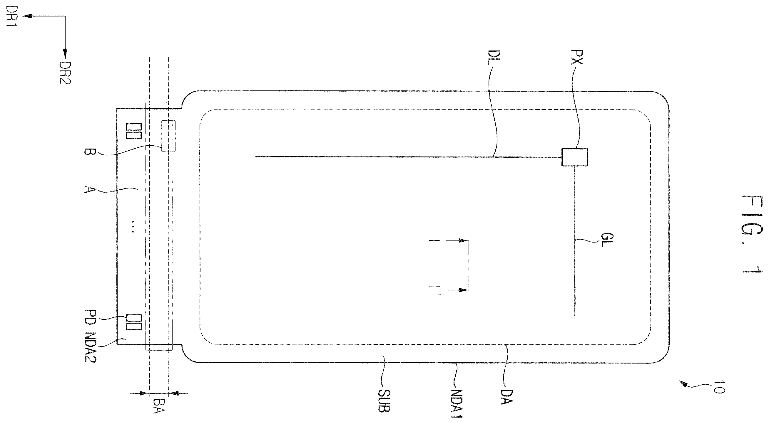
Embodiments provide a display device with improved reliability. A display device according to an embodiment includes: a substrate including a display area, a first non-display area adjacent to the display area, a second non-display area spaced apart from the first non-display area in a first direction, and a bending area disposed between the first non-display area and the second non-display area and extending in a second direction crossing the first direction, a first inorganic film disposed in the display area, the first non-display area, the second non-display area and a portion of the bending area on the substrate, a second inorganic film disposed on the first inorganic film and overlapping the display area, the first non-display area, and the second non-display area in a plan view, a first power line disposed on the second inorganic film and overlapping the first non-display area in a plan view, and a first dummy line extending from the first power line, disposed on the first inorganic film in the bending area, covering a first side surface of the second inorganic film in the first non-display area, and extending in the second direction. In an embodiment, the first dummy line may be monolithic with the first power line. In an embodiment, the first dummy line may extend along the bending area in the second direction, and a length of the first dummy line in the second direction may be the same as a length of the bending area in the second direction. In an embodiment, the second inorganic film may expose the first inorganic film in the bending area, and the first inorganic film may expose the substrate in the bending area. In an embodiment, a length of a portion of the first dummy line overlapping the bending area in the first direction may be less than a length of a portion of the first inorganic film overlapping the bending area in the first direction. In an embodiment, the display device may further include a second power line disposed in the first non-display area on the second inorganic film and spaced apart from the first power line in the plan view. In an embodiment, the second power line may be disposed in the same layer as the first power line, and the second power line may be spaced apart from the first dummy line in the plan view. In an embodiment, the second power line may overlap the first dummy line in the first direction. In an embodiment, the display device may further include an organic film disposed on the first power line and overlapping the display area, the first non-display area, the second non-display area, and the bending area. In an embodiment, the organic film may cover the first dummy line, the first inorganic film and the second inorganic film. In an embodiment, the display device may further include a third power line disposed on the second inorganic film, overlapping the second non-display area, disposed on the same layer as the first power line, and spaced apart from the first power line in the first direction in the plan view. In an embodiment, the display device may further include a second dummy line extending from the third power line, disposed on the first inorganic film in the bending area, covering a second side surface of the second inorganic film spaced apart from the first side surface in the second non-display area, and extending in the second direction. In an embodiment, the second dummy line may be spaced apart from the first dummy line in the first direction. In an embodiment, the second dummy line may extend along the bending area in the second direction, and a length of the second dummy line in the second direction may be the same as a length of the first dummy line in the second direction. A display device according to an embodiment includes: a substrate including a display area, a first non-display area adjacent to the display area, a second non-display area spaced apart from the first non-display area in a first direction, and a bending area disposed between the first non-display area and the second non-display area and extending in a second direction crossing the first direction, a first inorganic film disposed in the display area, the first non-display area, the second non-display area, and a portion of the bending area on the substrate and defining a first opening extending in the second direction in the bending area, a second inorganic film in the display area, the first non-display area, and the second non-display area on the first inorganic film and defining a second opening extending in the second direction in the bending area, a first power line disposed in the first non-display area on the second inorganic film and a first dummy line extending from the first power line, disposed on the first inorganic film in the bending area, covering a first side surface of the second opening in the first non-display area, and extending in the second direction. In an embodiment, the first opening and the second opening may overlap each other in the bending area in a plan view. In an embodiment, the first dummy line may be spaced apart from the first opening. In an embodiment, the display device may further include a second power line disposed in the same layer as the first power line and spaced apart from the first power line, a third power line disposed in the same layer as the first power line and spaced apart from the first power line and the second power line and a second dummy line extending from the third power line, disposed on the first inorganic film in the bending area, covering a second side surface of the second opening in the second non-display area, and extending in the second direction. In an embodiment, the second dummy line is spaced apart from the first opening, the second dummy line may be spaced apart from the first dummy line, and the first opening may be interposed between the first dummy line and the second dummy line. In an embodiment, the display device may further include an organic film disposed on the first power line and overlapping the display area, the first non-display area, the second non-display area, and the bending area, and the organic film may be disposed in the first opening and the second opening and contacts the substrate in the bending area. In the display device according to embodiments, as the first dummy line is disposed in a boundary between the first non-display area and the bending area, and the second dummy line is disposed in a boundary between the bending area and the second non-display area, the residual metal film may not remain in the boundary between the first non-display area and the bending area and the boundary between the second non-display area and the bending area. Accordingly, a short circuit due to the residual metal film may be prevented, and thus, the reliability of the display device may be effectively improved.
BRIEF DESCRIPTION OF THE DRAWINGS
is a plan view illustrating a display device according to an embodiment. is a cross-sectional view taken along line I-I′ of . is a plan view illustrating an enlarged area A of . is a cross-sectional view taken along line II-IF of . is a cross-sectional view taken along line of . is a plan view illustrating an enlarged area B of . is a plan view illustrating an enlarged area C of . is a cross-sectional view taken along line IV-IV′ of . is a cross-sectional view taken along line V-V′ of . is a cross-sectional view illustrating another example of . is a cross-sectional view illustrating another example of . to 19 are views for explaining a method of manufacturing a display device according to embodiments.
DETAILED DESCRIPTION
It will be understood that when an element is referred to as being “on” another element, it can be directly on the other element or intervening elements may be present therebetween. In contrast, when an element is referred to as being “directly on” another element, there are no intervening elements present. It will be understood that, although the terms “first,” “second,” “third” etc. may be used herein to describe various elements, components, regions, layers and/or sections, these elements, components, regions, layers and/or sections should not be limited by these terms. These terms are only used to distinguish one element, component, region, layer or section from another element, component, region, layer or section. Thus, “a first element,” “component,” “region,” “layer” or “section” discussed below could be termed a second element, component, region, layer or section without departing from the teachings herein. The terminology used herein is for the purpose of describing particular embodiments only and is not intended to be limiting. As used herein, “a”, “an,” “the,” and “at least one” do not denote a limitation of quantity, and are intended to include both the singular and plural, unless the context clearly indicates otherwise. For example, “an element” has the same meaning as “at least one element,” unless the context clearly indicates otherwise. “At least one” is not to be construed as limiting “a” or “an.” “Or” means “and/or.” As used herein, the term “and/or” includes any and all combinations of one or more of the associated listed items. It will be further understood that the terms “comprises” and/or “comprising,” or “includes” and/or “including” when used in this specification, specify the presence of stated features, regions, integers, steps, operations, elements, and/or components, but do not preclude the presence or addition of one or more other features, regions, integers, steps, operations, elements, components, and/or groups thereof. Hereinafter, display devices in accordance with embodiments will be described in more detail with reference to the accompanying drawings. The same reference numerals are used for the same components in the drawings, and redundant descriptions of the same components will be omitted. is a plan view illustrating a display device according to an embodiment. As used herein, the “plan view” is a view from a third direction DR 3 , and the third direction DR 3 is a thickness direction of the display device, and perpendicular to the first direction DR 1 and the second direction DR 2 . Referring to , a display device 10 may include a substrate SUB. The substrate SUB may include a display area DA, a first non-display area NDA 1 , a second non-display area NDA 2 , and a bending area BA. The display area DA may display a screen. A plurality of pixels PX which emit light and lines which transmit a driving signal to the pixels PX may be disposed in the display area DA. Examples of the lines may include gate lines GL and data lines DL. The gate lines GL may transmit a gate signal, and the data lines DL may transmit a data signal. The first non-display area NDA 1 may be an area which does not display a screen. The lines and drivers for driving may be disposed in the first non-display area NDA 1 . For example, a gate driver and a light emitting driver may be disposed in the first non-display area NDA 1 . The first non-display area NDA 1 may be adjacent to the display area DA and may surround at least one surface of the display area DA. However, embodiments according to the invention are not limited thereto, and the screen may be displayed in the first non-display area NDA 1 in another embodiment. The second non-display area NDA 2 may be spaced apart from the first non-display area NDA 1 in a first direction DR 1 . Similarly, the second non-display area NDA 2 may be an area which does not display a screen. The lines and the drivers for driving may be disposed in the second non-display area NDA 2 . For example, a pad unit PD including pads and a driving chip may be disposed in the second non-display area NDA 2 . However, embodiments according to the invention are not limited thereto, and the pad unit PD and a circuit board on which the driving chip is mounted may be connected in the second non-display area NDA 2 in another embodiment. The bending area BA may be disposed between the first non-display area NDA 1 and the second non-display area NDA 2 . The bending area BA may extend in a second direction DR 2 crossing the first direction DR 1 . The bending area BA may be bent to reduce an area of the non-display areas. Accordingly, as the bending area BA is bent, the second non-display area NDA 2 may be positioned on a rear surface of the display device 10 , so that an area of the non-display area of the display device 10 may be reduced. is a cross-sectional view taken along line I-I′ of . Referring to , the display device 10 may include the substrate SUB, a barrier layer BRR, a buffer layer BFR, a first active pattern ACT 1 , a second active pattern ACT 2 , and a first insulation layer IL 1 , a first gate electrode GAT 1 , a first gate line GWL, a second insulation layer IL 2 , a second gate electrode GAT 2 , a third insulation layer IL 3 , a third active pattern ACT 3 , a fourth insulation layer IL 4 , a second gate line GCL, a fifth insulation layer IL 5 , a first connection pattern CP 1 , a second connection pattern CP 2 , a third connection pattern CP 3 , a fourth connection pattern CP 4 , a sixth insulation layer IL 6 , a data line DL, a seventh insulation layer IL 7 , an anode electrode ADE, a pixel defining layer PDL, and a light emitting layer EL, and a cathode electrode CTE. The substrate SUB may be formed of glass, quartz, plastic, or the like. Examples of the material which may be used as the plastic include polyimide (“PI”), polyacrylate, polymethylmethacrylate (“PMMA”), polycarbonate (“PC”), polyethylenenaphthalate (“PEN”), polyvinylidene chloride, polyvinylidene difluoride (“PVDF”), polystyrene, ethylene vinylalcohol copolymer, polyethersulphone (“PES”), polyetherimide (“PEI”), polyphenylene sulfide (“PPS”), polyallylate, tri-acetyl cellulose (“TAC”), cellulose acetate propionate (“CAP”), etc. These materials may be used alone or in combination. The barrier layer BRR may be disposed on the substrate SUB. The barrier layer BRR may prevent foreign substances from penetrating under the substrate SUB. The barrier layer BRR may be formed of an inorganic material. Examples of the inorganic material may include silicon oxide, silicon nitride, silicon oxynitride, etc. These materials may be used alone or in combination. The buffer layer BFR may be disposed on the barrier layer BRR. In an embodiment, the buffer layer BFR may be formed of an inorganic material. Examples of the inorganic material may include silicon oxide, silicon nitride, silicon oxynitride, etc. These materials may be used alone or in combination. The buffer layer BFR may prevent metal atoms or impurities from penetrating into the first and second active patterns ACT 1 and ACT 2 . In addition, the buffer layer BFR may control a heat supply rate during a crystallization process to form the first and second active patterns ACT 1 and ACT 2 . The first to third active patterns ACT 1 , ACT 2 , and ACT 3 may be disposed on the buffer layer BFR. In an embodiment, the first to third active patterns ACT 1 , ACT 2 , and ACT 3 may be formed of a silicon semiconductor material. Examples of the silicon semiconductor material may include amorphous silicon and polycrystalline silicon. These materials may be used alone or in combination. The first insulation layer IL 1 may be disposed on the buffer layer BFR and may cover the first to third active patterns ACT 1 , ACT 2 , and ACT 3 . In an embodiment, the first insulation layer IL 1 may be formed of an inorganic material. Examples of the inorganic material include silicon oxide, silicon nitride, silicon oxynitride, etc. These materials may be used alone or in combination. The first gate electrode GAT 1 , the first gate line GWL, and the second gate line GCL may be disposed on the first insulation layer IL 1 . In an embodiment, the first gate electrode GAT 1 may overlap the first active pattern ACT 1 in a plan view. The first active pattern ACT 1 and the first gate electrode GAT 1 may constitute a first transistor T 1 . In an embodiment, the first gate line GWL may overlap the second active pattern ACT 2 . The second active pattern ACT 2 and the first gate line GWL may constitute a second transistor T 2 . In an embodiment, the second gate line GCL may overlap the third active pattern ACT 3 . The third active pattern ACT 3 and the second gate line GCL may constitute a third transistor T 3 . In an embodiment, the first gate electrode GAT 1 , the first gate line GWL, and the second gate line GCL may be formed of a metal, an alloy, a conductive metal oxide, a transparent conductive material, or the like. Examples of materials which can be used as the first gate electrode GAT 1 , the first gate line GWL, and the second gate line GCL may include silver (Ag), an alloy containing silver, molybdenum (Mo), alloys containing molybdenum, aluminum (Al), alloys containing aluminum, aluminum nitride (AlN), tungsten (W), tungsten nitride (WN), copper (Cu), nickel (Ni), chromium (Cr), chromium nitride (CrN), titanium (Ti), tantalum (Ta), platinum (Pt), scandium (Sc), indium tin oxide (“ITO”), indium zinc oxide (“IZO”), or the like. These materials may be used alone or in combination. The second insulation layer IL 2 may be disposed on the first insulation layer IL 1 and may cover the first gate electrode GAT 1 , the first gate line GWL, and the second gate line GCL. In an embodiment, the second insulation layer IL 2 may be formed of an inorganic material. The second gate electrode GAT 2 may be disposed on the second insulation layer IL 2 . In an embodiment, the second gate electrode GAT 2 may overlap the first gate electrode GAT 1 in a plan view. The first gate electrode GAT 1 and the second gate electrode GAT 2 may constitute a storage capacitor. In an embodiment, the second gate electrode GAT 2 may be formed of a metal, an alloy, a conductive metal oxide, a transparent conductive material, or the like. The third insulation layer IL 3 may be disposed on the second insulation layer IL 2 and cover the second gate electrode GAT 2 . In an embodiment, the third insulation layer IL 3 may be formed of an inorganic material. The first connection pattern CP 1 and the second connection pattern CP 2 may be disposed on the third insulation layer IL 3 . The first and second connection patterns CP 1 and CP 2 may contact the third active pattern ACT 3 . The first and second connection patterns CP 1 and CP 2 may be formed of a metal, an alloy, a conductive metal oxide, a transparent conductive material, or the like. The fourth insulation layer IL 4 may be disposed on the third insulation layer IL 3 . The fourth insulation layer IL 4 may cover and protect the first and second connection patterns CP 1 and CP 2 . In an embodiment, the fourth insulation layer IL 4 may be formed of an insulating material. The fifth insulation layer IL 5 may be disposed on the fourth insulation layer IL 4 . In an embodiment, the fifth insulation layer IL 5 may be formed of an organic material. The third and fourth connection patterns CP 3 and CP 4 may be disposed on the fifth insulation layer IL 5 . The third and fourth connection patterns CP 3 and CP 4 may contact the third active pattern ACT 3 . In an embodiment, the third and fourth connection patterns CP 1 , CP 2 , CP 3 , and CP 4 may be formed of a metal, an alloy, a conductive metal oxide, a transparent conductive material, or the like. The sixth insulation layer IL 6 may be disposed on the fifth insulation layer IL 5 and may cover the third and fourth connection patterns CP 3 and CP 4 . In an embodiment, the sixth insulation layer IL 6 may be formed of an organic material. Examples of the organic material may include photoresists, polyacrylic resins, polyimide resins, acrylic resins, and the like. These materials may be used alone or in combination. Accordingly, the sixth insulation layer IL 6 may have a substantially flat top surface. The data line DL may be disposed on the sixth insulation layer IL 6 . In an embodiment, the data line DL may contact the third connection pattern CP 3 . A data signal may be provided to the data line DL. In an embodiment, the data line DL may be formed of a metal, an alloy, a conductive metal oxide, a transparent conductive material, or the like. The seventh insulation layer IL 7 may be disposed on the sixth insulation layer IL 6 and may cover the data line DL. In an embodiment, the seventh insulation layer IL 7 may be formed of an organic material. The anode electrode ADE may be disposed on the seventh insulation layer IL 7 . In an embodiment, the anode electrode ADE may be formed of a metal, an alloy, a conductive metal oxide, a transparent conductive material, or the like. The pixel defining layer PDL may be disposed on the seventh insulation layer IL 7 . An opening exposing the anode electrode ADE may be formed in the pixel defining layer PDL. In an embodiment, the pixel defining layer PDL may be formed of an organic material. The light emitting layer EL may be disposed on the anode electrode ADE. The light emitting layer EL may include an organic material emitting light. In an embodiment, the light emitted from the light emitting layer EL may be emitted toward the cathode electrode CTE. The cathode electrode CTE may be disposed on the light emitting layer EL. The cathode electrode CTE may receive a power supply voltage. The light emitting layer EL may emit light based on a voltage difference between the anode electrode ADE and the cathode electrode CTE. is a plan view illustrating an enlarged area A of . is a cross-sectional view taken along line II-IF of . is a cross-sectional view taken along line of . In an embodiment, for example, may be a plan view illustrating only a first power line PL 1 and a first dummy line DML 1 . Referring to to 5 , the display device 10 may further include a first power line PL 1 , a second power line (e.g., refer to the second power line PL 2 of ), and a third power line PL 3 , a first dummy line DML 1 , a second dummy line DML 2 , first lines (e.g., first lines LN 1 of ), second lines (e.g., second lines LN 2 of ) and third lines. The barrier layer BRR, the buffer layer BFR, the first insulation layer IL 1 , the second insulation layer IL 2 , the third insulation layer IL 3 , the fourth insulation layer IL 4 , the fifth insulation layer IL 5 , the sixth insulation layer IL 6 , the seventh insulation layer IL 7 , and the pixel defining layer PDL may be disposed to extend from the display area to the first non-display area NDA 1 . In an embodiment, the barrier layer BRR and the buffer layer BFR may form a first inorganic film IF 1 . The first insulation layer IL 1 , the second insulation layer IL 2 , and the third insulation layer IL 3 may form a second inorganic film IF 2 . The fifth insulation layer IL 5 , the sixth insulation layer IL 6 , and the seventh insulation layer IL 7 may form an organic film OF. However, embodiments according to the invention are not limited thereto. Hereinafter, the first inorganic film IF 1 , the second inorganic film IF 2 , and the organic film OF may be described as a reference. In an embodiment, the bending area BA may include a first bending area BA 1 adjacent to the first non-display area NDA 1 , a second bending area BA 2 adjacent to the second non-display area NDA 2 , and a third bending area BA 3 disposed between the first bending area BA 1 and the second bending area BA 2 . The first inorganic film IF 1 may be disposed on the substrate SUB. The first inorganic film IF 1 may be entirely disposed in the display area DA, the first non-display area NDA 1 , and the second non-display area NDA 2 . The first inorganic film IF 1 may be disposed on a portion of the bending area BA. For example, the first inorganic film IF 1 may be disposed to overlap the first bending area BA 1 and the second bending area BA 2 . The first inorganic film IF 1 may not overlap the third bending area BA 3 in a plan view. Accordingly, in the third bending area BA 3 , the first inorganic film IF 1 may expose the substrate SUB. In an embodiment, the first inorganic film IF 1 may define a first opening OP 1 extending in the second direction DR 2 in the bending area BA. The second inorganic film IF 2 may be disposed on the first inorganic film IF 1 . The second inorganic film IF 2 may overlap the display area DA, the first non-display area NDA 1 , and the second non-display area NDA 2 . The second inorganic film IF 2 may not overlap the bending area BA in a plan view. Accordingly, the second inorganic film IF 2 may expose the first inorganic film IF 1 in the bending area BA. For example, the second inorganic film IF 2 may expose the first inorganic film IF 1 in the first bending area BA 1 and the second bending area BA 2 . In an embodiment, the second inorganic film IF 2 may define a second opening OP 2 extending in the second direction DR 2 in the bending area BA. The second opening OP 2 may overlap the first opening OP 1 in a plan view. A length of the first opening OP 1 in the first direction DR 1 may be less than a length of the second opening OP 2 in the first direction DR 1 . Accordingly, an area of the first opening OP 1 may be less than an area of the second opening OP 2 . Accordingly, the bending area BA may be defined as an area in which the second inorganic film IF 2 is not disposed. Also, the third bending area BA 3 may be defined as an area in which the first inorganic film IF 1 is not disposed. However, embodiments according to the invention are not limited thereto. The first power line PL 1 may transmit a first power voltage to the pixels PX. The first power line PL 1 may be connected to the third power line PL 3 through the first lines (e.g., the first lines LN 1 of ). That is, the first power line PL 1 and the third power line PL 3 may be connected through the first lines. However, embodiments according to the invention are not limited thereto, and the first lines may be connected to the pad unit PD in another embodiment. The first power line PL 1 may be disposed on the second inorganic film IF 2 . The first power line PL 1 may overlap the first non-display area NDA 1 in a plan view. The first power line PL 1 may be disposed on the same layer as the first conductive pattern CP 1 and the second conductive pattern CP 2 in the display area DA. In an embodiment, the first dummy line DML 1 may extend from the first power line PL 1 . That is, the first dummy line DML 1 may be integrally formed (i.e., monolithic) with the first power line PL 1 . For example, the first dummy line DML 1 may be connected to the first power line PL 1 in six portions. However, embodiments according to the invention are not limited thereto. The first dummy line DML 1 may extend in the second direction DR 2 along the bending area BA in another embodiment. A length L 1 of the first dummy line DML 1 in the second direction DR 2 may be substantially the same as a length L 2 of the bending area BA in the second direction DR 2 . Accordingly, the first dummy line DML 1 may cover the entirety of a boundary between the first non-display area NDA 1 and the bending area BA. However, embodiments according to the invention are not limited thereto, and the length L 1 of the first dummy line DML may be smaller than the length L 2 of the bending area BA in another embodiment. The first dummy line DML 1 may be disposed on the first inorganic film IF 1 in the bending area BA. The first dummy line DML 1 may cover a first side surface IF 2 a of the second inorganic film IF 2 in the first non-display area NDA 1 . A length L 3 of a portion of the first dummy line DML 1 overlapping with the bending area BA in the first direction DR 1 may less than a length L 4 of a portion of the first inorganic film IF 1 overlapping the bending area BA in the first direction DR 1 . That is, the first dummy line DML 1 may only partially overlap the first inorganic film IF 1 . Accordingly, the first dummy line DML 1 may expose the first inorganic film IF 1 in the first bending area BA 1 . The first dummy line DML 1 may cover a side surface of the second opening OP 2 in the first non-display area NDA 1 . The side surface of the second opening OP 2 may be substantially the same as the first side surface IF 2 a of the second inorganic film IF 2 . Also, the first dummy line DML 1 may be spaced apart from the first opening OP 1 . The third power line PL 3 may transfer the first power voltage to the pixels PX. The third power line PL 3 may be connected to the pad unit PD through the third lines. The third power line PL 3 may be disposed on the second inorganic film IF 2 . The third power line PL 3 may overlap the second non-display area NDA 2 in a plan view. The third power line PL 3 may be disposed on the same layer as the first power line PL 1 . The third power line PL 3 may be spaced apart from the first power line PL 1 in a plan view. For example, the third power line PL 3 may be spaced apart from the first power line PL 1 in the first direction DR 1 . The second dummy line DML 2 may be spaced apart from the first dummy line DML 1 in the first direction DR 1 . The second dummy line DML 2 may extend from the third power line PL 3 . For example, the second dummy line DML 2 may be connected to the third power line PL 3 in six portions. However, embodiments according to the invention are not limited thereto. The second dummy line DML 2 may be disposed on the first inorganic film IF 1 in the bending area BA. The second dummy line DML 2 may cover a second side surface IF 2 b of the second inorganic film IF 2 in the second non-display area NDA 2 . The second side surface IF 2 b of the second inorganic film IF 2 may be spaced apart from the first side surface IF 2 a of the second inorganic film IF 2 and may overlap the second non-display area NDA 2 in a plan view. The second dummy line DML 2 may extend along the bending area BA in the second direction DR 2 like the first dummy line DML 1 . A length L 5 of the second dummy line DML 2 in the second direction DR 2 may be substantially the same as a length L 1 of the first dummy line DML 1 in the second direction DR 2 . For example, a shape of the second dummy line DML 2 may be substantially symmetrical to a shape of the first dummy line DML 1 . However, the shape of the second dummy line DML 2 is not limited thereto. The organic film OF may be disposed on the first power line PL 1 and the second power line PL 2 . The organic film OF may overlap the entirety of the display area DA, the first non-display area NDA 1 , the second non-display area NDA 2 , and the bending area BA. In addition, the organic film OF may cover the entirety of the first dummy line DML 1 , the second dummy line DML 2 , the first inorganic film IF 1 , and the second inorganic film IF 2 . In an embodiment, the organic film OF may be disposed in the first opening OP 1 and the second opening OP 2 . The organic film OF may be disposed on the second inorganic film IF 2 in the first non-display area NDA 1 and overlap the first inorganic film IF 1 in the first bending area BA 1 in a plan view. The organic film OF may contact the substrate SUB in the third bending area BA 3 . In an embodiment, as the first dummy line DML 1 is disposed in a boundary between the first non-display area NDA 1 and the bending area BA, and the second dummy line DML 2 is disposed in the boundary between the bending area BA and the second non-display area NDA 2 , the boundary between the first non-display area NDA 1 and the bending area BA and the boundary between the second non-display area NDA 2 and the bending area BA may not remain residual metal film. Accordingly, a short circuit caused by the residual metal film may be prevented, and thus, a reliability of the display device 10 may be improved. is a plan view illustrating an enlarged area B of . is a plan view illustrating an enlarged area C of . Referring to , the first power line PL 1 , the second power line PL 2 , and the third power line PL 3 may be disposed on the second inorganic film IF 2 . The second power line PL 2 may be disposed on the same layer as the first power line PL 1 . The second power line PL 2 may be spaced apart from the first power line PL 1 in a plan view. Also, the second power line PL 2 may be spaced apart from the first dummy line DML 1 in the plan view. The second power line PL 2 may overlap the first dummy line DML 1 in the first direction DR 1 . The second power line PL 2 may transmit a second power voltage different from the first power voltage to the pixels PX. The second power line PL 2 may be connected to the pad unit PD through the second lines LN 2 . The display device 10 may further include fan-out lines FOL and connection lines CL. The fan-out lines FOL may be spaced apart from the first lines LN 1 in the second direction DR 2 . The fan-out lines FOL may extend in the first direction DR 1 and may be connected to the connection lines CL. The fan-out lines FOL may be connected to the driving chip. Optionally, the fan-out lines FOL may be connected to the pad unit PD connected to the driving chip. The fan-out lines FOL may receive the data signal from the driving chip and transmit the data signal to the connection lines CL. The connection lines CL may be connected to the data lines DL disposed in the display area DA, respectively, and may transmit the data signal to the data lines DL. The connection lines CL may include first connection lines CL 1 and second connection lines CL 2 . The first connection lines CL 1 and the second connection lines CL 2 may be disposed on different layers. The first connection lines CL 1 and the second connection lines CL 2 may extend parallel to each other and may be alternately disposed. is a cross-sectional view taken along line of . is a cross-sectional view taken along line v-v′ of . Referring further to , the first lines LN 1 may be disposed on the fifth insulation layer IL 5 . The first lines LN 1 may be disposed on the same layer as the third conductive pattern CP 3 and the fourth conductive pattern CP 4 in the display area DA. The sixth insulation layer IL 6 may cover the first lines LN 1 . The first lines LN 1 may be connected to the first power line PL 1 through at least one contact hole. The first lines LN 1 may be connected to the third power line PL 3 . However, embodiments according to the invention are not limited thereto, and the first lines LN 1 may be connected to the pad unit PD in another embodiment. Referring further to , the fan-out lines FOL may be disposed on the same layer as the first lines LN 1 . For example, the fan-out lines FOL may be disposed on the fifth insulation layer IL 5 . The sixth insulation layer IL 6 may cover the fan-out lines FOL. The fan-out lines FOL may be connected to the connection lines CL, respectively. The fan-out lines FOL may be connected to the first connection lines CL 1 and the second connection lines CL 2 through contact holes, respectively. The first connection lines CL 1 and the second connection lines CL 2 may be disposed on different layers. For example, the first connection lines CL 1 may be disposed on the first insulation layer IL 1 . The second connection lines CL 2 may be disposed on the second insulation layer IL 2 . For example, the first connection lines CL 1 may be disposed on the same layer as the first gate line GWL, the second gate line GCL, and the first gate electrode GAT 1 in the display area DA. The second connection lines CL 2 may be disposed on the same layer as the second gate electrode GAT 2 . However, embodiments according to the invention are not limited thereto. is a cross-sectional view illustrating another example of . is a cross-sectional view illustrating another example of . In the embodiments described with reference to , description overlapping with the embodiments described with reference to may be omitted. Referring to , first lines LN 1 may be disposed on the sixth insulation layer IL 6 . The seventh insulation layer IL 7 may cover the first lines LN 1 . Each of the first lines LN 1 may be connected to the first power line PL 1 through first patterns PT 1 . For example, the first lines LN 1 may contact each of the first patterns PT 1 through a contact hole penetrating the sixth insulation layer IL 6 . The first patterns PT 1 may contact the first power line PL 1 through a contact hole penetrating the fifth insulation layer IL 5 and the fourth insulation layer IL 4 . The fan-out lines FOL may be disposed on the same layer as the first lines LN 1 . The fan-out lines FOL may be disposed on the sixth insulation layer IL 6 . The seventh insulation layer IL 7 may cover the fan-out lines FOL. In an embodiment, for example, the first lines LN 1 and the fan-out lines FOL may be disposed on the same layer as the data line DL in the display area DA. The fan-out lines FOL may be connected to the connection lines CL, respectively. For example, the fan-out lines FOL may be connected to the second patterns PT 2 through contact holes penetrating the sixth insulation layer IL 6 . The second patterns PT 2 may be connected to the second connection lines CL 2 through contact holes passing through the fifth insulation layer IL 5 , the fourth insulation layer IL 4 , and the third insulation layer IL 3 , respectively. However, embodiments according to the invention are not limited thereto, and the fan-out lines FOL and the first lines LN 1 may be disposed on different layers. in another embodiment to 19 are views for explaining a method of manufacturing a display device according to embodiments. is a cross-sectional view taken along line VI-VI′ of , is a cross-sectional view taken along line VII-VII′ of . is a cross-sectional view taken along line VIII-VIII′ of and is a cross-sectional view taken along line IX-IX′ of . A method of manufacturing the display device described with reference to to 19 may be the method of manufacturing the display device 10 described with reference to to 11 . Accordingly, overlapping descriptions may be omitted. Referring to , a substrate SUB may be prepared. The substrate SUB may include a display area DA, a first non-display area NDA 1 , a second non-display area NDA 2 , and a bending area BA. The bending area BA may include a first bending area BA 1 , a second bending area BA 2 , and a third bending area BA 3 . A barrier layer BRR and a buffer layer BFR may be sequentially formed on the entire substrate SUB. The barrier layer BRR and the buffer layer BFR may form a first inorganic film IF 1 . A first insulation layer ILL a second insulation layer IL 2 , and a third insulation layer IL 3 may be sequentially formed on the first inorganic film IF 1 . The first insulation layer ILL the second insulation layer IL 2 , and the third insulation layer IL 3 may form a second inorganic film IF 2 . A portion of the second inorganic film IF 2 which overlaps with the bending area BA may be removed. Accordingly, a second opening OP 2 overlapping the bending area BA may be formed in the second inorganic film IF 2 . Referring to , a conductive layer CDL may be formed on the second inorganic film IF 2 . The conductive layer CDL may be entirely formed on the second inorganic film IF 2 , and may overlap the display area DA, the first non-display area NDA 1 , the second non-display area NDA 2 , and the bending area BA. The conductive layer CDL may include a metal. Referring to , the conductive layer CDL may form a first power line PL 1 , a second power line PL 2 , a third power line, a first dummy line DML 1 , and a second dummy line through a patterning process. The first power line PL 1 , the second power line PL 2 , and the third power line may be formed to be spaced apart from each other. The first dummy line DML 1 may be integrally formed (i.e., monolithic) with the first power line PL 1 . The second dummy line may be integrally formed with the third power line. The first dummy line DML 1 and the second dummy line (e.g., the second dummy line DML 2 of ) may be formed to be spaced apart from each other in the first direction DR 1 . The first dummy line DML 1 may cover the first side surface IF 2 a of the second inorganic film IF 2 . That is, the first dummy line DML 1 may be formed in a boundary between the first non-display area NDA 1 and the bending area BA. The second dummy line may cover a second side surface (e.g., the second side surface IF 2 b of ) spaced apart from the first side surface IF 2 a of the second inorganic film IF 2 in the first direction DR 1 and may be formed in a boundary between the second non-display area NDA 2 and the bending area BA (refer to ). Each of the first dummy line DML 1 and the second dummy line may be formed to extend in the second direction DR 2 . After the conductive layer CDL is patterned, a portion of the first inorganic film IF 1 which overlaps the third bending area BA 3 included in the bending area BA may be removed. Accordingly, a first opening OP 1 overlapping the third bending area BA 3 may be formed in the first inorganic film IF 1 . Referring to , a fourth insulation layer IL 4 , a fifth insulation layer IL 5 , a sixth insulation layer IL 6 , and a seventh insulation layer IL 7 may be sequentially formed to cover the first power line PL 1 , the second power line PL 2 , the third power line, the first dummy line DML 1 , and the second dummy line. The fifth insulation layer IL 5 , the sixth insulation layer IL 6 , and the seventh insulation layer IL 7 may form an organic film OF. In addition, first lines LN 1 , second lines, and fan-out lines FOL may be formed on the fifth insulation layer IL 5 or the sixth insulation layer IL 6 . The first lines LN 1 may be connected to the first power line PL 1 through a contact hole or patterns (e.g., the first patterns PT 1 of ). The fan-out lines FOL may connect connection lines (e.g., the connection lines CL 1 and CL 2 of , 9 , and 11 ) through contact holes or patterns (e.g., the second patterns PT 2 of ). The organic film OF may overlap the entirety of the display area DA, the first non-display area NDA 1 , the second non-display area NDA 2 , and the bending area BA, and may be formed in the first opening OP 1 and the second opening OP 2 . In an embodiment, as the first dummy line DML 1 is formed in the boundary between the first non-display area NDA 1 and the bending area BA and the second dummy line is formed in the boundary between the bending area BA and the second non-display area NDA 2 , it is possible to prevent residual metal film from remaining in the patterning process of the conductive layer CDL. Accordingly, a short circuit caused by the residual metal film may be prevented, and thus, the reliability of the display device may be improved. The display device according to the embodiments may be applied to a display device included in a computer, a notebook, a mobile phone, a smartphone, a smart pad, a PMP, a PDA, an MP3 player, or the like. Although the display device according to the embodiments have been described with reference to the drawings, the illustrated embodiments are examples, and may be modified and changed by a person having ordinary knowledge in the relevant technical field without departing from the technical spirit described in the following claims.
Figures (19)
Citations
This patent cites (12)
- US2019/0318690
- US2020/0089369
- US2020/0105206
- US2020/0363905
- US2021/0035496
- US2021/0183987
- US2021/0242423
- US2021/0280641
- US109065571
- US102079256
- US1020210099246
- US1020210111926