Display Device and Tiled Display Device
Abstract
A display device includes a plurality of sub-pixels, wherein a sub-pixel of the plurality of sub-pixels includes: a first pad electrode and a second pad electrode on the substrate and spaced from each other in a plan view; a light emitting device on the first pad electrode and the second pad electrode; and a first inspection transistor overlapping the first pad electrode in a thickness direction of the substrate, wherein the first inspection transistor overlaps the light emitting device in the thickness direction of the substrate.
Claims (28)
1 . A display device comprising: a plurality of sub-pixels, wherein a sub-pixel of the plurality of sub-pixels comprises: a first pad electrode and a second pad electrode on a substrate and spaced from each other in a plan view; a light emitting device on the first pad electrode and the second pad electrode; and a first inspection transistor overlapping the first pad electrode in a thickness direction of the substrate, wherein the first inspection transistor overlaps the light emitting device in the thickness direction of the substrate, wherein the sub-pixel further comprises a second inspection transistor overlapping the second pad electrode in the thickness direction of the substrate, and wherein the second inspection transistor overlaps the light emitting device in the thickness direction of the substrate.
12 . A display device comprising: a plurality of sub-pixels, wherein a sub-pixel of the plurality of sub-pixels comprises: a first pad electrode and a second pad electrode on a substrate and spaced from each other in a plan view; a light emitting device on the first pad electrode and the second pad electrode; and a first resistor unit overlapping the first pad electrode in a thickness direction of the substrate, wherein the first resistor unit overlaps the light emitting device in the thickness direction of the substrate.
19 . A display device comprising: a plurality of sub-pixels, wherein a sub-pixel of the plurality of sub-pixels comprises: a first pad electrode and a second pad electrode on a substrate and spaced from each other in a plan view; a light emitting device on the first pad electrode and the second pad electrode; and a first dummy transistor overlapping the first pad electrode in a thickness direction of the substrate, wherein the first dummy transistor overlaps the light emitting device in the thickness direction of the substrate, and wherein a gate electrode of the first dummy transistor is connected to a floating line or a gate-off voltage line configured to receive a gate-off voltage.
23 . A tiled display device comprising: a plurality of display devices; and a connection member between the plurality of display devices; wherein a first display device from among the plurality of display devices comprises a plurality of sub-pixels, wherein a sub-pixel of the plurality of sub-pixels comprises, a first pad electrode and a second pad electrode on a substrate and spaced from each other in a plan view; a light emitting device on the first pad electrode and the second pad electrode; a first thin film transistor overlapping the first pad electrode in a thickness direction of the substrate; and a second thin film transistor overlapping the second pad electrode in the thickness direction of the substrate, wherein each of the first thin film transistor and the second thin film transistor overlaps the light emitting device in the thickness direction of the substrate.
Show 24 dependent claims
2 . The display device of claim 1 , wherein a gate electrode of the first inspection transistor and a gate electrode of the second inspection transistor are connected to an inspection enable signal line.
3 . The display device of claim 1 , wherein a gate electrode of the first inspection transistor is connected to a first inspection enable signal line, and the gate electrode of the second inspection transistor is connected to a second inspection enable signal line.
4 . The display device of claim 1 , wherein a first electrode of the first inspection transistor and a first electrode of the second inspection transistor are connected to a first horizontal power supply line configured to receive a first power voltage.
5 . The display device of claim 4 , further comprising: a first data line connected to the sub-pixel and configured to receive a first data voltage; and a second data line connected to the sub-pixel and configured to receive a second data voltage; wherein the sub-pixel further comprises: a first pixel driver comprising a first transistor configured to control a control current according to the first data voltage of the first data line; a second pixel driver comprising a second transistor configured to control a driving current flowing from a first power supply line configured to receive the first power voltage to the light emitting device according to the second data voltage of the second data line; and a third pixel driver comprising a third transistor configured to adjust a period in which the driving current is applied to the light emitting device according to the control current of the first pixel driver.
6 . The display device of claim 1 , wherein a second electrode of the first inspection transistor and a second electrode of the second inspection transistor are connected to a second horizontal power supply line configured to receive a second power voltage.
7 . The display device of claim 6 , wherein a first electrode of the light emitting device is connected to the first pad electrode, a second electrode of the light emitting device is connected to the second pad electrode, and the second pad electrode is connected to a second power supply line configured to receive the second power voltage.
8 . The display device of claim 1 , wherein a first electrode of the first inspection transistor is connected to a horizontal voltage line, and a second electrode of the first inspection transistor is connected to a sense line.
9 . The display device of claim 8 , wherein the horizontal voltage line is configured to receive a predetermined voltage.
10 . The display device of claim 8 , wherein a first electrode of the second inspection transistor is connected to the horizontal voltage line, and a second electrode is connected to the sensing line.
11 . The display device of claim 10 , wherein the light emitting device is a flip chip type micro light emitting diode device.
13 . The display device of claim 12 , further comprising: a first horizontal voltage line connected to one end of the first resistor unit; and a first sensing line connected to other end of the first resistor unit.
14 . The display device of claim 13 , wherein the sub-pixel further comprises a second resistor unit overlapping the second pad electrode in the thickness direction of the substrate, and wherein the second resistor unit overlaps the light emitting device in the thickness direction of the substrate.
15 . The display device of claim 14 , further comprising: a second horizontal voltage line connected to one end of the second resistor unit; and a second sensing line connected to other end of the second resistor unit.
16 . The display device of claim 15 , wherein a same voltage is supplied to the first horizontal voltage line and the second horizontal voltage line.
17 . The display device of claim 12 , wherein the sub-pixel further comprises an inspection transistor overlapping the second pad electrode in the thickness direction of the substrate, and wherein the inspection transistor overlaps the light emitting device in the thickness direction of the substrate.
18 . The display device of claim 17 , wherein a gate electrode of the inspection transistor is connected to an inspection enable signal line, and a first electrode of the inspection transistor is connected to a horizontal voltage line, and a second electrode of the inspection transistor is connected to a sense line.
20 . The display device of claim 19 , wherein the sub-pixel further comprises a second dummy transistor overlapping the second pad electrode in the thickness direction of the substrate, and wherein the second dummy transistor overlaps the light emitting device in the thickness direction of the substrate.
21 . The display device of claim 20 , wherein a gate electrode of the second dummy transistor is connected to the floating line or the gate-off voltage line.
22 . The display device of claim 19 , wherein the light emitting device is a flip chip type micro light emitting diode device.
24 . The tiled display device of claim 23 , wherein the light emitting device is a flip chip type micro light emitting diode device.
25 . The tiled display device of claim 23 , wherein the first display device further comprises: a board; a pad on a first surface of the substrate; and a side line on the first surface of the substrate, a second surface opposite to the first surface, and one side between the first surface and the second surface, and connected to the pad.
26 . The tiled display device of claim 25 , wherein the substrate comprises glass.
27 . The tiled display device of claim 25 , wherein the first display device further comprises: a connection line on the second surface of the substrate; and a flexible film connected to the connection line through a conductive adhesive member, wherein the side line is connected to the connection line.
28 . The tiled display device of claim 25 , wherein the plurality of display devices are arranged in a matrix in M (M is a positive integer) number of rows and N (N is a positive integer) number of columns.
Full Description
Show full text →
CROSS-REFERENCE TO RELATED APPLICATION
This application claims priority to and the benefit of Korean Patent Application No. 10-2022-0013404 filed on Jan. 28, 2022 and Korean Patent Application No. 10-2022-0035150 filed on Mar. 22, 2022 in the Korean Intellectual Property Office (KIPO), the entire contents of both of which are incorporated by reference herein.
BACKGROUND
1. Field The present disclosure relates to a display device and a tiled device. 2. Description of the Related Art With the advance of information-oriented society, more and more demands are placed on display devices for displaying images in various ways. When the display device is manufactured in a large size, the defect rate of a light emitting device may increase due to an increase in the number of pixels, and productivity or reliability may decrease. To solve this problem, a tiled display device in which a large screen is realized by connecting a plurality of display devices having a relatively small size has been developed. The display device may be a flat panel display device such as a liquid crystal display, a field emitting display and a light emitting display. The light emitting display device may include an organic light emitting diode (OLED) display including an organic light emitting diode as a light emitting element or a light emitting diode display including an inorganic light emitting diode such as a light emitting diode (LED) as a light emitting element. In the case of the light emitting diode display, when an inorganic light emitting diode device is bonded to a display panel, a pad electrode may be damaged by bonding pressure.
SUMMARY
Aspects and features of embodiments of the present disclosure provide a display device capable of inspecting damage to pad electrodes. Aspects and features of embodiments of the present disclosure provide a tiled display device capable of inspecting damage to pad electrodes. However, embodiments of the present disclosure are not limited to those set forth herein. The above and other embodiments of the present disclosure will become more apparent to one of ordinary skill in the art to which the present disclosure pertains by referencing the detailed description of the present disclosure given below. According to one or more embodiments of the present disclosure, there is provided a display device including a plurality of sub-pixels. A sub-pixel of the plurality of sub-pixels includes a first pad electrode and a second pad electrode on the substrate and spaced from each other in a plan view, a light emitting device on the first pad electrode and the second pad electrode, and a first inspection transistor overlapping the first pad electrode in a thickness direction of the substrate. The first inspection transistor overlaps the light emitting device in the thickness direction of the substrate. The sub-pixel may further include a second inspection transistor overlapping the second pad electrode in the thickness direction of the substrate. The second inspection transistor may overlap the light emitting device in the thickness direction of the substrate. A gate electrode of the first inspection transistor and a gate electrode of the second inspection transistor may be connected to an inspection enable signal line. A gate electrode of the first inspection transistor may be connected to a first inspection enable signal line, and the gate electrode of the second inspection transistor may be connected to a second inspection enable signal line. A first electrode of the first inspection transistor and a first electrode of the second inspection transistor may be connected to a first horizontal power supply line configured to receive a first power voltage. The display device may further include a first data line connected to the sub-pixel and configured to receive a first data voltage, and a second data line connected to the sub-pixel and configured to receive a second data voltage. The sub-pixel may further include a first pixel driver including a first transistor configured to control a control current according to the first data voltage of the first data line, a second pixel driver including a second transistor configured to control a driving current flowing from a first power supply line configured to receive the first power voltage to the light emitting device according to the second data voltage of the second data line, and a third pixel driver including a third transistor configured to adjust a period in which the driving current is applied to the light emitting device according to the control current of the first pixel driver. A second electrode of the first inspection transistor and a second electrode of the second inspection transistor may be connected to a second horizontal power supply line configured to receive a second power voltage. A first electrode of the light emitting device may be connected to the first pad electrode, a second electrode of the light emitting device may be connected to the second pad electrode, and the second pad electrode may be connected to a second power supply line configured to receive the second power voltage. A first electrode of the first inspection transistor may be connected to a horizontal voltage line, and a second electrode of the first inspection transistor may be connected to a sense line. The horizontal voltage line is configured to receive a predetermined voltage. A first electrode of the second inspection transistor may be connected to the horizontal voltage line, and a second electrode may be connected to the sensing line. The light emitting device may be a flip chip type micro light emitting diode device. According to one or more embodiments of the present disclosure, there is provided a display device including a plurality of sub-pixels. A sub-pixel of the plurality of sub-pixels includes a first pad electrode and a second pad electrode on the substrate and spaced from each other in a plan view; a light emitting device on the first pad electrode and the second pad electrode, and a first resistor unit overlapping the first pad electrode in a thickness direction of the substrate. The first resistor unit overlaps the light emitting device in the thickness direction of the substrate. The display device may further include a first horizontal voltage line connected to one end of the first resistor unit, and a first sensing line connected to other end of the first resistor unit. The sub-pixel may further include an inspection transistor overlapping the second pad electrode in the thickness direction of the substrate. The inspection transistor may overlap the light emitting device in the thickness direction of the substrate. A gate electrode of the inspection transistor may be connected to an inspection enable signal line, and a first electrode of the inspection transistor may be connected to a horizontal voltage line, and a second electrode of the inspection transistor is connected to a sense line. The sub-pixel may further include a second resistor unit overlapping the second pad electrode in a thickness direction of the substrate. The second resistor unit may overlap the light emitting device in a thickness direction of the substrate. The display device may further include a second horizontal voltage line connected to one end of the second resistor unit, and a second sensing line connected to other end of the second resistor unit. A same voltage may be supplied to the first horizontal voltage line and the second horizontal voltage line. According to one or more embodiments of the present disclosure, there is provided a display device including a plurality of sub-pixels. A sub-pixel of the plurality of sub-pixels includes a first pad electrode and a second pad electrode on the substrate and spaced from each other in a plan view, a light emitting device on the first pad electrode and the second pad electrode, and a first dummy transistor overlapping the first pad electrode in a thickness direction of the substrate. The first dummy transistor overlaps the light emitting device in the thickness direction of the substrate. A gate electrode of the first dummy transistor is connected to a floating line or a gate-off voltage line configured to receive a gate-off voltage. The sub-pixel may further include a second dummy transistor overlapping the second pad electrode in the thickness direction of the substrate. The second dummy transistor may overlap the light emitting device in the thickness direction of the substrate. A gate electrode of the second dummy transistor may be connected to the floating line or the gate-off voltage line. The light emitting device may be a flip chip type micro light emitting diode device. According to one or more embodiments of the present disclosure, there is provided a tiled display device including a plurality of display devices, and a connection member between the plurality of display devices. A first display device from among the plurality of display devices includes a plurality of sub-pixels. A sub-pixel of the plurality of sub-pixels includes a first pad electrode and a second pad electrode on the substrate and spaced from each other in a plan view, a light emitting device on the first pad electrode and the second pad electrode, a first thin film transistor overlapping the first pad electrode in a thickness direction of the substrate, a second thin film transistor overlapping the second pad electrode in the thickness direction of the substrate. Each of the first thin film transistor and the second thin film transistor overlaps the light emitting device in the thickness direction of the substrate. The light emitting device may be a flip chip type micro light emitting diode device. The first display device may further include a board, a pad on a first surface of the substrate, and a side line on the first surface of the substrate, a second surface opposite to the first surface, and one side between the first surface and the second surface, and connected to the pad. The substrate may include glass. The first display device may further include a connection line on the second surface of the substrate, and a flexible film connected to the connection line through a conductive adhesive member. The side line may be connected to the connection line. The plurality of display devices may be arranged in a matrix in M (M is a positive integer) number of rows and N (N is a positive integer) number of columns. According to the aforementioned and other embodiments of the present disclosure, by arranging the test transistor to overlap the light emitting device, the pad electrode that may occur when a predetermined pressure is applied to the light emitting device to attach the light emitting device to the pad electrode. It can be inspected for damage. According to the aforementioned and other embodiments of the present disclosure, it may be inspected whether the pad electrode is damaged, which may occur when a predetermined pressure is applied to the light emitting device to attach the light emitting device to the pad electrode by arranging the variable resistor to overlap the light emitting device.
BRIEF DESCRIPTION OF THE DRAWINGS
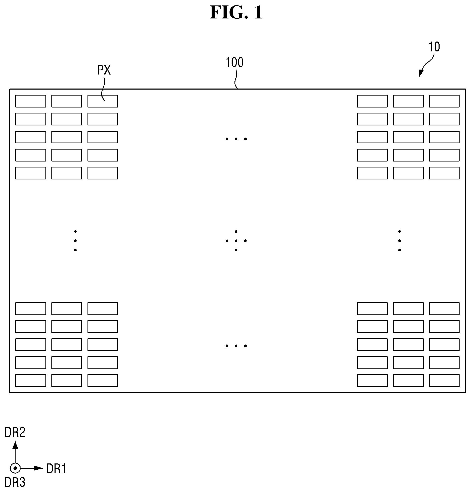
The above and other embodiments and features of the present disclosure will become more apparent by describing embodiments thereof with reference to the attached drawings, in which: is a layout diagram illustrating a display device according to one or more embodiments. is a diagram illustrating an example of the pixel of . is a diagram illustrating another example of the pixel of . is a circuit diagram illustrating a first sub-pixel according to one or more embodiments. is a layout diagram illustrating a lower metal layer, an active layer, a first gate metal layer, a second gate metal layer, a first source metal layer, and a second source metal layer of the first sub-pixel according to one or more embodiments. is a layout diagram illustrating a third source metal layer of the first sub-pixel according to one or more embodiments. is a layout diagram illustrating a fourth source metal layer of the first sub-pixel according to one or more embodiments. is a layout diagram illustrating a transparent electrode layer of the first sub-pixel and a first light emitting device according to one or more embodiments. is an enlarged layout diagram illustrating an area A of in detail. is an enlarged layout diagram illustrating an area B of . in detail. is an enlarged layout diagram illustrating an area C of in detail. is a cross-sectional view illustrating an example of the first sub-pixel taken along the line A-A′ of to 8 . is a cross-sectional view illustrating an example of the first sub-pixel taken along the line B-B′ of to 8 . is a circuit diagram illustrating the first sub-pixel according to one or more embodiments. is a circuit diagram illustrating the first sub-pixel according to one or more embodiments. is a layout diagram illustrating the lower metal layer, the active layer, the first gate metal layer, the second gate metal layer, the first source metal layer, and the second source metal layer of the first sub-pixel according to one or more embodiments. is an enlarged layout diagram illustrating an area C of in detail. is a cross-sectional view illustrating an example of the first sub-pixel taken along the line C-C′ of . is a circuit diagram illustrating the first sub-pixel according to one or more embodiments. is a layout diagram illustrating the lower metal layer, the active layer, the first gate metal layer, the second gate metal layer, the first source metal layer, and the second source metal layer of the first sub-pixel according to one or more embodiments. is an enlarged layout diagram illustrating an area C of in detail. is a cross-sectional view illustrating an example of the first sub-pixel taken along the line D-D′ of . is a circuit diagram illustrating the first sub-pixel according to one or more embodiments. is a layout diagram illustrating the lower metal layer, the active layer, the first gate metal layer, the second gate metal layer, the first source metal layer, and the second source metal layer of the first sub-pixel according to one or more embodiments. is an enlarged layout diagram illustrating an area C of in detail. is a cross-sectional view illustrating an example of the first sub-pixel taken along the line E-E′ of . is a circuit diagram illustrating the first sub-pixel according to one or more embodiments. is a layout diagram illustrating the lower metal layer, the active layer, the first gate metal layer, the second gate metal layer, the first source metal layer, and the second source metal layer of the first sub-pixel according to one or more embodiments. is an enlarged layout diagram illustrating an area C of in detail. is a cross-sectional view illustrating an example of the first sub-pixel taken along the line F-F′ of . is a circuit diagram illustrating the first sub-pixel according to one or more embodiments. is a layout diagram illustrating the lower metal layer, the active layer, the first gate metal layer, the second gate metal layer, the first source metal layer, and the second source metal layer of the first sub-pixel according to one or more embodiments. is an enlarged layout diagram showing an area C of in detail. is a cross-sectional view illustrating an example of the first sub-pixel taken along the line G-G′ of . is a circuit diagram illustrating the first sub-pixel according to one or more embodiments. is a layout diagram illustrating the lower metal layer, the active layer, the first gate metal layer, the second gate metal layer, the first source metal layer, and the second source metal layer of the first sub-pixel according to one or more embodiments. is an enlarged layout diagram illustrating a region C of in detail. is a cross-sectional view illustrating an example of the first sub-pixel taken along the line H-H′ of . is a layout diagram illustrating the lower metal layer, the active layer, the first gate metal layer, the second gate metal layer, the first source metal layer, and the second source metal layer of the first sub-pixel according to one or more embodiments. is a layout diagram illustrating the third source metal layer of the first sub-pixel according to one or more embodiments. is a layout diagram illustrating the fourth source metal layer of the first sub-pixel according to one or more embodiments. is a layout diagram illustrating the transparent electrode layer of the first sub-pixel and the first light emitting device according to one or more embodiments. is a cross-sectional view illustrating an example of the first sub-pixel taken along the line H-H′ of to 42 . is a diagram illustrating a front surface of a tiled display device according to one or more embodiments. is an enlarged layout diagram illustrating the H area of in detail. is a cross-sectional view illustrating an example of a tiled display device taken along the line J-J′ of . is a plan view illustrating a front surface of a first display device according to one or more embodiments. is a plan view illustrating a bottom of the first display device according to one or more embodiments. is a cross-sectional view illustrating an example of the first display device taken along the line N-N′ of . is a diagram illustrating an example of a test multiplexer according to one or more embodiments. is a plan view illustrating the front surface of the first display device according to one or more embodiments. is a block diagram illustrating a tiled display device according to one or more embodiments. is a diagram illustrating wireless communication between a plurality of display devices of a tiled display device according to one or more embodiments.
DETAILED DESCRIPTION
Aspects and features of embodiments of the present disclosure and methods of accomplishing the same may be understood more readily by reference to the detailed description of embodiments and the accompanying drawings. Hereinafter, embodiments will be described in more detail with reference to the accompanying drawings. The described embodiments, however, may be embodied in various different forms, and should not be construed as being limited to only the illustrated embodiments herein. Rather, these embodiments are provided as examples so that this disclosure will be thorough and complete, and will fully convey the aspects and features of the present disclosure to those skilled in the art. Accordingly, processes, elements, and techniques that are not necessary to those having ordinary skill in the art for a complete understanding of the aspects and features of the present disclosure might not be described. Unless otherwise noted, like reference numerals, characters, or combinations thereof denote like elements throughout the attached drawings and the written description, and thus, descriptions thereof will not be repeated. Further, parts not related to the description of one or more embodiments might not be shown to make the description clear. In the drawings, the relative sizes of elements, layers, and regions may be exaggerated for clarity. Additionally, the use of cross-hatching and/or shading in the accompanying drawings is generally provided to clarify boundaries between adjacent elements. As such, neither the presence nor the absence of cross-hatching or shading conveys or indicates any preference or requirement for particular materials, material properties, dimensions, proportions, commonalities between illustrated elements, and/or any other characteristic, attribute, property, etc., of the elements, unless specified. Various embodiments are described herein with reference to sectional illustrations that are schematic illustrations of embodiments and/or intermediate structures. As such, variations from the shapes of the illustrations as a result, for example, of manufacturing techniques and/or tolerances, are to be expected. Further, specific structural or functional descriptions disclosed herein are merely illustrative for the purpose of describing embodiments according to the concept of the present disclosure. Thus, embodiments disclosed herein should not be construed as limited to the particular illustrated shapes of regions, but are to include deviations in shapes that result from, for instance, manufacturing. For example, an implanted region illustrated as a rectangle will, typically, have rounded or curved features and/or a gradient of implant concentration at its edges rather than a binary change from implanted to non-implanted region. Likewise, a buried region formed by implantation may result in some implantation in the region between the buried region and the surface through which the implantation takes place. Thus, the regions illustrated in the drawings are schematic in nature and their shapes are not intended to illustrate the actual shape of a region of a device and are not intended to be limiting. Additionally, as those skilled in the art would realize, the described embodiments may be modified in various different ways, all without departing from the spirit or scope of the present disclosure. In the detailed description, for the purposes of explanation, numerous specific details are set forth to provide a thorough understanding of various embodiments. It is apparent, however, that various embodiments may be practiced without these specific details or with one or more equivalent arrangements. In other instances, well-known structures and devices are shown in block diagram form to avoid unnecessarily obscuring various embodiments. Spatially relative terms, such as “beneath,” “below,” “lower,” “under,” “above,” “upper,” and the like, may be used herein for ease of explanation to describe one element or feature's relationship to another element(s) or feature(s) as illustrated in the figures. It will be understood that the spatially relative terms are intended to encompass different orientations of the device in use or in operation, in addition to the orientation depicted in the figures. For example, if the device in the figures is turned over, elements described as “below” or “beneath” or “under” other elements or features would then be oriented “above” the other elements or features. Thus, the example terms “below” and “under” can encompass both an orientation of above and below. The device may be otherwise oriented (e.g., rotated 90 degrees or at other orientations) and the spatially relative descriptors used herein should be interpreted accordingly. Similarly, when a first part is described as being arranged “on” a second part, this indicates that the first part is arranged at an upper side or a lower side of the second part without the limitation to the upper side thereof on the basis of the gravity direction. Further, in this specification, the phrase “on a plane,” or “plan view,” means viewing a target portion from the top, and the phrase “on a cross-section” means viewing a cross-section formed by vertically cutting a target portion from the side. It will be understood that when an element, layer, region, or component is referred to as being “formed on,” “on,” “connected to,” or “coupled to” another element, layer, region, or component, it can be directly formed on, on, connected to, or coupled to the other element, layer, region, or component, or indirectly formed on, on, connected to, or coupled to the other element, layer, region, or component such that one or more intervening elements, layers, regions, or components may be present. For example, when a layer, region, or component is referred to as being “electrically connected” or “electrically coupled” to another layer, region, or component, it can be directly electrically connected or coupled to the other layer, region, and/or component or intervening layers, regions, or components may be present. However, “directly connected/directly coupled” refers to one component directly connecting or coupling another component without an intermediate component. Meanwhile, other expressions describing relationships between components such as “between,” “immediately between” or “adjacent to” and “directly adjacent to” may be construed similarly. In addition, it will also be understood that when an element or layer is referred to as being “between” two elements or layers, it can be the only element or layer between the two elements or layers, or one or more intervening elements or layers may also be present. For the purposes of this disclosure, expressions such as “at least one of,” when preceding a list of elements, modify the entire list of elements and do not modify the individual elements of the list. For example, “at least one of X, Y, and Z,” “at least one of X, Y, or Z,” and “at least one selected from the group consisting of X, Y, and Z” may be construed as X only, Y only, Z only, any combination of two or more of X, Y, and Z, such as, for instance, XYZ, XYY, YZ, and ZZ, or any variation thereof. Similarly, the expression such as “at least one of A and B” may include A, B, or A and B. As used herein, the term “and/or” includes any and all combinations of one or more of the associated listed items. For example, the expression such as “A and/or B” may include A, B, or A and B. It will be understood that, although the terms “first,” “second,” “third,” etc., may be used herein to describe various elements, components, regions, layers and/or sections, these elements, components, regions, layers and/or sections should not be limited by these terms. These terms are used to distinguish one element, component, region, layer or section from another element, component, region, layer or section. Thus, a first element, component, region, layer or section described below could be termed a second element, component, region, layer or section, without departing from the spirit and scope of the present disclosure. In the examples, the x-axis, the y-axis, and/or the z-axis are not limited to three axes of a rectangular coordinate system, and may be interpreted in a broader sense. For example, the x-axis, the y-axis, and the z-axis may be perpendicular to one another, or may represent different directions that are not perpendicular to one another. The same applies for first, second, and/or third directions. The terminology used herein is for the purpose of describing particular embodiments only and is not intended to be limiting of the present disclosure. As used herein, the singular forms “a” and “an” are intended to include the plural forms as well, unless the context clearly indicates otherwise. It will be further understood that the terms “comprises,” “comprising,” “have,” “having,” “includes,” and “including,” when used in this specification, specify the presence of the stated features, integers, steps, operations, elements, and/or components, but do not preclude the presence or addition of one or more other features, integers, steps, operations, elements, components, and/or groups thereof. As used herein, the term “substantially,” “about,” “approximately,” and similar terms are used as terms of approximation and not as terms of degree, and are intended to account for the inherent deviations in measured or calculated values that would be recognized by those of ordinary skill in the art. “About” or “approximately,” as used herein, is inclusive of the stated value and means within an acceptable range of deviation for the particular value as determined by one of ordinary skill in the art, considering the measurement in question and the error associated with measurement of the particular quantity (i.e., the limitations of the measurement system). For example, “about” may mean within one or more standard deviations, or within ±30%, 20%, 10%, 5% of the stated value. Further, the use of “may” when describing embodiments of the present disclosure refers to “one or more embodiments of the present disclosure.” When one or more embodiments may be implemented differently, a specific process order may be performed differently from the described order. For example, two consecutively described processes may be performed substantially at the same time or performed in an order opposite to the described order. Also, any numerical range disclosed and/or recited herein is intended to include all sub-ranges of the same numerical precision subsumed within the recited range. For example, a range of “1.0 to 10.0” is intended to include all subranges between (and including) the recited minimum value of 1.0 and the recited maximum value of 10.0, that is, having a minimum value equal to or greater than 1.0 and a maximum value equal to or less than 10.0, such as, for example, 2.4 to 7.6. Any maximum numerical limitation recited herein is intended to include all lower numerical limitations subsumed therein, and any minimum numerical limitation recited in this specification is intended to include all higher numerical limitations subsumed therein. Accordingly, Applicant reserves the right to amend this specification, including the claims, to expressly recite any sub-range subsumed within the ranges expressly recited herein. All such ranges are intended to be inherently described in this specification such that amending to expressly recite any such subranges would comply with the requirements of 35 U.S.C. § 112(a) and 35 U.S.C. § 132(a). The electronic or electric devices and/or any other relevant devices or components according to embodiments of the present disclosure described herein may be implemented utilizing any suitable hardware, firmware (e.g. an application-specific integrated circuit), software, or a combination of software, firmware, and hardware. For example, the various components of these devices may be formed on one integrated circuit (IC) chip or on separate IC chips. Further, the various components of these devices may be implemented on a flexible printed circuit film, a tape carrier package (TCP), a printed circuit board (PCB), or formed on one substrate. Further, the various components of these devices may be a process or thread, running on one or more processors, in one or more computing devices, executing computer program instructions and interacting with other system components for performing the various functionalities described herein. The computer program instructions are stored in a memory which may be implemented in a computing device using a standard memory device, such as, for example, a random access memory (RAM). The computer program instructions may also be stored in other non-transitory computer readable media such as, for example, a CD-ROM, flash drive, or the like. Also, a person of skill in the art should recognize that the functionality of various computing devices may be combined or integrated into a single computing device, or the functionality of a particular computing device may be distributed across one or more other computing devices without departing from the spirit and scope of embodiments of the present disclosure. Unless otherwise defined, all terms (including technical and scientific terms) used herein have the same meaning as commonly understood by one of ordinary skill in the art to which the present disclosure belongs. It will be further understood that terms, such as those defined in commonly used dictionaries, should be interpreted as having a meaning that is consistent with their meaning in the context of the relevant art and/or the present specification, and should not be interpreted in an idealized or overly formal sense, unless expressly so defined herein. is a layout diagram illustrating a display device according to one or more embodiments. is a diagram illustrating an example of the pixel of . is a diagram illustrating another example of the pixel of . Referring to to 3 , a display device 10 is a device for displaying a moving image or a still image. The display device may be used as a display screen of various products such as televisions, laptop computers, monitors, billboards and the Internet of Things (IOT) as well as portable electronic devices such as mobile phones, smart phones, tablet personal computer (tablet PC), smart watches, watch phones, mobile communication terminals, electronic notebooks, electronic books, portable multimedia players (PMPs), navigation systems and ultra mobile PCs (UMPCs). A display panel 100 may be formed in a rectangular plane having a long side in a first direction DR 1 and a short side in a second direction DR 2 intersecting the first direction DR 1 . A corner where a long side of the first direction DR 1 and a short side of the second direction DR 2 meet may be rounded to have a suitable curvature (e.g., a predetermined curvature) or may be formed at a right angle. A flat shape of the display panel 100 is not limited to a quadrangle, and may be formed in other polygons, circles, or ovals. The display panel 100 may be formed to be flat but is not limited thereto. For example, the display panel 100 is formed at left and right ends and may include curved portions having a constant curvature or a varying curvature. In addition, the display panel 100 may be flexibly formed to be curved, crooked, bent, folded, or rolled. The display panel 100 may further include pixels PXs, scan lines extending in the first direction DR 1 , and data lines extending in the second direction DR 2 to display an image. The pixels PX may be arranged in a matrix form in the first direction DR 1 and the second direction DR 2 . For example, the pixels PX may be arranged along rows and columns of a matrix in the first direction DR 1 and the second direction DR 2 . Each of the pixels PX may include a plurality of sub-pixels RP, GP, and BP as shown in . In , it was exemplified that each of the pixels PX includes three sub-pixels RP, GP, and BP, that is, a first sub-pixel RP, a second sub-pixel GP, and a third sub-pixel BP, but the embodiment of the present specification is not limited thereto. The first sub-pixel RP, the second sub-pixel GP, and the third sub-pixel BP may be connected to one of the data lines and at least one scan line from among the scan lines. Each of the first sub-pixel RP, the second sub-pixel GP, and the third sub-pixel BP may have a rectangular, square, or rhombus planar shape. For example, each of the first sub-pixel RP, the second sub-pixel GP, and the third sub-pixel BP may have a planar shape of a rectangle having a short side in the first direction DR 1 and a long side in the second direction DR 2 as shown in . Alternatively, each of the first sub-pixel RP, the second sub-pixel GP, and the third sub-pixel BP may have a planar shape of a square or rhombus including having the same length in the first direction DR 1 and the second direction DR 2 as shown in . As shown in , the first sub-pixel RP, the second sub-pixel GP, and the third sub-pixel BP may be arranged along the first direction DR 1 . Alternatively, one of the second sub-pixel GP and the third sub-pixel BP, and the first sub-pixel RP may be arranged along the first direction DR 1 , and the other one and the first sub-pixel RP may be arranged along the second direction DR 2 . For example, as shown in , the first sub-pixel RP and the second sub-pixel GP may be arranged along the first direction DR 1 , and the first sub-pixel RP and the third sub-pixel BP may be arranged along the second direction DR 2 . Alternatively, any one of the first sub-pixel RP and the third sub-pixel BP, and the second sub-pixel GP may be arranged along the first direction DR 1 , and the other one and the second sub-pixel GP may be arranged along the second direction DR 2 . Alternatively, any one of the first sub-pixel RP and the second sub-pixel GP, and the third sub-pixel BP may be arranged along the first direction DR 1 , and the other one and the third sub-pixel BP may be arranged along the second direction DR 2 . The first sub-pixel RP may include a first light-emitting device emitting a first light, the second sub-pixel GP may include a second light-emitting device emitting a second light, and the third sub-pixel BP may include a third light emitting device emitting a third light. Here, the first light may be light of a red wavelength band, the second light may be light of a green wavelength band, and the third light may be light of a blue wavelength band. The red wavelength band may be a wavelength band of approximately 600 nm to 750 nm, the green wavelength band may be a wavelength band of approximately 480 nm to 560 nm, and the blue wavelength band may be a wavelength band of approximately 370 nm to 460 nm, but embodiments of the present specification are not limited thereto. Each of the first sub-pixel RP, the second sub-pixel GP, and the third sub-pixel BP is a light-emitting device that emits light and may include an inorganic light-emitting device having an inorganic semiconductor. For example, an inorganic light-emitting device may be a flip chip type micro light emitting diode (LED), but embodiments of the present specification are not limited thereto. As shown in , the area of the first sub-pixel RP, the area of the second sub-pixel GP, and the area of the third sub-pixel BP may be substantially the same, but the embodiment of the present specification is not limited thereto. At least one of the area of the first sub-pixel RP, the area of the second sub-pixel GP, and the area of the third sub-pixel BP may be different from another one. Alternatively, any two of the area of the first sub-pixel RP, the area of the second sub-pixel GP, and the area of the third sub-pixel BP may be substantially the same and the other one may be different from the two. Alternatively, the area of the first sub-pixel RP, the area of the second sub-pixel GP, and the area of the third sub-pixel BP may be different from each other. is a circuit diagram illustrating a first sub-pixel according to one or more embodiments. Referring to , the first sub-pixel RP according to one or more embodiments may be connected to a k th (k is a positive integer) write scan line GWLk, a k th initialization scan line GILk, a k th control scan line GCLK, a k th sweep signal line SWPLK, a k th PWM light emitting line PWELK, a k th PAM light emitting line PAELk and an inspection enable signal line IEL. Further, the first sub-pixel RP according to one or more embodiments may be connected to a j th data line DLj and a first PAM data line RDL. Also, a first sub-circuit unit PXC 1 may be connected to a first power supply line VDL 1 to which a first power voltage VDD 1 is applied, a second power supply line VSL to which a second power voltage VSS is applied, an initialization voltage line VIL to which an initialization voltage VINT is applied, and a gate-off voltage line VGHL to which a gate-off voltage VGH is applied. In one or more embodiments, the first sub-circuit unit PXC 1 may be connected to a third power supply line VDL 2 to which a third power voltage VDD 2 is applied. The first sub-pixel RP may include a first pixel driver PDU 1 , a second pixel driver PDU 2 , a third pixel driver PDU 3 , an inspection driver IDU, and a first light emitting element REL. The first light emitting element REL emits light according to a driving current generated by the second pixel driver PDU 2 . The first light emitting element REL may be disposed between the seventeenth transistor T 17 and the second power supply line VSL. A first electrode of the first light emitting element REL may be connected to the second electrode of the seventeenth transistor T 17 and the second electrode may be connected to the second power supply line VSL. The first electrode of the first light emitting element REL may be an anode electrode, and the second electrode may be a cathode electrode. A first light emitting element REL may be an inorganic light emitting device including the first electrode, the second electrode, and the inorganic semiconductor disposed between the first electrode and the second electrode. For example, the first light emitting element REL may be a micro light emitting diode formed of the inorganic semiconductor but is not limited thereto. The first pixel driver PDU 1 generates a control current Ic in response to a j th data voltage of the j th data line DLj to control a voltage of a third node N 3 of the third pixel driver PDU 3 . Because a pulse width of the first driving current flowing through the first light emitting element REL may be adjusted by the control current Ic of the first pixel driving unit PDU 1 , the first pixel driver PDU 1 may be a pulse width modulation PWM unit for performing pulse width modulation of the first driving current flowing through the first light emitting element REL. The first pixel driver PDU 1 may include the first to seventh transistors T 1 to T 7 and a first capacitor PC 1 . The first transistor T 1 controls the control current Ic flowing between the second electrode and the first electrode of the first transistor T 1 in response to the data voltage applied to a gate electrode. The second transistor T 2 is turned-on by a k th write scan signal of a k th write scan line GWLk to supply the data voltage of the j th data line DLj to the first electrode of the first transistor T 1 . The third transistor T 3 is turned-on by a k th initialization scan signal of the k th initialization scan line GILk to connect the initialization voltage line VIL to the gate electrode of the first transistor T 1 . Accordingly, during the turned-on period of the third transistor T 3 , the gate electrode of the first transistor T 1 may be discharged to the initialization voltage VINT of the initialization voltage line VIL. The third transistor T 3 may include a plurality of transistors connected in series. For example, the third transistor T 3 may include a first sub-transistor T 31 and a second sub-transistor T 32 . Because of this, it is possible to reduce or minimize the voltage of the gate electrode of the first transistor T 1 from leaking through the third transistor T 3 . The fourth transistor T 4 is turned-on by the k th write scan signal of the k th write scan line GWLk to connect the gate electrode and the second electrode of the first transistor T 1 . Because of this, during the turnd-on period of the fourth transistor T 4 , the first transistor T 1 may operate as a diode (e.g., the first transistor T 1 may BE diode-connected). The fourth transistor T 4 may include a plurality of transistors connected in series. For example, the fourth transistor T 4 may include a third sub-transistor T 41 and a fourth sub-transistor T 42 . Because of this it is possible to reduce or minimize the voltage of the gate electrode of the first transistor T 1 from leaking through the fourth transistor T 4 . The fifth transistor T 5 is turned-on by a k th PWM emission signal of a k th PWM emission line PWELK to connect the first electrode of the first transistor T 1 to the third power supply line VDL 2 . The sixth transistor T 6 is turned-on by the k th PWM emission signal of the k th PWM emission line PWELK to connect the second electrode of the first transistor T 1 to the third node N 3 of the third pixel driver PDU 3 . The seventh transistor T 7 is turned-on by a k th control scan signal of the k th control scan line GCLk to supply the gate-off voltage VGH of the gate-off voltage line VGHL to a first node N 1 connected to the k th sweep signal line SWPLK. Because of this, it is possible to prevent the change in the voltage of the gate electrode of the first transistor T 1 from being reflected in the k th sweep signal of the k th sweep signal line SWPLK by the first capacitor PC 1 during the period in which the initialization voltage VINT is applied to the gate electrode of the first transistor T 1 and the period in which the data voltage of the j th data line DLj and a threshold voltage Vth 1 of the first transistor T 1 are programmed. The first capacitor PC 1 may be disposed between the gate electrode of the first transistor T 1 and the first node N 1 . The first capacitor PC 1 may be disposed between the gate electrode of the first transistor T 1 and the first node N 1 . One electrode of the first capacitor C 1 may be connected to the gate electrode of the first transistor T 1 , and the other electrode thereof may be connected to the first node N 1 . The first node N 1 may be the contact point of the k th sweep signal line SWPLK, the second electrode of the seventh transistor T 7 , and the other electrode of the first capacitor PC 1 . The second pixel driver PDU 2 generates the first driving current applied to the first light emitting element REL in response to the first PAM data voltage of the first PAM data line RDL. The second pixel driver PDU 2 may be a pulse amplitude modulation PAM unit for performing pulse amplitude modulation. The second pixel driver PDU 2 may be a constant current generator that generates a constant driving current according to the first PAM data voltage. Also, the second pixel driver PDU 2 of each of the first sub-pixels RP may receive the same first PAM data voltage and generate the same driving current regardless of the luminance of the first sub-pixel RP. Similarly, the second pixel driver PDU 2 of each of the second sub-pixels GP may receive the same second PAM data voltage and generate the same second driving current regardless of the luminance of the second sub-pixel GP. The third pixel driver PDU 3 of each of the third sub-pixels BP may receive the same third PAM data voltage and generate the same third driving current regardless of the luminance of the third sub-pixel BP. The second pixel driver PDU 2 may include eighth to fourteenth transistors T 8 to T 14 and a second capacitor PC 2 . The eighth transistor T 8 controls the driving current flowing to the light emitting element REL in response to the voltage applied to the gate electrode. The ninth transistor T 9 is turned-on by a k th scan write signal of a k th scan write line GWLk to supply the first PAM data voltage of the first PAM data line RDL to the first electrode of the eighth transistor T 8 . The tenth transistor T 10 is turned-on by a k th scan initialization signal of a k th scan initialization line GILk to connect the initialization voltage line VIL to the gate electrode of the eighth transistor T 8 . Accordingly, during the turned-on period of the tenth transistor T 10 , the gate electrode of the eighth transistor T 8 may be discharged to the initialization voltage VINT of the initialization voltage line VIL. The tenth transistor T 10 may include a plurality of transistors connected in series. For example, the tenth transistor T 10 may include a fifth sub-transistor T 101 and a sixth sub-transistor T 102 . Accordingly, the voltage of the gate electrode of the eighth transistor T 8 may have reduced or minimized leaking through the tenth transistor T 10 . The eleventh transistor T 11 is turned-on by the k th scan write signal of the k th scan write line GWLk to connect the gate electrode and the second electrode of the eighth transistor T 8 . Accordingly, during the turned-on period of the eleventh transistor T 11 , the eighth transistor T 8 may operate as a diode (e.g., the eighth transistor T 8 may be diode-connected). The eleventh transistor T 11 may include a plurality of transistors connected in series. For example, the eleventh transistor T 11 may include a seventh sub-transistor T 111 and an eighth sub-transistor T 112 . Accordingly, it is possible to reduce or minimize the voltage of the gate electrode of the eighth transistor T 8 from leaking through the eleventh transistor T 11 . The twelfth transistor T 12 is turned-on by the k th PWM emission signal of the k th PWM emission line PWELK to connect the first electrode of the eighth transistor T 8 to a first power supply line VDL 1 . The thirteenth transistor T 13 is turned-on by the k th scan control signal of a k th scan control line GCLk to connect the third power supply line VDL 2 to a second node N 2 . Accordingly, when the thirteenth transistor T 13 is turned-on, a second power voltage VDD 2 of a third power supply line VDL 2 may be supplied to the second node N 2 . The fourteenth transistor T 14 is turned-on by the k th PWM emission signal of the k th PWM emission line PWELK to connect the first power supply line VDL 1 to the second node N 2 . Accordingly, when the fourteenth transistor T 14 is turned-on, the first power voltage VDD 1 of the first power supply line VDL 1 may be supplied to the second node N 2 . The second capacitor PC 2 may be disposed between the gate electrode of the eighth transistor T 8 and the second node N 2 . One electrode of the second capacitor PC 2 may be connected to the gate electrode of the eighth transistor T 8 , and the other electrode thereof may be connected to the second node N 2 . The second node N 2 may be the contact point of the second electrode of the thirteenth transistor T 13 , the second electrode of the fourteenth transistor T 14 , and the other electrode of the second capacitor PC 2 . The third pixel driver PDU 3 adjusts the period in which the driving current is applied to the first light emitting element REL depending on a voltage of the third node N 3 . The third pixel driver PDU 3 may include fifteenth to nineteenth transistors T 15 to T 19 and a third capacitor PC 3 . The fifteenth transistor T 15 is turned-on or turned-off depending on the voltage of the third node N 3 . When the fifteenth transistor T 15 is turned-on, the driving current of the eighth transistor T 8 may be supplied to the first light emitting element REL, and when the fifteenth transistor T 15 is turned-off, the driving current of the eighth transistor T 8 may not be supplied to the first light emitting element REL. Therefore, the turned-on period of the fifteenth transistor T 15 may be substantially the same as the emission period of the first light emitting element REL. The fifteenth transistor T 15 may be connected between the eighth transistor T 8 and a seventeenth transistor T 17 . The sixteenth transistor T 16 is turned-on by the k th scan control signal of the k th scan control line GCLk to connect the initialization voltage line VIL to the third node N 3 . Accordingly, during the turned-on period of the sixteenth transistor T 16 , the third node N 3 may be discharged to the initialization voltage of the initialization voltage line VIL. The sixteenth transistor T 16 may include a plurality of transistors connected in series. For example, the sixteenth transistor T 16 may include a ninth sub-transistor T 161 and a tenth sub-transistor T 162 . Accordingly, it is possible to reduce or minimize the voltage of the third node N 3 from leaking through the sixteenth transistor T 16 . The seventeenth transistor T 17 is turned-on by a k th PAM emission signal of a k th PAM emission line PAELk to connect the second electrode of the fifteenth transistor T 15 to the first electrode of the first light emitting element REL. The eighteenth transistor T 18 is turned-on by the k th scan control signal of the k th scan control line GCLk to connect the initialization voltage line VIL to the first electrode of the first light emitting element REL. Accordingly, during the turned-on period of the eighteenth transistor T 18 , the first electrode of the first light emitting element REL may be discharged to the initialization voltage of the initialization voltage line VIL. The nineteenth transistor T 19 is turned-on by a test signal of a test signal line TSTL to connect the first electrode of the first light emitting element REL to the second power supply line VSL. The third capacitor PC 3 may be disposed between the third node N 3 and the initialization voltage line VIL. One electrode of the third capacitor PC 3 may be connected to the third node N 3 , and the other electrode thereof may be connected to the initialization voltage line VIL. The third node N 3 may be the contact point of the second electrode of the sixth transistor T 6 , the gate electrode of the fifteenth transistor T 15 , the first electrode of the ninth sub-transistor T 161 , and one electrode of the third capacitor PC 3 . The inspection driver IDU may include a first test transistor T 20 and a second test transistor T 21 . The first test transistor T 20 and the second test transistor T 21 are turned-on by the inspection enable signal of the inspection enable signal line IEL and connect the first power supply line VDL 1 to the second power supply line VSL. When a sufficient pressure (e.g., a predetermined pressure) is applied to the first light emitting element REL to attach the first light emitting element REL to the first sub-pixel RP, the first electrode of the first light emitting element REL may be short-circuited to at least one of the first electrode and the second electrode of the first test transistor T 20 , and the second electrode of the first light emitting element REL may be short-circuited to one of the first electrode and the second electrode of the second test transistor T 21 . Accordingly, the first light emitting element REL may not emit light as intended. That is, by forming a first test transistor T 20 and the second test transistor T 21 , it may be inspected whether the first electrode or the second electrode of the first light emitting element REL is short-circuited with another electrode or wiring. In , a source electrode S 20 of the first test transistor T 20 and a source electrode S 21 (e.g., see ) of the second test transistor T 21 are connected to the first power supply line VDL 1 , but the present specification is not limited thereto. For example, as shown in , the source electrode S 20 of the first test transistor T 20 and the source electrode S 21 of the second test transistor T 21 may be connected to the third power supply line VDL 2 . Any one of the first electrode and second electrode of each of the first to nineteenth transistors T 1 to T 19 , the first test transistor T 20 , and the second test transistor T 21 may be a source electrode, and the other may be a drain electrode. The active layer of each of the first to nineteenth transistors T 1 to T 19 , the first test transistor T 20 , and the second test transistor T 21 may be formed of any one of polysilicon, amorphous silicon, and oxide semiconductor. When the active layers of each of the first to nineteenth transistors T 1 to T 19 , the first test transistor T 20 , and the second test transistor T 21 are made of polysilicon, it may be formed by a low temperature polysilicon (LTPS) process. Further, although mainly describes the case in which each of the first to nineteenth transistors T 1 to T 19 , the first test transistor T 20 and the second test transistor T 21 are formed as a P-type MOSFET, the embodiment of the present specification is not limited thereto. For example, each of the first to nineteenth transistors T 1 to T 19 , the first test transistor T 20 and the second test transistor T 21 may be formed as a N-type MOSFET. Alternatively, in order to improve a black display capability of the first light emitting element REL by blocking a leakage current, in the first sub-pixel RP, the first sub-transistor T 31 and the second sub-transistor T 32 of the third transistor T 3 , the third sub-transistor T 41 and the fourth sub-transistor T 42 of the fourth transistor T 4 , the fifth sub-transistor T 101 and the sixth sub-transistor T 102 of the tenth transistor T 10 , and the seventh sub-transistor T 111 and the eighth sub-transistor T 112 of the eleventh transistor T 11 may be formed as the N-type MOSFET. In this case, the gate electrode of the third sub-transistor T 41 and the gate electrode of the fourth sub-transistor T 42 of the fourth transistor T 4 , and the gate electrode of the seventh sub-transistor T 111 and the gate electrode of the eighth sub-transistor T 112 of the eleventh transistor T 11 may be connected to the k th control signal GCLk. The k th initialization scan signal GIk and the k th control signal GCk may have a pulse generated by the gate-off voltage VGH. Further, the active layers of the first sub-transistor T 31 and the second sub-transistor T 32 of the third transistor T 3 , the third sub-transistor T 41 and the fourth sub-transistor T 42 of the fourth transistor T 4 , the fifth sub-transistor T 101 and the sixth sub-transistor T 102 of the tenth transistor T 10 , and the seventh sub-transistor T 111 and the eighth sub-transistor T 112 of the eleventh transistor T 11 may be formed of an oxide semiconductor, and the active layers of the other transistors may be formed of polysilicon. Alternatively, any one of the first sub-transistor T 31 and the second sub-transistor T 32 of the third transistor T 3 may be formed as the N-type MOSFET and the other may be formed as the P-type MOSFET. In this case, between the first sub-transistor T 31 and the second sub-transistor T 32 of the third transistor T 3 , the transistor formed as the N-type MOSFET may be formed of an oxide semiconductor, and the transistor formed as the P-type MOSFET may be formed of polysilicon. Alternatively, any one of the third sub-transistor T 41 and the fourth sub-transistor T 42 of the fourth transistor T 4 may be formed as the N-type MOSFET, and the other may be formed as the P-type MOSFET. In this case, between the third sub-transistor T 41 and the fourth sub-transistor T 42 of the fourth transistor T 4 , the transistor formed as the N-type MOSFET may be formed of an oxide semiconductor, and the transistor formed as the P-type MOSFET may be formed of polysilicon. Alternatively, any one of the fifth sub-transistor T 101 and the sixth sub-transistor T 102 of the tenth transistor T 10 may be formed as the N-type MOSFET, and the other may be formed as the P-type MOSFET. In this case, between the fifth sub-transistor T 101 and the sixth sub-transistor T 102 of the tenth transistor T 10 , the transistor formed as the N-type MOSFET may be formed of an oxide semiconductor, and the transistor formed as the P-type MOSFET may be formed of polysilicon. Alternatively, any one of the seventh sub-transistor T 111 and the eighth sub-transistor T 112 of the eleventh transistor T 11 may be formed as the N-type MOSFET, and the other may be formed as the P-type MOSFET. In this case, between the seventh sub-transistor T 111 and the eighth sub-transistor T 112 of the eleventh transistor T 11 , the transistor formed as the N-type MOSFET may be formed of an oxide semiconductor, and the transistor formed as the P-type MOSFET may be formed of polysilicon. The second sub-pixel GP and the third sub-pixel BP according to one or more embodiments may be substantially the same as the first pixel driver PXC 1 described with reference to . Therefore, descriptions of the second pixel driver PXC 2 and the third pixel driver PXC 3 according to one or more embodiments will be omitted. is a layout diagram illustrating a lower metal layer, an active layer, a first gate metal layer, a second gate metal layer, a first source metal layer, and a second source metal layer of the first sub-pixel according to one or more embodiments. is a layout diagram illustrating a third source metal layer of the first sub-pixel according to one or more embodiments. is a layout diagram illustrating a fourth source metal layer of the first sub-pixel according to one or more embodiments. is a layout diagram illustrating a transparent electrode layer of the first sub-pixel and a first light emitting device according to one or more embodiments. is an enlarged layout diagram illustrating an area A of in detail. is an enlarged layout diagram illustrating an area B of . in detail. is an enlarged layout diagram illustrating an area C of in detail. Referring to to 11 , the initialization voltage line VIL, the k th initialization scan line GILk, the k th write scan line GWLk, the k th PWM light emitting line PWELK, a first horizontal power supply line HVDL 1 , a second horizontal power supply line HVDL 2 , a third horizontal power supply line HVSL 1 , a fourth horizontal power supply line HVSL 2 , the gate-off voltage line VGHL, the k th sweep signal line SWPLK, the k th control scan line GCLk, the k th PAM light emitting line PAELk, and the test signal line TSTL, and a second power supply line VSL may be extended in the first direction DR 1 and may be spaced apart from each other in the second direction DR 2 . The j th data line DLj, a vertical power supply line VVDL, and the first PAM data line RDL may be extended in the second direction DR 2 and may be spaced from each other in the first direction DR 1 . The first power supply line VDL 1 may include a first main power supply line MVDL and a second horizontal power supply line HVDL 2 . The first main power supply line MVDL and the second horizontal power supply line HVDL 2 may receive the first power voltage. The second power supply line VSL may include a second main power supply line MVSL, a third horizontal power supply line HVSL 1 , and a fourth horizontal power supply line HVSL 2 . The second main power supply line MVSL, the third horizontal power supply line HVSL 1 , and the fourth horizontal power supply line HVSL 2 may receive the second power voltage. The third power supply line VDL 2 may include the vertical power supply line VVDL and a first vertical power supply line HVDL 1 . The vertical power supply line VVDL and the first vertical power supply line HVDL 1 may receive the third power voltage. The first sub-pixel RP includes the first to nineteenth transistors T 1 to T 19 , the first and second test transistors T 20 and T 21 , the first to sixth capacitor electrodes CE 1 to CE 6 , the first to seventh gate connection electrodes GCE 1 to GCE 7 , the first and second data connection electrodes DCE 1 and DCE 2 , the first to seventh connection electrodes CCE 1 to CCE 7 , a first pad connection electrode ANDE 1 , a second pad connection electrode ANDE 2 , a third pad connection electrode APD 1 , a fourth pad connection electrode CPD 1 , a first pad electrode CTE 1 , and a second pad electrode CTE 2 . The first transistor T 1 includes a first channel CH 1 , a first gate electrode G 1 , a first source electrode S 1 , and a first drain electrode D 1 . The first channel CH 1 may overlap the first gate electrode G 1 in a third direction DR 3 (e.g., a thickness direction of the substrate). The first gate electrode G 1 may be connected to a first connection electrode CCE 1 through a first contact hole CT 1 . The first gate electrode G 1 may be integrally formed with a first capacitor electrode CE 1 . The first gate electrode G 1 may overlap a second capacitor electrode CE 2 in the third direction DR 3 . The first source electrode S 1 may be connected to a second drain electrode D 2 and a fifth drain electrode D 5 . The first drain electrode D 1 may be connected to a third sub-source electrode S 41 and a sixth source electrode S 6 . The first source electrode S 1 and the first drain electrode D 1 may overlap the second capacitor electrode CE 2 in the third direction DR 3 . The second transistor T 2 includes a second channel CH 2 , a second gate electrode G 2 , a second source electrode S 2 , and the second drain electrode D 2 . The second channel CH 2 may overlap the second gate electrode G 2 in the third direction DR 3 . The second gate electrode G 2 may be integrally formed with a first gate connection electrode GCE 1 . The second source electrode S 2 may be connected to a first data connection electrode DCE 1 through a first data contact hole DCT 1 . The second drain electrode D 2 may be connected to the first source electrode S 1 . A first sub-transistor T 31 of the third transistor T 3 includes a first sub-channel CH 31 , a first sub-gate electrode G 31 , a first sub-source electrode S 31 , and a first sub-drain electrode D 31 . The first sub-channel CH 31 may overlap the first sub-gate electrode G 31 in the third direction DR 3 . The first sub-gate electrode G 31 may be integrally formed with a second gate connection electrode GCE 2 . The first sub-source electrode S 31 may be connected to a fourth sub-drain electrode D 42 , and the first sub-drain electrode D 31 may be connected to a second sub-source electrode S 32 . The first sub-source electrode S 31 may overlap the k th write scan line GWLk in the third direction DR 3 . A first sub-drain electrode D 31 may overlap the initialization voltage line VIL in the third direction DR 3 . A second sub-transistor T 32 of the third transistor T 3 includes a second sub-channel CH 32 , a second sub-gate electrode G 32 , the second sub-source electrode S 32 , and a second sub-drain electrode D 32 . The second sub-channel CH 32 may overlap the second sub-gate electrode G 32 in the third direction DR 3 . The second sub-gate electrode G 32 may be integrally formed with the second gate connection electrode GCE 2 . The second sub-source electrode S 32 may be connected to the first sub-drain electrode D 31 , and the second sub-drain electrode D 32 may be connected to the initialization voltage line VIL through a first power contact hole VCT 1 . The second sub-source electrode S 32 and the second sub-drain electrode D 32 may overlap the initialization voltage line VIL in the third direction DR 3 . A third sub-transistor T 41 of the fourth transistor T 4 includes a third sub-channel CH 41 , a third sub-gate electrode G 41 , a third sub-source electrode S 41 , and a third sub-drain electrode D 41 . The third sub-channel CH 41 may overlap a third sub-gate electrode G 41 in the third direction DR 3 . The third sub-gate electrode G 41 may be integrally formed with the first gate connection electrode GCE 1 . The third sub-source electrode S 41 may be connected to the first drain electrode D 1 , and the third sub-drain electrode D 41 may be connected to a fourth sub-source electrode S 42 . A fourth sub-transistor T 42 of the fourth transistor T 4 includes a fourth sub-channel CH 42 , a fourth sub-gate electrode G 42 , the fourth sub-source electrode S 42 , and the fourth sub-drain electrode D 42 . The fourth sub-channel CH 42 may overlap the fourth sub-gate electrode G 42 in the third direction DR 3 . The fourth sub-gate electrode G 42 may be integrally formed with the first gate connection electrode GCE 1 . The fourth sub-source electrode S 42 may be connected to a third sub-drain electrode D 41 , and the fourth sub-drain electrode D 42 may be connected to the first sub-source electrode S 31 . A fifth transistor T 5 includes a fifth channel CH 5 , a fifth gate electrode G 5 , a fifth source electrode S 5 , and a fifth drain electrode D 5 . The fifth channel CH 5 may overlap the fifth gate electrode G 5 in the third direction DR 3 . The fifth gate electrode G 5 may be integrally formed with a sixth gate connection electrode GCE 6 . The fifth source electrode S 5 may be connected to a first horizontal power supply line HVDL 1 through a second power contact hole VCT 2 . The fifth drain electrode D 5 may be connected to the first source electrode S 1 . The fifth drain electrode D 5 may overlap an extension portion EX of the second capacitor electrode CE 2 in the third direction DR 3 . The sixth transistor T 6 includes a sixth channel CH 6 , a sixth gate electrode G 6 , the sixth source electrode S 6 , and a sixth drain electrode D 6 . The sixth channel CH 6 may overlap the sixth gate electrode G 6 in the third direction DR 3 . The sixth gate electrode G 6 may be integrally formed with the sixth gate connection electrode GCE 6 . The sixth source electrode S 6 may be connected to the first drain electrode D 1 . The sixth drain electrode D 6 may be connected to a fourth connection electrode CCE 4 through a tenth contact hole CT 10 . The sixth drain electrode D 6 may overlap a second connection electrode CCE 2 and the first horizontal power supply line HVDL 1 in the third direction DR 3 . The seventh transistor T 7 includes a seventh channel CH 7 , a seventh gate electrode G 7 , a seventh source electrode S 7 , and a seventh drain electrode D 7 . The seventh channel CH 7 may overlap the seventh gate electrode G 7 in the third direction DR 3 . The seventh gate electrode G 7 may be integrally formed with a third gate connection electrode GCE 3 . The seventh gate electrode G 7 may overlap the initialization voltage line VIL in the third direction DR 3 . The seventh source electrode S 7 may be connected to the gate-off voltage line VGHL through a seventh contact hole CT 7 . The seventh drain electrode D 7 may be connected to the k th sweep signal line SWPLk through a sixth contact hole CT 6 . The eighth transistor T 8 includes an eighth channel CH 8 , an eighth gate electrode G 8 , an eighth source electrode S 8 , and an eighth drain electrode D 8 . The eighth channel CH 8 may overlap the eighth gate electrode G 8 in the third direction DR 3 . The eighth gate electrode G 8 may be extended in the second direction DR 2 . The eighth gate electrode G 8 may be integrally formed with a third capacitor electrode CE 3 . The eighth source electrode S 8 may be connected to a ninth drain electrode D 9 and a twelfth drain electrode D 12 . The eighth drain electrode D 8 may be connected to a seventh sub-source electrode S 111 . The ninth transistor T 9 includes a ninth channel CH 9 , a ninth gate electrode G 9 , a ninth source electrode S 9 , and a ninth drain electrode D 9 . The ninth channel CH 9 may overlap the ninth gate electrode G 9 in the third direction DR 3 . The ninth gate electrode G 9 may be extended in the second direction DR 2 . The ninth gate electrode G 9 may be integrally formed with the first gate connection electrode GCE 1 . The ninth drain electrode D 9 may be connected to a second data connection electrode DCE 2 through a third data contact hole DCT 3 . The ninth source electrode S 9 may be connected to an eighth source electrode D 8 . A fifth sub-transistor T 101 of the tenth transistor T 10 includes a fifth sub-channel CH 101 , a fifth sub-gate electrode G 101 , a fifth sub-source electrode S 101 , and a fifth sub-drain electrode D 101 . The fifth sub-channel CH 101 may overlap the fifth sub-gate electrode G 101 in the third direction DR 3 . The fifth sub-gate electrode G 101 may be integrally formed with the second gate connection electrode GCE 2 . The fifth sub-source electrode S 101 may be connected to an eighth sub-drain electrode D 112 , and the fifth sub-drain electrode D 101 may be connected to a sixth sub-source electrode S 102 . The fifth sub-source electrode S 101 may overlap the k th write scan line GWLk in the third direction DR 3 . The fifth sub-drain electrode D 102 may overlap the initialization voltage line VIL in the third direction DR 3 . The sixth sub-transistor T 102 of the tenth transistor T 10 includes a sixth sub-channel CH 102 , a sixth sub-gate electrode G 102 , the sixth sub-source electrode S 102 , and a sixth sub-drain electrode D 102 . The sixth sub-channel CH 102 may overlap the sixth sub-gate electrode G 102 in the third direction DR 3 . The sixth sub-gate electrode G 102 may be integrally formed with the second gate connection electrode GCE 2 . The sixth sub-source electrode S 102 may be connected to the fifth sub-drain electrode D 101 , and the sixth sub-drain electrode D 102 may be connected to the initialization voltage line VIL through the first power contact hole VCT 1 . The sixth sub-source electrode S 102 and the sixth sub-drain electrode D 102 may overlap the initialization voltage line VIL in the third direction DR 3 . A seventh sub-transistor T 111 of the eleventh transistor T 11 includes a seventh sub-channel CH 111 , a seventh sub-gate electrode G 111 , a seventh sub-source electrode S 111 , and a seventh sub-drain electrode D 111 . The seventh sub-channel CH 111 may overlap the seventh sub-gate electrode G 111 in the third direction DR 3 . The seventh sub-gate electrode G 111 may be integrally formed with the first gate connection electrode GCE 1 . The seventh sub-source electrode S 111 may be connected to the eighth drain electrode D 8 , and the seventh sub-drain electrode D 111 may be connected to an eighth sub-source electrode S 112 . An eighth sub-transistor T 112 of the eleventh transistor T 11 includes an eighth sub-channel CH 112 , an eighth sub-gate electrode G 112 , the eighth sub-source electrode S 112 , and the eighth sub-drain electrode D 112 . The eighth sub-channel CH 112 may overlap the eighth sub-gate electrode G 112 in the third direction DR 3 . The eighth sub-gate electrode G 112 may be integrally formed with the first gate connection electrode GCE 1 . The eighth sub-source electrode S 112 may be connected to the seventh sub-drain electrode D 111 , and the eighth sub-drain electrode D 112 may be connected to the fifth sub-source electrode S 101 . The twelfth transistor T 12 includes a twelfth channel CH 12 , a twelfth gate electrode G 12 , a twelfth source electrode S 12 , and the twelfth drain electrode D 12 . The twelfth channel CH 12 may overlap the twelfth gate electrode G 12 in the third direction DR 3 . The twelfth gate electrode G 12 may be integrally formed with the sixth gate connection electrode GCE 6 . The twelfth source electrode S 12 may be connected to a fifth connection electrode CCE 5 through an eleventh contact holes CT 11 . The thirteenth transistor T 13 includes a thirteenth channel CH 13 , a thirteenth gate electrode G 13 , a thirteenth source electrode S 13 , and a thirteenth drain electrode D 13 . The thirteenth channel CH 13 may overlap the thirteenth gate electrode G 13 in the third direction DR 3 . The thirteenth gate electrode G 13 may be integrally formed with the third gate connection electrode GCE 3 . The thirteenth source electrode S 13 may be connected to the first horizontal power supply line HVDL 1 through the second power contact hole VCT 2 . The thirteenth drain electrode D 13 may be connected to the second connection electrode CCE 2 through a third contact hole CT 3 . The fourteenth transistor T 14 includes a fourteenth channel CH 14 , a fourteenth gate electrode G 14 , a fourteenth source electrode S 14 , and a fourteenth drain electrode D 14 . The fourteenth channel CH 14 may overlap the fourteenth gate electrode G 14 in the third direction DR 3 . The fourteenth gate electrode G 14 may be integrally formed with the sixth gate connection electrode GCE 6 . The fourteenth source electrode S 14 may be connected to the fifth connection electrode CCE 5 through the eleventh contact holes CT 11 . The fourteenth drain electrode D 14 may be connected to the second connection electrode CCE 2 through a fourth contact hole CT 4 . The fifteenth transistor T 15 includes a fifteenth channel CH 15 , a fifteenth gate electrode G 15 , a fifteenth source electrode S 15 , and a fifteenth drain electrode D 15 . The fifteenth channel CH 15 may overlap the fifteenth gate electrode G 15 in the third direction DR 3 . The fifteenth gate electrode G 15 may be integrally formed with a fifth capacitor electrode CE 5 . The fifteenth source electrode S 15 may be connected to a ninth drain electrode D 9 . The fifteenth drain electrode D 15 may be connected to a seventeenth source electrode S 17 . A ninth sub-transistor T 161 of the sixteenth transistor T 16 includes a ninth sub-channel CH 161 , a ninth sub-gate electrode G 161 , a ninth sub-source electrode S 161 , and a ninth sub-drain electrode D 161 . The ninth sub-channel CH 161 may overlap the ninth sub-gate electrode G 161 in the third direction DR 3 . The ninth sub-gate electrode G 161 may be integrally formed with the third gate connection electrode GCE 3 . The ninth sub-source electrode S 161 may be connected to the fourth connection electrode CCE 4 through the tenth contact hole CT 10 , and the ninth sub-drain electrode D 161 may be connected to a tenth sub-source electrode S 162 . A tenth sub-transistor T 162 of the sixteenth transistor T 16 includes a tenth sub-channel CH 162 , a tenth sub-gate electrode G 162 , the tenth sub-source electrode S 162 , and a tenth sub-drain electrode D 162 . The tenth sub-channel CH 162 may overlap the tenth sub-gate electrode G 162 in the third direction DR 3 . The tenth sub-gate electrode G 162 may be integrally formed with the third gate connection electrode GCE 3 . The tenth sub-source electrode S 162 may be connected to the ninth sub-drain electrode D 161 , and the tenth sub-drain electrode D 162 may be connected to the initialization voltage line VIL through a ninth contact hole CT 9 . The seventeenth transistor T 17 includes a seventeenth channel CH 17 , a seventeenth gate electrode G 17 , the seventeenth source electrode S 17 , and a seventeenth drain electrode D 17 . The seventeenth channel CH 17 may overlap the seventeenth gate electrode G 17 in the third direction DR 3 . The seventeenth gate electrode G 17 may be integrally formed with a fifth gate connection electrode GCE 5 . The seventeenth source electrode S 17 may be connected to the fifteenth drain electrode D 15 . The seventeenth drain electrode D 17 may be connected to a seventh connection electrode CCE 7 through a sixteenth contact holes CT 16 . The eighteenth transistor T 18 includes an eighteenth channel CH 18 , an eighteenth gate electrode G 18 , an eighteenth source electrode S 18 , and an eighteenth drain electrode D 18 . The eighteenth channel CH 18 may overlap the eighteenth gate electrode G 18 in the third direction DR 3 . The eighteenth gate electrode G 18 may be integrally formed with the third gate connection electrode GCE 3 . The eighteenth source electrode S 18 may be connected to the initialization voltage line VIL through the ninth contact hole CT 9 . The eighteenth drain electrode D 18 may be connected to the seventh connection electrode CCE 7 through the sixteenth contact holes CT 16 . The nineteenth transistor T 19 includes a nineteenth channel CH 19 , a nineteenth gate electrode G 19 , a nineteenth source electrode S 19 , and a nineteenth drain electrode D 19 . The nineteenth channel CH 19 may overlap the nineteenth gate electrode G 19 in the third direction DR 3 . The nineteenth gate electrode G 19 may be integrally formed with a seventh gate connection electrode GCE 7 . The nineteenth source electrode S 19 may be connected to a third connection electrode CCE 3 through a twenty-first contact hole CT 21 . The nineteenth drain electrode D 19 may be connected to the fourth horizontal power supply line HVSL 2 through a twenty-fourth contact hole CT 24 . The first test transistor T 20 includes a first inspection channel CH 20 , a first inspection gate electrode G 20 , a first inspection source electrode S 20 , and a first inspection drain electrode D 20 . The first inspection channel CH 20 may overlap the first inspection gate electrode G 20 in the third direction DR 3 . The first inspection gate electrode G 20 may be integrally formed with an eighth gate connection electrode GCE 8 . A first test source electrode S 20 may be connected to the second horizontal power supply line HVDL 2 through a twenty-ninth contact hole CT 29 . A first test drain electrode D 20 may be connected to the third horizontal power supply line HVSL 1 through a thirtieth contact hole CT 30 . The second test transistor T 21 includes a second test channel CH 21 , a second test gate electrode G 21 , a second test source electrode S 21 , and a second test drain electrode D 21 . The second test channel CH 21 may overlap the second test gate electrode G 21 in the third direction DR 3 . The second test gate electrode G 21 may be integrally formed with a ninth gate connection electrode GCE 9 . A second test source electrode S 21 may be connected to the second horizontal power supply line HVDL 2 through a thirty-second contact hole CT 32 . A second test drain electrode D 21 may be connected to the third horizontal power supply line HVSL 1 through a thirty-third contact hole CT 33 . The first capacitor electrode CE 1 may be integrally formed with the first gate electrode G 1 . The second capacitor electrode CE 2 may overlap the first capacitor electrode CE 1 in the third direction DR 3 . The first capacitor electrode CE 1 may be one electrode of the first capacitor C 1 , and the second capacitor electrode CE 2 may be the other electrode of the first capacitor PC 1 . The second capacitor electrode CE 2 includes a hole exposing the first gate electrode G 1 and the first connection electrode CCE 1 may be connected to the first gate electrode G 1 through the first contact hole CT 1 in the hole. The second capacitor electrode CE 2 may include an extension EX extending in the second direction DR 2 . The extension EX of the second capacitor electrode CE 2 may cross the k th PWM light emitting line PWELK and a first horizontal voltage line HVDL 1 . The extension EX of the second capacitor electrode CE 2 may be connected to the k th sweep signal line SWPLK through a fifth contact hole CT 5 . The third capacitor electrode CE 3 may be formed integrally with the eighth gate electrode G 8 . A fourth capacitor electrode CE 4 may overlap the third capacitor electrode CE 3 in the third direction DR 3 . The third capacitor electrode CE 3 may be one electrode of a second capacitor PC 2 and the fourth capacitor electrode CE 4 may be the other electrode of the second capacitor PC 2 . The fourth capacitor electrode CE 4 includes the hole exposing the eighth gate electrode G 8 and a sixth connection electrode CCE 6 may be connected to the eighth gate electrode G 8 through a twelfth contact hole CT 12 in the hole. The fifth capacitor electrode CE 5 may be integrally formed with a fourth gate connection electrode GCE 4 and the fifteenth gate electrode G 15 . A sixth capacitor electrode CE 6 may overlap the fifth capacitor electrode CE 5 in the third direction DR 3 . The fifth capacitor electrode CE 5 may be one electrode of a third capacitor PC 3 and the sixth capacitor electrode CE 6 may be the other electrode of the third capacitor PC 3 . The sixth capacitor electrode CE 6 may be connected to the initialization voltage line VIL through an eighteenth contact hole CT 18 . The first gate connection electrode GCE 1 may be connected to the k th write scan line GWLk through a first gate contact hole GCT 1 and a third gate contact hole GCT 3 . The second gate connection electrode GCE 2 may be connected to the k th initialization scan line GILk through a second gate contact hole GCT 2 . The third gate connection electrode GCE 3 may be connected to the k th control scan line GCLK through an eighth contact hole CT 8 . The fourth gate connection electrode GCE 4 may be connected to the fourth connection electrode CCE 4 through a seventeenth contact hole CT 17 . The fifth gate connection electrode GCE 5 may be connected to the k th PAM light emitting line PAELk through a nineteenth contact hole CT 19 . The sixth gate connection electrode GCE 6 may be connected to the k th PWM light emitting line PWELK through a fourteenth contact hole CT 14 . The first data connection electrode DCE 1 may be connected to the second source electrode S 2 through the first data contact hole DCT 1 and may be connected to the j th data line DLj through a second data contact hole DCT 2 . The second data connection electrode DCE 2 may be connected to the ninth source electrode S 9 through the third data contact hole DCT 3 and may be connected to the first PAM data line RDL through a fourth data contact hole DCT 4 . The first connection electrode CCE 1 may be extended in the second direction DR 2 . The first connection electrode CCE 1 may be connected to the first gate electrode G 1 through the first contact hole CT 1 and may be connected to the first sub-source electrode S 31 and the fourth sub-drain electrode D 42 through a second contact hole CT 2 . The second connection electrode CCE 2 may be extended in the first direction DR 1 . The second connection electrode CCE 2 may be connected to the twelfth drain electrode D 12 through the third contact hole CT 3 , may be connected to the fourteenth drain electrode D 14 through a fourteenth contact hole CT 4 , and may be connected to the fourth capacitor electrode CE 4 through a fifteenth contact hole CT 15 . The third connection electrode CCE 3 may be connected to the nineteenth source electrode S 19 through the twenty-first contact hole CT 21 and may be connected to the first pad connection electrode ANDE 1 through a twenty-second contact hole CT 22 . The fourth connection electrode CCE 4 may be extended in the first direction DR 1 . The fourth connection electrode CCE 4 may be connected to the sixth drain electrode D 6 and the ninth sub-source electrode S 161 through the tenth contact hole CT 10 and may be connected to the fourth gate connection electrode GCE 4 through the seventeenth contact hole CT 17 . The fifth connection electrode CCE 5 may be extended in the first direction DR 1 . The fifth connection electrode CCE 5 may be connected to the twelfth source electrode S 12 and the fourteenth source electrode S 14 through the eleventh contact holes CT 11 and may be connected the fourth capacitor electrode CE 4 through a fourth power contact hole VDCT 4 . The sixth connection electrode CCE 6 may be extended in the second direction DR 2 . The sixth connection electrode CCE 6 may be connected to the third capacitor electrode CE 3 through the twelfth contact hole CT 12 and may be connected to the fifth sub-source electrode S 101 and the eighth sub-drain electrode D 112 through a thirteenth contact hole CT 13 . The seventh connection electrode CCE 7 may be connected to the seventeenth drain electrode D 17 and the eighteenth drain electrode D 18 through the sixteenth contact holes CT 16 . The seventh connection electrode CCE 7 may be connected to the first pad connection electrode ANDE 1 through a twentieth contact hole CT 20 . A power connection electrode VDCE may be extended in the second direction DR 2 . The power connection electrode VDCE may be connected to the fifth connection electrode CCE 5 through a fourth power contact hole VCT 4 . The first pad connection electrode ANDE 1 may be extended in the second direction DR 2 . The first pad connection electrode ANDE 1 may be connected to the seventh connection electrode CCE 7 through the twentieth contact hole CT 20 and may be connected to the third connection electrode CCE 3 through the twenty-second contact hole CT 22 . The second pad connection electrode ANDE 2 may be connected to the first pad connection electrode ANDE 1 through a twenty-fifth contact hole CT 25 (e.g., ). The third pad connection electrode APD 1 may be connected to the second pad connection electrode ANDE 2 through a twenty-sixth contact hole CT 26 (e.g., ). In one or more embodiments, a first main power supply line MVDL may be connected to the power connection electrode VDCE through a twenty-seventh contact hole CT 27 (e.g., see ). The first main power supply line MVDL may overlap the first to nineteenth transistors T 1 to T 19 . The first main power supply line MVDL may not overlap the first and second test transistors T 20 and T 21 . In one or more embodiments, the second main power supply line MVSL may be connected to a third pad connection electrode APD 1 . The second main power supply line MVSL may overlap the first main power supply line MVDL. The second main power supply line MVSL may overlap the first to nineteenth transistors T 1 to T 19 . The second main power supply line MVSL may overlap the second test transistor T 21 but may not overlap the first test transistor T 20 . According to one or more embodiments, a layout of the second sub-pixel GP and a layout of the third sub-pixel BP may be substantially the same as the first sub-pixel RP described with reference to to 11 . Therefore, the description of the layout of the second sub-pixel GP and the layout of the third sub-pixel BP according to one or more embodiments will be omitted. is a cross-sectional view illustrating an example of the first sub-pixel taken along the line A-A′ of to 8 . is a cross-sectional view illustrating an example of the first sub-pixel taken along the line B-B′ of to 8 . Referring to , the display panel 100 may include a substrate SUB, a thin film transistor layer, and a light emitting device layer. The substrate SUB may be made of an insulating material such as glass or polymer resin. For example, when the substrate SUB is made of a polymer resin, it may include polyimide. The substrate SUB may be a flexible substrate capable of bending, folding, rolling, or the like. A buffer layer BF may be disposed on the substrate SUB. The buffer layer BF may be formed of a plurality of inorganic layers alternately stacked. For example, the buffer layer BF may be formed as a multilayer in which one or more inorganic layers of a silicon nitride layer, a silicon oxynitride layer, a silicon oxide layer, a titanium oxide layer, and an aluminum oxide layer are alternately stacked. The thin film transistor layer may be disposed on the buffer layer BF. The thin film transistor layer may include the first to nineteenth transistors T 1 to T 19 and the first and second test transistors T 20 and T 21 . The active layer may be disposed on the buffer layer BF. The active layer includes channels of the first to nineteenth transistors T 1 to T 19 and the first and second test transistors T 20 and T 21 , source electrodes, and drain electrodes. The active layer may include polycrystalline silicon, single crystal silicon, low-temperature polycrystalline silicon, amorphous silicon, or an oxide semiconductor. The channels of the first to nineteenth transistors T 1 to T 19 and the first and second test transistors T 20 and T 21 may respectively overlap each of the gate electrodes G 1 to G 21 in the third direction DR 3 . The source electrodes and drain electrodes of the first to nineteenth transistors T 1 to T 19 and the first and second test transistors T 20 and T 21 may not overlap the gate electrodes G 1 to G 21 in the third direction DR 3 . The source electrodes and drain electrodes of the first to nineteenth transistors T 1 to T 19 and the first and second test transistors T 20 and T 21 may be conductive areas obtained by doping a silicon semiconductor or an oxide semiconductor with ions. A gate insulating layer 130 may be disposed on the active layer. The gate insulating layer 130 may be formed of an inorganic layer, for example, a silicon nitride layer, a silicon oxynitride layer, a silicon oxide layer, a titanium oxide layer, or an aluminum oxide layer. The first gate metal layer may be disposed on the gate insulating layer 130 . The first gate metal layer includes the first to nineteenth gate electrodes G 1 to G 19 of the first to nineteenth transistors T 1 to T 19 , the first and second test gate electrodes G 20 and G 21 of the first and second test transistors T 20 and T 21 , the first capacitor electrode CE 1 , the third capacitor electrode CE 3 , the fifth capacitor electrode CE 5 and first to ninth gate connection electrodes GCE 1 to GCE 9 . The first to nineteenth gate electrodes G 1 to G 19 , the first capacitor electrode CE 1 , the third capacitor electrode CE 3 , the fifth capacitor electrode CE 5 , and the first to ninth gate connection electrodes GCE 1 to GCE 9 may be formed as a single layer or multiple layers made of any one of molybdenum (Mo), aluminum (A 1 ), chromium (Cr), gold (Au), titanium (Ti), nickel (Ni), neodymium (Nd), and copper (Cu) or an alloy thereof. A first interlayer insulating layer 141 may be disposed on the first gate metal layer. The first interlayer insulating layer 141 may be formed of the inorganic layer, for example, the silicon nitride layer, the silicon oxynitride layer, the silicon oxide layer, the titanium oxide layer, or the aluminum oxide layer. The second gate metal layer may be disposed on the first interlayer insulating layer 141 . The second gate metal layer may include the second capacitor electrode CE 2 , the fourth capacitor electrode CE 4 , and the sixth capacitor electrode CE 6 . The second gate metal layer may be formed as a single layer or multiple layers made of any one of molybdenum (Mo), aluminum (Al), chromium (Cr), gold (Au), titanium (Ti), nickel (Ni), neodymium (Nd) and copper (Cu) or an alloy thereof. The second capacitor electrode CE 2 may overlap the first capacitor electrode CE 1 in the third direction DR 3 , the fourth capacitor electrode CE 4 may overlap the third capacitor electrode CE 3 in the third direction DR 3 , and the sixth capacitor electrode CE 6 may overlap the fifth capacitor electrode CE 5 in the third direction DR 3 . Because the first interlayer insulating layer 141 has a dielectric constant (e.g., a suitable dielectric constant, such as, a predetermined dielectric constant), the first capacitor PC 1 may be formed by the first capacitor electrode CE 1 , the second capacitor electrode CE 2 , and the first interlayer insulating layer 141 disposed therebetween. Further, the second capacitor PC 2 may be formed by the third capacitor electrode CE 3 , the fourth capacitor electrode CE 4 , and the first interlayer insulating layer 141 disposed therebetween. A second interlayer insulating layer 142 may be disposed on the second gate metal layer. The second interlayer insulating layer 142 may be formed of an inorganic layer, for example, the silicon nitride layer, the silicon oxynitride layer, the silicon oxide layer, the titanium oxide layer, or the aluminum oxide layer. The first source metal layer may be disposed on the second interlayer insulating layer 142 . The first source metal layer may include an initialization voltage lines VIL, the k th scan initialization line GILk, the k th scan write line GWLk, the k th PWM emission line PWELK, the first horizontal power supply line HVDL 1 , the second horizontal power supply line HVDL 2 , the third horizontal power supply line HVSL 1 , the fourth horizontal power supply line HVSL 2 , the gate-off voltage line VGHL, the k th sweep signal line SWPLK, the k th scan control line GCLk, a k th PAM emission line PAELK, an inspection enable signal line IEL, and the test signal line TSTL. Further, the first source metal layer may include the first and second data connection electrodes DCE 1 and DCE 2 and the first to seventh connection electrodes CCE 1 to CCE 7 . The first source metal layer may be formed as a single layer or multiple layers made of any one of molybdenum (Mo), aluminum (Al), chromium (Cr), gold (Au), titanium (Ti), nickel (Ni), neodymium (Nd) and copper (Cu) or an alloy thereof. The k th scan write line GWLk may be connected to the fourth sub-gate electrode G 42 and the eighth sub-gate electrode G 112 through the first gate contact hole GCT 1 and the third gate contact hole GCT 3 , respectively, penetrating the first interlayer insulating layer 141 and the second interlayer insulating layer 142 . The k th scan initialization line GILk may be connected to the second gate connection electrode GCE 2 through the second gate contact hole GCT 2 penetrating the first interlayer insulating layer 141 and the second interlayer insulating layer 142 . The k th scan control line GCLk may be connected to the third gate connection electrode GCE 3 through the eighth contact hole CT 8 penetrating the first interlayer insulating layer 141 and the second interlayer insulating layer 142 . The k th PAM emission line PAELk may be connected to the fifth gate connection electrode GCE 5 through the nineteenth contact hole CT 19 penetrating the first interlayer insulating layer 141 and the second interlayer insulating layer 142 . The test signal line TSTL may be connected to the seventh gate connection electrode GCE 7 through a twenty-third contact hole CT 23 penetrating the first interlayer insulating layer 141 and the second interlayer insulating layer 142 . The inspection enable signal line IEL may be connected to the eighth gate connection electrode GCE 8 through a twenty-eighth contact hole CT 28 penetrating the first interlayer insulating layer 141 and the second interlayer insulating layer 142 . The inspection enable signal line IEL may be connected to the ninth gate connection electrode GCE 9 through a thirty-first contact hole CT 31 penetrating the first interlayer insulating layer 141 and the second interlayer insulating layer 142 . The initialization voltage line VIL may be connected to the second sub-drain electrode D 32 and the sixth sub-drain electrode D 102 through the first power contact hole VCT 1 penetrating the gate insulating layer 130 , the first interlayer insulating layer 141 , and the second interlayer insulating layer 142 . The initialization voltage line VIL may be connected to the tenth sub-drain electrode D 162 and the eighteenth source electrode S 18 through the ninth contact hole CT 9 penetrating the gate insulating layer 130 , the first interlayer insulating layer 141 , and the second interlayer insulating layer 142 . The initialization voltage line VIL may be connected to the sixth capacitor electrode CE 6 through the eighteenth contact hole CT 18 penetrating the second interlayer insulating layer 142 . The gate-off voltage line VGHL may be connected to the eighth source electrode S 8 through the seventh contact hole CT 7 penetrating the gate insulating layer 130 , the first interlayer insulating layer 141 , and the second interlayer insulating layer 142 . The first horizontal power supply line HVDL 1 may be connected to the fifth source electrode S 5 and the thirteenth source electrode S 13 through the second power contact hole VCT 2 penetrating the gate insulating layer 130 , the first interlayer insulating layer 141 , and the second interlayer insulating layer 142 . The fourth horizontal power supply line HVSL 2 may be connected to the nineteenth drain electrode D 19 through the twenty-fourth contact hole CT 24 penetrating the gate insulating layer 130 , the first interlayer insulating layer 141 , and the second interlayer insulating layer 142 . The second horizontal power supply line HVDL 2 may be connected to the first inspection source electrode S 20 through the twenty-ninth contact hole CT 29 penetrating the gate insulating layer 130 , the first interlayer insulating layer 141 , and the second interlayer insulating layer 142 . The second horizontal power supply line HVDL 2 may be connected to the second inspection source electrode S 21 through the thirty-second contact hole CT 32 penetrating the gate insulating layer 130 , the first interlayer insulating layer 141 , and the second interlayer insulating layer 142 . The third horizontal power wiring HVSL 1 may be connected to the first inspection drain electrode D 20 through the thirtieth contact hole CT 30 penetrating the gate insulating layer 130 , the first interlayer insulating layer 141 , and the second interlayer insulating layer 142 . The third horizontal power supply line HVSL 1 may be connected to the second inspection drain electrode D 21 through the thirty third contact hole CT 33 penetrating the gate insulating layer 130 , the first interlayer insulating layer 141 , and the second interlayer insulating layer 142 . The first data connection electrode DCE 1 may be connected to the second source electrode S 2 through the first data contact hole DCT 1 penetrating the gate insulating layer 130 , the first interlayer insulating layer 141 , and the second interlayer insulating layer 142 . The second data connection electrode DCE 2 may be connected to the ninth source electrode S 9 through the third data contact hole DCT 3 penetrating the gate insulating layer 130 , the first interlayer insulating layer 141 , and the second interlayer insulating layer 142 . The first connection electrode CCE 1 may be connected to the first gate electrode G 1 through the first contact hole CT 1 penetrating the first interlayer insulating layer 141 and the second interlayer insulating layer 142 and may be connected to the first sub-source electrode S 31 and the fourth sub-drain electrode D 42 through the second contact hole CT 2 penetrating the gate insulating layer 130 , the first interlayer insulating layer 141 , and the second interlayer insulating layer 142 . The second connection electrode CCE 2 may be connected to the thirteenth drain electrode D 13 through the third contact hole CT 3 penetrating the gate insulating layer 130 , the first interlayer insulating layer 141 , and the second interlayer insulating layer 142 , may be connected to the fourteenth drain electrode D 14 through the fourth contact hole CT 4 penetrating the gate insulating layer 130 , the first interlayer insulating layer 141 , and the second interlayer insulating layer 142 , and may be connected to the fourth capacitor electrode CE 4 through the fifteenth contact hole CT 15 penetrating the second interlayer insulating layer 142 . The third connection electrode CCE 3 may be connected to the nineteenth source electrode S 19 through the twenty-first contact hole CT 21 penetrating the gate insulating layer 130 , the first interlayer insulating layer 141 , and the second interlayer insulating layer 142 . The fourth connection electrode CCE 4 may be connected the sixth drain electrode D 6 through the tenth contact hole CT 10 penetrating the gate insulating layer 130 , the first interlayer insulating layer 141 , and the second interlayer insulating layer 142 and may be connected to the fourth gate connection electrode GCE 4 through the seventeenth contact hole CT 17 penetrating the first interlayer insulating layer 141 and the second interlayer insulating layer 142 . The fifth connection electrode CCE 5 may be connected to the twelfth source electrode S 12 and the fourteenth source electrode S 14 through the eleventh contact holes CT 11 penetrating the gate insulating layer 130 , the first interlayer insulating layer 141 , and the second interlayer insulating layer 142 . The sixth connection electrode CCE 6 may be connected to the eighth gate electrode G 8 through the twelfth contact hole CT 12 penetrating the first interlayer insulating layer 141 and the second interlayer insulating layer 142 and may be connected to the fifth sub-source electrode S 101 and the eighth sub-drain electrode D 112 through the thirteenth contact hole CT 13 penetrating the gate insulating layer 130 , the first interlayer insulating layer 141 , and the second interlayer insulating layer 142 . The seventh connection electrode CCE 7 may be connected to the seventeenth drain electrode D 17 and the eighteenth drain electrode D 18 through the sixteenth contact holes CT 16 penetrating the gate insulating layer 130 , the first interlayer insulating layer 141 , and the second interlayer insulating layer 142 . A first planarization layer 160 may be disposed on the first source metal layer. The first planarization layer 160 may be formed of an organic layer such as acryl resin, epoxy resin, phenolic resin, polyamide resin, polyimide resin and the like. The first planarization layer 160 may be referred to as a fourth insulating layer. A first inorganic insulating layer 161 may be disposed on the first planarization layer 160 . The first inorganic insulating layer 161 may be formed of the inorganic layer, for example, the silicon nitride layer, the silicon oxynitride layer, the silicon oxide layer, the titanium oxide layer, or the aluminum oxide layer. A second interlayer insulating layer 142 may be referred to as a third insulating layer. The second source metal layer may be disposed on the first inorganic insulating layer 161 . The second source metal layer may include the j th data line DLj, the vertical power supply line VVDL, and the first PAM data line RDL. Further, the second source metal layer may include the first pad connection electrode ANDE 1 and the power connection electrode VDCE. The second source metal layer may be formed as a single layer or multiple layers made of any one of molybdenum (Mo), aluminum (Al), chromium (Cr), gold (Au), titanium (Ti), nickel (Ni), neodymium (Nd) and copper (Cu) or an alloy thereof. The j th data line DLj may be connected to the first data connection electrode DCE 1 through the second data contact hole DCT 2 penetrating the first planarization layer 160 and the first inorganic insulating layer 161 . The first PAM data line RDL may be connected to the second data connection electrode DCE 2 through the fourth data contact hole DCT 4 penetrating the first planarization layer 160 and the first inorganic insulating layer 161 . The vertical power supply line VVDL may be connected to the first horizontal power supply line HVDL 1 through a third power contact hole VCT 3 passing through the first planarization layer 160 and the first inorganic insulating layer 161 . The third power contact hole VCT 3 may overlap the second power contact hole VCT 2 in the third direction DR 3 . The area of the third power contact hole VCT 3 may be larger than the area of the second power contact hole VCT 2 . The first pad connection electrode ANDE 1 is connected to the seventh connection electrode CCE 7 through the twentieth contact hole CT 20 penetrating the first planarization layer 160 and the first inorganic insulating layer 161 and may be connected to the third connection electrode CCE 3 through the twenty-second contact hole CT 22 penetrating the first planarization layer 160 and the first inorganic insulating layer 161 . The power connection electrode VDCE may be connected to the fifth connection electrode CCE 5 through the fourth power contact hole VCT 4 penetrating the first planarization layer 160 and the first inorganic insulating layer 161 . A second planarization layer 180 may be disposed on the second source metal layer. The second planarization layer 180 may be formed of the organic layer such as acryl resin, epoxy resin, phenolic resin, polyamide resin, polyimide resin and the like. The second planarization layer 180 may be referred to as a fifth insulating layer. A second inorganic insulating layer 181 may be disposed on the second planarization layer 180 . The second inorganic insulating layer 181 may be formed of the inorganic layer, for example, the silicon nitride layer, the silicon oxynitride layer, the silicon oxide layer, the titanium oxide layer, or the aluminum oxide layer. The second interlayer insulating layer 142 may be referred to as the third insulating layer. The third source metal layer may be disposed on the second inorganic insulating layer 181 . The third source metal layer may include the first main power supply line MVDL and the second pad connection electrode ANDE 2 . The first main power supply line MVDL may be disposed to cover most of the area of the first sub-pixel RP. The first main power supply line MVDL may be connected to the power connection electrode VDCE through a fifth power contact hole VCT 5 penetrating the second planarization layer 180 and the second inorganic insulating layer 181 . The second pad connection electrode ANDE 2 may be connected to the first pad connection electrode ANDE 1 through the twenty-fifth contact hole CT 25 penetrating the second planarization layer 180 and the second inorganic insulating layer 181 . The third source metal layer may be formed as a single layer or multiple layers made of any one of molybdenum (Mo), aluminum (Al), chromium (Cr), gold (Au), titanium (Ti), nickel (Ni), neodymium (Nd) and copper (Cu) or an alloy thereof. A third planarization layer 190 may be disposed on the third source metal layer. The third planarization layer 190 may be formed of the organic layer such as acryl resin, epoxy resin, phenolic resin, polyamide resin, polyimide resin and the like. The third planarization layer 190 may be referred to as a sixth insulating layer. The fourth source metal layer may be disposed on the third planarization layer 190 . The fourth source metal layer may include the second main power supply line MVSL, the third pad connection electrode APD 1 , and the fourth pad connection electrode CPD 1 . The second main power supply line MVSL may be connected to the fourth pad connection electrode CPD 1 . That is, the second main power supply line MVSL and the fourth pad connection electrode CPD 1 may be integrally formed. The third pad connection electrode APD 1 may be connected to the second pad connection electrode ANDE 2 through the twenty-sixth contact hole CT 26 penetrating the third planarization layer 190 . The fourth source metal layer may be formed as a single layer or multiple layers made of any one of molybdenum (Mo), aluminum (Al), chromium (Cr), gold (Au), titanium (Ti), nickel (Ni), neodymium (Nd), and copper (Cu) or an alloy thereof. A transparent metal layer may be disposed on the fourth source metal layer. The transparent metal layer may include the first pad electrode CTE 1 and the second pad electrode CTE 2 . A thickness of the first pad electrode CTE 1 and a thickness of the second pad electrode CTE 2 may be smaller than a thickness of the third pad connection electrode APD 1 and a thickness of the fourth pad connection electrode CPD 1 . The first pad electrode CTE 1 may be disposed on the third pad connection electrode APD 1 , and the second pad electrode CTE 2 may be disposed on the fourth pad connection electrode CPD 1 . The first pad electrode CTE 1 may be electrically connected to a first electrode of the first light emitting element REL, and the second pad electrode CTE 2 may be electrically connected to the second electrode of the first light emitting element REL. The transparent metal layer may be made of a transparent metal material (e.g., transparent conductive oxide (TCO)) such as indium zinc oxide (ITO) and indium tin oxide (IZO). A fourth planarization layer 110 may be disposed on a portion of the third pad connection electrode APD 1 . The fourth planarization layer 110 may not be disposed on the first pad electrode CTE 1 and the second pad electrode CTE 2 . That is, the first pad electrode CTE 1 and the second pad electrode CTE 2 may be exposed without being covered by the fourth planarization layer 110 . A fourth planarization film 110 may be formed of an organic film such as acrylic resin, epoxy resin, phenolic resin, polyamide resin, polyimide resin, etc. The fourth planarization layer 110 may be referred to as an organic insulating layer. A fourth inorganic insulating layer 111 may be disposed on the fourth planarization layer 110 . The fourth inorganic insulating layer 111 may not be disposed on the edge of the first pad electrode CTE 1 and the edge of the second pad electrode CTE 2 . Therefore, at least a portion of the first pad electrode CTE 1 and at least a portion of the second pad electrode CTE 2 may be exposed without being covered by the fourth inorganic insulating layer 111 . The fourth inorganic insulating layer 111 may be formed of the inorganic layer, for example, the silicon nitride layer, the silicon oxynitride layer, the silicon oxide layer, the titanium oxide layer, or the aluminum oxide layer. The second interlayer insulating layer 142 may be referred to as the third insulating layer. The light emitting device layer may be disposed on the first pad electrode CTE 1 and the second pad electrode CTE 2 . The light emitting device layer may include light emitting elements REL. In , it was exemplified that a flip-chip type micro LED is that a first electrode AE of the first light emitting element REL faces a first contact electrode CTE 1 , and a second electrode CE of the first light emitting element REL faces a second contact electrode CTE 2 . The first light emitting element REL may be formed of an inorganic material such as GaN. The length of the first light emitting element REL in the first direction DR 1 , the second direction DR 2 , and the third direction DR 3 may be each several to several hundred μm. For example, the length of the first light emitting element REL in the first direction DR 1 , the second direction DR 2 , and the third direction DR 3 may each have a length of about 100 μm or less. The first light emitting elements REL as well as the second light emitting devices GEL and the third light emitting devices BEL may be grown and formed on a semiconductor substrate such as a silicon wafer. The light emitting elements REL, GEL, and BEL may be directly transferred from the silicon wafer onto a first pad electrodes CTE 1 and a second pad electrodes CTE 2 of the substrate SUB. Alternatively, the light emitting elements REL, GEL, and BEL may be transferred onto the first pad electrodes CTE 1 and the second pad electrodes CTE 2 of the substrate SUB through an electrostatic method using an electrostatic head or a stamp method using an elastic polymer material such as PDMS or silicon as a transfer substrate. The first light emitting element REL may be a light emitting structure including a base substrate PSUB, an n-type semiconductor NSEM, an active layer MQW, a p-type semiconductor PSEM, the first electrode AE, and the second electrode CE. The base substrate PSUB may be a sapphire substrate, but the embodiment of the present specification is not limited thereto. The n-type semiconductor NSEM may be disposed on one surface of the base substrate PSUB. For example, the n-type semiconductor NSEM may be disposed on the lower surface of the base substrate PSUB. The n-type semiconductor NSEM may be made of GaN doped with an n-type conductivity-type dopant such as Si, Ge, or Sn. The active layer MQW may be disposed on a portion of one surface of the n-type semiconductor NSEM. The active layer may include a material having a single or multiple quantum well structure. When the active layer contains a material having a multiple quantum well structure, the active layer may have the structure in which a plurality of well layers and barrier layers are alternately laminated. In this case, the well layer may be formed of InGaN, and the barrier layer may be formed of GaN or AlGaN, but is not limited thereto. Alternatively, the active layer may have a structure in which semiconductor materials having large band gap energy and semiconductor materials having small band gap energy are alternately stacked, and may include other Group III to Group V semiconductor materials according to a wavelength band of the emitted light. The p-type semiconductor PSEM may be disposed on one surface of the active layer MQW. The p-type semiconductor PSEM may be made of GaN doped with a p-type conductivity-type dopant such as Mg, Zn, Ca, Se, or Ba. The first electrode AE may be disposed on the p-type semiconductor PSEM, and the second electrode CE may be disposed on another portion of one surface of the n-type semiconductor NSEM. Another portion of one surface of the n-type semiconductor NSEM on which the second electrode CE is disposed may be spaced from a portion of one surface of the n-type semiconductor NSEM on which the active layer MQW is disposed. The first electrode AE may be adhered to the first pad electrode CTE 1 through a conductive adhesive member such as an anisotropic conductive film ACF or an anisotropic conductive paste ACP. Alternatively, the first electrode AE may be adhered to the first pad electrode CTE 1 through a soldering process. The second electrode CE may be adhered to the second pad electrode CTE 2 through the conductive adhesive member such as the anisotropic conductive film ACF or the anisotropic conductive paste ACP. Alternatively, the second electrode CE may be adhered to the second pad electrode CTE 2 through the soldering process. In summary, the first test transistor T 20 may overlap the first electrode AE, the first pad electrode CTE 1 , the third pad connection electrode APD 1 , and the first PAM data line RDL of the first light emitting element REL in the third direction DR 3 . When a sufficient pressure (e.g., a predetermined pressure) is applied to the first light emitting element REL to attach the first light emitting element REL to the first pad electrode CTE 1 , the third planarization layer 190 supporting the first pad electrode CTE 1 and the third pad connection electrode APD 1 and the second planarization layer 180 and the second inorganic insulating layer 181 supporting the first PAM data line RDL may collapse. Accordingly, the first electrode AE of the first light emitting element REL, the first pad electrode CTE 1 , the third pad connection electrode APD 1 , and the first PAM data line RDL may be short-circuited the second horizontal power supply line HVDL 2 connected to the source electrode S 20 of the first test transistor T 20 . In this case, because a voltage of a different level than the driving voltage according to the driving current is applied to the first electrode AE of the first light emitting element REL, the first light emitting element REL may not emit light as intended. Alternatively, the first pad electrode CTE 1 , the third pad connection electrode APD 1 , and the first PAM data line RDL may be short-circuited the third horizontal power supply line HVSL 1 connected to the drain electrodes D 20 of the first test transistor T 20 . In this case, because a voltage of a different level than the driving voltage according to the driving current is applied to the second electrode of the first light emitting element REL, the first light emitting element REL may not emit light as intended. That is, by forming the first test transistor T 20 and the second test transistor T 21 , it may be checked whether the first electrode AE or the second electrode CE are short-circuited with another electrode or wiring due to the damage of the first pad electrode CTE 1 and the second pad electrode CTE 2 . In addition, the second test transistor T 21 may overlap the second electrode CE, the second pad electrode CTE 2 , the fourth pad connection electrode CPD 1 , and the vertical power supply line VVDL of the first light emitting element REL in the third direction DR 3 . When a sufficient pressure (e.g., a predetermined pressure) is applied to the first light emitting element REL to attach the first light emitting element REL to the second pad electrode CTE 2 , the third planarization layer 190 supporting the second pad electrode CTE 2 and the fourth pad connection electrode CPD 1 , and the second planarization layer 180 supporting the vertical power supply line VVDL, and the second inorganic insulating layer 181 may collapse. Accordingly, the second electrode CE, the second pad electrode CTE 2 , the fourth pad connection electrode CPD 1 , and the vertical power supply line VVDL of the first light emitting element REL may be short-circuited the second horizontal power supply line HVDL 2 connected to the source electrode S 21 of the second test transistor T 21 . In this case, because a voltage of a different level than the driving voltage according to the driving current is applied to the second electrode CE of the first light emitting element REL, the first light emitting element REL may not emit light as intended. Alternatively, the second electrode CE, the second pad electrode CTE 2 , the fourth pad connection electrode CPD 1 , and the vertical power supply line VVDL of the first light emitting element REL may be short-circuited to the third horizontal power supply line HVSL 1 connected to the drain electrode D 21 of the second test transistor T 21 . In this case, because a voltage of a different level than the driving voltage according to the driving current is applied to the second electrode of the first light emitting element REL, the first light emitting element REL may not emit light as intended. That is, by forming the first test transistor T 20 and the second test transistor T 21 , it may be checked whether the first electrode AE or the second electrode CE is short-circuited with another electrode or wiring due to the damage of the first pad electrode CTE 1 and the second pad electrode CTE 2 . is a circuit diagram illustrating the first sub-pixel according to one or more embodiments. is a layout diagram illustrating the lower metal layer, the active layer, the first gate metal layer, the second gate metal layer, the first source metal layer, and the second source metal layer of the first sub-pixel according to one or more embodiments. is an enlarged layout diagram illustrating an area C of in detail. is a cross-sectional view illustrating an example of the first sub-pixel taken along the line C-C′ of . The embodiment of to 18 is different from the embodiment of , 5 , 11 , and 13 in that the first inspection gate electrode G 20 of the first test transistor T 20 is connected to the first inspection enable signal line IEL 1 and the second inspection gate electrode G 21 of the second test transistor T 21 is connected to the second inspection enable signal line IEL 2 . In the embodiments of to 18 , descriptions overlapping those of the embodiments of , 5 , 11 , and 13 will be omitted. Referring to , the first test transistor T 20 is turned-on by the first inspection enable signal of the first inspection enable signal line IEL 1 to connect the first power supply line VDL 1 and the second power supply line VSL. The second test transistor T 21 is turned-on by the second inspection enable signal of the second inspection enable signal line IEL 2 to connect the first power supply line VDL 1 and the second power supply line VSL. Referring to 16 to 18 , the first inspection enable signal line IEL 1 and the second inspection enable signal line IEL 2 may be extended in the first direction DR 1 . The first inspection enable signal line IEL 1 may be disposed between the second horizontal power supply line HVDL 2 and the second inspection enable signal line IEL 2 in the second direction DR 2 . The second inspection enable signal line IEL 2 may be disposed between the first inspection enable signal line IEL 1 and the third horizontal power supply line HVSL 1 in the second direction DR 2 . The first inspection enable signal line IEL 1 may be connected to the eighth gate connection electrode GCE 8 through the twenty-eighth contact hole CT 28 penetrating the first interlayer insulating layer 141 and the second interlayer insulating layer 142 . The second inspection enable signal line IEL 2 may be connected to the ninth gate connection electrode GCE 9 through a thirty-first contact hole CT 31 penetrating the first interlayer insulating layer 141 and the second interlayer insulating layer 142 . is a circuit diagram illustrating the first sub-pixel according to one or more embodiments. is a layout diagram illustrating the lower metal layer, the active layer, the first gate metal layer, the second gate metal layer, the first source metal layer, and the second source metal layer of the first sub-pixel according to one or more embodiments. is an enlarged layout diagram illustrating an area C of in detail. is a cross-sectional view illustrating an example of the first sub-pixel taken along the line D-D′ of . The embodiment of to 22 is different from the embodiment of , 5 , 11 , and 13 in that the first source electrode S 20 of the first test transistor T 20 and the second source electrode S 21 of the second test transistor T 21 are connected to a horizontal voltage line HVL to which a suitable voltage (e.g., a predetermined voltage) is applied, and the first drain electrode D 20 of the first test transistor T 20 and the second drain electrode D 21 of the second test transistor T 21 are connected to the sensing line SENL. In the embodiment of to 22 , descriptions overlapping those of the embodiments of , 5 , 11 , and 13 will be omitted. Referring to , the first test transistor T 20 and the second test transistor T 21 are turned-on by the inspection enable signal of the inspection enable signal line IEL, and then connect the horizontal voltage line HVL to the sensing line SENL. When the first test transistor T 20 and the second test transistor T 21 are turned-on, a suitable voltage (e.g., a predetermined voltage) of the horizontal voltage line HVL may be sensed by the sensing line SENL. The horizontal voltage line HVL may receive a suitable voltage (e.g., a predetermined voltage). For example, the horizontal voltage line HVL may be supplied a voltage substantially equal to one of the first power voltage of the first power supply line VDL 1 , the second power voltage of the second power supply line VSL, the third power voltage of the third power supply line VDL 2 , the gate-off voltage of the gate-off voltage line VGHL, and the initialization voltage of the initialization voltage line VIL. When a sufficient pressure (e.g., a predetermined pressure) is applied to the first light emitting element REL to attach the first light emitting element REL to the first sub-pixel RP, the first electrode AE of the first light emitting element REL may be short-circuited to at least one of the first electrode and the second electrode of the transistor T 20 , and the second electrode CE of the first light emitting element REL may be short-circuited to one of the first electrode and the second electrode of the second test transistor T 21 . In this case, a voltage other than the suitable voltage (e.g., the predetermined voltage) may be sensed by the sensing line SENL. That is, by sensing the voltage of the sensing line SENL through the first test transistor T 20 and the second test transistor T 21 , the first electrode or the second electrode of the first light emitting element REL may be checked for short circuits from the other electrode or wire. Referring to to 22 , the horizontal voltage line HVL and the sensing line SENL may be extended in the first direction DR 1 and may be disposed to be spaced from each other in the second direction DR 2 . The inspection enable signal line IEL may be disposed between the horizontal voltage line HVL and the sensing line SENL in the second direction DR 2 . The first test source electrode S 20 of the first test transistor T 20 may be connected to the horizontal voltage line HVL through the twenty-ninth contact hole CT 29 penetrating the gate insulating layer 130 , the first interlayer insulating layer 141 , and the second interlayer insulating layer 142 . The first test drain electrode D 20 of the first test transistor T 20 may be connected to the sensing line SENL through the thirtieth contact hole CT 30 penetrating the gate insulating layer 130 , the first interlayer insulating layer 141 , and the second interlayer insulating layer 142 . The second test source electrode S 21 of the second test transistor T 21 may be connected to the horizontal voltage line HVL through the thirty-second contact hole CT 32 penetrating the gate insulating layer 130 , the first interlayer insulating layer 141 , and the second interlayer insulating layer 142 . The second test drain electrode D 21 of the second test transistor T 21 may be connected to the sensing line SENL through the thirty-third contact hole CT 33 penetrating the gate insulating layer 130 , the first interlayer insulating layer 141 , and the second interlayer insulating layer 142 . is a circuit diagram illustrating the first sub-pixel according to one or more embodiments. is a layout diagram illustrating the lower metal layer, the active layer, the first gate metal layer, the second gate metal layer, the first source metal layer, and the second source metal layer of the first sub-pixel according to one or more embodiments. is an enlarged layout diagram illustrating an area C of in detail. is a cross-sectional view illustrating an example of the first sub-pixel taken along the line E-E′ of . The embodiment of to 26 is different from the embodiment of to 18 in that the first source electrode S 20 of the first test transistor T 20 and the second source electrode S 21 of the second test transistor T 21 are connected to the horizontal voltage line HVL to which a suitable voltage (e.g., a predetermined voltage) is applied, and the first drain electrode D 20 of the first test transistor T 20 and the second drain electrode D 21 of the second test transistor T 21 are connected to the sensing line SENL. In the embodiment of to 26 , descriptions overlapping those of the embodiment of to 18 will be omitted. Because the first source electrode S 20 of the first test transistor T 20 and the second source electrode S 21 of the second test transistor T 21 are connected to the horizontal voltage line HVL to which a suitable voltage (e.g., a the predetermined voltage) is applied, and the first drain electrode D 20 of the first test transistor T 20 and the second drain electrode D 21 of the second test transistor T 21 are connected to the sensing line SENL is substantially the same as that described in connection with the embodiment of to 22 , a description thereof will be omitted. is a circuit diagram illustrating the first sub-pixel according to one or more embodiments. is a layout diagram illustrating the lower metal layer, the active layer, the first gate metal layer, the second gate metal layer, the first source metal layer, and the second source metal layer of the first sub-pixel according to one or more embodiments. is an enlarged layout diagram illustrating an area C of in detail. is a cross-sectional view illustrating an example of the first sub-pixel taken along the line F-F′ of . The embodiment of to 30 is different from the embodiment of to 22 in that the first test transistor T 20 is omitted and a variable resistor VR is disposed. In the embodiment of to 30 , descriptions overlapping those of the embodiment of to 22 will be omitted. Referring to , the second sensing transistor T 21 may be disposed between a first horizontal voltage line HVL 1 and a first sensing line SENL 1 , and the variable resistor VR may be disposed between a second horizontal voltage line HVL 2 and a second sensing lines SENL 2 . The first horizontal voltage line HVL 1 and the second horizontal voltage line HVL 2 may receive the same voltage. For example, the first horizontal voltage line HVL 1 and the second horizontal voltage line HVL 2 may be supplied the voltage substantially equal to one of the first power voltage of the first power supply line VDL 1 , the second power voltage of the second power supply line VSL, the third power voltage of the third power supply line VDL 2 , the gate-off voltage of the gate-off voltage line VGHL, and the initialization voltage of the initialization voltage line VIL. Alternatively, the first horizontal voltage line HVL 1 and the second horizontal voltage line HVL 2 may receive different voltages. For example, the first horizontal voltage line HVL 1 may be supplied a voltage substantially equal to one of the first power voltage of the first power supply line VDL 1 , the second power voltage of the second power supply line VSL, the third power voltage of the third power supply line VDL 2 , the gate-off voltage of the gate-off voltage line VGHL, and the initialization voltage of the initialization voltage line VIL. In one or more embodiments, the second horizontal voltage line HVL 2 may be supplied a voltage different from the voltage supplied to the first horizontal voltage line HVL 1 among the first power voltage of the first power supply line VDL 1 , the second power voltage of the second power supply line VSL, the third power voltage of the third power supply line VDL 2 , the gate-off voltage of the gate-off voltage line VGHL, and the initialization voltage of the initialization voltage line VIL. When a sufficient pressure (e.g., a predetermined pressure) is applied to the first light emitting element REL to attach the first light emitting element REL to the first sub-pixel RP, the second electrode CE of the first light emitting element REL is short-circuited with the variable resistor VR or the resistance value of the variable resistor VR may be changed. That is, by sensing the voltage of the second sensing line SENL 2 or the resistance value of the variable resistor VR, it may be checked whether the second electrode CE of the first light emitting element REL is short-circuited with another electrode or wiring. Referring to to 30 , the first horizontal voltage line HVL 1 , the second horizontal voltage line HVL 2 , the first sensing line SENL 1 , and the second sensing line SENL 2 are connected in the first direction DR 1 , and may be disposed to be spaced from each other in the second direction DR 2 . The sensing enable signal line IEL may be disposed between the first horizontal voltage line HVL 1 and the first sensing line SENL 1 . The variable resistor VR may include a resistor unit RSU having a suitable resistance (e.g., a predetermined resistance). The resistance unit RSU may be a strain gage including a winding wiring. One end of the resistor unit RSU may be connected to the second horizontal voltage line HVL 2 , and the other end may be connected to the second sensing line SENL 2 . The resistor unit RSU may overlap the second electrode CE, the second pad electrode CTE 2 , and the fourth pad connection electrode CPD 1 of the first light emitting element REL in the third direction DR 3 . The first data metal layer may include the resistor unit RSU. The resistor unit RSU may be disposed on the second interlayer insulating layer 142 . In one or more embodiments, a pressure sensing layer overlapping the resistor unit RSU may be additionally disposed. The pressure sensing layer may include fine metal particles such as Quantum Tunneling Composite (QTC). For example, the pressure sensing layer may be disposed on the second interlayer insulating layer 142 and the resistor unit RSU may be disposed on the pressure sensing layer, but embodiments of the present specification may not be limited thereto. is a circuit diagram illustrating the first sub-pixel according to one or more embodiments. is a layout diagram illustrating the lower metal layer, the active layer, the first gate metal layer, the second gate metal layer, the first source metal layer, and the second source metal layer of the first sub-pixel according to one or more embodiments. is an enlarged layout diagram showing an area C of in detail. is a cross-sectional view illustrating an example of the first sub-pixel taken along the line G-G′ of . The embodiment of to 34 is different from the embodiment of to 22 in that the first and second test transistors T 20 and T 21 are deleted and the first and second variable resistors VR 1 and VR 2 are disposed. In the embodiment of to 30 , descriptions overlapping those of the embodiment of to 22 will be omitted. Referring to , the first variable resistor VR 1 may be disposed between the first horizontal voltage line HVL 1 and the first sensing line SENL 1 , and the second variable resistor VR 2 may be disposed between the second horizontal voltage line HVL 2 and the second sensing line SENL 2 . The first horizontal voltage line HVL 1 and the second horizontal voltage line HVL 2 may receive the same voltage. For example, the first horizontal voltage line HVL 1 and the second horizontal voltage line HVL 2 may be supplied a voltage substantially equal to one of the first power voltage of the first power supply line VDL 1 , the second power voltage of the second power supply line VSL, the third power voltage of the third power supply line VDL 2 , the gate-off voltage of the gate-off voltage line VGHL, and the initialization voltage of the initialization voltage line VIL. Alternatively, the first horizontal voltage line HVL 1 and the second horizontal voltage line HVL 2 may receive different voltages. For example, the first horizontal voltage line HVL 1 may be supplied a voltage substantially equal to one of the first power voltage of the first power supply line VDL 1 , the second power voltage of the second power supply line VSL, the third power voltage of the third power supply line VDL 2 , the gate-off voltage of the gate-off voltage line VGHL, and the initialization voltage of the initialization voltage line VIL. In one or more embodiments, the second horizontal voltage line HVL 2 may be supplied a voltage different from the voltage supplied to the first horizontal voltage line HVL 1 from among the first power voltage of the first power supply line VDL 1 , the second power voltage of the second power supply line VSL, the third power voltage of the third power supply line VDL 2 , the gate-off voltage of the gate-off voltage line VGHL, and the initialization voltage of the initialization voltage line VIL. When a sufficient pressure (e.g., a predetermined pressure) is applied to the first light emitting element REL to attach the first light emitting element REL to the first sub-pixel RP, the first electrode AE of the first light emitting element REL is short-circuited with the first variable resistor VR 1 or the second electrode CE of the first light emitting element REL may be short-circuited with the second variable resistor VR 2 . Accordingly, the resistance value of the first variable resistor VR 1 or the resistance value of the second variable resistor VR 2 may be changed. That is, by sensing the voltage of the first sensing line SENL 1 or the resistance value of the first variable resistor VR 1 , it may be checked whether the first electrode AE of the first light emitting element REL is short-circuited with another electrode or wiring. Also, by sensing the voltage of the second sensing line SENL 2 or the resistance value of the second variable resistor VR 2 , it may be checked whether the second electrode CE of the first light emitting element REL is short-circuited with another electrode or wiring. Referring to to 34 , the first horizontal voltage line HVL 1 , the second horizontal voltage line HVL 2 , the first sensing line SENL 1 , and the second sensing line SENL 2 may be extended in the first direction DR 1 , and may be disposed to be spaced from each other in the second direction DR 2 . The first variable resistor VR 1 may include a first resistor unit RSU 1 having a suitable resistance (e.g., a predetermined resistance), and the second variable resistor VR 2 may include a second resistor unit RSU 2 having a suitable resistance (e.g., a predetermined resistance). Each of the first resistance unit RSU 1 and the second resistance unit RSU 2 may be the strain gage including a serpentine wire. One end of the first resistor unit RSU 1 may be connected to the first horizontal voltage line HVL 1 , and the other end may be connected to the first sensing line SENL 1 . The first resistor unit RSU 1 may overlap the first electrode AE of the first light emitting element REL, the first pad electrode CTE 1 , and the third pad connection electrode APD 1 in the third direction DR 3 . One end of the second resistor unit RSU 2 may be connected to the second horizontal voltage line HVL 2 , and the other end may be connected to the second sensing line SENL 2 . The second resistor unit RSU 2 may overlap the second electrode CE of the first light emitting element REL, the second pad electrode CTE 2 , and the fourth pad connection electrode CPD 1 in the third direction DR 3 . The first data metal layer may include the first resistor unit RSU 1 and the second resistor unit RSU 2 . The first resistor unit RSU 1 and the second resistor unit RSU 2 may be disposed on the second interlayer insulating layer 142 . In one or more embodiments, a first pressure sensing layer overlapping the first resistance unit RSU 1 and a second pressure sensing layer overlapping the second resistance unit RSU 2 may be additionally disposed. Each of the first pressure sensing layer and the second pressure sensing layer may include fine metal particles such as Quantum Tunneling Composite (QTC). For example, each of the first pressure sensing layer and the second pressure sensing layer is disposed on the second interlayer insulating layer 142 , the first resistor unit RSU 1 is disposed on the first pressure sensing layer, and the second resistor unit RUS 2 may be disposed on the second pressure sensing layer, but embodiments of the present specification may not be limited thereto. is a circuit diagram illustrating the first sub-pixel according to one or more embodiments. is a layout diagram illustrating the lower metal layer, the active layer, the first gate metal layer, the second gate metal layer, the first source metal layer, and the second source metal layer of the first sub-pixel according to one or more embodiments. is an enlarged layout diagram illustrating a region C of in detail. is a cross-sectional view illustrating an example of the first sub-pixel taken along the line H-H′ of . The embodiment of to 38 is different from the embodiment of , 5 , 11 , and 13 in that the first and second dummy transistors DT 1 and DT 2 are disposed instead of the first and second test transistors T 20 and T 21 . In the embodiment of to 38 , descriptions overlapping those of the embodiment of , 5 , 11 , and 13 will be omitted. Referring to to 38 , a first dummy transistor DT 1 and the second dummy transistor DT 2 may be substantially the same as the first test transistor T 20 and the second test transistor T 21 shown in , 5 , 11 , and 13 except that their gate electrode is connected to a floating line FTL and not the inspection enable signal line IEL. The floating line FTL may be a line to which no signal or voltage is applied. In this case, the first dummy transistor DT 1 and the second dummy transistor DT 2 may maintain a turned-off state. Alternatively, the gate electrode of the first dummy transistor DT 1 and the gate electrode of the second dummy transistor DT 2 may be connected to the gate-off voltage line VGHL instead of the floating line FTL. In this case, the first dummy transistor DT 1 and the second dummy transistor DT 2 may maintain a turned-off state. is a layout diagram illustrating the lower metal layer, the active layer, the first gate metal layer, the second gate metal layer, the first source metal layer, and the second source metal layer of the first sub-pixel according to one or more embodiments. is a layout diagram illustrating the third source metal layer of the first sub-pixel according to one or more embodiments. is a layout diagram illustrating the fourth source metal layer of the first sub-pixel according to one or more embodiments. is a layout diagram illustrating the transparent electrode layer of the first sub-pixel and the first light emitting device according to one or more embodiments. The embodiment of to 42 is different from the embodiment of to 8 in that the first and second test transistors T 20 and T 21 are deleted, and the first light emitting element REL overlaps some of the first to nineteenth transistors T 1 to T 19 . In the embodiment of to 42 , descriptions overlapping those of the embodiment of to 8 will be omitted. Referring to to 42 , the first light emitting element REL may overlap some of the first to nineteenth transistors T 1 to T 19 , for example, the seventh transistor T 7 and the sixteenth transistor T 16 , the seventeenth transistor T 17 , and the eighteenth transistor T 18 . Also, the first pad electrode CTE 1 and the third pad connection electrode APD 1 may overlap the seventh transistor T 7 and the seventeenth transistor T 17 . The second pad electrode CTE 2 and the fourth pad connection electrode CPD 1 may overlap the sixteenth transistor T 16 and the eighteenth transistor T 18 . is a cross-sectional view illustrating an example of the first sub-pixel taken along the line H-H′ of to 42 . Referring to , a fifth source metal layer may be disposed on a third inorganic insulating layer 191 . A first reinforcing electrode SPE 1 and a second reinforcing electrode SPE 2 may be disposed in the fifth source metal layer. The first reinforcing electrode SPE 1 may be overlapped with the first pad electrode CTE 1 and the third pad connection electrode APD 1 in the third direction DR 3 , and the second reinforcing electrode SPE 2 may be overlapped with the second pad electrode CTE 2 and the fourth pad connection electrode CPD 1 . The third inorganic insulating layer 191 may be disposed between the first reinforcing electrode SPE 1 and the third pad connecting electrode APD 1 and between the second reinforcing electrode SPE 2 and the fourth pad connecting electrode CPD 1 . The third inorganic insulating layer 191 may be formed of the inorganic layer, for example, the silicon nitride layer, the silicon oxynitride layer, the silicon oxide layer, the titanium oxide layer, or the aluminum oxide layer. When a sufficient pressure (e.g., a predetermined pressure) is applied to the first light emitting element REL to attach the first light emitting element REL to the first pad electrode CTE 1 , the third planarization layer 190 and the third inorganic insulating layer 191 supporting the first pad electrode CTE 1 , the second pad electrode CTE 2 , the third pad connection electrode APD 1 , and the fourth pad connection electrode CPD 1 may collapse. Because the first reinforcing electrode SPE 1 and the second reinforcing electrode SPE 2 are electrically floating, the third planarization layer 190 and the third inorganic insulating layer 191 collapse due to the pressure applied to the first light emitting element REL. As a result, the third pad connection electrode APD 1 is short-circuited with the first reinforcing electrode SPE 1 and the fourth pad connection electrode CPD 1 is short-circuited with the second reinforcing electrode SPE 2 , but light emitted from the first light emitting element REL emits light may not be affected. In addition, when the first reinforcing electrode SPE 1 and the second reinforcing electrode SPE 2 press the first light emitting element REL, it is possible to prevent the transistors overlapping the first light emitting element REL from being damaged. Because the first reinforcing electrode SPE 1 and the second reinforcing electrode SPE 2 serve to support the first anode pad electrode APD 1 and the first cathode pad electrode CPD 1 . is a diagram illustrating a front surface of a tiled display device according to one or more embodiments. Referring to , a tiled display device TD according to one or more embodiments may include a plurality of display devices 11 , 12 , 13 , and 14 , and a connection member (or a seam) SM. For example, the tiled display device TD may include a first display device 11 , a second display device 12 , a third display device 13 , and a fourth display device 14 . The plurality of display devices 11 , 12 , 13 , and 14 may be arranged in the matrix form in M (M is a positive integer) number of rows and N (N is a positive integer) number of columns. For example, the first display device 11 and the second display device 12 may be adjacent to each other in the first direction DR 1 . The first display device 11 and the third display device 13 may be adjacent to each other in the second direction DR 2 . The third display device 13 and the fourth display device 14 may be adjacent to each other in the first direction DR 1 . The second display device 12 and the fourth display device 14 may be adjacent to each other in the second direction DR 2 . However, the number and arrangement of the plurality of display devices 11 , 12 , 13 , and 14 in the tiled display device TD are not limited to those illustrated in . The number and arrangement of the display devices 11 , 12 , 13 , and 14 in the tiled display device TD may be determined in response to the size of the display device 10 and the tiled display device TD, and the shape of the tiled display device TD. The plurality of display devices 11 , 12 , 13 , and 14 may have the same size as each other, but embodiments of the present disclosure are not limited thereto. For example, the plurality of display devices 11 , 12 , 13 , and 14 may have different sizes. Each of the plurality of display devices 11 , 12 , 13 , and 14 may have a rectangular shape including long sides and short sides. The plurality of display devices 11 , 12 , 13 , and 14 may be disposed such that the long sides or the short sides thereof are connected to each other. Some or all of the plurality of display devices 11 , 12 , 13 , and 14 may be disposed at the edge of the tiled display device TD, and may be disposed one side of the tiled display device TD. At least one of the plurality of display devices 11 , 12 , 13 , and 14 may be disposed at least one corner of the tiled display device TD, and may be formed two adjacent sides of the tiled display device TD. At least one of the plurality of display devices 11 , 12 , 13 , and 14 may be surrounded by other display devices. Each of the plurality of display devices 11 , 12 , 13 , and 14 may be substantially the same as the display device 100 described with reference to . Therefore, a description of each of the plurality of display devices 11 , 12 , 13 , and 14 will be omitted. The connection member SM may include a coupling member or an adhesive member. In this case, the plurality of display devices 11 , 12 , 13 , and 14 may be connected to each other by the coupling member or the adhesive member of the connection member SM. The connection member SM may be disposed between the first display device 11 and the second display device 12 , between the first display device 11 and the third display device 13 , between the second display device 12 and the fourth display device 14 , and between the third display device 13 and the fourth display device 14 . is an enlarged layout diagram illustrating the H area of in detail. Referring to , the connection member SM may have a planar shape of a cross, or a plus sign in a central area of the device TD in which the first display device 11 , the second display device 12 , the third display device 13 , and the fourth display device 14 are adjacent to each other. The connection member SM may be disposed between the first display device 11 and the second display device 12 , between the first display device 11 and the third display device 13 , between the second display device 12 and the fourth display device 14 , and between the third display device 13 and the fourth display device 14 . The first display device 11 may include first pixels PX 1 arranged in the matrix form along the first direction DR 1 and the second direction DR 2 to display the image. The second display device 12 may include second pixels PX 2 arranged in the matrix form along the first direction DR 1 and the second direction DR 2 to display the image. The third display device 13 may include third pixels PX 3 arranged in the matrix form along the first direction DR 1 and the second direction DR 2 to display the image. The fourth display device 14 may include fourth pixels PX 4 arranged in a matrix form along the first direction DR 1 and the second direction DR 2 to display the image. A minimum distance between the first pixels PX 1 adjacent in the first direction DR 1 may be defined as a first horizontal separation distance GH 1 , and a minimum distance between the second pixels PX 2 adjacent in the first direction DR 1 may be defined as a second horizontal separation distance GH 2 . The first horizontal separation distance GH 1 and the second horizontal separation distance GH 2 may be substantially the same. The connection member SM may be disposed between the first pixel PX 1 and the second pixel PX 2 adjacent in the first direction DR 1 . A minimum distance G 12 between the first pixels PX 1 and the second pixels PX 2 adjacent in the first direction DR 1 may be the sum of a minimum distance GHS 1 between the first pixel PX 1 and the connection member SM in the first direction DR 1 , a minimum distance GHS 2 between the second pixel PX 2 and the connection member SM in the first direction DR 1 and a width GSM 1 of the connection member SM in the first direction DR 1 . The minimum distance G 12 between the first pixel PX 1 and the second pixel PX 2 adjacent in the first direction DR 1 , the first horizontal separation distance GH 1 , and the second horizontal separation distance GH 2 may be substantially the same. To this end, the minimum distance GHS 1 between the first pixel PX 1 and the connection member SM in the first direction DR 1 may be smaller than the first horizontal separation distance GH 1 , and the minimum distance GHS 2 between the second pixel PX 2 and the connection member SM in the first direction DR 1 may be smaller than the second horizontal separation distance GH 2 . Further, the width GSM 1 of the connection member SM in the first direction DR 1 may be smaller than the first horizontal separation distance GH 1 or the second horizontal separation distance GH 2 . A minimum distance between the third pixels PX 3 adjacent in the first direction DR 1 may be defined as a third horizontal separation distance GH 3 , and a minimum distance between the fourth pixels PX 4 adjacent in the first direction DR 1 may be defined as a fourth horizontal separation distance GH 4 . The third horizontal separation distance GH 3 and the fourth horizontal separation distance GH 4 may be substantially the same. The connection member SM may be disposed between a third pixel PX 3 and a fourth pixel PX 4 adjacent in the first direction DR 1 . A minimum distance G 34 between the third pixel PX 3 and the fourth pixel PX 4 adjacent in the first direction DR 1 may be the sum of a minimum distance GHS 3 between the third pixel PX 3 and the connection member SM in the first direction DR 1 , a minimum distance GHS 4 between the fourth pixel PX 4 and the connection member SM in the second direction DR 1 , and the width GSM 1 of the connection member SM in the second direction DR 1 . The minimum distance G 34 between the third pixel PX 3 and the fourth pixel PX 4 adjacent in the first direction DR 1 , the third horizontal separation distance GH 3 , and the fourth horizontal separation distance GH 4 may be substantially the same. To this end, the minimum distance GHS 3 between the third pixel PX 3 and the connection member SM in the first direction DR 1 may be smaller than the third horizontal separation distance GH 3 , and the minimum distance GHS 4 between the fourth pixel PX 4 and the connection member SM in the first direction DR 1 may be smaller than the fourth horizontal separation distance GH 4 . Further, in the first direction DR 1 , the width GSM 1 of the connection member SM may be smaller than the third horizontal separation distance GH 3 or the fourth horizontal separation distance GH 4 . The minimum distance between the first pixels PX 1 adjacent in the second direction DR 2 may be defined as a first vertical separation distance GV 1 , and the minimum distance between the third pixels PX 3 adjacent in the second direction DR 2 may be defined as a third vertical separation distance GV 3 . The first vertical separation distance GV 1 and the third vertical separation distance GV 3 may be substantially the same. The connection member SM may be disposed between the first pixel PX 1 and the third pixel PX 3 adjacent in the second direction DR 2 . A minimum distance G 13 between the first pixel PX 1 and the third pixel PX 3 adjacent in the second direction DR 2 may be the sum of a minimum distance GVS 1 between the first pixel PX 1 and the connection member SM in the second direction DR 2 , a minimum distance GVS 3 between the third pixel PX 3 and the connection member SM in the second direction DR 2 , and a width GSM 2 of the connection member SM in the second direction DR 2 . The minimum distance G 13 between the first pixel PX 1 and the third pixel PX 3 adjacent in the second direction DR 2 , the first vertical separation distance GV 1 , and the third vertical separation distance GV 3 may be substantially the same. To this end, the minimum distance GVS 1 between the first pixel PX 1 and the connection member SM in the second direction DR 2 may be smaller than the first vertical separation distance GV 1 , and the minimum distance GVS 3 between the third pixel PX 3 and the connection member SM in the second direction DR 2 may be smaller than the third vertical separation distance GV 3 . Further, in the second direction DR 2 , the width GSM 2 of the connection member SM may be smaller than the first vertical separation distance GV 1 or the third vertical separation distance GV 3 . The minimum distance between the adjacent second pixels PX 2 in the second direction DR 2 may be defined as a second vertical separation distance GV 2 , and the minimum distance between the fourth pixels PX 4 adjacent in the second direction DR 2 may be defined as a fourth vertical separation distance GV 4 . The second vertical separation distance GV 2 and the fourth vertical separation distance GV 4 may be substantially the same. The connection member SM may be disposed between the second pixel PX 2 and the fourth pixel PX 4 adjacent in the second direction DR 2 . The minimum distance G 24 between the second pixel PX 2 and the fourth pixel PX 4 adjacent in the second direction DR 2 may be the sum of the minimum distance GVS 2 between the second pixel PX 2 and the connection member SM in the second direction DR 2 , the minimum distance GVS 4 between the fourth pixel PX 4 and the connection member SM in the second direction DR 2 , and the width GSM 2 of the connection member SM in the second direction DR 2 . A minimum distance G 24 between the second pixel PX 2 and the fourth pixel PX 4 adjacent in the second direction DR 2 , a second vertical separation distance GV 2 , and a fourth vertical separation distance GV 4 may be substantially the same. To this end, a minimum distance GVS 2 between the second pixel PX 2 and the connection member SM in the second direction DR 2 may be smaller than the second vertical separation distance GV 2 , and a minimum distance GVS 4 between the fourth pixel PX 4 and the connection member SM in the second direction DR 2 may be smaller than the fourth vertical separation distance GV 4 . Further, in the second direction DR 2 , the width GSM 2 of the connection member SM may be smaller than the second vertical separation distance GV 2 or the fourth vertical separation distance GV 4 . As shown , in order to prevent the connection member SM from being recognized between images displayed by the plurality of display devices 11 , 12 , 13 , and 14 , the minimum distance between pixels of adjacent display devices may be substantially equal to the minimum distance between each of the pixels. is a cross-sectional view illustrating an example of a tiled display device taken along the line J-J′ of . Referring to , the first display device 11 includes a first display module DPM 1 and a first front cover COV 1 . The second display device 12 includes a second display module DPM 2 and a second front cover COV 2 . Each of the first display module DPM 1 and the second display module DPM 2 includes the substrate SUB, a thin film transistor layer TFTL, and a light emitting device layer EML. The thin film transistor layer TFTL and the light emitting device layer EML have already been described in detail with reference to to 13 . In , a description overlapping with the embodiment of to 13 will be omitted. The substrate SUB may include a first surface 41 on which the thin film transistor layer TFTL is disposed, a second surface 42 opposite the first surface 41 , and a first side surface 43 disposed between the first surface 41 and the second surface 42 . The first surface 41 may be a front surface or an upper surface of the substrate SUB, and the second surface 42 may be a bottom surface or a lower surface of the substrate SUB. In addition, the substrate SUB may further include a chamfer surface 44 disposed between the first surface 41 and the first side surface 43 and between the second surface 42 and the first side surface 43 . The thin film transistor layer TFTL and the light emitting device layer EML may not be disposed on the chamfer surface 44 . Due to the chamfer surface 44 , it is possible to prevent damage from the collision of the substrate SUB of the first display device 11 and the substrate of the second display device 12 . The chamfer surface 44 may be disposed between each of the other side surfaces except the first surface 41 and the first side surface 43 and each of the other side surfaces except the second surface 42 and the first side surface 43 . For example, when the first display device 11 and the second display device 12 have a rectangular planar shape as shown in , the substrate SUB may be disposed between the first surface 41 and each of the second surface 42 , a third surface, and a fourth surface, and between the second surface 42 and each of the first surface 41 , the third surface, and the fourth surface. The first front cover COV 1 may be disposed on the chamfer surface 44 of the substrate SUB. That is, the first front cover COV 1 may protrude more than the substrate SUB in the first direction DR 1 and the second direction DR 2 . Therefore, a distance GSUB between the substrate SUB of the first display device 11 and the substrate SUB of the second display device 12 may be greater than a distance GCOV between the first front cover COV 1 and the second front cover COV 2 . Each of the first front cover COV 1 and the second front cover COV 2 may include an adhesive member 51 , a light transmittance control layer 52 disposed on the adhesive member 51 , and an anti-glare layer 53 disposed on the light transmittance control layer 52 . The adhesive member 51 of the first front cover COV 1 serves to attach the light emitting device layer EML of the first display module DPM 1 to the first front cover COV 1 . The adhesive member 51 of the second front cover COV 2 serves to attach a light emitting device layer EML of the second display module DPM 2 to the second front cover COV 2 . The adhesive member 51 may be a transparent adhesive member capable of transmitting light. For example, the adhesive member 51 may be an optically clear adhesive film or an optically clear resin. The anti-glare layer 53 may be designed to diffusely reflect external light to prevent deterioration of image visibility by reflecting external light as it is. Accordingly, the contrast ratio of images displayed by the first display device 10 and the second display device 20 may be increased due to the anti-glare layer 53 . The light transmittance control layer 52 may be designed to reduce transmittance of external light or light reflected from the first display module DPM 1 and the second display module DPM 2 . Accordingly, a gap GSUB between the substrate SUB of the first display module DPM 1 and the substrate SUB of the second display module DPM 2 may be prevented from being visually recognized from the outside. The anti-glare layer 53 may be implemented as a polarizing plate, and a light transmittance adjusting layer 52 may be implemented as a phase delay layer, but embodiments of the present specification are not limited thereto. Because an example of a tiled display device cut along the lines K-K′, L-L′, and M-M′ of is substantially the same as an example of a tiled display device cut along the line J-J′ described in connection with , a description thereof will be omitted. is a view illustrating a front surface of a first display device according to one or more embodiments. is a view illustrating a bottom surface of the first display device according to one or more embodiments. is a cross-sectional view illustrating an example of the first display device taken along the line N-N′ of . Referring to , the front display pads DPD, the front inspection pads IPD, and the front power pads VPD may be front pads disposed on the front surface of the substrate SUB. The front display pads DPD and the front inspection pads IPD may be disposed on an upper edge of the substrate SUB, and the front power pads VPD may be disposed on a lower edge of the substrate SUB. The front inspection pads IPD may be disposed closer to left and right corners than the front display pads DPD. That is, some of the front inspection pads IPD may be disposed closer to a left edge than the front display pads DPD, and others may be disposed closer to a right edge than the front display pads DPD. The bottom display pads DBD, the bottom inspection pads IBD, and the bottom power pads VBD may be bottom pads disposed on the bottom surface of the substrate SUB. The bottom display pads DBD and the bottom inspection pads IBD may be disposed on the upper edge of the substrate SUB, and the bottom power pads VBD may be disposed on the lower edge of the substrate SUB. The bottom inspection pads IBD may be disposed closer to left and right corners than the bottom display pads DBD. That is, some of the bottom inspection pads IBD may be disposed closer to the left edge than the bottom display pads DBD, and others may be disposed closer to the right edge than the bottom display pads DBD. An inspection multiplexer Imux may be disposed between the front inspection pads IPD, the sensing enable signal lines IEL, IEL 1 , IEL 2 , the front inspection pads IPD and the sensing lines SENL, SENL 1 , and SENL 2 . The inspection multiplexer Imux may connect the front inspection pads IPD and the sensing enable signal lines IEL, IEL 1 , IEL 2 in 1:P (P is an integer greater than or equal to 2), and may connect the front inspection pads IPD and the sensing lines SENL, SENL 1 , and SENL 2 in a 1:P manner. Due to the inspection multiplexer Imux, the number of the front inspection pads IPD may be reduced or minimized. A display multiplexer Dmux may be disposed between the front display pads DPD and the sub-pixels RP, GP, and BP. The display multiplexer Dmux may connect the data lines DL connected to the front display pads DPD 1 and the sub-pixels RP, GP, and BP in 1:Q (Q is an integer greater than or equal to 2). Due to the display multiplexer Dmux, the number of front display pads DPD may be reduced or minimized. Each of the front display pads DPD may include the first to fifth sub pads SPD 1 , SPD 2 , SPD 3 , SPD 4 , and SPD 5 . The front inspection pads IPD and the front power pads VPD may also include first to fifth sub pads SPD 1 , SPD 2 , SPD 3 , SPD 4 , and SPD 5 , respectively. The first source metal layer further may include a first sub pad SPD 1 , the second source metal layer may further include a second sub pad SPD 2 , and the third source metal layer may further include a third sub pad SPD 3 , the fourth source metal layer may further include a fourth sub pad SPD 4 , and the transparent metal layer may further include a fifth sub pad SPD 5 . The second sub pad SPD 2 may be disposed on the first sub pad SPD 1 , and the third sub pad SPD 3 may be disposed on the second sub pad SPD 2 . The fourth sub pad SPD 4 may be disposed on the third sub pad SPD 3 , and the fifth sub pad SPD 5 may be disposed on the fourth sub pad SPD 4 . An upper surface of the first sub pad SPD 1 may contact a lower surface of the second sub pad SPD 2 and an upper surface of the second sub pad SPD 2 may contact a lower surface of the third sub pad SPD 3 . An upper surface of the third sub pad SPD 3 may contact a lower surface of the fourth sub pad SPD 4 and an upper surface of the fourth sub pad SPD 4 may contact a lower surface of the fifth sub pad SPD 5 . A bottom connection line BCL may be disposed on the bottom surface of the substrate SUB. The bottom connection line BCL may be formed as a single layer or multiple layers made of any one of molybdenum (Mo), aluminum (Al), chromium (Cr), gold (Au), titanium (Ti), nickel (Ni), neodymium (Nd), and copper (Cu) or an alloy thereof. A second pad PD 2 of each of the bottom display pads DBD, the bottom inspection pads IBD, and the bottom power pads VBD is disposed at one end of the bottom connection line BCL, and a third pad PD 3 may be disposed at the other end of the bottom connection line BCL. The second pad PD 2 and the third pad PD 3 may be formed of a transparent conductive oxide such as indium tin oxide (ITO) and indium zinc oxide (IZO). A fifth planarization layer 170 may be disposed on the bottom surface of the bottom connection line BCL and the substrate SUB. The fifth planarization film 170 may be formed of the organic film such as acrylic resin, epoxy resin, phenolic resin, polyamide resin, polyimide resin, etc. The fifth planarization layer 170 may be referred to as the organic insulating layer. A fifth inorganic insulating layer 171 may be disposed on the fifth planarization layer 170 . The fifth inorganic insulating layer 171 may be formed of the inorganic layer, for example, the silicon nitride layer, the silicon oxynitride layer, the silicon oxide layer, the titanium oxide layer, or the aluminum oxide layer. A side line SIL may be disposed on a first surface FS, a first chamfered surface CS 1 , a first side SS 1 , a fifth chamfered surface CS 5 , and a second surface BS of the substrate SUB. The side line SIL may be connected to a front display pad DPD disposed on the front display pad DPD disposed on the edge of the first surface FS of the substrate SUB. The side line SIL may be connected to the second pad PD 2 disposed on the second pad PD 2 disposed on the edge of the second surface BS of the substrate SUB. The side line SIL may contact the first chamfered surface CS 1 , the first side SS 1 , and the fifth chamfered surface CS 5 of the substrate SUB. An overcoat layer OC may be disposed on the first surface FS, the first chamfered surface CS 1 , the first side surface SS 1 , the fifth chamfered surface CS 5 , and the second surface BS of the substrate SUB. The overcoat layer OC may be formed to cover the side line SIL. The overcoat layer OC may be formed of the organic film such as acryl resin, epoxy resin, phenolic resin, polyamide resin, polyimide resin, etc. A first circuit board 310 and a second circuit board 320 may be disposed on the bottom surface of the substrate SUB. The first circuit board 310 may be disposed close to the upper edge of the substrate SUB, and the second circuit board 320 may be disposed close to the lower edge of the substrate. Each of the first circuit board 310 and the second circuit board 320 may be connected to the third pad PD 3 of the bottom connection line BCL that is not covered but exposed by the fifth planarization layer 170 and the fifth inorganic insulating layer 171 through the conductive adhesive member CAM. The conductive adhesive member CAM may be the anisotropic conductive film or the anisotropic conductive paste. A first driving circuit 210 may be mounted on the first circuit board 310 , and a second driving circuit 220 may be mounted on the second circuit board 320 . The first driving circuit 210 and the second driving circuit 220 may be integrated circuits. The first driving circuit 210 may output the data voltages to the data lines DL through the first circuit board 310 , the bottom connection line BCL, a bottom display pad DBD, the side line SIL, a front display pad DPD, and the display multiplexer Dmux. In addition, the first driving circuit 210 may output the inspection enable signals to the sensing enable signal lines IEL, IEL 1 , and IEL 2 through the first circuit board 310 , the bottom connection line BCL, a bottom inspection pad IBD, the side line SIL, a front inspection pad IPD, and an inspection multiplexer Imux, and may sense the sensing voltages of the sensing lines SENL, SENL 1 , and SENL 2 . The second driving circuit 220 may output the first power voltage to the first power supply line VDL 1 , the second power voltage to the second power supply line VSL, and the second power supply voltage to the third power supply line VDL 2 , the initialization voltage to the initialization voltage line VIL, and the gate-off voltage to the gate-off voltage line VGHL through the second circuit board 320 , the bottom connection line BCL, a bottom power pad VBD, the side line SIL, and a front power pad VPD. The second driving circuit 220 may be a direct current-direct current converter. is a diagram illustrating an example of a test multiplexer according to one or more embodiments. Referring to , the inspection multiplexer Imux includes inspection pad lines IPL 1 , IPL 2 , IPL 3 , IPL 4 , inspection connection lines ICL 1 , ICL 2 , ICL 3 , ICL 4 , inspection switch lines IWL 1 to IWL 12 , and inspection lines IL 1 to IL 12 . Also, the inspection multiplexer Imux includes a first switch group SWG 1 , a second switch group SWG 2 , and a third switch group SWG 3 . In illustrates that the inspection multiplexer Imux connects the front inspection pads IPD and the inspection lines IL 1 to IL 12 in a 1:3 ratio, but embodiments of the present specification is not limited thereto. The inspection lines IL 1 to IL 12 may correspond to the inspection enable signal lines IEL, IEL 1 , and IEL 2 or may correspond to the sensing lines SENL, SENL 1 , and SENL 2 . The inspection pad lines IPL 1 , IPL 2 , IPL 3 , and IPL 4 may be extended in the second direction DR 2 . The inspection pad lines IPL 1 , IPL 2 , IPL 3 , and IPL 4 may be one-to-one connected to the front inspection pads IPD and the inspection connection lines ICL 1 , ICL 2 , ICL 3 , and ICL 4 . That is, the inspection pad lines IPL 1 , IPL 2 , IPL 3 , and IPL 4 may be respectively connected to the front inspection pads IPD and the inspection connection lines ICL 1 , ICL 2 , ICL 3 , and ICL 4 . The inspection connection lines ICL 1 , ICL 2 , ICL 3 , and ICL 4 may be extended in the first direction DR 1 . The inspection connection lines ICL 1 , ICL 2 , ICL 3 , and ICL 4 may be connected to the inspection switch lines IWL 1 to IWL 12 . A first inspection connection line ICL 1 may be connected to a 4 k-3 th (k is a positive integer) inspection switch line. For example, the first inspection connection line ICL 1 may be connected to a first inspection switch line IWL 1 , a fifth inspection switch line IWL 5 , and a ninth inspection switch line IWL 9 . A second inspection connection line ICL 2 may be connected to the 4 k-2 th inspection switch line. The second inspection connection line ICL 2 may be connected to a second inspection switch line IWL 2 , a sixth inspection switch line IWL 6 , and a tenth inspection switch line IWL 10 . A third inspection connection line ICL 3 may be connected to the 4 k-1 th inspection switch line. The third inspection connection line ICL 3 may be connected to a third inspection switch line IWL 3 , a seventh inspection switch line IWL 7 , and a eleventh inspection switch line IWL 11 . A fourth inspection connection line ICL 4 may be connected to the 4 k inspection switch line. The fourth inspection connection line ICL 4 may be connected to a fourth inspection switch line IWL 4 , an eighth inspection switch line IWL 8 , and a twelfth inspection switch line IWL 12 . The first switch group SWG 1 may connect the first to fourth inspection lines IL 1 to IL 4 to the first to fourth inspection pad lines IPL 1 to IPL 4 through a first switch control signal SCS 1 . Accordingly, the first to fourth inspection lines IL 1 to IL 4 may be connected to the first to fourth inspection pad lines IPL 1 to IPL 4 through the first switch group SWG 1 . The first switch group SWG 1 may include the first to fourth switches SW 1 to SW 4 . The first switch SW 1 may be disposed between a first inspection line IL 1 and the first inspection switch line IWL 1 . The second switch SW 2 may be disposed between a second inspection line IL 2 and the second inspection switch line IWL 2 . The third switch SW 3 may be disposed between a third inspection line IL 3 and the third inspection switch line IWL 3 . The fourth switch SW 4 may be disposed between a fourth inspection line IL 4 and the fourth inspection switch line IWL 4 . The second switch group SWG 2 may connect the fifth to eighth inspection lines IL 5 to IL 8 to the first to fourth inspection pad lines IPL 1 to IPL 4 through a second switch control signal SCS 2 . Accordingly, the fifth to eighth inspection lines IL 5 to IL 8 may be connected to the first to fourth inspection pad lines IPL 1 to IPL 4 through the second switch group SWG 2 . The second switch group SWG 2 may include the fifth to eighth switches SW 5 to SW 8 . The fifth switch SW 5 may be disposed between a fifth inspection line IL 5 and the fifth inspection switch line IWL 5 . The sixth switch SW 6 may be disposed between a sixth inspection line IL 6 and the sixth inspection switch line IWL 6 . The seventh switch SW 7 may be disposed between a seventh inspection line IL 7 and the seventh inspection switch line IWL 7 . The eighth switch SW 8 may be disposed between an eighth inspection line IL 8 and the eighth inspection switch line IWL 8 . The third switch group SWG 3 may connect the ninth to twelfth inspection lines IL 9 to IL 12 to the first to fourth inspection pad lines IPL 1 to IPL 4 through the third switch control signal SCS 3 . Accordingly, the ninth to twelfth inspection lines IL 9 to IL 12 may be connected to the first to fourth inspection pad lines IPL 1 to IPL 4 through the third switch group SWG 3 . The third switch group SWG 3 may include the ninth to twelfth switches SW 9 to SW 12 . The ninth switch SW 9 may be disposed between a ninth inspection line IL 9 and the ninth inspection switch line IWL 9 . The tenth switch SW 10 may be disposed between a tenth inspection line IL 10 and the tenth inspection switch line IWL 10 . The eleventh switch SW 11 may be disposed between an eleventh inspection line IL 11 and the eleventh inspection switch line IWL 11 . The twelfth switch SW 12 may be disposed between a twelfth inspection line IL 12 and the twelfth inspection switch line IWL 12 . A period in which the first to fourth switches SW 1 to SW 4 of the first switch group SWG 1 are turned-on through the first switch control signal SCS 1 , and the fifth to eighth switches SW 5 to SW 8 of the second switch group SWG 2 are turned-on through the second switch control signal SCS 2 , and the ninth to twelfth switches SW 9 to SW 12 of the third switch group SWG 3 are turned-on through the third switch control signal SCS 3 may be different from each other. For this reason, the inspection pad lines IPL 1 to IPL 4 may be connected to the first to fourth inspection lines IL 1 to IL 4 through the first switch group SWG 1 , and may be connected to the fifth to eighth inspection lines IL 5 to IL 8 through the second switch group SWG 2 , and may be connected to the ninth to twelfth inspection lines IL 9 to IL 12 through the third switch group SWG 3 . Therefore, the inspection pad lines IPL 1 to IPL 4 may be sequentially connected to the first to fourth inspection lines IL 1 to IL 4 , the fifth to eighth inspection lines IL 5 to IL 8 , and the ninth to twelfth inspection lines IL 9 to IL 12 through the first to third switch groups SWG 1 , SWG 2 , and SWG 3 . That is, the inspection multiplexer Imux may connect the front inspection pads IPD and the inspection lines IL 1 to IL 12 in a 1:3 ratio. Because the display multiplexer Dmux may be implemented similarly to the inspection multiplexer Imux described with reference to , a detailed description of the display multiplexer Dmux will be omitted. is a view illustrating the front surface of the first display device according to one or more embodiments. Referring to , the front surface of the first display device 11 may be divided into a plurality of areas A 1 to A 9 . For example, the first display device 11 may be divided into nine areas A 1 to A 9 . The plurality of areas A 1 to A 9 may have a uniform area. The plurality of areas A 1 to A 9 may include the same number of pixels PX. In each of the plurality of areas A 1 to A 9 , the inspection lines (or the sensing lines SENL, SENL 1 , and SENL 2 ) may be connected to one of the front inspection pads among the front inspection pads IPD 1 to IPD 9 . For example, the inspection lines of the first area A 1 may be connected to the first front inspection pad IPD 1 , the inspection lines of the second area A 2 may be connected to the second front inspection pad IPD 2 , the inspection lines of the third area A 3 may be connected to the third front inspection pad IPD 3 , the inspection lines of the fourth area A 4 may be connected to the fourth front inspection pad IPD 4 , and the inspection lines of the fifth area A 5 may be connected to the fifth front inspection pad IPD 5 . In addition, the inspection lines of the sixth area A 6 may be connected to the sixth front inspection pad IPD 6 , the inspection lines of the seventh area A 7 may be connected to the seventh front inspection pad IPD 7 , the inspection lines of the eighth area A 8 may be connected to the eighth front inspection pad IPD 8 , and the inspection lines of the ninth area A 9 may be connected to the ninth front inspection pad IPD 9 . In this case, it may be determined whether at least one of the light emitting devices of all sub-pixels RP, GP, and BP in each of the plurality of areas A 1 to A 9 is short-circuited with another electrode or wiring. That is, it may be determined in which area the light emitting device of the sub-pixel is short-circuited with another electrode or wiring while reducing or minimizing the number of front inspection pads. is a block diagram illustrating a tiled display device according to one or more embodiments. is a diagram illustrating wireless communication between a plurality of display devices of a tiled display device according to one or more embodiments. In , the first display device 11 and a host system HOST are illustrated for convenience of description. Referring to , the tiled display device TD according to one or more embodiments may include the host system HOST, a broadcast tuning unit 210 , a signal processing unit 220 , a display unit 230 , a speaker 240 , and a user input unit 250 , an HDD 260 , a network communication unit 270 , a UI generating unit 280 , and a control unit 290 . The host system HOST may be implemented as one of a television system, a home theater system, a set-top box, a navigation system, a DVD player, a Blu-ray player, a personal computer PC, a mobile phone system, and a tablet. A user's command may be input to the host system HOST in various formats. For example, the host system HOST may receive a command by a user's touch input. Alternatively, the user's command may be input to the host system HOST by a keyboard input or a button input of a remote controller. The host system HOST may receive an original video data corresponding to the original image from the outside. The host system HOST may divide the original video data by the number of display devices. For example, the host system HOST corresponds to the first display device 11 , the second display device 12 , the third display device 13 , and the fourth display device 14 , so that the original video data may be divided into a first video data corresponding to a first image, a second video data corresponding to a second image, a third video data corresponding to a third image, and a fourth video data corresponding to a fourth image. The host system HOST may transmit the first video data to the first display device 11 , the second video data to the second display device 12 , the third video data to the third display device 13 , and the fourth video data to the fourth display device 14 . The first display device 11 may display the first image according to the first video data, and the second display device 12 may display the second image according to the second video data. Also, the third display device 13 may display the third image according to the third video data, and the fourth display device 14 may display the fourth image according to the fourth video data. Accordingly, a user may view the original image in which the first to the fourth images displayed on the first to fourth display devices 11 , 12 , 13 , and 14 are combined. The first display device 11 may include a broadcast tuning unit 210 , a signal processing unit 220 , a display unit 230 , a speaker 240 , a user input unit 250 , an HDD 260 , a network communication unit 270 , a UI generator 280 , and a controller 290 . The broadcast tuning unit 210 may receive a broadcast signal of the corresponding channel through an antenna by tuning a suitable channel frequency (e.g., a predetermined channel frequency) under the control of the controller 290 . The broadcast tuning unit 210 may include a channel detection module and an RF demodulation module. The broadcast signal demodulated by the broadcast tuning unit 210 is processed by the signal processing unit 220 and output to the display unit 230 and the speaker 240 . The signal processing unit 220 may include a demultiplexer 221 , a video decoder 222 , a video processing unit 223 , an audio decoder 224 , and an additional data processing unit 225 . The demultiplexer 221 separates the demodulated broadcast signal into a video signal, an audio signal, and additional data. The separated video signal, audio signal, and additional data are restored by the video decoder 222 , the audio decoder 224 , and the additional data processing unit 225 , respectively. In this case, the video decoder 222 , the audio decoder 224 , and the additional data processing unit 225 restore a decoding format corresponding to the encoding format when the broadcast signal is transmitted. On the other hand, the decoded video signal is converted by the video processing unit 223 into vertical frequency, resolution, aspect ratio, etc. that meet the output standard of the display unit 230 , and the decoded audio signal is output to the speaker 240 . The display unit 230 includes a display panel 100 on which an image is displayed and a panel driver controlling driving of the display panel 100 . The user input unit 250 may receive a signal transmitted by the host system HOST. The user input unit 250 allows the user to select not only data related to channel selection and User Interface (UI) menu selection and manipulation of a channel transmitted by the host system HOST, but also commands related to communication with other display devices 11 , 12 , 13 and 14 . Also, the user input unit 250 allows data for input to be entered. The storage unit 260 stores various software programs including OS programs, recorded broadcast programs, moving pictures, photos, and other data. The storage unit 260 may be made of a storage medium such as a hard disk or non-volatile memory. The network communication unit 270 is for short-distance communication with the host system HOST and other display devices 11 , 12 , 13 , and 14 . The network communication unit 270 may be implemented a communication module including an antenna pattern that may implement mobile communication, data communication, Bluetooth, RF, Ethernet, etc. The network communication unit 270 may transmit and receive wireless signals to and from at least one of a base station, an external terminal, and a server on a mobile communication network constructed according to technical standards or communication methods for mobile communication (e.g., Global System for Mobile communication (GSM), Code Division Multi Access (CDMA), Code Division Multi Access 2000 (CDMA2000), Enhanced Voice-Data Optimized or Enhanced Voice-Data Only (EV-DO), Wideband CDMA (WCDMA), High Speed Downlink Packet Access (HSDPA), High Speed Uplink Packet Access (HSUPA), Long Term Evolution (LTE), Long Term Evolution-Advanced (LTE-A), 5G, etc.). The network communication unit 270 may transmit and receive wireless signals in a communication network according to wireless Internet technologies. The wireless Internet technologies include, for example, WLAN (Wireless LAN), Wi-Fi (Wireless-Fidelity), Wi-Fi (Wireless Fidelity) Direct, DLNA (Digital Living Network Alliance), WiBro (Wireless Broadband), WiMAX (World Interoperability for Microwave Access), High Speed Downlink Packet Access (HSDPA), High Speed Uplink Packet Access (HSUPA), Long Term Evolution (LTE), Long Term Evolution-Advanced (LTE-A), etc. The antenna electrodes AE transmit and receive data according to at least one wireless Internet technology within a range including even Internet technologies not listed above. Further, each of the first to fourth display devices 11 , 12 , 13 , and 14 may include antenna electrodes AE as shown in , thereby transmitting and receiving wireless signals to and from each other. The first display device 11 may transmit a first wireless signal RS 1 , and the second to fourth display devices 12 , 13 , and 14 may receive the first wireless signal RS 1 . Also, the second display device 12 may transmit a second wireless signal RS 2 , and the first, third, and fourth display devices 11 , 13 , and 14 may receive the second wireless signal RS 2 . In addition, the third display device 13 may transmit a third wireless signal RS 3 , and the first, second, and fourth display devices 11 , 12 , and 14 receive the third wireless signal RS 3 . Also, the fourth display device 14 may transmit a fourth wireless signal RS 4 , and the first to third display devices 11 , 12 , and 13 may receive the fourth wireless signal RS 4 . The UI generator 280 that generates a UI menu for wireless communication with the host system HOST and the second to fourth display devices 12 , 13 , and 14 may be implemented by an algorithm code and an OSD IC. The UI menu for communication with the host system HOST and the second to fourth display devices 12 , 13 , and 14 may be a menu for designating a counterpart digital TV for communication and selecting a desired function. The control unit 290 is responsible for overall control of the first display device 11 and responsible for communication control of the host system HOST and the second through fourth display devices 12 through 14 . In the control unit 290 , a corresponding algorithm code stores for control and the corresponding algorithm code may be implemented by a micro controller unit (MCU). According to the input and selection of the user input unit 250 , the control unit 290 controls to transmit the corresponding control command and data to the host system HOST and the second to fourth display devices 12 , 13 , and 14 through the network communication unit 270 . When a suitable control command (e.g., a predetermined control command) and data are received from the host system HOST and the second to fourth display devices 12 , 13 , and 14 , the control unit 290 performs an operation according to the control command.
Figures (20)
Citations
This patent cites (14)
- US7592975
- US8598582
- US8760374
- US10902770
- US10937815
- US11004753
- US2020/0395348
- US2021/0004105
- US2021/0005588
- US2021/0358897
- US110570809
- US113920887
- US10-2020-0135069
- US10-2228084