Image Sensor with Shared Extrinsic Region
Abstract
An image sensor includes a substrate, a plurality of photodiodes in the substrate, a pixel separating pattern in the substrate separating the plurality of photodiodes, a first active pattern in the substrate at least partially overlapping a first photodiode and a second photodiode from among the plurality of photodiodes, a selection gate on the first active pattern at least partially overlapping the first photodiode, and a source follower gate on the first active pattern at least partially overlapping the second photodiode. The first photodiode is adjacent to the second photodiode. The pixel separating pattern includes a first pixel separating pattern and a second pixel separating pattern disposed between the first photodiode and the second photodiode. The first pixel separating pattern is spaced from the second pixel separating pattern. The first active pattern includes a first extrinsic region disposed between the first pixel separating pattern and the second pixel separating pattern.
Claims (18)
1 . An image sensor, comprising: a substrate; a plurality of photodiodes in the substrate; a pixel separating pattern in the substrate and configured to separate the plurality of photodiodes; a first active pattern in the substrate and configured to at least partially overlap a first photodiode and a second photodiode from among the plurality of photodiodes, the first photodiode being adjacent to the second photodiode; a selection gate on the first active pattern and configured to at least partially overlap the first photodiode; and a source follower gate on the first active pattern and configured to at least partially overlap the second photodiode, wherein the pixel separating pattern comprises a first pixel separating pattern and a second pixel separating pattern disposed between the first photodiode and the second photodiode, the first pixel separating pattern being spaced from the second pixel separating pattern, wherein the first active pattern comprises: a first extrinsic region disposed between the first pixel separating pattern and the second pixel separating pattern; a second extrinsic region on a second side of the selection gate; and a third extrinsic region on a second side of the source follower gate, wherein the first extrinsic region and the second extrinsic region are on respective sides of the selection gate in a second direction, and wherein the first extrinsic region and the third extrinsic region are on respective sides of the source follower gate in a first direction.
10 . An image sensor, comprising: a substrate; a plurality of photodiodes in the substrate; a pixel separating pattern in the substrate and configured to separate the plurality of photodiodes; a first active pattern in the substrate and configured to at least partially overlap a first photodiode and a second photodiode from among the plurality of photodiodes, the first photodiode being adjacent to the second photodiode in a first direction; a second active pattern in the substrate and configured to at least partially overlap a third photodiode and a fourth photodiode from among the plurality of photodiodes, the third photodiode being adjacent to the fourth photodiode in the first direction, the third photodiode and the fourth photodiode being adjacent to the first photodiode and the second photodiode in a second direction, the second direction crossing the first direction; a source follower gate on the first active pattern and the second active pattern and configured to at least partially overlap the second photodiode and the fourth photodiode; a first selection gate on the first active pattern and configured to at least partially overlap the first photodiode; and a second selection gate on the second active pattern and configured to at least partially overlap the third photodiode, wherein the pixel separating pattern comprises: a first pixel separating pattern and a second pixel separating pattern disposed between the first photodiode and the second photodiode, the first pixel separating pattern and the second pixel separating pattern being separated from each other; and a third pixel separating pattern and a fourth pixel separating pattern disposed between the third photodiode and the fourth photodiode, the third pixel separating pattern and the fourth pixel separating pattern being separated from each other, wherein the source follower gate comprises: a first source follower gate at least partially overlapping the first active pattern; and a second source follower gate at least partially overlapping the second active pattern, wherein the first active pattern comprises: a first extrinsic region disposed between the first pixel separating pattern and the second pixel separating pattern; a third extrinsic region on a second side of the first selection gate; and a fourth extrinsic region on a second side of the first source follower gate, wherein the first extrinsic region and the third extrinsic region are on respective sides of the first selection gate in the second direction, wherein the first extrinsic region and the fourth extrinsic region are on respective sides of the first source follower gate in the first direction, and wherein the second active pattern comprises a second extrinsic region disposed between the third pixel separating pattern and the fourth pixel separating pattern.
17 . An image sensor, comprising: a substrate comprising a first side and a second side facing each other; a plurality of photodiodes in the substrate; a pixel separating pattern separating the plurality of photodiodes in the substrate; an active pattern on an inner side from the first side of the substrate and configured to at least partially overlap a first photodiode and a second photodiode from among the plurality of photodiodes, the first photodiode being adjacent to the second photodiode; a selection gate on the active pattern and configured to at least partially overlap the first photodiode; a source follower gate spaced from the selection gate on the active pattern and configured to at least partially overlap the second photodiode; and a micro lens on the second side of the substrate, wherein the pixel separating pattern comprises a first pixel separating pattern and a second pixel separating pattern disposed between the first photodiode and the second photodiode, the first pixel separating pattern being spaced from the second pixel separating pattern, and wherein the active pattern comprises: a first extrinsic region disposed between the first pixel separating pattern and the second pixel separating pattern; a second extrinsic region on a second side of the selection gate and at least partially overlapping the first photodiode; and a third extrinsic region on a second side of the source follower gate and at least partially overlapping the second photodiode.
Show 15 dependent claims
2 . The image sensor of claim 1 , wherein the first extrinsic region extends between the first pixel separating pattern and the second pixel separating pattern, and wherein the first extrinsic region extends from a first side of the selection gate to a first side of the source follower gate.
3 . The image sensor of claim 2 , wherein the selection gate extends in the first direction, wherein the source follower gate extends in the second direction that crosses the first direction, and wherein a second length of the source follower gate in the second direction is greater than a first length of the selection gate in the first direction.
4 . The image sensor of claim 3 , wherein the first photodiode and the second photodiode are near each other in the first direction, and wherein the first photodiode and the second photodiode respectively have a rectangular shape comprising two short sides extending in the first direction and two long sides extending in the second direction.
5 . The image sensor of claim 3 , further comprising: a second active pattern comprising a floating diffusion region; and a third active pattern of which at least part is surrounded by the second active pattern and comprising a ground region, wherein the third active pattern is spaced from the first active pattern in the second direction, and wherein the second active pattern is disposed between the first active pattern and the third active pattern.
6 . The image sensor of claim 3 , wherein an end of the source follower gate is disposed in a virtual extending line in the first direction, and wherein the virtual extending line is disposed between the first pixel separating pattern and the second pixel separating pattern.
7 . The image sensor of claim 3 , wherein an end of the source follower gate is disposed in a virtual extending line in the first direction, and wherein the virtual extending line is on at least one of an end of the first pixel separating pattern and an end of the second pixel separating pattern.
8 . The image sensor of claim 2 , wherein the first pixel separating pattern and the second pixel separating pattern are spaced from each other in at least one of a center of a border between the first photodiode and the second photodiode and an edge of one side of the border between the first photodiode and the second photodiode.
9 . The image sensor of claim 2 , wherein the selection gate and the source follower gate extend in the first direction.
11 . The image sensor of claim 10 , wherein the first extrinsic region extends between the first pixel separating pattern and the second pixel separating pattern, wherein the first extrinsic region extends from a first side of the first selection gate to a first side of the first source follower gate, wherein the second extrinsic region extends between the third pixel separating pattern and the fourth pixel separating pattern, and wherein the second extrinsic region extends from a first side of the second selection gate to a first side of the second source follower gate.
12 . The image sensor of claim 11 , wherein the first selection gate and the second selection gate extend in the first direction, wherein the first source follower gate and the second source follower gate extend in the second direction, wherein a second length of the first source follower gate in the second direction is greater than a first length of the first selection gate in the first direction, and wherein a third length of the second source follower gate is greater than a fourth length of the second selection gate in the first direction.
13 . The image sensor of claim 12 , wherein the first active pattern and the second active pattern are symmetric in the second direction with respect to the pixel separating pattern, wherein the second active pattern further comprises: a fifth extrinsic region on a second side of the second selection gate; and a sixth extrinsic region on a second side of the second source follower gate, wherein the second extrinsic region and the fifth extrinsic region are on respective sides of the second selection gate in the second direction, and wherein the second extrinsic region and the sixth extrinsic region are on respective sides of the second source follower gate in the first direction.
14 . The image sensor of claim 13 , further comprising: a first connection wire coupling the third extrinsic region and the fifth extrinsic region, and a second connection wire coupling the fourth extrinsic region and the sixth extrinsic region.
15 . The image sensor of claim 11 , further comprising: a third active pattern symmetrically disposed with the first active pattern in the first direction with the pixel separating pattern therebetween; a fourth active pattern symmetrically disposed with the second active pattern in the first direction with the pixel separating pattern therebetween; a first conversion gate on the third active pattern and extending in the second direction; a second conversion gate on the third active pattern and extending in the first direction; and a reset gate on the fourth active pattern and extending in the second direction.
16 . The image sensor of claim 11 , wherein a first side end of the source follower gate is disposed in a first virtual extending line in the first direction, wherein the first virtual extending line is disposed between the first pixel separating pattern and the second pixel separating pattern, wherein a second side end of the source follower gate is disposed in a second virtual extending line in the first direction, and wherein the second virtual extending line is disposed between the third pixel separating pattern and the fourth pixel separating pattern.
18 . The image sensor of claim 17 , wherein the first extrinsic region extends between the first pixel separating pattern and the second pixel separating pattern, and wherein the first extrinsic region extends from a first side of the selection gate to a first side of the source follower gate.
Full Description
Show full text →
CROSS-REFERENCE TO RELATED APPLICATIONS
This application claims benefit of priority under 35 U.S.C. § 119 to Korean Patent Application No. 10-2023-0096921, filed on Jul. 25, 2023, in the Korean Intellectual Property Office, the disclosure of which is incorporated by reference herein in its entirety.
BACKGROUND
1. Field The present disclosure relates generally to an image sensor, and more particularly, to an image sensor with a shared extrinsic region. 2. Description of Related Art A complementary metal-oxide semiconductor (CMOS) image sensor may refer to a solid-state imaging device using a CMOS technology. Compared to charged-coupled device (CCD) image sensors with a high-voltage analog circuit, CMOS image sensors may have advantages of low manufacturing cost and low power consumption due to a small size of a related CMOS-based device in relation to a CCD-based device. Consequently, CMOS-based devices may be preferred to be installed in devices such as, but not limited to, home appliances and portable devices (e.g., smartphones, digital cameras), and the like. A pixel array configuring a CMOS image sensor may include a photoelectric conversion element (e.g., a photodiode) for each pixel. For example, the photodiode may generate an electrical signal that may vary according to an amount of incident light, and the CMOS image sensor may synthesize an image by processing the generated electrical signal. Recently, in order to meet increasing demands for high-resolution images, pixel sizes of CMOS image sensors may need to be further down-sized and/or reduced. However, as demand for down-sizing pixel sizes increases, CMOS image sensors may not be able to properly sense light incident on the CMOS image sensors. Alternatively or additionally, noise may occur between elements of the CMOS image sensors due to interference between the elements of the CMOS image sensors having increased integration (e.g., smaller form factor, reduced spacing between the elements). Thus, there exists a need for further improvements in CMOS image sensor technology, as demands for high-resolution images, reduced pixel sizes, and additional functions may be constrained by quality issues due to increased integration. Improvements related to diversifying positioning among elements of a CMOS image sensor are presented herein. These improvements may also be applicable to other semiconductor technologies.
SUMMARY
One or more example embodiments of the present disclosure provide an image sensor with potentially improved optical characteristics when compared to related image sensors. According to an aspect of the present disclosure, an image sensor includes a substrate, a plurality of photodiodes in the substrate, a pixel separating pattern in the substrate and configured to separate the plurality of photodiodes, a first active pattern in the substrate and configured to at least partially overlap a first photodiode and a second photodiode from among the plurality of photodiodes, a selection gate on the first active pattern and configured to at least partially overlap the first photodiode, and a source follower gate on the first active pattern and configured to at least partially overlap the second photodiode. The first photodiode is adjacent to the second photodiode. The pixel separating pattern includes a first pixel separating pattern and a second pixel separating pattern disposed between the first photodiode and the second photodiode. The first pixel separating pattern is spaced from the second pixel separating pattern. The first active pattern includes a first extrinsic region disposed between the first pixel separating pattern and the second pixel separating pattern. According to an aspect of the present disclosure, an image sensor includes a substrate, a plurality of photodiodes in the substrate, a pixel separating pattern in the substrate and configured to separate the plurality of photodiodes, a first active pattern in the substrate and configured to at least partially overlap a first photodiode and a second photodiode from among the plurality of photodiodes, a second active pattern in the substrate and configured to at least partially overlap a third photodiode and a fourth photodiode from among the plurality of photodiodes, a source follower gate on the first active pattern and the second active pattern and configured to at least partially overlap the second photodiode and the fourth photodiode, a first selection gate on the first active pattern and configured to at least partially overlap the first photodiode, and a second selection gate on the second active pattern and configured to at least partially overlap the third photodiode. The first photodiode is adjacent to the second photodiode. The third photodiode is adjacent to the fourth photodiode in a second direction. The second direction crosses the first photodiode and the second photodiode in a first direction different from the second direction. The pixel separating pattern includes a first pixel separating pattern and a second pixel separating pattern disposed between the first photodiode and the second photodiode, and a third pixel separating pattern and a fourth pixel separating pattern disposed between the third photodiode and the fourth photodiode. The first pixel separating pattern and the second pixel separating pattern are separated from each other. The third pixel separating pattern and the fourth pixel separating pattern are separated from each other. The first active pattern includes a first extrinsic region disposed between the first pixel separating pattern and the second pixel separating pattern. The second active pattern includes a second extrinsic region disposed between the third pixel separating pattern and the fourth pixel separating pattern. According to an aspect of the present disclosure, an image sensor includes a substrate including a first side and a second side facing each other, a plurality of photodiodes in the substrate, a pixel separating pattern separating the plurality of photodiodes in the substrate, an active pattern on an inner side from the first side of the substrate and configured to at least partially overlap a first photodiode and a second photodiode from among the plurality of photodiodes, a selection gate on the active pattern and configured to at least partially overlap the first photodiode, a source follower gate spaced from the selection gate on the active pattern and configured to at least partially overlap the second photodiode, and a micro lens on the second side of the substrate. The first photodiode is adjacent to the second photodiode. The pixel separating pattern includes a first pixel separating pattern and a second pixel separating pattern disposed between the first photodiode and the second photodiode. The first pixel separating pattern is spaced from the second pixel separating pattern. The active pattern includes a first extrinsic region disposed between the first pixel separating pattern and the second pixel separating pattern. Further, one or more example embodiments of the present disclosure provide for a selection gate transistor and a source follower transistor configuring an image sensor that share an extrinsic region. Consequently, the design of disposing the source follower gate may be diversified to potentially improve the electric characteristic of the source follower transistor, when compared to related image sensors. Additional aspects may be set forth in part in the description which follows and, in part, may be apparent from the description, and/or may be learned by practice of the presented embodiments.
BRIEF DESCRIPTION OF THE DRAWINGS
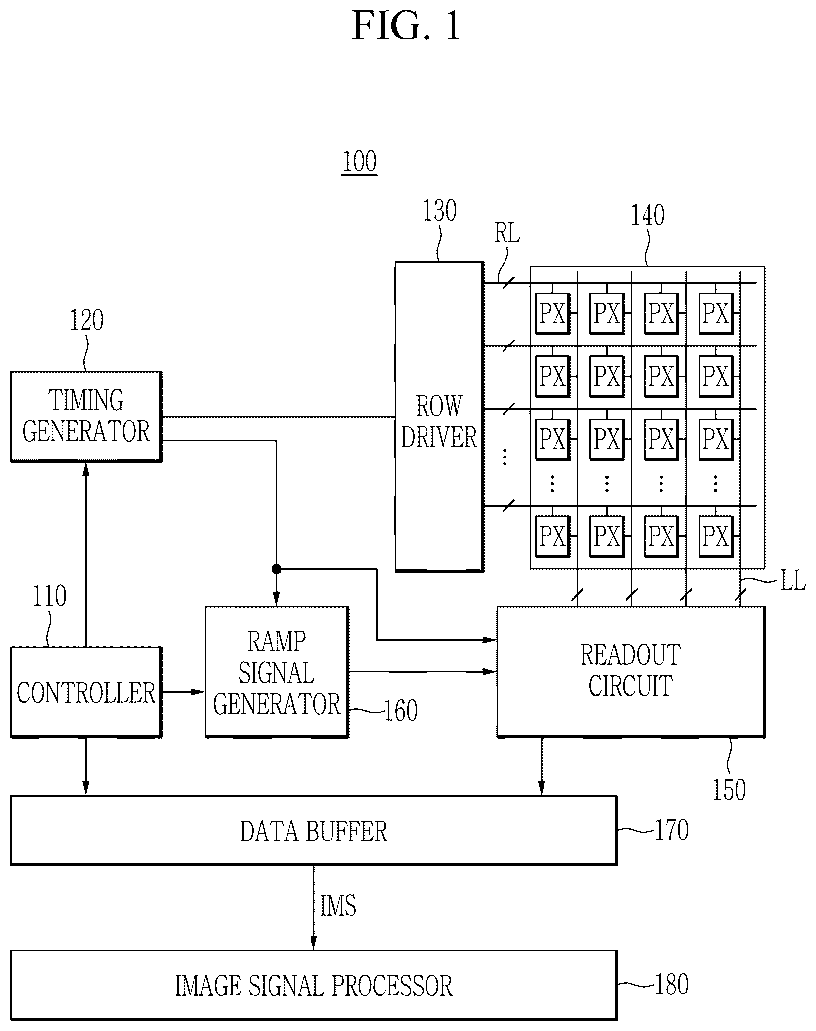
The above and other aspects, features, and advantages of certain embodiments of the present disclosure may be more apparent from the following description taken in conjunction with the accompanying drawings, in which: shows a block diagram of an image sensor, according to an embodiment; shows a circuit diagram of a pixel group of an image sensor, according to an embodiment; shows a top plan view of a pixel group of an image sensor, according to an embodiment; shows a layout of a pixel group of an image sensor, according to an embodiment; shows a layout of an active pattern and a gate layer of , according to an embodiment; shows a layout of an active pattern and a first metal layer of , according to an embodiment; A to C show partially enlarged diagrams of a predetermined region of , according to some embodiments; shows a cross-sectional view with respect to a line A-A′ of A , according to an embodiment; shows a cross-sectional view with respect to a line B-B′ of A , according to an embodiment; and show layouts of a pixel group of an image sensor, according to some embodiments; and shows plan views of a micro lens of an image, sensor, according to an embodiment; and shows plan views of a color filter of an image sensor, according to an embodiment; and to show various examples of an electronic device to which image sensors are applied, according to some embodiments.
DETAILED DESCRIPTION
In the following detailed description, only certain embodiments of the present disclosure have been shown and described, simply by way of illustration. As those skilled in the art would realize, the described embodiments may be modified in various different ways, all without departing from the spirit or scope of the present disclosure. The drawings and description are to be regarded as illustrative in nature and not restrictive, and like reference numerals may designate like elements throughout the specification. The size and thickness of configurations shown in the drawings may be arbitrarily shown for better understanding and ease of description. However, the present disclosure is not limited thereto. In the drawings, the thickness of layers, films, panels, regions, and the like, may be enlarged for clarity. The thicknesses of some layers and areas may be exaggerated for convenience of explanation. It is to be understood that when an element such as, but not limited to, a layer, film, region, or substrate is referred to as being “on” another element, the element may be directly on the other element or intervening elements may also be present. Alternatively or additionally, when an element is referred to as being “directly on” another element, there may be no intervening elements present. As used herein, the terms “on” or “above” may refer to an element being positioned on or below the object portion, and may not necessarily refer to being positioned on the upper side of the object portion based on a gravitational direction. Unless explicitly described to the contrary, the word “comprise”, and variations such as “comprises” or “comprising”, are to be understood to imply the inclusion of stated elements but not the exclusion of any other elements. As used herein, the phrase “in a plan view” may refer to viewing an object portion from the top, and the phrase “in a cross-sectional view” may refer to viewing a cross-section of which the object portion is vertically cut from the side. It is to be understood that a singular form of a noun corresponding to an item may include one or more of the things, unless the relevant context clearly indicates otherwise. As used herein, each of such phrases as “A or B,” “at least one of A and B,” “at least one of A or B,” “A, B, or C,” “at least one of A, B, and C,” and “at least one of A, B, or C,” may include any one of, or all possible combinations of the items enumerated together in a corresponding one of the phrases. As used herein, such terms as “1st” and “2nd,” or “first” and “second” may be used to simply distinguish a corresponding component from another, and may not limit the components in other aspect (e.g., importance or order). It is to be understood that if an element (e.g., a first element) is referred to, with or without the term “operatively” or “communicatively”, as “coupled with,” “coupled to,” “connected with,” or “connected to” another element (e.g., a second element), it may indicate that the element may be coupled with the other element directly (e.g., wired), wirelessly, or via a third element. Reference throughout the present disclosure to “one embodiment,” “an embodiment,” “an example embodiment,” or similar language may indicate that a particular feature, structure, or characteristic described in connection with the indicated embodiment is included in at least one embodiment of the present solution. Thus, the phrases “in one embodiment”, “in an embodiment,” “in an example embodiment,” and similar language throughout this disclosure may, but do not necessarily, all refer to the same embodiment. The embodiments herein may be described and illustrated in terms of blocks, as shown in the drawings, which carry out a described function or functions. These blocks, which may be referred to herein as units or modules or the like, or by names such as device, logic, circuit, controller, counter, comparator, generator, converter, or the like, may be physically implemented by analog and/or digital circuits including one or more of a logic gate, an integrated circuit, a microprocessor, a microcontroller, a memory circuit, a passive electronic component, an active electronic component, an optical component, and the like. As used herein, each of the terms “AIO”, “HfO”, “GaAs”, “GaSb”, “InAs”, “InP”, “InSb”, “PbTe”, “SiGe”, “SiO”, “SiON”, “SiN”, and the like may refer to a material made of elements included in each of the terms and is not a chemical formula representing a stoichiometric relationship. Hereinafter, various embodiments of the present disclosure are described with reference to the accompanying drawings. An image sensor, according to one or more embodiments, is described with reference to to . shows a block diagram of an image sensor, according to an embodiment. Referring to , the image sensor 100 may include a pixel array 140 and a logic circuit for controlling the pixel array 140 . The logic circuit may control the pixel array 140 , and may include, for example, a controller 110 , a timing generator 120 , a row driver 130 , a readout circuit 150 , a ramp signal generator 160 , and a data buffer 170 . The image sensor 100 may further include an image signal processor 180 . In some embodiments, the image signal processor 180 may be disposed outside the image sensor 100 . The image sensor 100 may generate image signals IMS by converting light received from the outside into electrical signals. The image signals IMS may be provided to the image signal processor 180 . The image sensor 100 may be mounted on an electronic device having an image and/or light sensing function. For example, the image sensor 100 may be mounted on an electronic device such as, but not limited to, a camera, a smartphone, a wearable device, an Internet of things (IoT) device, a home appliance, a tablet personal computer (PC), a navigation device, a drone, an advanced driver assistance system (ADAS), and the like. Further, the image sensor 100 may be mounted on the electronic device and may be provided as a component in a vehicle, furniture, a manufacturing facility, a door, various measurement devices, and the like. The pixel array 140 may include pixels PX, and row lines RL and column lines CL that may be respectively connected to the pixels PX. In an embodiment, each of the pixels PX may include at least one photodiode (not shown). The photodiode may sense incident light, and may convert the incident light into electrical signals according to an amount of the light. That is, the photodiode may generate analog pixel signals based on the amount of incident light. The photodiode may be and/or may include a photodiode (e.g., photodiodes PD of ), a pinned diode, and the like. Alternatively or additionally, the photodiode may be and/or may include a single-photon avalanche diode (SPAD) that may be applied to a 3D sensor pixel. The level of the analog pixel signal output from the photodiode may be proportional to an amount of charges output from the photodiode. That is, the level of the analog pixel signal output from the photodiode may be determined according to an amount of light received into the pixel array 140 . The row lines RL may be connected (e.g., coupled) to the pixels PX. For example, a control signal output to the row line RL from the row driver 130 may be transmitted to a gate of a transistor of the pixels PX connected to the corresponding row line RL. The column lines CL may cross the row lines RL and may be connected (e.g., coupled) to the pixels PX. The analog pixel signals output by the pixels PX may be transmitted to the readout circuit 150 through the column lines CL. In an embodiment, the pixels PX may be disposed along the columns and the rows, and each pixel PX may output an analog pixel signal. However, the present disclosure is not limited thereto, and numerous variations may be possible. For example, the pixels PX may be grouped in the form of columns and rows to configure one unit pixel. One unit pixel may include the pixels PX arranged in the form of two columns and two rows, and one unit pixel may output the analog pixel signal. The controller 110 may control operation timings of the above-described constituent elements (e.g., timing generator 120 , row driver 130 , readout circuit 150 , ramp signal generator 160 , and data buffer 170 ) by using control signals. In an embodiment, the controller 110 may receive a mode signal indicating an imaging mode from an application processor (e.g., image signal processor 180 ), and may control overall operation of the image sensor 100 based on the received mode signal. For example, the application processor may determine the imaging mode of the image sensor 100 according to various scenarios such as, but not limited to, illumination of the imaging environment, user's resolution setting, a sensed and/or learned state, and the like, and may provide the determined result to the controller 110 as a mode signal. The controller 110 may control the pixels PX of the pixel array 140 to output analog pixel signals according to the imaging mode. The pixel array 140 may output analog pixel signals for the respective pixels PX and/or analog pixel signals for some of the pixels PX. The readout circuit 150 may sample and/or process the analog pixel signals transmitted from the pixel array 140 . The timing generator 120 may generate a signal serving as a reference for the operation timing of the components of the image sensor 100 . For example, the timing generator 120 may control the timings of the row driver 130 , the readout circuit 150 , and the ramp signal generator 160 . The timing generator 120 may provide control signals for controlling the timings of the row driver 130 , the readout circuit 150 , and the ramp signal generator 160 . The row driver 130 may generate a control signal for driving the pixel array 140 in response to the control signal of the timing generator 120 , and may provide control signals to the pixels PX of the pixel array 140 through the row lines RL. In an embodiment, the row driver 130 may control the pixel PX to sense incident light for each row line unit. The row line unit may include at least one row line RL. For example, the row driver 130 may generate a transmission signal for controlling a transmission transistor, a reset control signal for controlling a reset transistor, and/or a selection control signal for controlling a selection transistor to provide the generated signals to the pixel array 140 . The readout circuit 150 may convert the analog pixel signal (or electrical signal) from the pixel PX connected to the row line RL selected from among the pixels PX, in response to the control signal from the timing generator 120 , into a pixel value representing the amount of light. The readout circuit 150 may convert the analog pixel signal output through the corresponding column line CL into a pixel value. For example, the readout circuit 150 may convert the analog pixel signal into the pixel value by comparing the ramp signal and the pixel signal. The pixel value may be and/or may include image data having bits. That is, the readout circuit 150 may include at least one of a selector, comparators, and counter circuits to convert the analog pixel signal into a pixel value. The ramp signal generator 160 may generate reference signals and may transmit the reference signals to the readout circuit 150 . The ramp signal generator 160 may include at least one of a current source, a resistor, and a capacitor to generate the reference signals. For example, the ramp signal generator 160 may adjust a ramp voltage applied to a ramp resistor by adjusting a current amount of a variable current source and/or resistance of a variable resistor, and may generate ramp signals that may fall and/or rise with a slope determined according to the current amount of the variable current source and/or the resistance of the variable resistor. The data buffer 170 may store pixel values of the pixels PX connected to the selected column line CL transmitted from the readout circuit 150 , and may output the stored pixel values (e.g., image signal IMS) in response to an enable signal from the controller 110 . The image signal processor 180 may perform image signal processing on the image signal IMS received from the data buffer 170 . For example, the image signal processor 180 may receive image signals IMS from the data buffer 170 , and may synthesize the received image signals to generate an image. shows a circuit diagram of a pixel group of an image sensor, according to an embodiment. Referring to , pixel groups PXG of the image sensor 100 may include sub-pixel groups (e.g., a first sub-pixel group SPX 1 , a second sub-pixel group SPX 2 , a third sub-pixel group SPX 3 , and a fourth sub-pixel group SPX 4 ), selection transistors (e.g., a first selection transistor SELT 1 and a second selection transistor SELT 2 ) connected to the first to fourth sub-pixel groups SPX 1 to SPX 4 , and source follower transistors (e.g., a first source follower transistor SFT 1 and a second source follower transistor SFT 2 ) connected between the first to fourth sub-pixel groups SPX 1 to SPX 4 and the first and second selection transistors SELT 1 and SELT 2 . The first and second source follower transistors SFT 1 and SFT 2 may receive a same gate signal and a same pixel power source voltage. The first selection transistor SELT 1 may be connected to the first source follower transistor SFT 1 and the second selection transistor SELT 2 may be connected to the second source follower transistor SFT 2 . Output terminals of the first selection transistor SELT 1 and the second selection transistor SELT 2 may be connected to each other. The respective pixel groups PXG of the image sensor 100 may further include a reset transistor RT, a first conversion transistor DCT 1 , and a second conversion transistor DCT 2 . The first sub-pixel group SPX 1 may include a first photodiode PD 1 , a second photodiode PD 2 , and a first transmission transistor TT 1 and a second transmission transistor TT 2 that may be respectively connected to the first photodiode PD 1 and the second photodiode PD 2 . The first photodiode PD 1 and the second photodiode PD 2 may respectively generate photocharges (hereinafter referred to as charges) corresponding to the received amount of light. The first photodiode PD 1 and the second photodiode PD 2 may be respectively connected to the first transmission transistor TT 1 and the second transmission transistor TT 2 . The first transmission transistor TT 1 and the second transmission transistor TT 2 of the first sub-pixel group SPX 1 may be respectively turned on in response to active levels (e.g., logic high) of the transmission signals TS 1 and TS 2 . The first photodiode PD 1 may be mainly described, and the description given below may be substantially equivalently applied to the remaining photodiodes (e.g., second photodiode PD 2 , third photodiode PD 3 , fourth photodiode PD 4 , fifth photodiode PD 5 , sixth photodiode PD 6 , seventh photodiode PD 7 , and eighth photodiode PD 8 ) of the pixel groups PXG. In an embodiment, the first photodiode PD 1 may generate charges according to the receiving amount of light and may store the charges. The first photodiode PD 1 may include an anode connected to a ground and a cathode connected to a first end of the first transmission transistor TT 1 . A first transmission signal TS 1 may be supplied to a first transmission gate TG 1 of the first transmission transistor TT 1 , and a first end of the first transmission transistor TT 1 may be connected to a first floating diffusion region (e.g., a first floating diffusion region FD 1 of ). When the first transmission transistor TT 1 is turned on by the first transmission signal TS 1 , the charges stored in the first photodiode PD 1 may be transmitted to the first floating diffusion region. The first floating diffusion region FD 1 may maintain the charges transmitted from the first photodiode PD 1 . The second sub-pixel group SPX 2 may include the third photodiode PD 3 , the fourth photodiode PD 4 , and a third transmission transistor TT 3 and a fourth transmission transistor TT 4 that may be respectively connected to the third photodiode PD 3 and the fourth photodiode PD 4 . The third transmission transistor TT 3 and the fourth transmission transistor TT 4 of the second sub-pixel group SPX 2 may be respectively turned on in response to an active level (e.g., logic high) of the transmission signals TS 3 and TS 4 . The third sub-pixel group SPX 3 may include the fifth photodiode PD 5 , the sixth photodiode PD 6 , and a fifth transmission transistor TT 5 and a sixth transmission transistor TT 6 that may be respectively connected to the fifth photodiode PD 5 and the sixth photodiode PD 6 . The fifth transmission transistor TT 5 and the sixth transmission transistor TT 6 of the third sub-pixel group SPX 3 may be respectively turned on in response to the active level (e.g., logic high) of the transmission signals TS 5 and TS 6 . The fourth sub-pixel group SPX 4 may include the seventh photodiode PD 7 , the eighth photodiode PD 8 , and a seventh transmission transistor TT 7 and an eighth transmission transistor TT 8 respectively connected to the seventh photodiode PD 7 and the eighth photodiode PD 8 . The seventh transmission transistor TT 7 and the eighth transmission transistor TT 8 of the fourth sub-pixel group SPX 4 may be respectively turned on in response to the active level (e.g., logic high) of the transmission signals TS 7 and TS 8 . The transmission signals (e.g., the first transmission signal TS 1 , a second transmission signal TS 2 , a third transmission signal TS 3 , a fourth transmission signal TS 4 , fifth transmission signal TS 5 , a sixth transmission signal TS 6 , a seventh transmission signal TS 7 , and an eighth transmission signal TS 8 may have the active level at the same time and/or different times, according to a reading mode. For example, in a first reading mode, the first to eighth transmission signals TS 1 to TS 8 may be different from each other and may have the active level at different times. In a second reading mode (e.g., a charge summing mode), the first to eighth transmission signals TS 1 to TS 8 may be the same and/or substantially similar signals and may have the active level at the same and/or substantially similar time. In a third reading mode, the first and second transmission signals TS 1 and TS 2 of the first sub-pixel group SPX 1 may be the same and/or substantially similar signals, the third and fourth transmission signals TS 3 and TS 4 of the second sub-pixel group SPX 2 may be the same and/or substantially similar signals, the fifth and sixth transmission signals TS 5 and TS 6 of the third sub-pixel group SPX 3 may be the same and/or substantially similar signals, and the seventh and eighth transmission signals TS 7 and TS 8 of the fourth sub-pixel group SPX 4 may be the same and/or substantially similar signals. However, the present disclosure is not limited thereto, and the first to eighth transmission signals TS 1 to TS 8 may have different configurations according to the same and/or different reading modes. The first to eighth transmission transistors TT 1 to TT 8 respectively provided to the first to fourth sub-pixel groups SPX 1 to SPX 4 may be turned on and may transmit the charges generated by the corresponding photodiode PD to the first floating diffusion node FN 1 . The first to fourth sub-pixel groups SPX 1 to SPX 4 may respectively include floating diffusion regions (e.g., a first floating diffusion region FD 1 , a second floating diffusion region FD 2 , a third floating diffusion region FD 3 , a fourth floating diffusion region FD 4 , a fifth floating diffusion region FD 5 , a sixth floating diffusion region FD 6 , a seventh floating diffusion region FD 7 , and an eighth floating diffusion region FD 8 of ). The first to eighth floating diffusion regions FD 1 to FD 8 may be electrically connected to each other through the floating connection wire FWR. As shown in , the first to eighth photodiodes PD 1 to PD 8 may be connected to the first floating diffusion node FN 1 . Although shows that eight photodiodes are connected to the first floating diffusion node FN 1 , it is to be understood that such configuration is shown by way of non-limiting example. That is, the number of the photodiodes PD connected to the first floating diffusion node FN 1 may be modified in many ways without departing from the scope of the present disclosure. The first conversion transistor DCT 1 and the second conversion transistor DCT 2 may be connected between the reset transistor RT and the first floating diffusion node FN 1 . The first conversion transistor DCT 1 and the second conversion transistor DCT 2 may respectively include a first conversion gate DCG 1 and a second conversion gate DCG 2 for respectively receiving a first conversion signal DCS 1 and a second conversion signal DCS 2 . The first conversion transistor DCT 1 may be connected between the first floating diffusion node FN 1 and a second floating diffusion node FN 2 . The first conversion transistor DCT 1 may electrically connect the first floating diffusion node FN 1 and the second floating diffusion node FN 2 in response to the active level of the first conversion signal DCS 1 . A first expanding metal pattern EP 1 may be connected to the second floating diffusion node FN 2 . In an embodiment, the first expanding metal pattern EP 1 may configure a capacitor with other wires. The second conversion transistor DCT 2 may be connected between the second floating diffusion node FN 2 and a third floating diffusion node FN 3 . The second conversion transistor DCT 2 may electrically connect the second floating diffusion node FN 2 and the third floating diffusion node FN 3 in response to the active level of the second conversion signal DCS 2 . A second expanding metal pattern EP 2 may be connected to the third floating diffusion node FN 3 . In an embodiment, the second expanding metal pattern EP 2 may configure a capacitor with other wires. The reset transistor RT may be connected between the third floating diffusion node FD 3 and a pixel power source voltage wire V Pix . The first conversion transistor DCT 1 may be coupled in series to the second conversion transistor DCT 2 through the second floating diffusion node FN 2 , and the second conversion transistor DCT 2 may be coupled in series to the reset transistor RT through the third floating diffusion node FN 3 . As a result, the first conversion transistor DCT 1 , the second conversion transistor DCT 2 , and the reset transistor RT may be coupled in series. The reset transistor RT may include a reset gate electrode RG for receiving a reset signal RS. The reset transistor RT may be turned on in response to the active level of the reset signal RS applied to the reset gate electrode RG, and may periodically and/or aperiodically reset the charges stored in the first floating diffusion node FN 1 , the second floating diffusion node FN 2 , and the third floating diffusion node FN 3 . That is, when the reset transistor RT, the first conversion transistor DCT 1 , and the second conversion transistor DCT 2 are turned on, the pixel power source voltage V Pix may be transmitted to the first floating diffusion node FN 1 , the second floating diffusion node FN 2 , and the third floating diffusion node FN 3 . Accordingly, the charges stored in the first floating diffusion node FN 1 , the second floating diffusion node FN 2 , and the third floating diffusion node FN 3 may be discharged, and the first floating diffusion node FN 1 , the second floating diffusion node FN 2 , and the third floating diffusion node FN 3 may be reset. The first conversion transistor DCT 1 and the second conversion transistor DCT 2 may respectively vary a conversion gain of the pixel group PXG by varying a capacitance of the first floating diffusion node FN 1 in response to the active level of the first conversion signal DCS 1 and the second conversion signal DCS 2 . For example, when the images are photographed (e.g., captured), light with low intensity of illumination and high intensity of illumination may be concurrently input to the pixel group PXG, and/or strong light and weak light may be simultaneously input to the pixel group PXG. Accordingly, the conversion gains of the respective pixels may be variable by the incident light. That is, the first conversion transistor DCT 1 and the second conversion transistor DCT 2 may be turned off and the pixel group PXG may have a first conversion gain, and the first conversion transistor DCT 1 may be turned on and may have a second conversion gain that may be greater than the first conversion gain. Alternatively or additionally, the first conversion transistor DCT 1 and the second conversion transistor DCT 2 may be turned on and may have a third conversion gain that may be greater than the second conversion gain. According to operations of the first conversion transistor DCT 1 and the second conversion transistor DCT 2 , different conversion gains may be provided in the first conversion gain mode (e.g., high intensity of illumination mode) and the second to third conversion gain modes (e.g., low intensity of illumination modes). That is, when the first conversion transistor DCT 1 and the second conversion transistor DCT 2 are turned on, a capacitance of the first floating diffusion node FN 1 , the second floating diffusion node FN 2 , and the third floating diffusion node FN 3 may increase and the conversion gain may be reduced. Alternatively or additionally, when the first conversion transistor DCT 1 and the second conversion transistor DCT 2 are turned off, a capacitance of the first floating diffusion node FN 1 , the second floating diffusion node FN 2 , and the third floating diffusion node FN 3 may be reduced and the conversion gain may increase. The first source follower transistor SFT 1 and the second source follower transistor SFT 2 may respectively include a first source follower gate SF 1 and a second source follower gate SF 2 , and the first source follower gate SF 1 may be connected to the second source follower gate SF 2 by one node. The first source follower gate SF 1 and the second source follower gate SF 2 may be connected to the first floating diffusion node FN 1 . The first source follower transistor SFT 1 and the second source follower transistor SFT 2 may output an analog pixel signal according to a voltage at the first floating diffusion node FN 1 . The pixel power source voltage V Pix may be applied to first ends of the first source follower transistor SFT 1 and the second source follower transistor SFT 2 , and second ends of the first source follower transistor SFT 1 and the second source follower transistor SFT 2 may be connected to first ends of the first selection transistor SELT 1 and the second selection transistor SELT 2 . That is, the first source follower transistor SFT 1 may include a first sharing source region SS 1 sharing a source region with the first selection transistor SELT 1 and a drain region connected to the pixel power source voltage V Pix . The second source follower transistor SFT 2 may include a second sharing source region SS 2 sharing the source region with the second selection transistor SELT 2 and a drain region connected to the pixel power source voltage V Pix . Hence, the first source follower transistor SFT 1 may be connected to the first selection transistor SELT 1 through the first sharing source region SS 1 , and the second source follower transistor SFT 2 may be connected to the second selection transistor SELT 2 through the second sharing source region SS 2 . The first source follower transistor SFT 1 and the second source follower transistor SFT 2 may configure a source follower circuit, and may output a voltage at a level that may correspond to the charges stored in the first floating diffusion node FN 1 as an analog pixel signal. A first selection gate SEL 1 of the first selection transistor SELT 1 may be connected to a second selection gate SEL 2 of the second selection transistor SELT 2 . Hence, the same selection signal SELS may be applied to the first selection gate SEL 1 and the second selection gate SEL 2 . A first end of the first selection transistor SELT 1 may be connected to the first source follower transistor SFT 1 through the first sharing source region SS 1 , and a second end of the first selection transistor SELT 1 may be connected to an output voltage wire Vout for outputting pixel signals. A first end of the second selection transistor SELT 2 may be connected to the first source follower transistor SFT 1 through the second sharing source region SS 2 , and a second end of the first selection transistor SELT 1 may be connected to the output voltage wire Vout for outputting pixel signals. When the first selection transistor SELT 1 and the second selection transistor SELT 2 are turned on by the selection signal SELS, the analog pixel signals from the first source follower transistor SFT 1 and the second source follower transistor SFT 2 may be transmitted to the readout circuit 150 of through the column line CL. shows a top plan view of a pixel group of an image sensor, according to an embodiment. shows a layout of a pixel group of an image sensor, according to an embodiment. shows a layout of an active pattern and a gate layer of , according to an embodiment. shows a layout of an active pattern and a first metal layer of , according to an embodiment. Referring to to , the pixel group PXG may include first to fourth sub-pixel groups SPX 1 to SPX 4 , first to eighth photodiodes PD 1 to PD 8 , an active pattern ACT, a gate layer GL, and a first metal layer M 1 . The active pattern ACT may be disposed on the first to eighth photodiodes PD 1 to PD 8 , and may include active patterns (e.g., a first active pattern ACT 1 , a second active pattern ACT 2 , a third active pattern ACT 3 , a fourth active pattern ACT 4 , a fifth active pattern ACT 5 , and a sixth pattern ACT 6 ). The first to sixth active pattern may be disposed on the same layer. The gate layer GL may be disposed on the active pattern ACT and may include a first selection gate SEL 1 , a second selection gate SEL 2 , a source follower gate SF, a first conversion gate DCG 1 , a second conversion gate DCG 2 , a dummy gate DMY_G, and first to eighth transmission gates (e.g., the first transmission gate TG 1 , a second transmission gate TG 2 , a third transmission gate TG 3 , a fourth transmission gate TG 4 , a fifth transmission gate TG 5 , a sixth transmission gate TG 6 , a seventh transmission gate TG 7 , and an eighth transmission gate TG 8 ). The first to eighth transmission gates may be disposed on the same and/or a substantially similar layer. The first metal layer M 1 may be disposed on the gate layer GL and may include a transmission gate wire TWR, a ground wire GWR, a floating connection wire FWR, a first expanding metal pattern EP 1 , a second expanding metal pattern EP 2 , a first conversion gate wire DWR 1 , a second conversion gate wire DWR 2 , a selection gate connection wire SEWR, a reset gate wire RWR, and connection wires (e.g., a first connection wire WR 1 , a second connection wire WR 2 , and a third connection wire WR 3 ). The first to third connection wires may be disposed on the same and/or a substantially similar layer. The first to fourth sub-pixel groups SPX 1 to SPX 4 may be arranged in a two-dimensional way in a first direction X and a second direction Y on a plane. That is, the first to fourth sub-pixel groups SPX 1 to SPX 4 may be arranged in a matrix form. For example, as shown in , the first sub-pixel group SPX 1 and the third sub-pixel group SPX 3 may be arranged in the first direction X, and the first sub-pixel group SPX 1 and the second sub-pixel group SPX 2 may be arranged in the second direction Y. The fourth sub-pixel group SPX 4 may be arranged in the second direction Y with the third sub-pixel group SPX 3 , and may be arranged in the first direction X with the second sub-pixel group SPX 2 . That is, the first sub-pixel group SPX 1 and the fourth sub-pixel group SPX 4 may be arranged in the diagonal direction. However, an arrangement form of the first to fourth sub-pixel groups SPX 1 to SPX 4 is not limited thereto, and may be changed in many ways without departing from the scope of the present disclosure. The first to fourth sub-pixel groups SPX 1 to SPX 4 may include pixels (e.g., a first pixel PX 1 , a second pixel PX 2 , a third pixel PX 3 , a fourth pixel PX 4 , a fifth pixel PX 5 , a sixth pixel PX 6 , a seventh pixel PX 7 , and an eighth pixel PX 8 ) arranged in columns and rows. For example, the first sub-pixel group SPX 1 may include the first pixel PX 1 and the second pixel PX 2 arranged in the first direction X, the second sub-pixel group SPX 2 may include the third pixel PX 3 and the fourth pixel PX 4 arranged in the first direction X, the third sub-pixel group SPX 3 may include the fifth pixel PX 5 and the sixth pixel PX 6 arranged in the first direction X, and the fourth sub-pixel group SPX 4 may include the seventh pixel PX 7 and the eighth pixel PX 8 arranged in the first direction X. The first sub-pixel group SPX 1 may include the first photodiode PD 1 , the second photodiode PD 2 , the first transmission gate TG 1 , the second transmission gate TG 2 , the first floating diffusion region FD 1 , and the second floating diffusion region FD 2 . The second sub-pixel group SPX 2 may include the third photodiode PD 3 , the fourth photodiode PD 4 , the third transmission gate TG 3 , the fourth transmission gate TG 4 , the third floating diffusion region FD 3 , and the fourth floating diffusion region FD 4 . The third sub-pixel group SPX 3 may include the fourth photodiode PD 4 , the fifth photodiode PD 5 , the fourth transmission gate TG 4 , the fifth transmission gate TG 5 , the fifth floating diffusion region FD 5 , and the sixth floating diffusion region FD 6 . The fourth sub-pixel group SPX 4 may include the seventh photodiode PD 7 , an eighth photodiode PD 8 , the seventh transmission gate TG 7 , the eighth transmission gate TG 8 , seventh floating diffusion region FD 7 , and the eighth floating diffusion region FD 8 . The first to eighth photodiodes PD 1 to PD 8 may be divided and disposed in the first direction X in the first to fourth sub-pixel groups SPX 1 to SPX 4 . For example, the third photodiode PD 3 and the fourth photodiode PD 4 may be divided and disposed in the first direction X in the second sub-pixel group SPX 2 . That is, the third photodiode PD 3 and the fourth photodiode PD 4 may be spaced and disposed in the first direction X. The third photodiode PD 3 and the fourth photodiode PD 4 have been described as a reference, and the remaining photodiodes (e.g., PD 1 , PD 2 , PD 5 , PD 6 , PD 7 , and PD 8 ) may have the same and/or a substantially similar arrangement form as the arrangement relationship of the third photodiode PD 3 and the fourth photodiode PD 4 in the sub-pixel groups SPX 1 , SPX 3 , and SPX 4 . The first to eighth photodiodes PD 1 to PD 8 may respectively include two short sides extending in the first direction X and two long sides extending in the second direction Y, and may respectively have a rectangular shape in a plan view. However, the respective shapes of the first to eighth photodiodes PD 1 to PD 8 on the plane may not be limited thereto and may be modifiable in many ways without departing from the scope of the present disclosure. The pixel separating pattern DTI may be disposed between the photodiodes PD. The pixel separating pattern DTI may have a lattice shape in a plan view, may be disposed between the photodiodes PD, and may define the first to fourth sub-pixel groups SPX 1 to SPX 4 . That is, the pixel separating pattern DTI may include a horizontal pixel separating pattern DTI_H extending in the first direction X and a vertical pixel separating pattern DTI_V extending in the second direction Y crossing the first direction X. As the horizontal pixel separating pattern DTI_H and the vertical pixel separating pattern DTI_V are disposed between the photodiodes PD, the pixel separating pattern DTI may define lateral sides of the respective short sides and long sides of the photodiodes PD and may have a lattice shape in a plan view. A portion of the pixel separating pattern DTI may be separated and disposed in the second direction Y. That is, a portion of the pixel separating pattern DTI may be separated and disposed in the second direction Y among the photodiodes PD. For example, a first part of the vertical pixel separating pattern DTI_V from among the pixel separating pattern DTI may be spaced in the second direction Y, among the photodiodes PD, from a second part of the vertical pixel separating pattern DTI_V, such that a separating region DCC may be defined between the first part and the second part of the vertical pixel separating pattern DTI_V. However, without being limited thereto, a first part of the horizontal pixel separating pattern DTI_H may be separated in the first direction X, among the photodiodes PD, from a second part of the horizontal pixel separating pattern DTI_H, such that the separating region DCC may be defined between the first part and the second part of the horizontal pixel separating pattern DTI_H. The separating region DCC may be disposed among the photodiodes PD. In an embodiment, the separating region DCC may be substantially disposed in a center of the respective first to fourth sub-pixel groups SPX 1 to SPX 4 . That is, the separating region DCC may be disposed in parallel to a center of the photodiodes PD in the first direction X among the photodiodes PD disposed in the respective first to fourth sub-pixel groups SPX 1 to SPX 4 . In other words, the separating region DCC may be disposed in a center of a border among the photodiodes PD. For example, the separating region DCC may be substantially disposed in the center of the first sub-pixel group SPX 1 . The separating region DCC may be disposed in parallel to the centers of the first photodiode PD 1 and the second photodiode PD 2 in the first direction X. However, the position (location) of the separating region DCC is not limited thereto, and may be changed in many ways without departing from the scope of the present disclosure. In some embodiments, the separating region DCC may be disposed on a portion that is not the center in the first to fourth sub-pixel groups SPX 1 to SPX 4 . In some embodiments, some of the separating regions DCC may be substantially disposed in the respective centers of the first to fourth sub-pixel groups SPX 1 to SPX 4 , and others thereof may be disposed in other portions, that are not the centers, of the first to fourth sub-pixel groups SPX 1 to SPX 4 . The first pixel PX 1 and the second pixel PX 2 of the first sub-pixel group SPX 1 may respectively include one photodiode and one transmission gate. For example, the first pixel PX 1 of the first sub-pixel group SPX 1 may include the first photodiode PD 1 and the first transmission gate TG 1 . The second pixel PX 2 may include the second photodiode PD 2 and the second transmission gate TG 2 . The third pixel PX 3 of the second sub-pixel group SPX 2 may include the third photodiode PD 3 and the third transmission gate TG 3 . The fourth pixel PX 4 may include the fourth photodiode PD 4 and the fourth transmission gate TG 4 . The fifth pixel PX 5 of the third sub-pixel group SPX 3 may include the fifth photodiode PD 5 and the fifth transmission gate TG 5 . The sixth pixel PX 6 may include the sixth photodiode PD 6 and the sixth transmission gate TG 6 . The seventh pixel PX 7 of the fourth sub-pixel group SPX 4 may include the seventh photodiode PD 7 and the seventh transmission gate TG 7 . The eighth pixel PX 8 may include the eighth photodiode PD 8 and the eighth transmission gate TG 8 . The first to eighth transmission gates TG 1 to TG 8 may be respective gates of the first to eighth transmission transistors (e.g., first to eighth transmission transistors TT 1 to TT 8 of ). The first to eighth transmission transistors TT 1 to TT 8 may be respectively connected to the first to eighth photodiodes PD 1 to PD 8 . The active pattern ACT may be disposed on the photodiodes PD, and may overlap the photodiodes PD in the third direction Z. For example, the first active pattern ACT 1 may be disposed on some of the first to fourth sub-pixel groups SPX 1 to SPX 4 . As another example, the first active pattern ACT 1 may be disposed in the second sub-pixel group SPX 2 . The first active pattern ACT 1 may overlap at least some of the photodiodes PD. That is, a portion of the first active pattern ACT 1 may overlap the photodiodes PD in the third direction Z, and the remaining portion of the first active pattern ACT 1 may not overlap the photodiodes PD and may be disposed in the separating region DCC defined by the vertical pixel separating pattern DTI_V separated in the second direction Y. The first active pattern ACT 1 overlapping the photodiodes PD and the first active pattern ACT 1 disposed in the separating region DCC may be integrally formed. For example, a portion of the first active pattern ACT 1 disposed on one side of the separating region DCC in the first direction X may overlap the third photodiode PD 3 in the third direction Z, and a portion of the first active pattern ACT 1 disposed on the other side of the separating region DCC in the first direction X may overlap the fourth photodiode PD 4 in the third direction Z. A portion of the first active pattern ACT 1 disposed in the separating region DCC may not overlap the third photodiode PD 3 and the fourth photodiode PD 4 . Hence, a portion of the first active pattern ACT 1 may be substantially disposed in the center of the second sub-pixel group SPX 2 . The second active pattern ACT 2 may be disposed in some of the first to fourth sub-pixel groups SPX 1 to SPX 4 . For example, the second active pattern ACT 2 may overlap the first sub-pixel group SPX 1 of another pixel group PXG. The second active pattern ACT 2 may be spaced from the first active pattern ACT 1 in the second direction Y with the horizontal pixel separating pattern DTI_H therebetween. That is, the first active pattern ACT 1 and the second active pattern ACT 2 may have a symmetric shape in the second direction Y with the horizontal pixel separating pattern DTI_H therebetween. The second active pattern ACT 2 may overlap at least some of the photodiodes PD. That is, a portion of the second active pattern ACT 2 may overlap the photodiodes PD in the third direction Z, and another portion of the second active pattern ACT 2 may not overlap the photodiodes PD and may be disposed in the separating region DCC defined by the vertical pixel separating pattern DTI_V separated and disposed in the second direction Y. The second active pattern ACT 2 overlapping the photodiodes PD and the second active pattern ACT 2 disposed in the separating region DCC may be integrally formed. For example, a portion of the second active pattern ACT 2 disposed on the one side of the separating region DCC in the first direction X may overlap the first photodiode PD 1 in the third direction Z, and a portion of the second active pattern ACT 2 disposed on the other side of the separating region DCC in the first direction X may overlap the second photodiode PD 2 in the third direction Z. A portion of the second active pattern AC 2 disposed in the separating region DCC may not overlap the first photodiode PD 1 and the second photodiode PD 2 . Hence, a portion of the second active pattern ACT 2 may be substantially disposed in the center of the first sub-pixel group SPX 1 . The first selection gate SEL 1 may be disposed in the first active pattern ACT 1 . The first selection gate SEL 1 may be a gate of the first selection transistor (e.g., first selection transistor SELT 1 of ). The first selection gate SEL 1 may be disposed on the first active pattern ACT 1 , and may configure the first selection transistor SELT 1 with an extrinsic region doped to the first active pattern ACT 1 . The first selection gate SEL 1 may overlap a portion of the first active pattern ACT 1 disposed on the one side of the separating region DCC in the first direction X, in the third direction Z. For example, the first selection gate SEL 1 may be disposed on the first active pattern ACT 1 overlapping the third photodiode PD 3 in the third sub-pixel group SPX 2 . The second selection gate SEL 2 may be disposed on the second active pattern ACT 2 . The second selection gate SEL 2 may be a gate of the second selection transistor (e.g., second selection transistor SELT 2 of ). The second selection gate SEL 2 may be disposed on the second active pattern ACT 2 , and may configure the second selection transistor SELT 2 with an extrinsic region doped to the second active pattern ACT 2 . The second selection gate SEL 2 may overlap a portion of the second active pattern ACT 2 disposed on the one side of the separating region DCC in the first direction X, in the third direction Z. The second selection gate SEL 2 may be spaced from the first selection gate SEL 1 in the second direction Y with the horizontal pixel separating pattern DTI_H therebetween. That is, the second selection gate SEL 2 may be disposed to be symmetric with the first selection gate SEL 1 with the horizontal pixel separating pattern DTI_H therebetween. For example, the second selection gate SEL 2 may be disposed in the second active pattern ACT 2 overlapping the first photodiode PD 1 on the first sub-pixel group SPX 1 . A source follower gate SF may be disposed on the first active pattern ACT 1 and the second active pattern ACT 2 . That is, the source follower gate SF may extend in the second direction Y to reach the second active pattern ACT 2 from the first active pattern ACT 1 . The source follower gate SF may cross the horizontal pixel separating pattern DTI_H, and may extend in the second direction Y to the second active pattern ACT 2 from the first active pattern ACT 1 . Accordingly, at least a portion of the source follower gate SF may be disposed on the horizontal pixel separating pattern DTI_H, and may overlap the horizontal pixel separating pattern DTI_H in the third direction Z. The source follower gate SF may include a first source follower gate SF 1 disposed on the first active pattern ACT 1 and a second source follower gate SF 2 disposed on the second active pattern ACT 2 . That is, the first source follower gate SF 1 and the second source follower gate SF 2 may be integrally formed. The first source follower gate SF 1 and the second source follower gate SF 2 may respectively be gates of the first source follower transistor (e.g., first source follower transistor SFT 1 of ) and the second source follower transistor (e.g., second source follower transistor SFT 2 of ). The first source follower gate SF 1 may be disposed on the first active pattern ACT 1 , and may configured the first source follower transistor SFT 1 with an extrinsic region doped to the first active pattern ACT 1 . The second source follower gate SF 2 may be disposed on the second active pattern ACT 2 , and may configure the first source follower transistor SFT 1 with an extrinsic region doped to the second active pattern ACT 2 . The first source follower gate SF 1 may overlap a portion of the first active pattern ACT 1 disposed on the other side of the separating region DCC in the first direction X, in the third direction Z. That is, the first source follower gate SF 1 may be spaced from the first selection gate SEL 1 in the first direction X with the vertical pixel separating pattern DTI_V therebetween. For example, the first source follower gate SF 1 may be disposed on the first active pattern ACT 1 overlapping the fourth photodiode PD 4 in the third sub-pixel group SPX 3 . Accordingly, the first source follower transistor SFT 1 may be connected to the first selection transistor SELT 1 through the first active pattern ACT 1 . The second source follower gate SF 2 may overlap a portion of the second active pattern ACT 2 disposed on the other side of the separating region DCC in first direction X, in the third direction Z. That is, the second source follower gate SF 2 may be spaced from the second selection gate SEL 2 in the first direction X with the vertical pixel separating pattern DTI_V therebetween. For example, the second source follower gate SF 2 may be disposed on the second active pattern ACT 2 overlapping the second photodiode PD 2 in the first sub-pixel group SPX 1 . Hence, the second source follower transistor SFT 2 may be connected to the second selection transistor SELT 2 through the second active pattern ACT 2 . The first selection gate SEL 1 may be connected to the second selection gate SEL 2 through the selection gate connection wire SEWR. One side end of the selection gate connection wire SEWR may be connected to the first selection gate SEL 1 through the first selection gate contact CT_SEL 1 . The first selection gate contact CT_SEL 1 may overlap the center of the first selection gate SEL 1 , but is not limited thereto. The other side end of the selection gate connection wire SEWR may be connected to the second selection gate SEL 2 through the second selection gate contact CT_SEL 2 . The second selection gate contact CT_SEL 2 may overlap the center of the second selection gate SEL 2 , but is not limited thereto. A portion of the selection gate connection wire SEWR may be disposed on the first selection gate SEL 1 and the second selection gate SEL 2 and may extend in the first direction X. Another portion of the selection gate connection wire SEWR may extend in the second direction Y on the pixel separating pattern DTI. The first connection wire WR 1 may extend in the second direction Y to reach the second active pattern ACT 2 from the first active pattern ACT 1 and may connect the first active pattern ACT 1 and the second active pattern ACT 2 . That is, the first connection wire WR 1 may be connected to a portion of the first active pattern ACT 1 disposed on one side of the first selection gate SEL 1 through a first contact CT 1 , and the first connection wire WR 1 may be connected to a portion of the second active pattern ACT 2 disposed on one side of the second selection gate SEL 2 through a second contact CT 2 . The second connection wire WR 2 may extend in the second direction Y to reach the second active pattern ACT 2 from the first active pattern ACT 1 and may connect the first active pattern ACT 1 and the second active pattern ACT 2 . That is, the second connection wire WR 2 may be connected to a portion of the first active pattern ACT 1 disposed on one side of the active pattern first source follower gate SF 1 through the third contact CT 3 , and the active pattern second connection wire WR 2 may be connected to a portion of the second active pattern ACT 2 disposed on one side of the second source follower gate SF 2 through the fourth contact CT 4 . A relationship between the first source follower transistor SFT 1 and the first selection transistor SELT 1 and a relationship between the second source follower transistor SFT 2 and the second selection transistor SELT 2 are described with reference to A to C . The third active pattern ACT 3 may be spaced from the first active pattern ACT 1 in the first direction X with the vertical pixel separating pattern DTI_V therebetween. That is, the first active pattern ACT 1 and the third active pattern ACT 3 may have symmetric shapes in the first direction X with the vertical pixel separating pattern DTI_V therebetween. Hence, a disposing relationship between the third active pattern ACT 3 and other elements may be substantially equivalent to the disposing relationship between the first active pattern ACT 1 and other elements. Consequently, repeated descriptions may be omitted and differences may be described. The third active pattern ACT 3 may be disposed in some of the first to fourth sub-pixel groups SPX 1 to SPX 4 . For example, the third active pattern ACT 3 may be disposed in the fourth sub-pixel group SPX 4 . A portion of the third active pattern ACT 3 disposed on the one side of the separating region DCC in the first direction X may overlap the seventh photodiode PD 7 in the third direction Z, and a portion of the third active pattern ACT 3 disposed on the other side of the separating region DCC in the first direction X may overlap the eighth photodiode PD 8 in the third direction Z. The portion of the third active pattern ACT 3 disposed in the separating region DCC may not overlap the seventh photodiode PD 7 and the eighth photodiode PD 8 . Hence, the portion of the third active pattern ACT 3 may be substantially disposed in the center of the fourth sub-pixel group SPX 4 . The first conversion gate DCG 1 and the second conversion gate DCG 2 may be disposed on the third active pattern ACT 3 . The first conversion gate DCG 1 and the second conversion gate DCG 2 may be gates of the first conversion transistor (e.g., first conversion transistor DCT 1 of ) and the second conversion transistor (e.g., second conversion transistor DCT 2 of ). The first conversion gate DCG 1 may be disposed on the third active pattern ACT 3 , and may configure the first conversion transistor DCT 1 with an extrinsic region doped to the third active pattern ACT 3 . The second conversion gate DCG 2 may be spaced from the first conversion gate DCG 1 on the third active pattern ACT 3 , and may configure the second conversion transistor DCT 2 with an extrinsic region doped to the third active pattern ACT 3 . Hence, the first conversion transistor DCT 1 may be connected to the second conversion transistor DCT 2 through the third active pattern ACT 3 disposed in the separating region DCC. That is, the first conversion transistor DCT 1 may be connected to the second conversion transistor DCT 2 through the third active pattern ACT 3 passing through the separating region DCC from the one side of the first conversion gate DCG 1 and extending to one side of the second conversion gate DCG 2 . An elongation direction of the first conversion gate DCG 1 may be different from an elongation direction of the second conversion gate DCG 2 . For example, the first conversion gate DCG 1 may extend in the first direction X, and the second conversion gate DCG 2 may extend in the second direction Y. However, the elongation directions of the first conversion gate DCG 1 and the second conversion gate DCG 2 are not limited thereto, and may be variable in many ways without departing from the scope of the present disclosure. For example, the first conversion gate DCG 1 and the second conversion gate DCG 2 may extend substantially in the same direction. That is, the first conversion gate DCG 1 and the second conversion gate DCG 2 may extend in the first direction X crossing the elongation direction of the source follower gate SF, and/or the first conversion gate DCG 1 and the second conversion gate DCG 2 may extend in the second direction Y that is the elongation direction of the source follower gate SF. As another example, the first conversion gate DCG 1 may extend in the first direction X crossing the second direction Y that is the elongation direction of the source follower gate SF, and the second conversion gate DCG 2 may extend in the second direction Y that is the elongation direction of the source follower gate SF. The fourth active pattern ACT 4 may be spaced from the second active pattern ACT 2 in the first direction X with the vertical pixel separating pattern DTI_V therebetween. That is, the second active pattern ACT 2 and the fourth active pattern ACT 4 may have symmetric shapes in the first direction X with the vertical pixel separating pattern DTI_V therebetween. Hence, a disposing relationship between the fourth active pattern ACT 4 and other elements may be substantially equivalent to a disposing relationship between the second active pattern ACT 2 and other elements. Consequently, repeated descriptions may be omitted and differences may be mainly described. The fourth active pattern ACT 4 may overlap some of the first to fourth sub-pixel groups SPX 1 to SPX 4 . For example, the fourth active pattern ACT 4 may be disposed in the third sub-pixel group SPX 3 . A portion of the fourth active pattern ACT 4 disposed on the one side of the separating region DCC in the first direction X may overlap the fifth photodiode PD 5 in the third direction Z, and a portion of the fourth active pattern ACT 4 disposed on the other side of the separating region DCC in the first direction X may overlap the sixth photodiode PD 6 in the third direction Z. The portion of the fourth active pattern ACT 4 disposed in the separating region DCC may not overlap the fifth photodiode PD 5 and the sixth photodiode PD 6 . Hence, the portion of the fourth active pattern ACT 4 may be substantially disposed in the center of the third sub-pixel group SPX 4 . The reset gate RG and the dummy gate DMY_G may be disposed on the fourth active pattern ACT 4 . The reset gate RG may be a gate of the reset transistor (e.g., reset transistor RT of ). The reset gate RG may be disposed on the fourth active pattern ACT 4 , and may configure the reset transistor RT with an extrinsic region doped to the fourth active pattern ACT 4 . The dummy gate DMY_G may be spaced from the reset gate RG on the fourth active pattern ACT 4 . That is, the dummy gate DMY_G may be spaced in the first direction X with the vertical pixel separating pattern DTI_V therebetween. The elongation directions of the reset gate RG and the dummy gate DMY_G may be different from each other. For example, the dummy gate DMY_G may extend in the first direction X, and the reset gate RG may extend in the second direction Y. However, the elongation directions of the reset gate RG and the dummy gate DMY_G are not limited and may be changeable in many ways without departing from the scope of the present disclosure. For example, the reset gate RG and the dummy gate DMY_G may extend in substantially the same direction. That is, the reset gate RG and the dummy gate DMY_G may respectively extend in the first direction X crossing the elongation direction of the source follower gate SF, or may respectively extend in the second direction Y that is the elongation direction of the source follower gate SF. For another example, the reset gate RG may extend in the first direction X crossing the second direction Y that is the elongation direction of the source follower gate SF, and the dummy gate DMY_G may extend in the second direction Y that is the elongation direction of the source follower gate SF. The reset gate RG may be disposed to be symmetric with the first conversion gate DCG 1 in the second direction Y with the horizontal pixel separating pattern DTI_H therebetween. The dummy gate DMY_G may be disposed to be symmetric with the second conversion gate DCG 2 in the second direction Y with the horizontal pixel separating pattern DTI_H therebetween. The first conversion gate wire DWR 1 may be disposed on the first conversion gate DCG 1 . The first conversion gate wire DWR 1 may be connected to the first conversion gate DCG 1 through a first conversion gate contact CT_DCG 1 . The first conversion gate contact CT_DCG 1 may overlap the center of the first conversion gate DCG 1 , but is not limited thereto. The second conversion gate wire DWR 2 may be disposed on the second conversion gate DCG 2 . The second conversion gate wire DWR 2 may be connected to the second conversion gate DCG 2 through a second conversion gate contact CT_DCG 2 . The second conversion gate contact CT_DCG 2 may overlap the center of the second conversion gate DCG 2 , but the present disclosure is not limited thereto. The first expanding metal pattern EP 1 may be disposed on the third active pattern ACT 3 . The first expanding metal pattern EP 1 may overlap at least some of the first conversion gate DCG 1 , the pixel separating pattern DTI, and the third active pattern ACT 3 in the third direction Z. The first expanding metal pattern EP 1 may be connected to the third active pattern ACT 3 . That is, the first expanding metal pattern EP 1 may be connected to a portion of the third active pattern ACT 3 disposed on the one side of the second conversion gate DCG 2 through the seventh contact CT 7 . The first expanding metal pattern EP 1 may be connected to the second floating diffusion node (e.g., second floating diffusion node FN 2 of ) disposed between the first conversion transistor (e.g., first conversion transistor DCT 1 of ) and the second conversion transistor (e.g., second conversion transistor DCT 2 of ). Hence, the first expanding metal pattern EP 1 may configure a capacitor with other metal lines. The ground wire GWR may be connected to the dummy gate DMY_G in the fourth active pattern ACT 4 . That is, the ground wire GWR may be connected to the dummy gate DMY_G through a dummy gate contact CT_DMY. The reset gate wire RWR may be disposed on the reset gate RG. The reset gate wire RWR may be connected to the reset gate RG through the reset gate contact CT_RG in the fourth active pattern ACT 4 . The second expanding metal pattern EP 2 may be disposed on the fourth active pattern ACT 4 . The second expanding metal pattern EP 2 may overlap at least some of the reset gate RG, the pixel separating pattern DTI, and the fourth active pattern ACT 4 in the third direction Z. The second expanding metal pattern EP 2 may be connected to the third active pattern ACT 3 and the fourth active pattern ACT 4 . That is, the second expanding metal pattern EP 2 may be connected to a portion of the third active pattern ACT 3 disposed on the other side of the second conversion gate DCG 2 through the eighth contact CT 8 . The second expanding metal pattern EP 2 may be connected to a portion of the fourth active pattern ACT 4 disposed on one side of the dummy gate DMY_G through the ninth contact CT 9 , and the second expanding metal pattern EP 2 may be connected to a portion of the fourth active pattern ACT 4 disposed on the other side of the dummy gate DMY_G through the tenth contact CT 10 . The second expanding metal pattern EP 2 may connect the second conversion transistor (e.g., second conversion transistor DCT 2 of ) and the reset transistor (e.g., reset transistor RT of ). Further, the second expanding metal pattern EP 2 may be connected to a third floating diffusion node (e.g., third floating diffusion node FN 3 of ) disposed between the second conversion transistor DCT 2 and the reset transistor RT. Hence, the second expanding metal pattern EP 2 may configure a capacitor with other metal lines similarly to the first expanding metal pattern EP 1 . The third connection wire WR 3 may extend in the first direction X to reach the second active pattern ACT 2 from the fourth active pattern ACT 4 . The third connection wire WR 3 may be disposed on the second active pattern ACT 2 , the fourth active pattern ACT 4 , and the pixel separating pattern DTI. The third connection wire WR 3 may be connected to the fourth active pattern ACT 4 through the sixth contact CT 6 . That is, the fourth active pattern ACT 4 may be connected to the second connection wire WR 2 through the third connection wire WR 3 . The second connection wire WR 2 and the third connection wire WR 3 may be integrally formed. A first end of the reset transistor (e.g., reset transistor RT of ) may be connected to the output voltage wire Vout through the third connection wire WR 3 connected to the second connection wire WR 2 . The pixel group PXG may include fifth active patterns ACT 5 . The fifth active patterns ACT 5 may be respectively disposed on the first to fourth sub-pixel groups SPX 1 to SPX 4 . For example, two fifth active patterns ACT 5 may be disposed on the respective first to fourth sub-pixel groups SPX 1 to SPX 4 . The fifth active patterns ACT 5 disposed in the same sub-pixel group from among the first to fourth sub-pixel groups SPX 1 to SPX 4 may be spaced from the first active pattern ACT 1 or the third active pattern ACT 3 in the second direction Y. The fifth active patterns ACT 5 disposed in different sub-pixel groups from among the first to fourth sub-pixel groups SPX 1 to SPX 4 may be spaced in the second direction Y and may be symmetrically disposed with the horizontal pixel separating pattern DTI_H therebetween. The fifth active patterns ACT 5 disposed in the respective first to fourth sub-pixel groups SPX 1 to SPX 4 may be spaced in the first direction X and may be symmetrically disposed with the vertical pixel separating pattern DTI_V therebetween. For example, the fifth active patterns ACT 5 disposed in the second sub-pixel group SPX 2 may be spaced from the first active pattern ACT 1 in the second direction Y, and the fifth active patterns ACT 5 may be spaced in the first direction X and may be symmetrically disposed with the vertical pixel separating pattern DTI_V therebetween. The fifth active pattern ACT 5 disposed in the first sub-pixel group SPX 1 and the fifth active pattern ACT 5 disposed in the second sub-pixel group SPX 2 may be spaced in the second direction Y and may be symmetrically disposed with the horizontal pixel separating pattern DTI_H therebetween. The fifth active patterns ACT 5 respectively disposed in the first to fourth sub-pixel groups SPX 1 to SPX 4 may include the first to eighth floating diffusion regions FD 1 to FD 8 of the respective first to fourth sub-pixel groups SPX 1 to SPX 4 . For example, the respective fifth active patterns ACT 5 disposed in the first sub-pixel group SPX 1 may include the first floating diffusion region FD 1 and the second floating diffusion region FD 2 , the respective fifth active patterns ACT 5 disposed in the second sub-pixel group SPX 2 may include the third floating diffusion region FD 3 and the fourth floating diffusion region FD 4 , the respective fifth active patterns ACT 5 disposed in the third sub-pixel group SPX 3 may include the fifth floating diffusion region FD 5 and the sixth floating diffusion region FD 6 , and the respective fifth active patterns ACT 5 disposed in the fourth sub-pixel group SPX 4 may include the seventh floating diffusion region FD 7 and the eighth floating diffusion region FD 8 . The first to eighth transmission gates TG 1 to TG 8 of the respective first to fourth sub-pixel groups SPX 1 to SPX 4 may be disposed on the fifth active patterns ACT 5 disposed on the respective first to fourth sub-pixel groups SPX 1 to SPX 4 . The first to eighth transmission gates TG 1 to TG 8 may be disposed in island shapes in a plan view. The first to eighth transmission gates TG 1 to TG 8 disposed on the fifth active patterns ACT 5 may be spaced from the first to eighth floating diffusion regions FD 1 to FD 8 included in the fifth active patterns ACT 5 in the second direction Y, and may overlap at least some of the first to eighth floating diffusion regions FD 1 to FD 8 in the third direction Z. For example, the first transmission gate TG 1 and the second transmission gate TG 2 may be respectively disposed on the fifth active patterns ACT 5 disposed in the first sub-pixel group SPX 1 , the third transmission gate TG 3 and the fourth transmission gate TG 4 may be respectively disposed on the fifth active patterns ACT 5 disposed in the second sub-pixel group SPX 2 , the fifth transmission gate TG 5 and the sixth transmission gate TG 6 may be respectively disposed on the fifth active patterns ACT 5 disposed in the third sub-pixel group SPX 3 , and the seventh transmission gate TG 7 and the eighth transmission gate TG 8 may be respectively disposed on the fifth active patterns ACT 5 disposed in the fourth sub-pixel group SPX 4 . Hence, the respective first to eighth transmission gates TG 1 to TG 8 disposed on the fifth active patterns ACT 5 may configure the first to eighth transmission transistors (e.g., first to eighth transmission transistors TT 1 to TT 8 of ) with an extrinsic region doped to the fifth active patterns ACT 5 . The transmission gate wires TWR may be respectively disposed on the first to eighth transmission gates TG 1 to TG 8 . The transmission gate wires TWR may be respectively connected to the first to eighth transmission gates TG 1 to TG 8 through a transmission gate contact CT_TG. The floating connection wire FWR may be disposed on the fifth active pattern ACT 5 and the pixel separating pattern DTI. The floating connection wire FWR may extend in the first direction X and the second direction Y. The floating connection wire FWR may connect the first to eighth floating diffusion regions FD 1 to FD 8 . The floating connection wire FWR may be connected to the respective first to eighth floating diffusion regions FD 1 to FD 8 through a floating diffusion contact CT_FD. That is, the first floating diffusion node (e.g., first floating diffusion node FN 1 of ) connected to the first to eighth floating diffusion regions FD 1 to FD 8 may be formed in the pixel group PXG by the floating connection wire FWR. The floating connection wire FWR may extend along the pixel separating pattern DTI and may be connected to the source follower gate SF and the third active pattern ACT 3 disposed on the first active pattern ACT 1 . That is, the floating connection wire FWR may be connected to the first source follower gate SF 1 and the second source follower gate SF 2 through a source follower gate contact CT_SF. The floating connection wire FWR may be connected to a portion of the third active pattern ACT 3 disposed on one side of the first conversion gate DCG 1 through the fifth contact CT 5 . The pixel group PXG may include sixth active patterns ACT 6 . The sixth active patterns ACT 6 may be disposed in the first to fourth sub-pixel groups SPX 1 to SPX 4 , respectively. The sixth active patterns ACT 6 may be disposed in an island shape in the respective first to fourth sub-pixel groups SPX 1 to SPX 4 . The sixth active patterns ACT 6 may be disposed near respective apexes of the first to fourth sub-pixel groups SPX 1 to SPX 4 . That is, the sixth active patterns ACT 6 may be spaced from the separating region DCC substantially disposed in the respective centers of the first to fourth sub-pixel groups SPX 1 to SPX 4 in a diagonal direction of the first direction X and the second direction Y. At least part of the respective sides of the sixth active patterns ACT 6 may be surrounded on the fifth active pattern ACT 5 in a plan view. That is, the sixth active patterns ACT 6 may be spaced from the first active pattern ACT 1 or the third active pattern ACT 3 with the fifth active pattern ACT 5 therebetween. The sixth active patterns ACT 6 disposed in the same sub-pixel group from among the first to fourth sub-pixel groups SPX 1 to SPX 4 may be spaced in the first direction X and may be symmetrically disposed with the vertical pixel separating pattern DTI_V therebetween. The sixth active patterns ACT 6 disposed in the different sub-pixel groups from among the first to fourth sub-pixel groups SPX 1 to SPX 4 may be spaced in the second direction Y and may be symmetrically disposed with the horizontal pixel separating pattern DTI_H therebetween. Some of the sixth active patterns ACT 6 disposed in the same sub-pixel group from among the first to fourth sub-pixel groups SPX 1 to SPX 4 may be a ground region, and the others may be a dummy region. For example, two sixth active patterns ACT 6 may be disposed in the respective sub-pixel groups SPX 1 to SPX 4 , and one thereof may be one of ground regions (e.g., a first ground region GND 1 , a second ground region GND 2 , a third ground region GND 3 , and a fourth ground region GND 4 ), and the other may be the dummy region DMY_A. However, without being limited thereto, the dummy region DMY_A may be used as a ground region in some embodiments. The ground wire GWR may extend in the second direction Y on the pixel separating pattern DTI. The ground wire GWR may extend in the first direction X and may be connected to first to fourth ground regions GND 1 to GND 4 . That is, the ground wire GWR may be connected to the first to fourth ground regions GND 1 to GND 4 through a ground contact CT_GND. A ground voltage or a negative bias voltage may be applied through the ground wire GWR. A positioning relationship (e.g., location arrangement) and a connection relationship of the first selection gate SEL 1 , the second selection gate SEL 2 , and the source follower gate SF disposed on the first active pattern ACT 1 and the second active pattern ACT 2 are described with reference to A to C . A to C show partially enlarged diagrams of a predetermined region of , according to some embodiments. A shows a partially enlarged view of a region R 1 of , according to an embodiment. B and show partially enlarged diagrams of regions R 2 and R 3 that correspond to a region R 1 of , according to some embodiments. Referring to A to C , the pixel separating pattern DTI may include a first pixel separating pattern DTIa and a third pixel separating pattern DTIc extending to the one side of the second direction Y from the horizontal pixel separating pattern DTI_H and a second pixel separating pattern DTIb and a fourth pixel separating pattern DTId extending to the other side of the second direction Y from the horizontal pixel separating pattern DTI_H. In an embodiment, the first pixel separating pattern DTIa may extend to the one side of the second direction Y toward the first active pattern ACT 1 between the fifth active pattern ACT 5 , and the second pixel separating pattern DTIb may extend toward the other side of the second direction Y between the first selection gate SEL 1 and the first source follower gate SF 1 . The first pixel separating pattern DTIa and the second pixel separating pattern DTIb may be spaced from each other and may face each other in the second direction Y, and since the first pixel separating pattern DTIa is separated from the second pixel separating pattern DTIb, a first separating region DCC 1 that may be defined by the first pixel separating pattern DTIa and the second pixel separating pattern DTIb may be disposed between the first pixel separating pattern DTIa and the second pixel separating pattern DTIb. The third pixel separating pattern DTIc may extend to the one side of the second direction Y toward the second active pattern ACT 2 between the second selection gate SEL 2 and the second source follower gate SF 2 , and the fourth pixel separating pattern DTId may extend toward the other side of the second direction Y to face the third pixel separating pattern DTIc in the second direction Y. Since the third pixel separating pattern DTIc is separated from the fourth pixel separating pattern DTId, a second separating region DCC 2 that may be defined by the third pixel separating pattern DTIc and the fourth pixel separating pattern DTId may be disposed between the third pixel separating pattern DTIc and the fourth pixel separating pattern DTId. The first separating region DCC 1 and the second separating region DCC 2 may be spaced from each other and may be disposed in the second direction Y with the second pixel separating pattern DTIb and the third pixel separating pattern DTIc therebetween. As described above, the first selection gate SEL 1 may be disposed to overlap the first active pattern ACT 1 disposed on the one side of the first direction X in the third direction Z with respect to the second pixel separating pattern DTIb, and the second selection gate SEL 2 may be disposed to overlap the second active pattern ACT 2 disposed on the one side of the first direction X in the third direction Z with respect to the fourth pixel separating pattern DTId. The source follower gate SF including the first source follower gate SF 1 and the second source follower gate SF 2 may extend in the second direction Y to reach the second active pattern ACT 2 disposed on the other side of the first direction X with respect to the fourth pixel separating pattern DTId from the first active pattern ACT 1 disposed on the other side of the first direction X with respect to the second pixel separating pattern DTIb, and may overlap the first active pattern ACT 1 and the second active pattern ACT 2 in the third direction Z. Hence, the first selection gate SEL 1 and the first source follower gate SF 1 may be disposed on the first active pattern ACT 1 , and the second selection gate SEL 2 and the second source follower gate SF 2 may be disposed on the second active pattern ACT 2 . That is, part of the source follower gate SF overlapping the first active pattern ACT 1 may be the first source follower gate SF 1 , and part of the source follower gate SF overlapping the second active pattern ACT 2 in the third direction Z may be the second source follower gate SF 2 . The first active pattern ACT 1 may include a first extrinsic region ACT 1 _R 1 , a second extrinsic region ACT 1 _R 2 , and a third extrinsic region ACT 1 _R 3 . The first extrinsic region ACT 1 _R 1 , the second extrinsic region ACT 1 _R 2 , and the third extrinsic region ACT 1 _R 3 may respectively be an impurity doped region. The first extrinsic region ACT 1 _R 1 and the second extrinsic region ACT 1 _R 2 may correspond to a source or a drain of the first selection transistor (e.g., first selection transistor SELT 1 of ). The second extrinsic region ACT 1 _R 2 and the third extrinsic region ACT 1 _R 3 may correspond to a source or a drain of the first source follower transistor (e.g., first source follower transistor SFT 1 of ). The first extrinsic region ACT 1 _R 1 may be disposed on the one side of the first selection gate SEL 1 in the second direction Y. That is, the first extrinsic region ACT 1 _R 1 may be disposed between the first selection gate SEL 1 and the horizontal pixel separating pattern DTI_H in a plan view. The second extrinsic region ACT 1 _R 2 may be disposed between the first selection gate SEL 1 and the first source follower gate SF 1 . That is, the second extrinsic region ACT 1 _R 2 may extend to be disposed on one side of the first source follower gate SF 1 in the first direction X from the one side of the first selection gate SEL 1 in the second direction Y. In other words, the second extrinsic region ACT 1 _R 2 may pass through the first separating region DCC 1 from the one side of the second selection gate SEL 2 , may extend in the first direction X, and may extend in the second direction Y between the second pixel separating pattern DTIb and the one side of the first source follower gate SF 1 in the first direction X. Hence, the second extrinsic region ACT 1 _R 2 may be disposed between the first selection gate SEL 1 and the fifth active pattern ACT 5 , and may be disposed among the first separating region DCC 1 , the second pixel separating pattern DTIb, and the one side of the first source follower gate SF 1 . The third extrinsic region ACT 1 _R 3 may be disposed on the other side of the first source follower gate SF 1 in the first direction X. That is, the third extrinsic region ACT 1 _R 3 may be disposed between the first source follower gate SF 1 and the vertical pixel separating pattern DTI_V in a plan view. Hence, the first selection gate SEL 1 may configure the first selection transistor (e.g., first selection transistor SELT 1 of ) with the first extrinsic region ACT_R 1 and the second extrinsic region ACT 1 _R 2 . Further, the first source follower gate SF 1 may configure the first source follower transistor (e.g., first source follower transistor SFT 1 of ) with the second extrinsic region ACT 1 _R 2 and the third extrinsic region ACT_R 3 . That is, the first selection gate SEL 1 and the first source follower gate SF 1 may share the second extrinsic region ACT 1 _R 2 of the first active pattern ACT 1 and may respectively configure the first source follower transistor SFT 1 with the first selection transistor SELT 1 . In other words, the second extrinsic region ACT 1 _R 2 of the first active pattern ACT 1 may correspond to the first sharing source region SS 1 of . Hence, the first end of the first selection transistor SELT 1 may be connected to the first end of the first source follower transistor SFT 1 through the second extrinsic region ACT 1 _R 2 of the first active pattern ACT 1 . The second active pattern ACT 2 may include a fourth extrinsic region ACT 2 _R 1 , a fifth extrinsic region ACT 2 _R 2 , and a sixth extrinsic region ACT 2 _R 3 . As described above, the second active pattern ACT 2 may be symmetrically disposed with the first active pattern ACT 1 second direction Y with the horizontal pixel separating pattern DTI_H therebetween. Accordingly, the descriptions on the first extrinsic region ACT 1 _R 1 , the second extrinsic region ACT 1 _R 2 , and the third extrinsic region ACT 1 _R 3 of the first active pattern ACT 1 may be substantially similarly applied to the fourth extrinsic region ACT 2 _R 1 , the fifth extrinsic region ACT 2 _R 2 , and the sixth extrinsic region ACT 2 _R 3 of the second active pattern ACT 2 . The fourth extrinsic region ACT 2 _R 1 , the fifth extrinsic region ACT 2 _R 2 , and the sixth extrinsic region ACT 2 _R 3 may be regions doped with impurities. The fourth extrinsic region ACT 2 _R 1 and the fifth extrinsic region ACT 2 _R 2 may correspond to a source or a drain of the second selection transistor (e.g., second selection transistor SELT 2 of ). The fifth extrinsic region ACT 2 _R 2 and the sixth extrinsic region ACT 2 _R 3 may correspond to a source or a drain of the second source follower transistor (e.g., second source follower transistor SFT 2 of ). The fourth extrinsic region ACT 2 _R 1 may be disposed on the other side of the second selection gate SEL 2 in the second direction Y. That is, the fourth extrinsic region ACT 2 _R 1 may be disposed between the second selection gate SEL 2 and the horizontal pixel separating pattern DTI_H. The fifth extrinsic region ACT 2 _R 2 may be disposed between the second selection gate SEL 2 and the second source follower gate SF 2 . That is, the fifth extrinsic region ACT 2 _R 2 may pass through the second separating region DCC 2 from the one side of the second selection gate SEL 2 , may extend in the first direction X, and may extend in the second direction Y between the third pixel separating pattern DTIc and the one side of the second source follower gate SF 2 in the first direction X. Hence, the fifth extrinsic region ACT 2 _R 2 may be disposed in the second separating region DCC 2 . The sixth extrinsic region ACT 2 _R 3 may be disposed on the other side of the second source follower gate SF 2 in the first direction X. That is, the sixth extrinsic region ACT 2 _R 3 may be disposed between the second source follower gate SF 2 and the vertical pixel separating pattern DTI_V in a plan view. Accordingly, the second selection gate SEL 2 may configure the second selection transistor (e.g., second selection transistor SELT 2 of ) with the fourth extrinsic region ACT 2 _R 1 and the fifth extrinsic region ACT 2 _R 2 . Further, the second source follower gate SF 2 may configure the second source follower transistor (e.g., second source follower transistor SFT 2 of ) with the fifth extrinsic region ACT 2 _R 2 and the sixth extrinsic region ACT 2 _R 3 . That is, the second selection gate SEL 2 and the second source follower gate SF 2 may share the fifth extrinsic region ACT 2 _R 2 of the second active pattern ACT 2 and may respectively configure the second source follower transistor SFT 2 with the second selection transistor SELT 2 . In other words, the fifth extrinsic region ACT 2 _R 2 of the second active pattern ACT 2 may correspond to the second sharing source region SS 2 of . Hence, the first end of the second selection transistor SELT 2 may be connected to the first end of the second source follower transistor SFT 2 through the fifth extrinsic region ACT 2 _R 2 of the second active pattern ACT 2 . Although A shows that the first selection gate SEL 1 and the second selection gate SEL 2 extend in the first direction X crossing the elongation direction of the source follower gate SF, the present disclosure is not limited thereto. For example, the first selection gate SEL 1 and the second selection gate SEL 2 may extend in the second direction Y that is the elongation direction of the source follower gate SF. As another example, the first selection gate SEL 1 may extend in the first direction X crossing the elongation direction of the source follower gate SF, and the second selection gate SEL 2 may extend in the second direction Y that is the elongation direction of the source follower gate SF. In such an example, the first selection gate SEL 1 may extend in the second direction Y that is the elongation direction of the source follower gate SF, and the second selection gate SEL 2 may extend in the first direction X that is the elongation direction of the source follower gate SF. The first end of the first selection transistor (e.g., first selection transistor SELT 1 of ) may be connected to the first end of the second selection transistor (e.g., second selection transistor SELT 2 of ) by the first connection wire WR 1 . That is, the first extrinsic region ACT 1 _R 1 of the first active pattern ACT 1 may be connected to the fourth extrinsic region ACT 2 _R 1 of the second active pattern ACT 2 by the first connection wire WR 1 . The first selection gate SEL 1 may be connected to the second selection gate SEL 2 by the selection gate connection wire SEWR. That is, a same signal may be applied to the first selection gate SEL 1 and the second selection gate SEL 2 by the selection gate connection wire SEWR. The first end of the first source follower transistor (e.g., first source follower transistor SFT 1 of ) may be connected to the first end of the second source follower transistor (e.g., second source follower transistor SFT 2 of ) by the second connection wire WR 2 . The second connection wire WR 2 may be connected to the pixel power source voltage wire (e.g., pixel power source voltage V Pix of ), and a same pixel power source voltage may be applied to the first source follower transistor SFT 1 and the first source follower transistor SFT 2 . The first connection wire WR 1 may be connected to the output voltage wire (e.g., output voltage Vout of ), and a same output voltage may be applied to the first selection transistor SELT 1 and the second selection transistor SELT 2 . In an embodiment, the first selection gate SEL 1 and the second selection gate SEL 2 may extend in the first direction X, and the source follower gate SF may extend in the second direction Y. That is, the first source follower gate SF 1 and the second source follower gate SF 2 may extend in the second direction Y. The first selection gate SEL 1 and the second selection gate SEL 2 may respectively have a first length D 1 in the first direction X. The source follower gate SF may have a second length D 2 in the second direction Y, the first source follower gate SF 1 may have a third length D 3 in the second direction Y, and the second source follower gate SF 2 may have a fourth length D 4 in the second direction Y. In an embodiment, the first length D 1 may be less (e.g., shorter) than the second length D 2 , the third length D 3 , and the fourth length D 4 . The second length D 2 may be greater (e.g., longer) than the third length D 3 and the fourth length D 4 , and the third length D 3 may be the same as or substantially similar to the fourth length D 4 . However, the first length D 1 , the second length D 2 , the third length D 3 , and the fourth length D 4 are not limited thereto and may be changed in many ways without departing from the scope of the present disclosure. For example, the third length D 3 may be different from the fourth length D 4 . To compare with the image sensor according to an embodiment, an image sensor according to a reference example may be considered. Regarding the image sensor according to a reference example, a semiconductor layer included in the first selection transistor and a semiconductor layer included in the first source follower transistor may not be integrally formed but may be separated from each other. Hence, the first selection transistor may be connected to the first source follower transistor through another layer (e.g., an additional connecting member disposed on the first metal layer). Therefore, a contact portion for connecting the semiconductor layer of the first selection transistor and the connecting member may be needed, and a contact portion for connecting the semiconductor layer of the second selection transistor and the connecting member may be needed. Similarly, a semiconductor layer included in the second selection transistor and a semiconductor layer included in the second source follower transistor may not be integrally formed but may be separated from each other. Hence, the second selection transistor may be connected to the second source follower transistor through an additional connecting member, and a contact portion for the connection is needed. When gates of the first source follower transistor and the second source follower transistor are formed in parallel to the second direction Y, it may be difficult to obtain a space for forming the contact portion. Therefore, the gates of the first source follower transistor and the second source follower transistor may be formed in parallel to the first direction X, and channel widths of the first source follower transistor and the second source follower transistor may be relatively reduced. Regarding the image sensor 100 , according to an embodiment, the first selection transistor SELT 1 and the first source follower transistor SFT 1 may share the second extrinsic region ACT 1 _R 2 of the first active pattern ACT 1 , and as a result, the first selection transistor SELT 1 may be connected to the first source follower transistor SFT 1 without an additional connecting member. Similarly, when the second selection transistor SELT 2 and the second source follower transistor SFT 2 share the fifth extrinsic region ACT 2 _R 2 of the second active pattern ACT 2 , the second selection transistor SELT 2 may be connected to the second source follower transistor SFT 2 without an additional connecting member. Therefore, there may not be need to acquire a space for forming the contact portion, and a sufficient channel width may be obtained by forming the first source follower gate SF 1 and the second source follower gate SF 2 to extend in the second direction Y. Regarding the image sensor 100 , according to an embodiment, when the first source follower gate SF 1 and the second source follower gate SF 2 extend in the second direction Y and respectively overlap the first active pattern ACT 1 and the second active pattern ACT 2 in the third direction Z, the respective channel widths of the first source follower transistor (e.g., first source follower transistor SFT 1 of ) and the second source follower transistor (e.g., second source follower transistor SFT 2 of ) may be increased in comparison to the case when the first source follower gate SF 1 and the second source follower gate SF 2 extend in the first direction X and overlap the respective first active pattern ACT 1 and the second active pattern ACT 2 in the third direction Z. That is, the widths of a portion of the first active pattern ACT 1 and a portion of the second active pattern ACT 2 overlapping the first source follower gate SF 1 and the second source follower gate SF 2 respectively in the third direction Z and respectively functioning as the channels of the first source follower transistor SFT 1 and the second source follower transistor SFT 2 may be increased. In an embodiment, when the first source follower gate SF 1 and the second source follower gate SF 2 extend in the first direction X, the widths of the channels of the first source follower transistor SFT 1 and the second source follower transistor SFT 2 may be parallel to the first direction X. Alternatively or additionally, when the first source follower gate SF 1 and the second source follower gate SF 2 extend in the second direction Y, the widths of the channels of the first source follower transistor SFT 1 and the second source follower transistor SFT 2 may be parallel to the first direction X. Further, when the source follower gate SF extends in the second direction Y, positioning and connection relationships with other elements included in the pixel group PXG may be diversified. The source follower gate SF may include a first end SF_S 1 disposed on the one side of the second direction Y and a second end SF_S 2 disposed on the other side of the second direction Y. The first end SF_S 1 may correspond to an end of the first source follower gate SF 1 , and the second end SF_S 2 may correspond to an end of the second source follower gate SF 2 . In an embodiment, the first end SF_S 1 of the source follower gate SF may overlap the first separating region DCC in the first direction X. That is, the first end SF_S 1 of the source follower gate SF may be disposed in a line X 1 -X 1 ′ that is a virtual extension line in the first direction X disposed in the first separating region DCC 1 . In other words, the first end SF_S 1 of the source follower gate SF may be arranged on a border that is different from a border of the end DTIa_S of the first pixel separating pattern DTIa and the end DTIb_S of the second pixel separating pattern DTIb. In an embodiment, the line X 1 -X 1 ′ may be disposed between the first pixel separating pattern DTIa and the second pixel separating pattern DTIb, and may represent a virtual extension line extending in the first direction X. The second end SF_S 2 of the source follower gate SF may be disposed in the line X 2 -X 2 ′ that is a virtual extension line disposed in the second separating region DCC 2 in the first direction X. That is, the second end SF_S 2 of the source follower gate SF may be arranged on the different border from the end DTIc_S of the third pixel separating pattern DTIc and the end DTId_S of the fourth pixel separating pattern DTId. The line X 2 -X 2 ′ may be disposed between the third pixel separating pattern DTIc and the fourth pixel separating pattern DTId, and may represent a virtual extension line extending in the first direction X. However, without being limited thereto, the relationship among the ends SF_S 1 and SF_S 2 of the source follower gate SF, the first separating region DCC 1 , and the second separating region DCC 2 may be modifiable in many ways without departing from the scope of the present disclosure. For example, as shown in B , the first end SF_S 1 of the source follower gate SF may extend in the second direction Y. That is, the first end SF_S 1 of the source follower gate SF may be arranged on the same and/or substantially similar border as the end DTIa_S of the first pixel separating pattern DTIa. In other words, the first end SF_S 1 of the source follower gate SF may be disposed in the line X 1 -X 1 ′ that is a virtual extension line disposed on the end DTIa_S of the first pixel separating pattern DTIa in the first direction X. As another example, as shown in C , the first end SF_S 1 and second end SF_S 2 of the source follower gate SF may further extend on the one side and the other side of the second direction Y. That is, the first end SF_S 1 of the source follower gate SF may be arranged on the same and/or substantially similar border as the end DTIa_S of the first pixel separating pattern DTIa, and the second end SF_S 2 may be arranged on the same and/or substantially similar border as the end DTId_S of the fourth pixel separating pattern DTId. In other words, the first end SF_S 1 of the source follower gate SF may be disposed in the line X 1 -X 1 ′ that is a virtual extension line disposed on the end DTIa_S of the first pixel separating pattern DTIa in the first direction X, and the second end SF_S 2 of the source follower gate SF may be disposed in the line X 2 -X 2 ′ that is a virtual extension line disposed on the end DTId_S of the fourth pixel separating pattern DTId in the first direction X. A cross-sectional structure of an image sensor, according to an embodiment, is described with reference to and . shows a cross-sectional view with respect to a line A-A′ of A , according to an embodiment. shows a cross-sectional view with respect to a line B-B′ of A , according to an embodiment. and show a cross-sectional structure of the third sub-pixel group SPX 3 of the first to fourth sub-pixel groups SPX 1 to SPX 4 , and the cross-sectional structure of the third sub-pixel group SPX 3 may be the same as and/or substantially equivalent to the cross-sectional structures of the first sub-pixel group SPX 1 , the second sub-pixel group SPX 2 , and the fourth sub-pixel group SPX 4 . Hereinafter, the cross-sectional structure of the third sub-pixel group SPX 3 may be mainly described, and repeated descriptions of the cross-sectional structures of the first sub-pixel group SPX 1 , the second sub-pixel group SPX 2 , and the fourth sub-pixel group SPX 4 may be omitted for the sake of brevity. Referring to and , the image sensor 100 may include a substrate 2 , a pixel separating pattern DTI, third and fourth photodiodes PD 3 and PD 4 , third and fourth floating diffusion regions FD 3 and FD 4 , and first and fifth active patterns ACT 1 and ACT 5 disposed in the substrate 2 , and a gate layer GL, a first metal layer M 1 , a second metal layer M 2 , a color filters CF, and micro lenses ML disposed on the substrate 2 . The substrate 2 may be and/or may include, for example, a bulk silicon and/or a silicon-on-insulator (SOI). The substrate 2 may be and/or may include a silicon substrate, and/or may include other materials, such as, but not limited to, silicon germanium (SiGe), indium antimonide (InSb), lead telluride (PbTe), indium arsenic (InAs), indium phosphide (InP), gallium arsenic (GaAs), and/or gallium antimonide (GaSb). In an embodiment, the substrate 2 may be a formation of an epitaxial layer on a base substrate. The substrate 2 may be doped with a first impurity. For example, the first impurity may be a p-type impurity. The substrate 2 may include a first side 2 a and a second side 2 b facing each other. The second side 2 b of the substrate 2 may be a light receiving side to which light is input. The first side 2 a may be a front side of the substrate 2 , and the second side 2 b may be a rear side of the substrate 2 . However, the present disclosure is not limited in this regard. The pixel separating pattern DTI may at least partially penetrate the substrate 2 . For example, the pixel separating pattern DTI may extend in the third direction Z and may connect the first side 2 a and the second side 2 b of the substrate 2 in a cross-sectional view. However, without being limited thereto, in some embodiments, the pixel separating pattern DTI may not penetrate the substrate 2 and may be spaced from the first side 2 a of the substrate 2 . The pixel separating pattern DTI may be disposed among the adjacent sub-pixel groups SPX 1 to SPX 4 of . For example, the pixel separating pattern DTI may separate the first sub-pixel group SPX 1 and the third sub-pixel group SPX 3 and may separate the second sub-pixel group SPX 2 and the fourth sub-pixel group SPX 4 . The pixel separating pattern DTI may be disposed between the third and fourth pixels PX 3 and PX 4 , and may separate the third and fourth pixels PX 3 and PX 4 . The pixel separating pattern DTI may be disposed between the adjacent third and fourth photodiodes PD 3 and PD 4 . The pixel separating pattern DTI may separate the adjacent photodiodes electrically and/or optically. The pixel separating pattern DTI may include a separated conductive pattern 10 . The separated conductive pattern 10 may include a conducting material having a different refractive index from the substrate 2 . The separated conductive pattern 10 may, for example, include impurity doped polysilicon and/or a metal. The pixel separating pattern DTI may further include a separated insulation pattern 12 provided between the separated conductive pattern 10 and the substrate 2 . The separated insulation pattern 12 may include an insulating material having a different refractive index from the substrate 2 . For example, the separated insulation pattern 12 may include silicon oxide (SiO). The image sensor 100 may further include a capping insulation pattern 14 and an isolation layer STI. The capping insulation pattern 14 may be disposed below the separated conductive pattern 10 . The capping insulation pattern 14 may include, for example, at least one of silicon oxide (SiO), silicon oxynitride (SiON), and silicon nitride (SiN). The isolation layer STI may be disposed on a side of the capping insulation pattern 14 . The separated insulation pattern 12 may be disposed between the isolation layer STI and the capping insulation pattern 14 . The isolation layer STI may be formed by a shallow trench isolation (STI) method. The isolation layer STI may be a single layer or a multilayer of at least one of a silicon oxide layer (SiO), a silicon nitride (SiN), and a silicon oxynitride (SiON) layer. The first and fifth active patterns ACT 1 and ACT 5 may be disposed in the substrate 2 . The first and fifth active patterns ACT 1 and ACT 5 may be formed in the substrate 2 so that the first and fifth active patterns ACT 1 and ACT 5 may have a predetermined depth from the first side 2 a of the substrate 2 . The first and fifth active patterns ACT 1 and ACT 5 may be doped into the substrate 2 as a second impurity. For example, the second impurity may be an n-type impurity (e.g., phosphorus (P) or arsenic (As)). The first extrinsic region ACT 1 _R 1 and the third extrinsic region ACT 1 _R 3 of the first active pattern ACT 1 may overlap the third photodiode PD 3 and fourth photodiode PD 4 in the third direction Z, respectively. The second extrinsic region ACT 1 _R 2 of the first active pattern ACT 1 may overlap the third and fourth photodiodes PD 3 and PD 4 and the first separating region DCC 1 in the third direction Z. The fifth active pattern ACT 5 may include third and fourth floating diffusion regions FD 3 and FD 4 . The third and fourth floating diffusion regions FD 3 and FD 4 may overlap the third photodiode PD 3 and the fourth photodiode PD 4 in the third direction Z, respectively. The third and fourth photodiodes PD 3 and PD 4 for receiving light may be disposed in the substrate 2 . The light input from the outside may be converted into electrical signals by the third and fourth photodiodes PD 3 and PD 4 . The third and fourth photodiodes PD 3 and PD 4 may be disposed to correspond to the third and fourth pixels PX 3 and PX 4 , respectively. For example, the third photodiode PD 3 may be disposed to correspond to the third pixel PX 3 , and the fourth photodiode PD 32 may be disposed to correspond to the fourth pixel PX 4 . The photodiodes PD may be doped with the second impurity that may be different from the first impurity doped into the substrate 2 . For example, the second impurity may be the n-type impurity. In some embodiments, the third and fourth photodiodes PD 3 and PD 4 may be disposed nearer the second side 2 b of the substrate 2 than the first side 2 a of the substrate 2 . In some embodiments, the third and fourth photodiodes PD 3 and PD 4 may have a potential slope in the third direction Z. For example, a concentration of the impurity doped to the third and fourth photodiodes PD 3 and PD 4 may be reduced when approaching the first side 2 a from the second side 2 b. The image sensor 100 may further include a well region PW disposed between the third and fourth photodiodes PD 3 and PD 4 and the second side 2 b of the substrate 2 . The first impurity doped to the substrate 2 may be doped to the well region PW. For example, the first impurity may be the p-type impurity. The concentration of the impurity doped to the well region PW may be greater than or equal to the concentration of the impurity doped to the substrate 2 . For example, when the third and fourth photodiodes PD 3 and PD 4 are doped with the n-type impurities (e.g., phosphorus (P) or arsenic (As)), the region to which the n-type impurities of the third and fourth photodiodes PD 3 and PD 4 are doped may form a PN junction with the p-type impurity region of the adjacent substrate 2 and/or the well region PW and may configure the third and fourth photodiodes PD 3 and PD 4 , and when light is input, pairs of electrons and holes may be generated by the PN junction. The gate layer GL may be disposed on the second side 2 b of the substrate 2 . The third and fourth transmission gates TG 3 and TG 4 may be disposed in the substrate 2 and on the first side 2 a of the substrate 2 . The third and fourth transmission gates TG 3 and TG 4 may be a vertical type. For example, the third and fourth transmission gates TG 3 and TG 4 may include a first transmission gate portion 21 disposed on the first side 2 a of the substrate 2 and a second transmission gate portion 22 protruding into the substrate 2 . In some embodiments, the third and fourth transmission gates TG 3 and TG 4 may be a planar type including no second transmission gate portion 22 but the first transmission gate portion 21 . The first selection gate SEL 1 and the first source follower gate SF 1 may be disposed on the first side 2 a of the substrate 2 . A first gate insulating layer Gox 1 may be disposed between the third and fourth transmission gates TG 3 and TG 4 and the substrate 2 . The first gate insulating layer Gox 1 may be disposed between the first selection gate SEL 1 and the substrate 2 and between the first source follower gate SF 1 and the substrate 2 A second gate insulating layer Gox 2 may be disposed on respective sides of the first selection gate SEL 1 and the first source follower gate SF 1 . The first gate insulating layer Gox 1 and the second gate insulating layer Gox 2 may be a single layer or a multilayer of at least one of the silicon oxide (SiO) layer, the metal oxide silicon nitride (SiN) layer, and the silicon oxynitride (SiON) layer. The image sensor 100 may further include interlayer insulating layers (e.g., a first interlayer insulating layer ILD 1 , a second interlayer insulating layer ILD 2 , and a third interlayer insulating layer ILD 3 ), a passivation layer PL, a fixed charge layer 40 , and an antireflection layer 42 . The first to third interlayer insulating layers ILD 1 to ILD 3 and the passivation layer PL may be sequentially stacked on the first side 2 a of the substrate 2 . The first to third interlayer insulating layers ILD 1 to ILD 3 may be a single layer or a multilayer of at least one of, for example, the silicon oxide (SiO), the silicon nitride (SiN), the silicon oxynitride (SiON), and porous insulators. The passivation layer PL may include, for example, the silicon nitride (SiN). The first interlayer insulating layer ILD 1 may cover the gate layer GL. The first metal layer M 1 may be disposed between the first interlayer insulating layer ILD 1 and the second interlayer insulating layer ILD 2 . That is, the floating connection wire FWR, the transmission gate wire TWR, the first connection wire WR 1 , and the selection gate connection wire SEWR may be disposed between the first interlayer insulating layer ILD 1 and the second interlayer insulating layer ILD 2 . The second interlayer insulating layer ILD 2 may cover the first metal layer M 1 . In some embodiments, other wires included in the first metal layer M 1 may be further disposed between the first interlayer insulating layer ILD 1 and the second interlayer insulating layer ILD 2 . For example, the ground wire GWR, the first expanding metal pattern EP 1 , the second expanding metal pattern EP 2 , the first conversion gate wire DWR 1 , the second conversion gate wire DWR 2 , the reset gate wire RWR, the second connection wire WR 2 , and the third connection wire WR 3 may be further disposed between the first interlayer insulating layer ILD 1 and the second interlayer insulating layer ILD 2 . The floating connection wire FWR may be connected to the floating diffusion regions FD 3 and FD 4 by the floating diffusion contact CT_FD passing through the first interlayer insulating layer ILD 1 , and the floating connection wire FWR may be connected to the first source follower gate SF 1 by the first source follower gate contact CT_SF passing through the first interlayer insulating layer ILD 1 . The transmission gate wire TWR may be connected to the transmission gates TG 3 and TG 4 by the transmission gate contact CT_TG passing through the first interlayer insulating layer ILD 1 . The first connection wire WR 1 may be connected to the first extrinsic region ACT 1 _R 1 by a first contact CT passing through the first interlayer insulating layer ILD 1 . The selection gate connection wire SEWR may be connected to the first selection gate SEL 1 by the first selection gate contact CT_SEL 1 passing through the first interlayer insulating layer ILD 1 . The second metal layer M 2 may be disposed between the second interlayer insulating layer ILD 2 and the third interlayer insulating layer ILD 3 . The third interlayer insulating layer ILD 3 may cover the second metal layer M 2 . In some embodiments, the wires included in the gate layer GL disposed on the second side 2 b of the substrate 2 may be connected through the second metal layer M 2 . In some embodiments, the first metal layer M 1 disposed between the first interlayer insulating layer ILD 1 and the second interlayer insulating layer ILD 2 may be connected to part of the second metal layer M 2 through a via passing through the second interlayer insulating layer ILD 2 . The fixed charge layer 40 may be disposed on the second side 2 b of the substrate 2 . The fixed charge layer 40 may contact the second side 2 b. The fixed charge layer 40 may be made of a metal oxide or a metal fluoride including at least one metal of hafnium (Hf), zirconium (Zr), aluminum (AI), tantalum (Ta), titanium (Ti), yttrium (Y), and lanthanide (Ln). Holes may be accumulated around the fixed charge layer 40 . As a result, generation of dark currents and white spots may be efficiently reduced. The fixed charge layer 40 may be at least one of an aluminum oxide (AIO) layer and a hafnium oxide (HfO) layer. The antireflection layer 42 may be disposed on the fixed charge layer 40 . The antireflection layer 42 may, for example, include the silicon nitride (SiN). The color filters CF may be disposed on the antireflection layer 42 . The color filters CF may be disposed corresponding to the third and fourth photodiodes PD 3 and PD 4 . The micro lenses ML for collecting light input from the outside may be disposed on the color filters CF. The color filters CF and the micro lenses ML are described with reference to to . Image sensors, according to another embodiment, may be described with reference to and . and show layouts of a pixel group of an image sensor, according to some embodiments. may not show the first metal layer M 1 and contacts so as to describe a relationship between the gate layer GL and the active pattern ACT. The image sensor 100 , according to an embodiment, described with reference to and may include and/or may be similar in many respects to the image sensor described with reference to to , and may include additional features not mentioned above. Consequently, repeated descriptions thereof may be omitted for the sake of brevity and differences may be mainly described. Further, substantially similar constituent elements of the previous description may use same reference numerals. Referring to , differing from the pixel group PXG of the image sensor according to an embodiment shown in , the shapes of the first active pattern ACT 1 , the second active pattern ACT 2 , the third active pattern ACT 3 , and the fourth active pattern ACT 4 in a plan view may be different. Accordingly, as the pixel separating pattern DTI is spaced and separated in the second direction Y, the defined position of the separating region DCC, the position of the first metal layer M 1 , and the position of the contacts for connecting the first metal layer M 1 and the gate layer GL may be different. According to an embodiment shown in , differing from an embodiment shown in , the separating region DCC may be defined by the pixel separating pattern DTI extending in the first direction X and the pixel separating pattern DTI extending in the second direction Y. That is, the pixel separating pattern DTI extending in the first direction X and the pixel separating pattern DTI extending in the second direction Y may be disposed in the second direction Y. Further, according to an embodiment shown in , differing from that the separating region DCC is disposed in the centers of the first to fourth sub-pixel groups SPX 1 to SPX 4 , the separating region DCC may be disposed on the one side of the second direction Y or the other side of the second direction Y in the respective first to fourth sub-pixel groups SPX 1 to SPX 4 , and may be disposed near the sides of the first to fourth sub-pixel groups SPX 1 to SPX 4 defined by the pixel separating pattern DTI. That is, the separating regions DCC disposed in the respective first to fourth sub-pixel groups SPX 1 to SPX 4 may be spaced from each other in the second direction Y with the pixel separating pattern DTI extending in the first direction X. As the position of the separating region DCC becomes different, the shapes of the first active pattern ACT 1 , the second active pattern ACT 2 , the third active pattern ACT 3 , and the fourth active pattern ACT 4 in a plan view may become different. That is, the planar shapes of the first metal layer M 1 for connecting the first active pattern ACT 1 , the second active pattern ACT 2 , the third active pattern ACT 3 , and the fourth active pattern ACT 4 to each other or connecting the gate layer GL to each other, and the positions of the contacts may become different. For example, the shapes of the first connection wire WR 1 , the second conversion gate wire DWR 2 , the second expanding metal pattern EP 2 , and the ground wire GWR in a plan view may become different. That is, the extending shapes of the wires included in the first metal layers M 1 in a plan view may become different. Further, as the shapes of the first metal layers M 1 in a plan view become different, the positions of the contacts may become different. For example, the positions of the first contact CT 1 , the second contact CT 2 , the seventh contact CT 7 , the eighth contact CT 8 , the ninth contact CT 9 , and the tenth contact CT 10 in a plan view may become different. Referring to , differing from the pixel group PXG of the image sensor according to an embodiment shown in , the positioning of the gate layer GL disposed on the first active pattern ACT 1 , the second active pattern ACT 2 , the third active pattern ACT 3 , and the fourth active pattern ACT 4 and the connection of the gate layers GL become different. Further, another difference is that the elongation directions of the first selection gate SEL 1 , the second selection gate SEL 2 , and the source follower gate SF are substantially the same. According to an embodiment of , the first selection gate SEL 1 may be disposed on the first active pattern ACT 1 disposed on the one side of the separating region DCC in the first direction X, and the second selection gate SEL 2 may be disposed on the third active pattern ACT 3 disposed on the other side of the separating region DCC in the first direction X. For example, the first selection gate SEL 1 may be disposed on the first active pattern ACT 1 overlapping the third photodiode PD 3 in the second sub-pixel group SPX 2 , and the second selection gate SEL 2 may be disposed on the third active pattern ACT 3 overlapping the eighth photodiode PD 8 in the fourth sub-pixel group SPX 4 . The first selection gate SEL 1 and the second selection gate SEL 2 may extend in the first direction X. The source follower gate SF may traverse the vertical pixel separating pattern DTI_V, and may extend in the first direction X to reach the third active pattern ACT 3 from the first active pattern ACT 1 . Hence, at least part of the source follower gate SF may be disposed on the vertical pixel separating pattern DTI_V, and may overlap the vertical pixel separating pattern DTI_V in the third direction Z. The source follower gate SF may include a first source follower gate SF 1 disposed on the first active pattern ACT 1 and a second source follower gate SF 2 disposed on the third active pattern ACT 3 . That is, the first source follower gate SF 1 and the second source follower gate SF 2 may be integrally formed. The first source follower gate SF 1 may overlap part of the first active pattern ACT 1 disposed on the other side of the separating region DCC in the first direction X, in the third direction Z. For example, the first source follower gate SF 1 may be disposed on the first active pattern ACT 1 overlapping the fourth photodiode PD 4 in the second sub-pixel group SPX 2 . The second source follower gate SF 2 may overlap part of the third active pattern ACT 3 disposed on the one side of the separating region DCC in the first direction X, in the third direction Z. For example, the second source follower gate SF 2 may be disposed on the third active pattern ACT 3 overlapping the seventh photodiode PD 7 in the fourth sub-pixel group SPX 4 . The first conversion gate DCG 1 may be disposed on the second active pattern ACT 2 disposed on the one side of the separating region DCC in the first direction X. For example, the first conversion gate DCG 1 may be disposed on the second active pattern ACT 2 overlapping the first photodiode PD 1 in the first sub-pixel group SPX 1 . The second conversion gate DCG 2 may be disposed on the second active pattern ACT 2 disposed on the other side of the separating region DCC in the first direction X. For example, the second conversion gate DCG 2 may be disposed on the second active pattern ACT 2 overlapping the second photodiode PD 2 in the first sub-pixel group SPX 1 . The dummy gate DMY_G may be disposed on the fourth active pattern ACT 4 disposed on the one side of the separating region DCC in the first direction X. For example, the dummy gate DMY_G may be disposed on the fourth active pattern ACT 4 overlapping the fifth photodiode PD 5 in the third sub-pixel group SPX 3 . The reset gate RG may be disposed on the fourth active pattern ACT 4 disposed on the other side of the separating region DCC in the first direction X. For example, the reset gate RG may be disposed on the fourth active pattern ACT 4 overlapping the sixth photodiode PD 6 in the third sub-pixel group SPX 3 . The first conversion gate DCG 1 , the second conversion gate DCG 2 , the dummy gate DMY_G, and the reset gate RG may extend in the first direction X. That is, the elongation directions of the first conversion gate DCG 1 , the second conversion gate DCG 2 , the dummy gate DMY_G, and the reset gate RG and the elongation directions of the first selection gate SEL 1 , the second selection gate SEL 2 , and the source follower gate SF may be substantially the same first direction X. The configuration and positioning of the gate layers GL disposed on the second active pattern ACT 2 and the fourth active pattern ACT 4 may not be limited thereto and may be changeable in various ways. Further, the elongation directions of the gate layers GL disposed on the first active pattern ACT 1 , the second active pattern ACT 2 , the third active pattern ACT 3 , and the fourth active pattern ACT 4 may not be limited thereto and may be changeable in many ways without departing from the scope of the present disclosure. A color filter and a micro lens of the image sensor, according to an embodiment, are described with reference to to . and shows plan views of a micro lens of an image sensor, according to an embodiment. and shows plan views of a color filter of an image sensor, according to an embodiment. Referring to and , micro lenses ML for collecting light input from the outside may be disposed on the respective photodiodes PD. In an embodiment, an upper side of the micro lens ML may be a curve. However, without being limited thereto, the upper side of the micro lens ML may have corners in a round quadrangular shape in some embodiments. The number of the photodiodes PD corresponding to one micro lens ML may be changeable in many ways without departing from the scope of the present disclosure. For example, the photodiodes PD in an N×M arrangement may correspond to the one micro lens ML. Here, N and M may respectively be a positive integer greater than zero (0). For example, as shown in , N may be equal to one (1) and M may be equal to two (2) so two (2) photodiodes PD may correspond to one (1) micro lens ML. However, without being limited thereto, the number of the photodiodes PD corresponding to one micro lens ML may be changeable in many ways without departing from the scope of the present disclosure. For example, as shown in , the micro lenses ML may be disposed to correspond to the respective photodiodes PD. That is, one micro lens ML may be disposed on one photodiode PD. That is, a ratio of the number of the photodiodes PD to the number of the micro lenses ML may be 1:1. Referring to and , as described above, the color filters CF may be disposed corresponding to the photodiodes PD. The photodiodes PD in an N×M arrangement may correspond to one color filter CF. For example, the photodiodes PD in an N×M arrangement may correspond to one color filter CF. As another example, N may be equal to one (1) and M may be equal to two (2) so the color filters CF may be disposed corresponding to the two (2) photodiodes PD. The color filters CF may include a first color filter CF 1 , a second color filter CF 2 , and a third color filter CF 3 . For example, the first color filter CF 1 may be a red color filter, the second color filter CF 2 may be a green color filter, and the third color filter CF 3 may be a blue color filter. In an embodiment, the color filters CF may have a Bayer pattern on a plane. For example, the color filters CF may have a pattern so that the number of the second color filters CF 2 may be about twice (e.g., x 2 ) the number of the first color filters CF 1 or the number of the third color filters CF 3 . That is, the Bayer pattern may include two (2) second color filters CF 2 disposed in diagonal directions to each other and a first color filter CF 1 and a third color filter CF 3 disposed in diagonal directions to each other in the color filter CF arranged in a 2×2 form in a plan view. The first color filter CF 1 and the third color filter CF 3 may be respectively disposed among the adjacent second color filters CF 2 . The color filters CF according to the Bayer pattern method may be repeatedly arranged in the first direction X and the second direction Y. However, without being limited thereto, the number of the photodiodes PD corresponding to one color filter CF may be changed in many ways without departing from the scope of the present disclosure. For example, as shown in , the color filters CF may be disposed corresponding to the respective pixel group PXG. For example, N may be equal to two (2) and M may be equal to four (4) so the color filters CF may be disposed corresponding to the eight (8) photodiodes PD. Example applications of the image sensor, according to various embodiments, are described with reference to to . to show various examples of an electronic device to which image sensors are applied, according to some embodiments. For example, the image sensor 100 may be applied to a mobile device such as, but not limited to, a mobile phone, a smartphone, a tablet PC, or a smart tablet PC 5200 shown in , a laptop computer 5400 shown in , and/or a security camera 5700 shown in . For example, the smartphone or the smart tablet PC 5200 may include high-resolution cameras in which a high-resolution image sensor is respectively installed. By using the high-resolution cameras, depth information of subjects in the images may be extracted, out-focusing of the images may be adjusted, and/or the subjects in the images may be automatically identified. However, the present disclosure is not limited in this regard. The security camera 5700 may provide super high-resolution images and may recognize objects and/or persons in the images under dark conditions by using high sensitivity. Further, the image sensor 100 may be applied to the vehicle 6000 , as shown in . The vehicle 6000 may include vehicle cameras (e.g., a first vehicle camera 6010 , a second vehicle camera 6020 , a third vehicle camera 6030 , and a fourth vehicle camera 6040 ) disposed on the various positions, and the respective first to fourth vehicle cameras 6010 to 6040 may include an image sensor according to an embodiment. The vehicle 6000 may provide various kinds of information on inside or near the vehicle 6000 to a driver by using the first to fourth vehicle cameras 6010 to 6040 , and may provide automatically detect the objects and/or people in the images and/or may provide information needed to autonomous driving. While this disclosure has been described in connection with what is presently considered to be practical embodiments, it is to be understood that the disclosure is not limited to the disclosed embodiments, but, on the contrary, is intended to cover various modifications and equivalent arrangements included within the spirit and scope of the appended claims.
Figures (20)
Citations
This patent cites (13)
- US5270531
- US9293501
- US11302737
- US11575847
- US2021/0203866
- US2022/0013552
- US2022/0149092
- US2022/0223636
- US2022/0336506
- US2022/0344393
- US2022/0384502
- US2022/0399384
- US2023/0420468