Semiconductor Device Including Channel Structures and a Slit Structure
Abstract
A semiconductor device includes a gate structure including a cell region and a contact region, a slit structure configured to extend in a first direction through the gate structure, first channel structures disposed in the cell region of the gate structure, and second channel structures disposed in the cell region of the gate structure and disposed to be more adjacent to the contact region of the gate structure than the first channel structures. In a second direction that intersects the first direction, the first channel structures may be spaced apart from the slit structure by a first distance, and the second channel structures may be spaced apart from the slit structure at a second distance.
Claims (16)
1 . A semiconductor device comprising: a gate structure comprising a cell region and a contact region; a slit structure configured to extend in a first direction through the gate structure; first channel structures disposed in the cell region of the gate structure; and second channel structures disposed in the cell region of the gate structure and disposed to be more adjacent to the contact region of the gate structure than the first channel structures, wherein in a second direction that intersects the first direction, the first channel structures are spaced apart from the slit structure by a first distance, and the second channel structures are spaced apart from the slit structure at a second distance, the second distance is greater than the first distance.
10 . A semiconductor device comprising: a first gate structure comprising a cell region and a contact region; first channel structures and second channel structures disposed in the cell region of the first gate structure; a second gate structure disposed on the first gate structure; third channel structures disposed within the second gate structure and connected to the first channel structures; fourth channel structures disposed within the second gate structure and connected to the second channel structures; and a slit structure disposed within the first gate structure and the second gate structure and configured to extend in a first direction, wherein in a second direction that intersects the first direction, the first channel structures are spaced apart from the slit structure by a first distance, and the second channel structures are spaced apart from the slit structure by a second distance that is greater than the first distance.
Show 14 dependent claims
2 . The semiconductor device of claim 1 , wherein: the first channel structures are spaced apart from each other at a first interval in the first direction and are spaced apart from each other at a second interval in the second direction, the second channel structures are spaced apart from each other at a third interval in the first direction and are spaced apart from each other at a fourth interval in the second direction, the third interval is greater than the first interval, and the fourth interval is less than the second interval.
3 . The semiconductor device of claim 1 , wherein a pattern density of the first channel structures and a pattern density of the second channel structures are substantially the same as each other.
4 . The semiconductor device of claim 1 , wherein a first diagonal line distance between the first channel structures and a second diagonal line distance between the second channel structures are substantially the same as each other.
5 . The semiconductor device of claim 1 , wherein the first channel structures and the second channel structures each comprise a dummy channel structure.
6 . The semiconductor device of claim 1 , wherein: the first channel structures each comprise a real channel structure, and the second channel structures each comprise a dummy channel structure.
7 . The semiconductor device of claim 6 , wherein: a distance between the first channel structures and the slit structure is substantially the same, and a distance between the second channel structures and the slit structure is increased as the second channel structures become closer to the contact region.
8 . The semiconductor device of claim 6 , wherein a distance between the first channel structures and the slit structure is increased as the first channel structures become closer to the contact region.
9 . The semiconductor device of claim 1 , further comprising bit lines connected to the first channel structures and configured to extend in the second direction, wherein an interval between the bit lines is increased as the bit lines become closer to the contact region.
11 . The semiconductor device of claim 10 , wherein in the second direction, the third channel structures are spaced apart from the slit structure by a third distance, and the fourth channel structures are spaced apart from the slit structure by a fourth distance that is greater than the third distance.
12 . The semiconductor device of claim 10 , wherein: in the second direction, the fourth channel structures are spaced apart from the slit structure by a fourth distance, and the fourth distance is smaller than the second distance.
13 . The semiconductor device of claim 10 , wherein: the third channel structures are spaced apart from each other at a first interval in the first direction and are spaced apart from each other at a second interval in the second direction, the fourth channel structures are spaced apart from each other at a third interval in the first direction and are spaced apart from each other at a fourth interval in the second direction, the third interval is greater than the first interval, and the fourth interval is less than the second interval.
14 . The semiconductor device of claim 10 , wherein a pattern density of the third channel structures and a pattern density of the fourth channel structures are substantially the same as each other.
15 . The semiconductor device of claim 10 , wherein: the fourth channel structures are disposed to be more adjacent to the contact region than the third channel structures, a distance between the third channel structures and the slit structure is substantially identical, and a distance between the fourth channel structures and the slit structure is increased as the fourth channel structures become closer to the contact region.
16 . The semiconductor device of claim 15 , wherein the distance between the third channel structures and the slit structure is increased as the third channel structures become closer to the contact region.
Full Description
Show full text →
CROSS-REFERENCE TO RELATED APPLICATION
This application claims priority under 35 U.S.C. § 119 (a) to Korean Patent Application No. 10-2023-0024307 filed on Feb. 23, 2023, in the Korean Intellectual Property Office, which is incorporated herein by reference in its entirety.
BACKGROUND
1. Technical Field Embodiments generally relate to an electronic device and a method of manufacturing an electronic device and, more particularly, to a semiconductor device and a method of manufacturing a semiconductor device. 2. Related Art The degree of integration of semiconductor devices is basically determined by the area that is occupied by a unit memory cell. As the improvement of the degree of integration of semiconductor devices in which a memory cell is formed on a substrate as a single layer reaches its limit, a three-dimensional semiconductor device in which memory cells are stacked on a substrate is proposed. Furthermore, to improve operation reliability of such a semiconductor device, various structures and manufacturing methods are developed.
SUMMARY
In an embodiment, a semiconductor device may include a gate structure including a cell region and a contact region, a slit structure configured to extend in a first direction through the gate structure, first channel structures disposed in the cell region of the gate structure, and second channel structures disposed in the cell region of the gate structure and disposed to be more adjacent to the contact region of the gate structure than the first channel structures. In a second direction that intersects the first direction, the first channel structures may be spaced apart from the slit structure by a first distance, and the second channel structures may be spaced apart from the slit structure at a second distance, the second distance is greater than the first distance. In an embodiment, a semiconductor device may include a first gate structure, first channel structures and second channel structures disposed within the first gate structure, a second gate structure disposed on the first gate structure, third channel structures disposed within the second gate structure and connected to the first channel structures, fourth channel structures disposed within the second gate structure and connected to the second channel structures, and a slit structure disposed within the first gate structure and the second gate structure and configured to extend in a first direction. In a second direction that intersects the first direction, the first channel structures may be spaced apart from the slit structure by a first distance, and the second channel structures may be spaced apart from the slit structure by a second distance that is greater than the first distance. In an embodiment, a method of manufacturing a semiconductor device may include forming a stack, forming first channel structures that extend through the stack, forming second channel structures that extend through the stack, and forming, within the stack, a slit structure that extends in a first direction. In a second direction that intersects the first direction, the first channel structures may be spaced apart from the slit structure by a first distance, and the second channel structures may be spaced apart from the slit structure by a second distance that is greater than the first distance. In an embodiment, a method of manufacturing a semiconductor device may include forming a first stack, forming first openings and second openings within the first stack, forming a second stack on the first stack, forming, within the second stack, third openings connected to the first openings, forming, within the second stack, fourth openings connected to the second openings, and forming, within the first stack and the second stack, a slit that extends in a first direction. In a second direction that intersects the first direction, the first openings may be spaced apart from the slit by a first distance, and the second openings may be spaced apart from the slit by a second distance, the second distance is greater than the first distance.
BRIEF DESCRIPTION OF THE DRAWINGS
A, 1 B, and 1 C are diagrams for describing a semiconductor device according to an embodiment of the present disclosure. A and 2 B are diagrams for describing a semiconductor device according to an embodiment of the present disclosure. A, 3 B, 3 C, and 3 D are diagrams for describing a semiconductor device according to an embodiment of the present disclosure. is a diagram for describing a semiconductor device according to an embodiment of the present disclosure. A, 5 B, 5 C, and 5 D are diagrams for describing a method of manufacturing a semiconductor device according to an embodiment of the present disclosure. A, 6 B, and 6 C are diagrams for describing a method of manufacturing a semiconductor device according to an embodiment of the present disclosure.
DETAILED DESCRIPTION
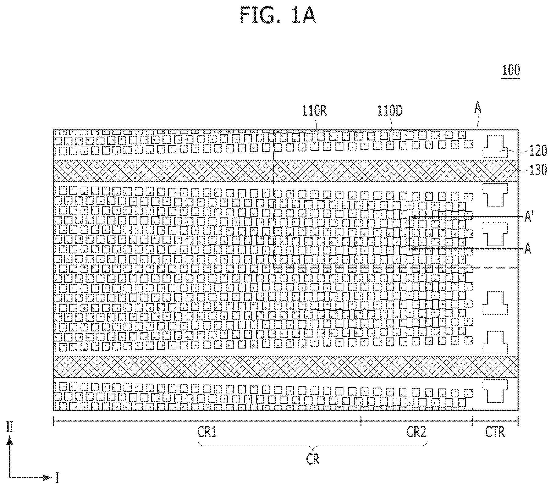
Hereinafter, embodiments according to the technical spirit of the present disclosure are described with reference to the accompanying drawings. Embodiments of the present disclosure may provide a semiconductor device having a stable structure and improved characteristics and a method of manufacturing a semiconductor device. Various embodiments of the present technology can provide a semiconductor device having a stable structure and improved reliability. A to 1 C are diagrams for describing a semiconductor device according to an embodiment of the present disclosure. B may be an enlarged view of A in A . C may be a cross-sectional view of a first channel structure 110 R and a second channel structure 110 D. Referring to A and 1 B , the semiconductor device may include a gate structure 100 , the first channel structures 110 R, the second channel structures 110 D, or slit structures 130 or may include the gate structure 100 , the first channel structures 110 R, the second channel structures 110 D, or the slit structures 130 in combination. The semiconductor device may further include supports 120 . The gate structure 100 may include a cell region CR and a contact region CTR. The cell region CR may include a first region CR 1 and a second region CR 2 . The second region CR 2 may be disposed closer to the contact region CTR than the first region CR 1 . The channel structures 110 R and 110 D may be disposed in the cell region CR. The supports 120 or contact plugs may be disposed in the contact region CTR. In other words, different structures may be disposed in the cell region CR and the contact region CTR, respectively, on the basis of a boundary surface between the cell region CR and the contact region CTR, but the present disclosure is not limited thereto. The supports 120 or the contact plugs may be disposed in the cell region CR, and the channel structures 110 R and 110 D may be disposed in the contact region CTR. The gate structure 100 may include insulating layers 101 and conductive layers 102 that are alternately stacked. In this case, the insulating layers 101 may include an insulating material, such as oxide. The conductive layers 102 may include a conductive material, such as tungsten. The conductive layers 102 may each be a word line or a selection line. The slit structures 130 may be disposed within the gate structure 100 . The slit structures 130 may extend in a first direction I through the gate structure 100 . For example, the slit structures 130 may extend from the cell region CR to the contact region CTR. The slit structures 130 may be disposed in a second direction II that intersects the first direction I by being spaced apart from each other. The slit structures 130 may include an insulating material or a conductive material or may include the insulating material or the conductive material in combination. The first channel structures 110 R may be disposed in the cell region CR of the gate structure 100 . For example, the first channel structures 110 R may be disposed in the first region CR 1 . The second channel structures 110 D may be disposed in the cell region CR of the gate structure 100 , and may be disposed to be more adjacent to the contact region CTR of the gate structure 100 than the first channel structures 110 R. For example, the second channel structures 110 D may be disposed in the second region CR 2 . The first channel structures 110 R may each include a channel layer 110 RA. The first channel structures 110 R may each further include a memory layer 110 RB that surrounds the sidewall of the channel layer 110 RA or an insulating core 110 RC within the channel layer 110 RA or may each further include the memory layer 110 RB or the insulating core 110 RC in combination. The second channel structures 110 D may each include a channel layer 110 DA, a memory layer 110 DB, or an insulating core 110 DC or may each include the channel layer 110 DA, the memory layer 110 DB, or the insulating core 110 DC in combination. Memory cells may be stacked along the channel structures 110 R and 110 D. The second channel structures 110 D may be disposed closer to the contact region CTR than the first channel structures 110 R. A distance between the first channel structures 110 R or the second channel structures 110 D and the slit structure 130 may be increased as the first channel structures 110 R or the second channel structures 110 D become closer to the contact region CTR. For example, in the second direction II, the first channel structures 110 R may be spaced apart from the slit structure 130 by a first distance “d 1 ”. In the second direction II, the second channel structures 110 D may be spaced apart from the slit structure 130 by a second distance “d 2 ”. The first distance “d 1 ” may be substantially the same as or different from the second distance “d 2 ”. For example, the second distance “d 2 ” may be greater than the first distance “d 1 ”. The form of the slit structure 130 may be influenced by a surrounding environment. If the pattern density of the cell region CR and the pattern density of the contact region CTR are different from each other, the slit structure 130 may be deformed at a boundary between the cell region CR and the contact region CTR at which the pattern density is changed. The term “pattern density” may mean a degree of distribution of structures (patterns) located in region. For example, a first pattern density may mean the degree of distribution of the first channel structures 110 R located in the first region CR 1 , and a second pattern density may mean the degree of distribution of the second channel structures 110 D located in the second region CR 2 . The term “degree of distribution” may mean distance between at least two structures (patterns) or may mean average of distances between two or more structures (patterns). The slit structure 130 may be inclined or some region of the slit structure 130 may protrude. Accordingly, in an embodiment, the distance between the channel structures 110 R and 110 D and the slit structure 130 may be adjusted so that the deformation of the slit structure 130 attributable to a change in the surrounding pattern is minimized. In an embodiment, a change in the form of the slit structure 130 in the boundary surface between the cell region CR and the contact region CTR can be prevented or reduced because the distance between the second channel structures 110 D and the slit structure 130 is increased in the second direction II as the second channel structures 110 D become closer to the contact region CTR. For example, if the second distance “d 2 ” is substantially the same as the first distance “d 1 ”, a form of the slit structure 130 may be changed. However, a change in the form of the slit structure 130 can be reduced because the second channel structures 110 D are disposed so that the second distance “d 2 ” is greater than the first distance “d 1 ”. The first channel structures 110 R may be spaced apart from each other at a first interval “r 1 ” in the first direction I, and may be spaced apart from each other at a second interval “r 2 ” in the second direction II. The second channel structures 110 D may be spaced apart from each other at a third interval “r 3 ” in the first direction I, and may be spaced apart from each other at a fourth interval “r 4 ” in the second direction II. The first interval “r 1 ” and the third interval “r 3 ” may be substantially the same or different from each other. The second interval “r 2 ” and the fourth interval “r 4 ” may be substantially the same or different from each other. The number of channel rows of the first channel structures 110 R and the number of channel rows of the second channel structures 110 D may be substantially the same or different from each other. In this case, the channel row may include the channel structures 110 R and 110 D that are arranged in the first direction I. If the second distance “d 2 ” is greater than the first distance “d 1 ”, the interval between the channel rows of the second channel structures 110 D may be reduced. Accordingly, the fourth interval “r 4 ” may be smaller than the second interval “r 2 ”. Furthermore, in order to compensate for a difference between the pattern densities of the first region CR 1 and the second region CR 2 according to a difference between the second interval “r 2 ” and the fourth interval “r 4 ”, the third interval “r 3 ” may be greater than the first interval “r 1 ”. Accordingly, a first diagonal line distance S 1 between the first channel structures 110 R and a second diagonal line distance S 2 between the second channel structures 110 D may be substantially the same. Furthermore, the pattern density of the first channel structures 110 R and the pattern density of the second channel structures 110 D may be maintained to be substantially identical to each other. The channel structures 110 R and 110 D may each be a real channel structure or a dummy channel structure. The real channel structure and the dummy channel structure may have similar structures, but electrical connection states of the real channel structure and the dummy channel structure may be different from each other. The real channel structure may be connected between a source line and a bit line. Memory cells that are stacked along the real channel structure may be real memory cells that store data. The dummy channel structure may have an electrically floated state. Memory cells that are stacked along the dummy channel structure may be dummy memory cells in which data is not stored. In an embodiment, memory cells that are stacked along the dummy channel structure may be dummy memory cells in which data is unable to be stored. For example, the first channel structures 110 R may each be a real channel structure, and the second channel structures 110 D may each be a dummy channel structure. In this case, a distance between the first channel structures 110 R and the slit structure 130 may be substantially the same, but the present disclosure is not limited thereto. The distance between the first channel structures 110 R and the slit structure 130 may be increased as the first channel structures 110 R become closer to the contact region CTR. Furthermore, a distance between the second channel structures 110 D and the slit structure 130 may be increased as the second channel structures 110 D become closer to the contact region CTR. As another example, the first channel structures 110 R and the second channel structures 110 D may each be a dummy channel structure. In this case, a distance between the first channel structures 110 R and the slit structure 130 may be increased as the first channel structures 110 R become closer to the contact region CTR. Furthermore, a distance between the second channel structures 110 D and the slit structure 130 may be increased as the second channel structures 110 D become closer to the contact region CTR. However, the present disclosure is not limited to the examples. The first channel structures 110 R and the second channel structures 110 D may each be a real channel structure. A distance between the first channel structures 110 R and the slit structure 130 may be substantially the same. A distance between the second channel structures 110 D and the slit structure 130 may be increased as the second channel structures 110 D become closer to the contact region CTR. Alternatively, the distance between the first channel structures 110 R and the slit structure 130 may be increased as the first channel structures 110 R becomes closer to the contact region CTR. The distance between the second channel structures 110 D and the slit structure 130 may be increased as the second channel structures 110 D become closer to the contact region CTR. According to an aforementioned structure, the second distance “d 2 ” between the second channel structures 110 D and the slit structure 130 in the second direction II may be increased as the second channel structures 110 D become closer to the contact region CTR. As the second distance “d 2 ” is increased, the fourth interval “r 4 ” between the second channel structures 110 D in the second direction II may be reduced. In order to compensate for the reduction in the distance, the third interval “r 3 ” between the second channel structures 110 D in the first direction I may be increased. Accordingly, in an embodiment, although the second distance “d 2 ” is increased, the pattern density of the second channel structures 110 D can be maintained. Furthermore, in an embodiment, a change in the form of the slit structure 130 at the boundary surface between the cell region CR and the contact region CTR can be prevented or reduced. A and 2 B are diagrams for describing a semiconductor device according to an embodiment of the present disclosure. A may be a plan view of a cell region CR and a contact region CTR. B may be a cross-sectional view of a first channel structure 210 R 1 , a second channel structure 210 D 1 , a third channel structure 210 R 2 , and a fourth channel structure 210 D 2 . Hereinafter, a description of contents that are redundant with aforementioned contents will be omitted. Referring to A and 2 B , the semiconductor device may include a first gate structure 200 A, a second gate structure 200 B, the first channel structures 210 R 1 , the second channel structures 210 D 1 , the third channel structures 210 R 2 , the fourth channel structures 210 D 2 , supports 220 , or slit structures 230 or may include the first gate structure 200 A, the second gate structure 200 B, the first channel structures 210 R 1 , the second channel structures 210 D 1 , the third channel structures 210 R 2 , the fourth channel structures 210 D 2 , the supports 220 , or the slit structures 230 in combination. The first gate structure 200 A and the second gate structure 200 B may each include the cell region CR and the contact region CTR. The cell region CR may include a first region CR 1 and a second region CR 2 . The second region CR 2 may be disposed closer to the contact region CTR than the first region CR 1 . The second gate structure 200 B may be disposed on the first gate structure 200 A. The first gate structure 200 A may include first insulating layers 201 and first conductive layers 202 that are alternately stacked. The second gate structure 200 B may include second insulating layers 203 and second conductive layers 204 that are alternately stacked. The slit structures 230 may be disposed within the first gate structure 200 A and the second gate structure 200 B, and may extend in a first direction I. For example, the slit structures 230 may extend from the cell region CR to the contact region CTR. The first channel structures 210 R 1 and the second channel structures 210 D 1 may be disposed within the first gate structure 200 A. For example, the first channel structures 210 R 1 or the second channel structures 210 D 1 may be disposed in the cell region CR. The first channel structures 210 R 1 may be disposed in the first region CR 1 . The second channel structures 210 D 1 may be disposed in the second region CR 2 . The first channel structures 210 R 1 may each include a first channel layer 210 R 1 A, a first memory layer 210 R 1 B, or a first insulating core 210 R 1 C or may each include the first channel layer 210 R 1 A, the first memory layer 210 R 1 B or the first insulating core 210 R 1 C in combination. The second channel structures 210 D 1 may each include a second channel layer 210 D 1 A, a second memory layer 210 D 1 B, or a second insulating core 210 D 1 C or may each include the second channel layer 210 D 1 A, the second memory layer 210 D 1 B, or the second insulating core 210 D 1 C in combination. The third channel structures 210 R 2 and the fourth channel structures 210 D 2 may be disposed within the second gate structure 200 B. For example, the third channel structures 210 R 2 or the fourth channel structures 210 D 2 may be disposed in the cell region CR. The third channel structures 210 R 2 may be connected to the first channel structures 210 R 1 . The fourth channel structures 210 D 2 may be connected to the second channel structures 210 D 1 . The third channel structures 210 R 2 may each include the third channel layer 210 R 2 A, the third memory layer 210 R 2 B, or the third insulating core 210 R 2 C or may each include the third channel layer 210 R 2 A, the third memory layer 210 R 2 B, or the third insulating core 210 R 2 C in combination. The fourth channel structures 210 D 2 may each include the fourth channel layer 210 D 2 A, the fourth memory layer 210 D 2 B, or the fourth insulating core 210 D 2 C or may each include the fourth channel layer 210 D 2 A, the fourth memory layer 210 D 2 B, or the fourth insulating core 210 D 2 C in combination. The first channel structure 210 R 1 and the third channel structure 210 R 2 may be interconnected and may form one channel structure. For example, a portion that belongs to a channel structure and that is disposed within the first gate structure 200 A may be the first channel structure 210 R 1 . A portion that belongs to the channel structure and that is disposed within the second gate structure 200 B may be the third channel structure 210 R 2 . Memory cells that are stacked along the first channel structure 210 R 1 and memory cells that are stacked along the third channel structure 210 R 2 may constitute one memory string. The second channel structure 210 D 1 and the fourth channel structure 210 D 2 may be interconnected, and may form one channel structure. For example, a portion that belongs to a channel structure and that is disposed within the first gate structure 200 A may be the second channel structure 210 D 1 . A portion that belongs to the channel structure and that is disposed within the second gate structure 200 B may be the fourth channel structure 210 D 2 . Memory cells that are stacked along the second channel structure 210 D 1 and memory cells that are stacked along the fourth channel structure 210 D 2 may constitute one memory string. The distance between the first channel structures 210 R 1 and the slit structure 230 may be substantially the same as the distance between the third channel structures 210 R 2 and the slit structure 230 . For example, in the second direction II, the first channel structures 210 R 1 may be spaced apart from the slit structure 230 by a first distance “d 1 ”, and the third channel structures 210 R 2 may be spaced apart from the slit structure 230 by a third distance “d 3 ”. Accordingly, the third channel structures 210 R 2 and the first channel structures 210 R 1 may be aligned and disposed, but the present disclosure is not limited thereto. The distance between the first channel structures 210 R 1 and the slit structure 230 may be greater than the distance between the third channel structures 210 R 2 and the slit structure 230 . In such a case, the third channel structures 210 R 2 and the first channel structures 210 R 1 may be offset and disposed. The distance between the second channel structures 210 D 1 and the slit structure 230 may be substantially the same as the distance between the fourth channel structures 210 D 2 and the slit structure 230 . For example, in the second direction II, the second channel structures 210 D 1 may be spaced apart from the slit structure 230 by a second distance “d 2 ”, and the fourth channel structures 210 D 2 may be spaced apart from the slit structure 230 by a fourth distance “d 4 ”. Accordingly, the second channel structures 210 D 1 and the fourth channel structures 210 D 2 may be aligned and disposed, but the present disclosure is not limited thereto. The distance between the second channel structures 210 D 1 and the slit structure 230 may be greater than the distance between the fourth channel structures 210 D 2 and the slit structure 230 . For example, in the second direction II, the fourth distance “d 4 ” is smaller than the second distance “d 2 ”. Therefore, the second channel structures 210 D 1 and the fourth channel structures 210 D 2 may be offset and disposed. A distance between the first channel structures 210 R 1 and the slit structure 230 may be increased as the first channel structures 210 R 1 become closer to the contact region CTR. Furthermore, a distance between the second channel structures 210 D 1 and the slit structure 230 may be increased as the second channel structures 210 D 1 become closer to the contact region CTR. A distance between the third channel structures 210 R 2 and the slit structure 230 may be increased as the third channel structures 210 R 2 become closer to the contact region CTR. A distance between the fourth channel structures 210 D 2 and the slit structure 230 may be increased as the fourth channel structures 210 D 2 become closer to the contact region CTR. For example, the third distance “d 3 ” may be substantially the same as or different from the fourth distance “d 4 ”. The fourth distance “d 4 ” may be greater than the third distance “d 3 .” According to an aforementioned structure, the arrangement of the first channel structures 210 R 1 and the second channel structures 210 D 1 that are disposed within the first gate structure 200 A and the arrangement of the third channel structures 210 R 2 and the fourth channel structures 210 D 2 that are disposed within the second gate structure 200 B may be substantially the same. For example, the first channel structures 210 R 1 may be spaced apart from each other at a first interval “r 1 ” in the first direction I, and also the third channel structures 210 R 2 may be spaced apart from each other at the first interval “r 1 ” in the first direction I. The first channel structures 210 R 1 may be spaced apart from each other at a second interval “r 2 ” in the second direction II, and also the third channel structures 210 R 2 may be spaced apart from each other at the second interval “r 2 ” in the second direction II. And, the second channel structures 210 D 1 may be spaced apart from each other at a third interval “r 3 ” in the first direction I, and also the fourth channel structures 210 D 2 may be spaced apart from each other at the third interval “r 3 ” in the first direction I. The second channel structures 210 D 1 may be spaced apart from each other at a fourth interval “r 4 ” in the second direction II, and also the fourth channel structures 210 D 2 may be spaced apart from each other at the fourth interval “r 4 ” in the second direction II. Furthermore, pattern density of the third channel structures 210 R 2 and the pattern density of the fourth channel structures 210 D 2 may be maintained to be substantially identical to each other. The distance between the first channel structures 210 R 1 and the slit structure 230 and the distance between the second channel structures 210 D 1 and the slit structure 230 may be increased as the first channel structures 210 R 1 and the second channel structures 210 D 1 become closer to the contact region CTR. Similarly, in the second gate structure 200 B, the distance between the third channel structures 210 R 2 and the slit structure 230 and the distance between the fourth channel structures 210 D 2 and the slit structure 230 may be increased as the third channel structures 210 R 2 and the fourth channel structures 210 D 2 become closer to the contact region CTR. Accordingly, in an embodiment, a change in the form of the slit structure 230 at a boundary surface between the cell region CR and the contact region CTR can be prevented or reduced. A to 3 D are diagrams for describing a semiconductor device according to an embodiment of the present disclosure. A may be a plan view of the semiconductor device. B may be an enlarged view of B in A . C and 3 D may be cross-sectional views of the first channel structure 210 R 1 , the second channel structure 210 D 1 , the third channel structure 210 R 2 , and the fourth channel structure 210 D 2 . Hereinafter, a description of contents that are redundant with aforementioned contents will be omitted. Referring to A to 3 D , the semiconductor device may include the first gate structure 200 A, the second gate structure 200 B, the first channel structures 210 R 1 , the second channel structures 210 D 1 , the third channel structures 210 R 2 , the fourth channel structures 210 D 2 , the supports 220 , or the slit structures 230 or may include the first gate structure 200 A, the second gate structure 200 B, the first channel structures 210 R 1 , the second channel structures 210 D 1 , the third channel structures 210 R 2 , the fourth channel structures 210 D 2 , the supports 220 , or the slit structures 230 in combination. The third channel structures 210 R 2 and the fourth channel structures 210 D 2 may be disposed in the cell region CR of the second gate structure 200 B. The distance between the third channel structures 210 R 2 and the slit structure 230 and the distance between the fourth channel structures 210 D 2 and the slit structure 230 may be constant. For example, the distance between the channel structures 210 R 2 and 210 D 2 and the slit structure 230 may be constant regardless of the cell region CR or the contact region CTR. For reference, locations, arrangements, and forms of the first gate structure 200 A that is disposed under the second gate structure 200 B and the first channel structures 210 R 1 and the second channel structures 210 D 1 that are disposed in the cell region CR of the first gate structure 200 A may be similar to those that have been described with reference to A and 2 B . The distance between the first channel structures 210 R 1 and the slit structure 230 and the distance between the second channel structures 210 D 1 and the slit structure 230 may be increased as the first channel structures 210 R 1 and the second channel structures 210 D 1 become closer to the contact region CTR. Accordingly, the channel structures 210 R 2 and 210 D 2 of the second gate structure 200 B and the channel structures 210 R 1 and 210 D 1 of the first gate structure 200 A may be offset and disposed. Referring to C , the first channel structures 210 R 1 and the third channel structures 210 R 2 may be offset and disposed, and may be interconnected through overlapped portions of the first channel structures 210 R 1 and the third channel structures 210 R 2 . The second channel structures 210 D 1 and the fourth channel structures 210 D 2 may be offset and disposed, and may be interconnected through overlapped portions of the second channel structures 210 D 1 and the fourth channel structures 210 D 2 . Referring to D , a sacrificial layer 210 S may be disposed within the first gate structure 200 A. The third channel structures 210 R 2 and the fourth channel structures 210 D 2 may be disposed within the second gate structure 200 B. That is, the sacrificial layers 210 S may be disposed within the first gate structure 200 A instead of the first channel structures 210 R 1 and the second channel structures 210 D 1 . The sacrificial layers 210 S may be offset and disposed so that the sacrificial layers 210 S do not overlap the third channel structure 210 R 2 and the fourth channel structure 210 D 2 . The sacrificial layers 210 S may remain without being replaced with the first channel structure 210 R 1 or the second channel structure 210 D 1 in a process of manufacturing the semiconductor device. According to an aforementioned structure, the arrangement of the first channel structures 210 R 1 and the second channel structures 210 D 1 that are disposed within the first gate structure 200 A and the arrangement of the third channel structures 210 R 2 and the fourth channel structures 210 D 2 that are disposed within the second gate structure 200 B may be different from each other. The distance between the channel structures 210 R 1 and 210 D 1 and the slit structure 230 within the first gate structure 200 A may be increased as the channel structures 210 R 1 and 210 D 1 become closer to the contact region CTR. The distance between the channel structures 210 R 2 and 210 D 2 and the slit structure 230 within the second gate structure 200 B may be constant. is a diagram for describing a semiconductor device according to an embodiment of the present disclosure. Hereinafter, a description of contents that are redundant with aforementioned contents will be omitted. Referring to , the semiconductor device may include a gate structure 300 , first channel structures 310 R, second channel structures 310 D, or a slit structure 330 or may include the gate structure 300 , the first channel structures 310 R, the second channel structures 310 D, or the slit structure 330 in combination. The semiconductor device may further include supports 320 or bit lines 340 or may further include the supports 320 or the bit lines 340 in combination. The gate structure 300 , the channel structures 310 R and 310 D, and the slit structure 330 may be the gate structure 100 , the channel structures 110 R and 110 D, and the slit structure 130 , respectively, which have been described with reference to A to 1 C . The channel structures 310 R and 310 D may be disposed in a cell region CR of the gate structure 300 . For example, the first channel structures 310 R may be disposed in a first region CR 1 of the cell region CR. The second channel structures 310 D may be disposed in a second region CR 2 of the cell region CR. The channel structures 310 R and 310 D may each be a real channel structure or a dummy channel structure. For example, the first channel structures 310 R may each be a real channel structure, and the second channel structures 310 D may each be a dummy channel structure. In this case, a distance between the first channel structures 310 R and the slit structure 330 may be increased as the first channel structures 310 R become closer to the contact region CTR. A distance between the second channel structures 310 D and the slit structure 330 may be increased as the second channel structures 310 D become closer to the contact region CTR. The bit lines 340 may be disposed in the cell region CR of the gate structure 300 . Furthermore, the bit lines 340 may be disposed on a real channel structure, and may be connected to the real channel structures. For example, the bit lines 340 may be connected to the first channel structures 310 R. The bit lines 340 may extend in a second direction II that intersects a first direction I, and may be connected to the first channel structures 310 R. The bit lines 340 may be disposed in the first direction I in a way to be spaced apart from each other. An interval between the bit lines 340 may be increased as the bit lines 340 become closer to a contact region CTR. The bit lines 340 may include first bit lines 340 A or second bit lines 340 B. The second bit lines 340 B may be disposed closer to the contact region CTR than the first bit lines 340 A. The first bit lines 340 A may be spaced apart from each other at a first interval P 1 in the first direction I. The second bit lines 340 B may be spaced apart from each other at a second interval P 2 in the first direction I. The first interval P 1 and the second interval P 2 may be substantially the same or different from each other. For example, the second interval P 2 may be greater than the first interval P 1 . For reference, both the first channel structures 310 R and the second channel structures 310 D may each be a real channel structure. In this case, an interval between the bit lines 340 that are connected to the channel structures 310 R and 310 D may be increased as the bit lines 340 become closer to the contact region CTR. According to an aforementioned structure, the intervals P 1 and P 2 between the bit lines 340 that are connected to the channel structures 310 R and 310 D may also be changed depending on distances between the channel structures 310 R and 310 D and the slit structure 330 . The intervals P 1 and P 2 may be increased as the bit lines 340 become closer to the contact region CTR. A to 5 D are diagrams for describing a method of manufacturing a semiconductor device according to an embodiment of the present disclosure. Hereinafter, a description of contents that are redundant with aforementioned contents will be omitted. Referring to A , a stack 400 may be formed. The stack 400 may include first material layers and second material layers that are alternately stacked. In this case, the first material layers may include an insulating material, such as oxide. The second material layers may include a sacrificial material, such as nitride. Alternatively, the first material layers may include an insulating material, such as oxide. The second material layers may include a conductive material, such as tungsten. The stack 400 may include a cell region CR and a contact region CTR. The cell region CR may include a first region CR 1 and a second region CR 2 . The second region CR 2 may be disposed closer to the contact region CTR than the first region CR 1 . Referring to B and 5 C , a mask M may be formed on the stack 400 . In this case, the mask M may include a hard mask or a photoresist or may include the hard mask or the photoresist in combination. Next, first openings OP 1 , second openings OP 2 , or third openings OP 3 may be formed within the stack 400 or the first openings OP 1 , the second openings OP 2 , or the third openings OP 3 may be formed in combination within the stack 400 , by using the mask M as an etch barrier. The first openings OP 1 and the second openings OP 2 may be formed in the cell region CR. The third openings OP 3 may be formed in the contact region CTR. The first openings OP 1 may be formed in the first region CR 1 . The second openings OP 2 may be formed in the second region CR 2 . The first openings OP 1 , the second openings OP 2 , and the third openings OP 3 may be simultaneously formed, but the present disclosure is not limited thereto. After the first openings OP 1 and the second openings OP 2 are formed, the third openings OP 3 may be formed. The words “simultaneous” and “simultaneously” as used herein with respect to processes mean that the processes take place on overlapping intervals of time. For example, if a first process takes place over a first interval of time and a second process takes place simultaneously over a second interval of time, then the first and second intervals at least partially overlap each other such that there exists a time at which the first and second processes are both taking place. An interval between the first openings OP 1 or an interval between the second openings OP 2 may be different depending on a distance from the contact region CTR. For example, an interval between the first openings OP 1 in a first direction I and an interval between the second openings OP 2 in the first direction I may be increased as the first openings OP 1 and the second openings OP 2 become closer to the contact region CTR. Furthermore, an interval between the first openings OP 1 in a second direction II that intersects the first direction I and an interval between the second openings OP 2 in the second direction II may be reduced as the first openings OP 1 and the second openings OP 2 become closer to the contact region CTR. The first openings OP 1 or the second openings OP 2 may be formed by considering a region OP 4 A in which a fourth opening will be formed. The second openings OP 2 may be disposed closer to the contact region CTR than the first openings OP 1 . The openings OP 1 and OP 2 may be formed so that distances between the openings OP 1 and OP 2 and the region OP 4 A in which the fourth opening will be formed are increased as the openings OP 1 and OP 2 become closer to the contact region CTR. For example, in the second direction II, the first openings OP 1 may be formed to be spaced apart from the region OP 4 A in which the fourth opening will be formed by a first distance “d 1 ”. In the second direction II, the second openings OP 2 may be formed to be spaced apart from the region OP 4 A in which the fourth opening will be formed by a second distance “d 2 ”. The first distance “d 1 ” may be substantially the same as or different from the second distance “d 2 ”. For example, the second distance “d 2 ” may be greater than the first distance “d 1 ”. The first openings OP 1 may be spaced apart from each other at a first interval “r 1 ” in the first direction I, and may be spaced apart from each other at a second interval “r 2 ” in the second direction II. The second openings OP 2 may be spaced apart from each other at a third interval “r 3 ” in the first direction I, and may be spaced apart from each other at a fourth interval “r 4 ” in the second direction II. The first interval “r 1 ” and the third interval “r 3 ” may be substantially the same or different from each other. The second interval “r 2 ” and the fourth interval “r 4 ” may be substantially the same or different from each other. The number of opening rows of the first openings OP 1 and the number of opening rows of the second openings OP 2 may be substantially the same or different from each other. In this case, the opening row may include the openings OP 1 or OP 2 that are arranged in the first direction I. If the second distance “d 2 ” is greater than the first distance “d 1 ”, an interval between the opening rows of the second openings OP 2 may be reduced. Accordingly, the fourth interval “r 4 ” may be smaller than the second interval “r 2 ”. Furthermore, in order to compensate for a difference between the pattern density of the first openings OP 1 and the pattern density of the second openings OP 2 according to a difference between the second interval “r 2 ” and the fourth interval “r 4 ”, the third interval “r 3 ” may be greater than the first interval “r 1 ”. Accordingly, a first diagonal line distance S 1 between the first openings OP 1 and a second diagonal line distance S 2 between the second openings OP 2 may be substantially the same. Furthermore, the pattern densities of the first openings OP 1 and the second openings OP 2 may be maintained substantially identically. Referring to D , first channel structures 410 R may be formed within the first openings OP 1 , respectively. Accordingly, the first channel structures 410 R that extend through the stack 400 may be formed. Second channel structures 410 D may be formed within the second openings OP 2 , respectively. Accordingly, the second channel structures 410 D that extend through the stack 400 may be formed. The second channel structures 410 D may be formed simultaneously with the first channel structures 410 R, but the present disclosure is not limited thereto. After the first channel structures 410 R are formed, the second channel structures 410 D may be formed. The channel structures 410 R and 410 D may be similar to the channel structures 110 R and 110 D, respectively, which have been described with reference to A to 1 C . The channel structures 410 R and 410 D may each include a channel layer, a memory layer, or an insulating core or may each include the channel layer, the memory layer, or the insulating core in combination. The channel structures 410 R and 410 D may each be a real channel structure or a dummy channel structure. The real channel structure and the dummy channel structure may have similar structures. Electrical connection states of the real channel structure and the dummy channel structure may be different from each other. For example, the first channel structures 410 R may each be a real channel structure. The second channel structures 410 D may each be a dummy channel structure. As another example, the first channel structures 410 R and the second channel structures 410 D may each be a dummy channel structure. Supports 420 may be formed within the third openings OP 3 , respectively. The supports 420 may be formed in the contact region CTR. The supports 420 may be simultaneously formed when the channel structures 410 R and 410 D are formed, but the present disclosure is not limited thereto. After the channel structures 410 R and 410 D are formed, the supports 420 may be formed. Next, a fourth opening OP 4 that extends in the first direction I may be formed within the stack 400 . In this case, the fourth opening OP 4 may be a slit. The fourth opening OP 4 may be formed between the first channel structures 410 R, between the second channel structures 410 D, or between the supports 420 the first channel structures 410 R, the second channel structures 410 D, or the supports 420 being spaced apart from each other in the second direction II. A form of the fourth opening OP 4 may be influenced by a surrounding environment. If the pattern density of the cell region CR and the pattern density of the contact region CTR are different from each other, a form of the fourth opening OP 4 may be deformed at a boundary between the cell region CR and the contact region CTR at which the pattern density is changed. For example, the fourth opening OP 4 may have an inclined form, or some region of the fourth opening OP 4 may protrude. In an embodiment, the fourth opening OP 4 can be prevented from being inclined or deformed or the inclination or deformation of the fourth opening OP 4 can be reduced because the openings OP 1 and OP 2 are formed by adjusting the distance between the fourth opening OP 4 and the openings OP 1 and OP 2 so that the deformation of the fourth opening OP 4 is minimized. Next, a slit structure 430 may be formed within the fourth opening OP 4 . The relation between the intervals r 1 , r 2 , and S 1 among the first openings OP 1 , the relation between the intervals r 3 , r 4 , and S 2 among the second openings OP 2 , and the relation between the distances d 1 and d 2 between the openings OP 1 and OP 2 and the fourth opening OP 4 may also be identically applied to a relation between the channel structures 410 R and 410 D and a relation between the channel structures 410 R and 410 D and the slit structure 430 . For reference, the gate structure may be formed within the stack 400 by replacing sacrificial materials with conductive layers. Furthermore, when the stack 400 is formed, if insulating layers and conductive layers are alternately stacked, a process of replacing the sacrificial materials may be omitted. Alternatively, a process for reducing resistance of the conductive layers, such as a silicidation process, may also be performed. In this case, the stack 400 may be a gate structure. Furthermore, bit lines that are connected to real channel structures may be formed. For example, if the first channel structures 410 R are real channel structures and the second channel structures 410 D are dummy channel structures, bit lines that are connected to the first channel structures 410 R may be formed. In this case, if a distance between the first channel structures 410 R and the slit structure 430 is increased as the first channel structures 410 R become closer to the contact region CTR, an interval between the bit lines may be increased. According to an aforementioned process, locations of the openings OP 1 and OP 2 may be determined by considering a location at which the fourth opening OP 4 will be formed. For example, the openings OP 1 and OP 2 may be formed so that the openings OP 1 and OP 2 become distant from locations at which the fourth opening OP 4 will be formed as the openings OP 1 and OP 2 become closer to the contact region CTR. Accordingly, in an embodiment, a change in the form of the fourth opening OP 4 can be prevented or minimized. A to 6 C are diagrams for describing a method of manufacturing a semiconductor device according to an embodiment of the present disclosure. Hereinafter, a description of contents that are redundant with aforementioned contents will be omitted. Referring to A , dummy plugs 550 may be formed within a first stack 500 A. First, fifth openings OP 5 may be formed within the first stack 500 A. In this case, the fifth openings OP 5 may each be a dummy opening. The fifth openings OP 5 may be formed when first openings OP 1 and second openings OP 2 are formed. The fifth openings OP 5 may be formed in a location at which a fourth opening OP 4 will be formed. In other words, a dummy opening may be formed at a location at which a slit will be formed. The first openings OP 1 and the second openings OP 2 may be the same as the first openings OP 1 and the second openings OP 2 that have been described with reference to B to 5 D . The first openings OP 1 and the second openings OP 2 may be formed by considering the location at which the fourth opening OP 4 will be formed. For example, the openings OP 1 and OP 2 may be formed so that the openings OP 1 and OP 2 become distant from the location at which the fourth opening OP 4 will be formed as the openings OP 1 and OP 2 become closer to the contact region CTR. Next, the dummy plugs 550 may be formed within the fifth openings OP 5 , respectively. The dummy plugs 550 may be formed when sacrificial layers 510 RS and 510 DS are formed within the openings OP 1 and OP 2 , respectively. The sacrificial layers 510 RS and 510 DS may include a material that has high etch selectivity to the stack. For example, the sacrificial layers 510 RS and 510 DS may include a conductive material, such as tungsten. The dummy plugs 550 may be formed of the same material as the sacrificial layers 510 RS and 510 DS. For example, the dummy plugs 550 may include a conductive material, such as tungsten. Referring to B and 6 C , a second stack 500 B may be formed on the first stack 500 A. Next, sixth openings OP 6 that are connected to the first openings OP 1 may be formed within the second stack 500 B. Seventh openings OP 7 that are connected to the second openings OP 2 may be formed within the second stack 500 B. For example, the openings OP 6 and OP 7 that expose the channel structures 510 R 1 and 510 D 1 , respectively, may be formed. The openings OP 6 and OP 7 may be formed by considering the location at which the fourth opening OP 4 will be formed. For example, the openings OP 6 and OP 7 may be formed so that the openings OP 6 and OP 7 become distant from the location at which the fourth opening OP 4 will be formed as the openings OP 6 and OP 7 become closer to the contact region CTR. For reference, although not illustrated in these drawings, the second stack 500 B may be formed so that a distance between the fourth opening OP 4 and the openings OP 6 and OP 7 is constant. Next, the first openings OP 1 may be re-opened by removing the sacrificial layers 510 RS within the first openings OP 1 through the sixth openings OP 6 . The second openings OP 2 may be re-opened by removing the sacrificial layers 510 DS within the second openings OP 2 through the seventh openings OP 7 . Next, channel structures 510 R 1 , 510 R 2 , 510 D 1 , and 510 D 2 may be formed within the openings OP 1 , OP 6 , OP 2 , and OP 7 , respectively. For example, the first channel structures 510 R 1 and the third channel structures 510 R 2 may be formed within the sixth openings OP 6 and the first openings OP 1 , respectively. The second channel structures 510 D 1 and the fourth channel structures 510 D 2 may be formed within the seventh openings OP 7 and the second openings OP 2 . In this case, referring back to B , the first channel structures 510 R 1 and the third channel structures 510 R 2 may be aligned and connected, and the second channel structures 510 D 1 and the fourth channel structures 510 D 2 may be aligned and connected. For reference, the channel structures 510 R 1 , 510 R 2 , 510 D 1 , and 510 D 2 may be offset and disposed. For example, referring back to C , the first channel structures 510 R 1 and the third channel structures 510 R 2 may be offset and connected. Referring back to D , that is, the sacrificial layers 510 RS and 510 DS may be disposed within the first stack 500 A instead of the first channel structures 510 R 1 and the second channel structures 510 D 1 . The sacrificial layers 510 RS and 510 DS may be offset and disposed so that the sacrificial layers 510 RS and 510 DS do not overlap the third channel structure 510 R 2 and the fourth channel structure 510 D 2 . The sacrificial layers 510 RS and 510 DS may remain without being replaced with the first channel structure 510 R 1 or the second channel structure 510 D 2 in a process of manufacturing the semiconductor device. Next, the fourth opening OP 4 may be formed. When the fourth opening OP 4 is formed, charges may be discharged through the dummy plug 550 . For example, charges that have been accumulated within the channel structures 510 R 1 , 510 R 2 , 510 D 1 , and 510 D 2 may be discharged through the dummy plug 550 . The dummy plug 550 may be removed in a process of forming the fourth opening OP 4 . Next, a slit structure 530 may be formed within the fourth opening OP 4 . According to an aforementioned process, the dummy plug 550 may be formed within the first stack 500 A before the second stack 500 B is formed. Accordingly, in a process of forming the fourth opening OP 4 , charges that have been accumulated within the channel structures 510 R 1 , 510 R 2 , 510 D 1 , and 510 D 2 can be discharged through the dummy plug 550 . In an embodiment, the deformation of the fourth opening OP 4 attributable to the charges can be prevented or minimized. Although embodiments according to the technical spirit of the present disclosure have been described above with reference to the accompanying drawings, the embodiments have been provided to merely describe embodiments according to the concept of the present disclosure, and the present disclosure is not limited to the embodiments. A person having ordinary knowledge in the art to which the present disclosure pertains may substitute, modify, and change the embodiments in various ways without departing from the technical spirit of the present disclosure written in the claims. Such substitutions, modifications, and changes may be said to belong to the scope of the present disclosure.
Figures (15)
Citations
This patent cites (42)
- US9786673
- US9929174
- US10727245
- US10825934
- US11145594
- US11991880
- US2016/0086969
- US2017/0025434
- US2018/0019257
- US2018/0130814
- US2019/0081064
- US2019/0172794
- US2019/0280004
- US2020/0083246
- US2020/0119031
- US2020/0135753
- US2020/0152654
- US2020/0295027
- US2020/0303396
- US2021/0167076
- US2021/0296345
- US2021/0305271
- US2021/0305273
- US2022/0093756
- US2022/0285389
- US2022/0336437
- US2022/0406805
- US2023/0085996
- US2023/0165000
- US2023/0301098
- US2024/0170389
- US110197830
- US110767657
- US112420724
- US112652628
- US114388530
- US114551454
- US115472618
- US20150033932
- US1020170038513
- US20200032595
- US20200038138