Abstract
It is aimed to provide a card edge connector capable of improving electrical conduction between a terminal and a board. A card edge connector ( 1 ) is provided with a housing ( 12 ) and a terminal fitting ( 13 ) including a base portion ( 13 A) to be fixed to the housing ( 12 ), a contact portion ( 13 D) to be brought into electrical contact with a circuit board ( 62 ) assembled with the housing ( 12 ) and a spring portion ( 13 C) provided between the base portion ( 13 A) and the contact portion ( 13 D) for displaceably supporting the contact portion ( 13 D).
Claims (9)
1 . A card edge connector, comprising: a housing; and a terminal fitting including a base portion to be fixed to the housing, a contact portion to be brought into electrical contact with a board assembled with the housing and a spring portion provided between the base portion and the contact portion for displaceably supporting the contact portion, the spring portion is accommodated in a box portion, and the box portion is inserted into a cavity of the housing.
Show 8 dependent claims
2 . The card edge connector of claim 1 , comprising a box portion for accommodating the spring portion.
3 . The card edge connector of claim 2 , wherein: the box portion is coupled to the base portion via the spring portion, and a gap is provided between the box portion and the base portion.
4 . The card edge connector of claim 3 , wherein the gap is present in a direction orthogonal to a tolerance absorbing direction by the spring portion.
5 . The card edge connector of claim 3 , wherein the gap is present in a direction parallel to the tolerance absorbing direction by the spring portion.
6 . The card edge connector of claim 2 , comprising a locking portion connected to the contact portion and the spring portion, the locking portion locking the box portion.
7 . The card edge connector of claim 1 , wherein a plate thickness direction of the base portion is orthogonal to a tolerance absorbing direction by the spring portion.
8 . The card edge connector of claim 1 , wherein the spring portion includes an S-shaped portion.
9 . The card edge connector of claim 1 , wherein: the contact portion includes a resilient contact portion projecting in a direction orthogonal to an assembling direction of the board with the housing, the resilient contact portion resiliently contacting the board, and the spring portion and the resilient contact portion are arranged in the same direction as the assembling direction.
Full Description
Show full text →
CROSS REFERENCE TO RELATED APPLICATIONS
This application is a national phase of PCT application No. PCT/JP2022/007443, filed on 24 Feb. 2022, which claims priority from Japanese patent application No. 2021-043092, filed on 17 Mar. 2021, all of which are incorporated herein by reference.
TECHNICAL FIELD
The present disclosure relates to a card edge connector.
BACKGROUND
Patent Document 1 discloses an electrical connector in which a connector housing provided with a plurality of connector terminals is connected to a board-side connector provided on a circuit board. This electrical connector is configured to sandwich the circuit board by the plurality of connector terminals.
PRIOR ART
DOCUMENT Patent Document Patent Document 1: JP 2013-171690 A
SUMMARY OF THE INVENTION
Problems to be Solved Generally, the thickness and outer shape of a circuit board easily vary. Thus, if the thickness or outer shape of the circuit board varies in the electrical connector of Patent Document 1, there is a concern that contact pressures of the connector terminals and the circuit board vary. A card edge connector of the present disclosure was completed on the basis of the above situation and aims to provide a card edge connector capable of improving electrical conduction between a terminal and a board. Means to Solve the Problem The present disclosure is directed to a card edge connector with a housing and a terminal fitting including a base portion to be fixed to the housing, a contact portion to be brought into electrical contact with a board assembled with the housing and a spring portion provided between the base portion and the contact portion for displaceably supporting the contact portion. Effect of the Invention According to the present disclosure, electrical conduction between a terminal and a board can be improved.
BRIEF DESCRIPTION OF THE DRAWINGS
is a perspective view of a card edge connector according to an embodiment. is a plan view of the card edge connector. is a section along A-A in . is a section along B-B in . is a section along C-C in . is a section along D-D in . is a section along B-B in showing a state assembled with a circuit board. is a perspective view showing a shaft portion in another embodiment.
DETAILED DESCRIPTION
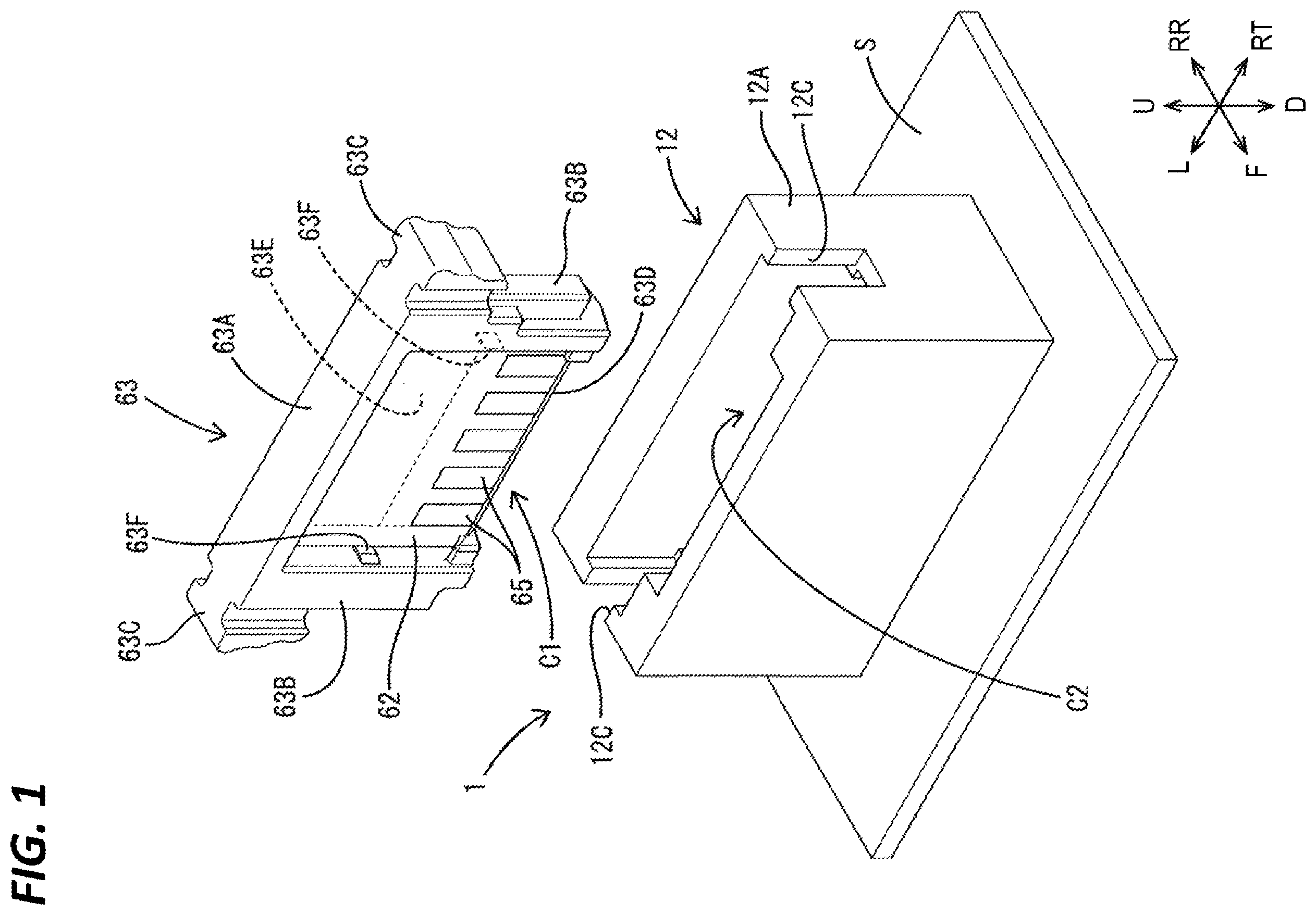
TO EXECUTE THE INVENTION Description of Embodiments of Present Disclosure First, embodiments of the present disclosure are listed and described. (1) The card edge connector of the present disclosure is provided with a housing and a terminal fitting including a base portion to be fixed to the housing, a contact portion to be brought into electrical contact with a board assembled with the housing and a spring portion provided between the base portion and the contact portion for displaceably supporting the contact portion. According to this configuration, since the position of the contact portion is made displaceable by the spring portion, the position of the contact portion is easily adapted to a variation of the board. (2) Preferably, the card edge connector of the present disclosure is provided with a box portion for accommodating the spring portion. According to this configuration, the spring portion can be protected by the box portion. (3) Preferably, the box portion of the card edge connector of the present disclosure is coupled to the base portion via the spring portion and a gap is provided between the box portion and the base portion. According to this configuration, the box portion coupled to the base portion via the spring portion can be displaced without being rubbed against the base portion. (4) Preferably, the gap of the card edge connector of the present disclosure is present in a direction orthogonal to a tolerance absorbing direction by the spring portion. According to this configuration, the box portion and the base portion can be prevented from being rubbed against each other in assembling the board with the housing. (5) Preferably, the gap of the card edge connector of the present disclosure is present in a direction parallel to the tolerance absorbing direction by the spring portion. According to this configuration, since the box portion can also be displaced together with the contact portion, the interference of the box portion and the base portion can be made difficult while the spring portion is protected by the box portion. (6) Preferably, the card edge connector of the present disclosure is provided with a locking portion connected to the contact portion and the spring portion, the locking portion locking the box portion. According to this configuration, since the locking portion locks the box portion, the influence of the spring portion on the movement of the resilient contact portion can be suppressed in assembling the board with the housing. (7) Preferably, a plate thickness direction of the base portion of the card edge connector of the present disclosure is orthogonal to a tolerance absorbing direction by the spring portion. According to this configuration, even if the position of the board with respect to the housing is shifted in the tolerance absorbing direction and the box portion and the contact portion are shifted in the tolerance absorbing direction, the base portion is hardly deformed or deflected. (8) Preferably, the spring portion of the card edge connector of the present disclosure includes an S-shaped portion. According to this configuration, a configuration for displaceably supporting the contact portion can be provided in a smaller region. (9) Preferably, the contact portion of the card edge connector of the present disclosure includes a resilient contact portion projecting in a direction orthogonal to an assembling direction of the board with the housing, the resilient contact portion resiliently contacting the board, and the spring portion and the resilient contact portion are arranged in the same direction as the assembling direction. According to this configuration, a space formed by the resilient contact portion projecting in the direction orthogonal to the assembling direction of the board can be effectively utilized as an accommodation space for the spring portion. DETAILS OF EMBODIMENTS OF PRESENT DISCLOSURE Embodiment Hereinafter, one specific embodiment of the present disclosure is described below with reference to to 7 . Note that, in the following description, an upper side and a lower side in are defined as a left side and a right side concerning a lateral direction. A left side and a right side in are defined as a front side and a rear side concerning a front-rear direction. A frontal side and a back side in are defined as an upper side and a lower side concerning a vertical direction. In a card edge connector 1 according to the embodiment, a circuit board 62 , which is a board, can be fit to terminal fittings 13 provided in a housing 12 . As shown in , the card edge connector 1 is provided with the housing 12 and a plurality of the terminal fittings 13 . [Circuit Board] As shown in , the circuit board 62 has a flat plate shape. Electronic components and the like are mounted on a surface of the circuit board 62 . A plurality of electrically conductive portions 65 are provided side by side in the lateral direction on the surface of the circuit board 62 . The respective electrically conductive portions 65 are arranged at positions corresponding to the plurality of terminal fittings 13 fixed in the housing 12 . [Circuit Board Holding Member] A circuit board holding member 63 is made of synthetic resin. The circuit board holding member 63 includes a basis portion 63 A, a pair of side wall portions 63 B, a pair of grip portions 63 C, an edge portion 63 D, a butting portion 63 E and the like. The basis portion 63 A is formed to extend in the lateral direction. The pair of side wall portions 63 B are formed to extend downward respectively from both end parts in the lateral direction of the basis portion 63 A. The pair of grip portions 63 C are upper end parts of the respective side wall portions 63 B and extend in separating directions from the basis portion 63 A toward both sides in the lateral direction. The edge portion 63 D is provided to connect lower end parts of the pair of side wall portions 63 B and extend in the lateral direction. The butting portion 63 E has a substantially flat plate shape, and is coupled to rear sides of the basis portion 63 A and the respective side wall portions 63 B with a plate thickness direction oriented in the front-rear direction. The circuit board holding member 63 is formed with an accommodation space C 1 for accommodating the circuit board 62 in a region surrounded by the basis portion 63 A, the pair of side wall portions 63 B and the edge portion 63 D. If the circuit board 62 is accommodated into the accommodation space C 1 , the circuit board 62 is held accommodated in the accommodation space C 1 by locking portions 63 F provided on the respective side wall portions 63 B. The edge portion 63 D is arranged to cover the lower end surface of the circuit board 62 from below. The edge portion 63 D is formed with inclined surfaces 63 G to reduce a dimension in the front-rear direction from the lower end surface of the circuit board 62 toward a lower side (see ). [Housing] The housing 12 is made of synthetic resin. As shown in , 3 and 4 , the housing 12 includes a flat plate-like base wall portion 12 A and a peripheral wall portion 12 B continuous around the base wall portion 12 A and extending upward. A plurality of cavities 15 for respectively accommodating the plurality of terminal fittings 13 are formed to penetrate through the base wall portion 12 A in the vertical direction. The plurality of cavities 15 are arranged in a row in the lateral direction. The housing 12 is configured such that the base wall portion 12 A can be coupled to a base board S along the upper surface of the base board S. A pair of slits 15 A are formed in each cavity 15 . The pair of slits 15 A are formed to be recessed in directions separating from each other in front and rear surfaces constituting each cavity 15 . Retaining portions 15 B for restricting the terminal fitting 13 inserted into the cavity 15 from coming out upward are formed on upper sides of the pair of slits 15 A (see ). A pair of the restricting portions 15 B project in directions toward each other on facing inner surfaces of the pair of slits 15 A. An upper part of the peripheral wall portion 12 B is cut to be recessed downward, thereby forming a pair of grooves 12 C (see ). These grooves 12 C are formed side by side with both sides in the lateral direction of the plurality of cavities 15 arranged in a row. The pair of grip portions 63 C of the circuit board holding member 63 are inserted into these grooves 12 C (see ). The housing 12 is formed with an insertion space C 2 , into which the circuit board 62 held in the circuit board holding member 63 is inserted, in a region surrounded by the base wall portion 12 A and the peripheral wall portion 12 B (see ). [Terminal Fitting] The terminal fitting 13 is formed, such as by bending an electrically conductive metal plate. As shown in , the terminal fitting 13 includes a base portion 13 A, a shaft portion 13 B, a spring portion 13 C, a contact portion 13 D, a box portion 13 E and the like. The base portion 13 A has a flat plate shape and is arranged with a plate thickness direction oriented in the lateral direction. An extending portion 13 H extending upward is provided in a central part in the front-rear direction of the base portion 13 A. A rear end part of the extending portion 13 H is bent to extend rightward (see ). A pair of projecting portions 13 F projecting in directions separating from each other along the front-rear direction are provided on lower sides of both end parts in the front-rear direction of the base portion 13 A. The base portion 13 A is fixed to the housing 12 by inserting the both end parts in the front-rear direction thereof into the pair of slits 15 A formed in the cavity 15 of the housing 12 . The shaft portion 13 B extends downward from a central part in the front-rear direction of the lower end of the base portion 13 A. The shaft portion 13 B is formed by being wound into a roll (see ). In this way, one surface of the metal plate is exposed and the other surface is not exposed on the outer peripheral surface of the shaft portion 13 B. The outer peripheral surface of the shaft portion 13 B is constituted by a substantially smooth curved surface. The shaft portion 13 B is inserted into a through hole H formed in the base board S and fixed to the base board S by soldering. Since the outer peripheral surface of the shaft portion 13 B is constituted by the substantially smooth curved surface, solder easily adheres. That is, the outer peripheral surface of the shaft portion 13 B is good in solder wettability. The spring portion 13 C includes an S-shaped portion 13 G having an S shape when viewed from left or right. One end part of the S-shaped portion 13 G is coupled to the extending portion 13 H of the base portion 13 A. The other end part of the S-shaped portion 13 G is located forward of the one end part. One end side of the S-shaped portion 13 G is curved into a U shape to bulge upward. The other end side of the S-shaped portion 13 G is curved into a U shape to bulge downward. These U-shaped parts of the S-shaped portion 13 G can be resiliently changed in the front-rear direction. A coupling portion 13 J extending upward with a plate thickness direction oriented in the front-rear direction is provided on the other end side of the S-shaped portion 13 G. The other end side of the S-shaped portion 13 G can swing in the front-rear direction. That is, a tolerance can be absorbed in the front-rear direction by the spring portion 13 C, and the front-rear direction is a tolerance absorbing direction T. The tolerance absorbing direction T is a direction orthogonal to the plate thickness direction of the base portion 13 A (lateral direction) (see ). The other end side of the spring portion 13 C can swing also in the lateral direction. The contact portion 13 D includes a resilient contact portion 13 K coupled to the upper end of the coupling portion 13 J and extending obliquely to an upper-rear side and a catching portion 13 L coupled to the upper end of the resilient contact portion 13 K and extending oblique to an upper-front side. That is, the contact portion 13 D is coupled to the base portion 13 A via the coupling portion 13 J and the spring portion 13 C. Further, the spring portion 13 C is provided between the base portion 13 A and the contact portion 13 D and displaceably supports the contact portion 13 D by being resiliently deformed. The resilient contact portion 13 K of the contact portion 13 D projects while having a width in a direction orthogonal to an assembling direction K of the circuit board 62 with the housing 12 . The resilient contact portion 13 K of the contact portion 13 D electrically contacts the electrically conductive portion 65 of the circuit board 62 assembled with the housing 12 (see ). The spring portion 13 C and the resilient contact portion 13 K are arranged in the same direction as the assembling direction K. The box portion 13 E has a box shape. The box portion 13 E includes a basis portion 13 U, a box body portion 13 M and a tubular portion 13 N. The basis portion 13 U has a rectangular parallelepiped tubular shape long in the front-rear direction in a plan view (see ). The basis portion 13 U is arranged to cover the extending portion 13 H of the base portion 13 A in the front-rear direction and lateral direction. The basis portion 13 U of the box portion 13 E accommodates the spring portion 13 C. The basis portion 13 U is coupled to the coupling portion 13 J (see ). That is, the box portion 13 E is coupled to the base portion 13 A via the coupling portion 13 J and the spring portion 13 C. The box body portion 13 M extends upward from the upper end of a front side of the basis portion 13 U. The box body portion 13 M is formed with an opening 13 P open rearward. An upper end part of the box body portion 13 M is formed with a first inclined portion 13 Q extending obliquely to a rear-lower side. The first inclined portion 13 Q is arranged to cover a tip part of the catching portion 13 L of the contact portion 13 D from behind (see ). The coupling portion 13 J is in surface contact with inner surfaces of a front wall of the basis portion 13 U and a front wall of the box body portion 13 M (see ). Further, a locking portion 13 R projecting rightward is provided on the right end of the coupling portion 13 J (see ). The locking portion 13 R is connected to the contact portion 13 D and the spring portion 13 C via the coupling portion 13 J. The locking portion 13 R is inserted into an insertion hole 13 S formed in the basis portion 13 U for locking (see ). In this way, even if an external force is applied to the box portion 13 E, relative positions of the box portion 13 E and the contact portion 13 D are hardly shifted. The box portion 13 E and the contact portion 13 D are both coupled to the base portion 13 A via the coupling portion 13 J and the spring portion 13 C. Thus, the box portion 13 E and the contact portion 13 D can integrally swing with respect to the base portion 13 A. The tubular portion 13 N extends upward from the upper end of a rear side of the basis portion 13 U while having a tubular shape. The tubular portion 13 N is arranged behind and adjacent to the opening 13 P of the box body portion 13 and along the box body portion 13 M. A second inclined portion 13 T extending obliquely to a front-lower side is formed on an upper end part of the tubular portion 13 N. An insertion space C 3 , into which the circuit board 62 is inserted, is formed between the opening 13 P of the box body portion 13 M and the tubular portion 13 N. The resilient contact portion 13 K and the catching portion 13 L project rearward via the opening 13 P of the box body portion 13 M. That is, the resilient contact portion 13 K is facing the insertion space C 3 , into which the circuit board 62 is inserted. A width in the front-rear direction of the box body portion 13 M is larger than that of the tubular portion 13 N. That is, the insertion space C 3 is formed at a position close to the rear side of the box portion 13 E. As shown in , gaps A and B are provided between the basis portion 13 U of the box portion 13 E and the base portion 13 A. The gaps A are present in a direction parallel to the tolerance absorbing direction T by the spring portion 13 C. The gaps B are present in a direction orthogonal to the tolerance absorbing direction T by the spring portion 13 C. The box portion 13 E of the terminal fitting 13 is inserted into each cavity 15 of the housing 12 from below, and the both end parts in the front-rear direction of the base portion 13 A are inserted into the pair of slits 15 A. Since a dimension between the tips of the pair of projecting portions 13 F of the base portion 13 A is larger than a dimension between the restricting portions 15 B of the slits 15 A, the terminal fitting 13 is restricted from coming up upward (see ). [Assembling of Card Edge Connector with Circuit Board] The circuit board 62 accommodated in the circuit board holding member 63 is caused to enter the insertion space C 2 from above the housing 12 . If the circuit board 62 is further inserted into the insertion space C 2 , the circuit board 62 is inserted into the insertion space C 3 of the terminal fitting 13 (see ). At this time, the inclined surface 63 G of the edge portion 63 D located on the lower end of the circuit board 62 contacts the first inclined portion 13 Q or the second inclined portion 13 T formed on the upper end of the terminal fitting 13 , whereby a lower end part of the circuit board 62 is guided into the insertion space C 3 . If the circuit board 62 is further inserted into the insertion space C 3 , the resilient contact portion 13 K resiliently contacts the electrically conductive portion 65 of the circuit board 62 while being resiliently deformed. Then, the edge portion 63 D of the circuit board holding member 63 reaches a lower end part (back part) of the insertion space C 3 . In this way, the assembling of the circuit board 62 with the housing 12 is completed. If a plate thickness of the circuit board 62 varies, the box portion 13 E and the contact portion 13 D are displaced in the tolerance absorbing direction T by the spring portion 13 C. At this time, the box portion 13 E and the contact portion 13 D are displaced within a range of the gap A formed between the base portion 13 A and the box portion 13 E, the contact portion 13 D (see ). In this way, the box portion 13 E and the contact portion 13 D are adjusted to positions corresponding to the plate thickness of the circuit board 62 by the spring portion 13 C. If the circuit board 62 swings in the lateral direction in assembling the circuit board 62 with the housing 12 , the box portion 13 E and the contact portion 13 D are displaced in the lateral direction (i.e. direction orthogonal to the tolerance absorbing direction T) by the spring portion 13 C. At this time, the box portion 13 E and the contact portion 13 D are displaced within a range of the gap B formed between the base portion 13 A and the box portion 13 E, the contact portion 13 D (see ). In this way, even if the circuit board 62 swings in the lateral direction in assembling the circuit board 62 with the housing 12 , the box portion 13 E and the contact portion 13 D can be caused to follow this swinging movement. [Separation of Circuit Board from Card Edge Connector] The circuit board holding member 63 and the circuit board 62 are separated from the housing 12 by gripping the grip portions 63 C of the circuit board holding member 63 . Then, the circuit board 62 inserted into the insertion space C 3 is separated from the insertion space C 3 and the resilient contact portion 13 K held in resilient contact with the electrically conductive portion 65 of the circuit board 62 resiliently returns to an original posture (see ). If the circuit board 62 having a varying thickness was inserted, the box portion 13 E and the contact portion 13 D displaced to the positions corresponding to the varying plate thickness of the circuit board 62 return to original positions by the spring portion 13 C resiliently returning to an original posture. If the circuit board 62 swings in the lateral direction in separating the circuit board 62 from the housing 12 , the box portion 13 E and the contact portion 13 D are displaced in the lateral direction (i.e. direction orthogonal to the tolerance absorbing direction T) by the spring portion 13 C. At this time, the box portion 13 E and the contact portion 13 D are displaced within the range of the gap B formed between the base portion 13 A and the box portion 13 E, the contact portion 13 D (see ). In this way, even if the circuit board 62 swings in the lateral direction in separating the circuit board 62 from the housing 12 , the box portion 13 E and the contact portion 13 D can be caused to follow this swinging movement. Next, functions and effects of the first embodiment are described. The card edge connector 1 of the present disclosure is provided with the housing 12 and the terminal fittings 13 . The terminal fitting 13 includes the base portion 13 A to be fixed to the housing 12 , the contact portion 13 D to be brought into electrical contact with the circuit board 62 assembled with the housing 12 and the spring portion 13 C provided between the base portion 13 A and the contact portion 13 D for displaceably supporting the contact portion 13 D. According to this configuration, since the position of the contact portion 13 D is made displaceable by the spring portion 13 C, the position of the contact portion 13 D is easily adapted to a variation of the circuit board 62 . The card edge connector 1 of the present disclosure is provided with the box portion 13 E for accommodating the spring portion 13 C. According to this configuration, the spring portion 13 C can be protected by the box portion 13 E. The box portion 13 E of the card edge connector 1 of the present disclosure is coupled to the base portion 13 A via the spring portion 13 C, and the gaps A and B are provided between the box portion 13 E and the base portion 13 A. According to this configuration, the box portion 13 E coupled to the base portion 13 A via the spring portion 13 C can be displaced without being rubbed against the base portion 13 A. The gap B of the card edge connector 1 of the present disclosure is present in the direction orthogonal to the tolerance absorbing direction T by the spring 13 C. According to this configuration, the box portion 13 E and the base portion 13 A can be prevented from being rubbed against each other in assembling the circuit board 62 with the housing 12 . The gap A of the card edge connector 1 of the present disclosure is present in the direction parallel to the tolerance absorbing direction T by the spring portion 13 C. According to this configuration, since the box portion 13 E can be also displaced together with the contact portion 13 D, the interference of the box portion 13 E and the base portion 13 A can be made difficult while the spring portion 13 C is protected by the box portion 13 E. The card edge connector 1 of the present disclosure is provided with the locking portion 13 R connected to the contact portion 13 D and the spring portion 13 C via the coupling portion 13 J, and the locking portion 13 R locks the box portion 13 E. According to this configuration, since the locking portion 13 R locks the box portion 13 E, it is possible to suppress the influence of the spring portion 13 C on the movement of the resilient contact portion 13 K in assembling the circuit board 62 with the housing 12 . The plate thickness direction of the base portion 13 A of the card edge connector 1 of the present disclosure is orthogonal to the tolerance absorbing direction T by the spring portion 13 C. According to this configuration, even if the position of the circuit board 62 with respect to the housing 12 is shifted in the tolerance absorbing direction T and the box portion 13 E and the contact portion 13 D are shifted in the tolerance absorbing direction T, the base portion 13 A is hardly deformed or deflected. The spring portion 13 C of the card edge connector 1 of the present disclosure includes the S-shaped portion 13 G. According to this configuration, a configuration for displaceably supporting the contact portion 13 D can be provided in a smaller region. The contact portion 13 D of the card edge connector 1 of the present disclosure includes the resilient contact portion 13 K projecting in the direction orthogonal to the assembling direction K of the circuit board 62 with the housing 12 and to be brought into resilient contact with the circuit board 62 . The spring portion 13 C and the resilient contact portion 13 K are arranged in the same direction as the assembling direction K. According to this configuration, a space formed by the resilient contact portion 13 K projecting in the direction orthogonal to the assembling direction K of the circuit board 62 can be effectively utilized as an accommodation space for the spring portion 13 C. OTHER EMBODIMENTS The embodiment disclosed this time should be considered illustrative in all aspects, rather than restrictive. The scope of the present invention is not limited by the embodiment disclosed this time, but is represented by claims and intended to include all changes in the scope of claims and in the meaning and scope of equivalents. Although the shaft portion is wound into a roll in the case of the above embodiment, a shaft portion 113 B may be formed by being wound as shown in . Although the box portion includes the box body portion and the tubular portion in the case of the above embodiment, a central part in the front-rear direction of the box portion may be cut to form a pair of box body portions and a contact portion may be provided on each box body portion. Although the one end side of the S-shaped portion is curved into a U shape to bulge upward and the other end side of the S-shaped portion is curved into a U shape to bulge downward in the case of the above embodiment, the one end side of the S-shaped portion may be curved into a U shape to bulge downward and the other end side of the S-shaped portion is curved into a U shape to bulge upward. In this case, the other end side of the S-shaped portion is thought to be formed by hemming bending. Further, three or more parts curved into an U shape convex upward or downward may be provided. LIST OF REFERENCE NUMERALS 1 . . . card edge connector 12 . . . housing 12 A . . . base wall portion 12 B . . . peripheral wall portion 12 C . . . groove 13 . . . terminal fitting 13 A . . . base portion 13 B, 113 B . . . shaft portion 13 C . . . spring portion 13 D . . . contact portion 13 E . . . box portion 13 F . . . projecting portion 13 G . . . S-shaped portion 13 H . . . extending portion 13 J . . . coupling portion 13 K . . . resilient contact portion 13 L . . . catching portion 13 M . . . box body portion 13 N . . . tubular portion 13 P . . . opening 13 Q . . . first inclined portion 13 R . . . locking portion 13 S . . . insertion hole 13 T . . . second inclined portion 13 U . . . basis portion 15 . . . cavity 15 A . . . slit 15 B . . . retaining portion 62 . . . circuit board (board) 63 . . . circuit board holding member 63 A . . . basis portion 63 B . . . side wall portion 63 C . . . grip portion 63 D . . . edge portion 63 E . . . butting portion 63 F . . . locking portion 63 G . . . inclined surface 65 . . . electrically conductive portion A, B . . . gap C 1 . . . accommodation space C 2 , C 3 . . . insertion space H . . . through hole K . . . assembling direction S . . . base board T . . . tolerance absorbing direction
Figures (8)
Citations
This patent cites (41)
- US5306169
- US5632638
- US5634819
- US6126496
- US6315621
- US6905371
- US8998629
- US9054438
- US9306306
- US9331411
- US9397432
- US9413095
- US9461406
- US9509069
- US9647380
- US10128614
- US10276976
- US10355381
- US10411387
- US10431912
- US10498082
- US10522929
- US10553980
- US10950978
- US11196197
- US12300930
- US2001/0051451
- US2002/0064988
- US2004/0115998
- US2013/0217264
- US2019/0199013
- US2019/0363491
- US2020/0083643
- US2020/0328539
- US2002-025697
- US2003-297458
- US2007-250320
- US2007-324029
- US2009-252599
- US2018-018605
- US2019-046703