Abstract
A filter device includes a first filter including a first inductor, a second filter including a second inductor, a third filter including a third inductor, and a fourth filter including a fourth inductor. The first to fourth inductors are arranged in a manner that an opening of the first inductor and an opening of the third inductor face each other, an opening of the second inductor and an opening of the fourth inductor face each other, the opening of the first inductor and the opening of the second inductor do not face each other, and the opening of the third inductor and the opening of the fourth inductor do not face each other.
Claims (12)
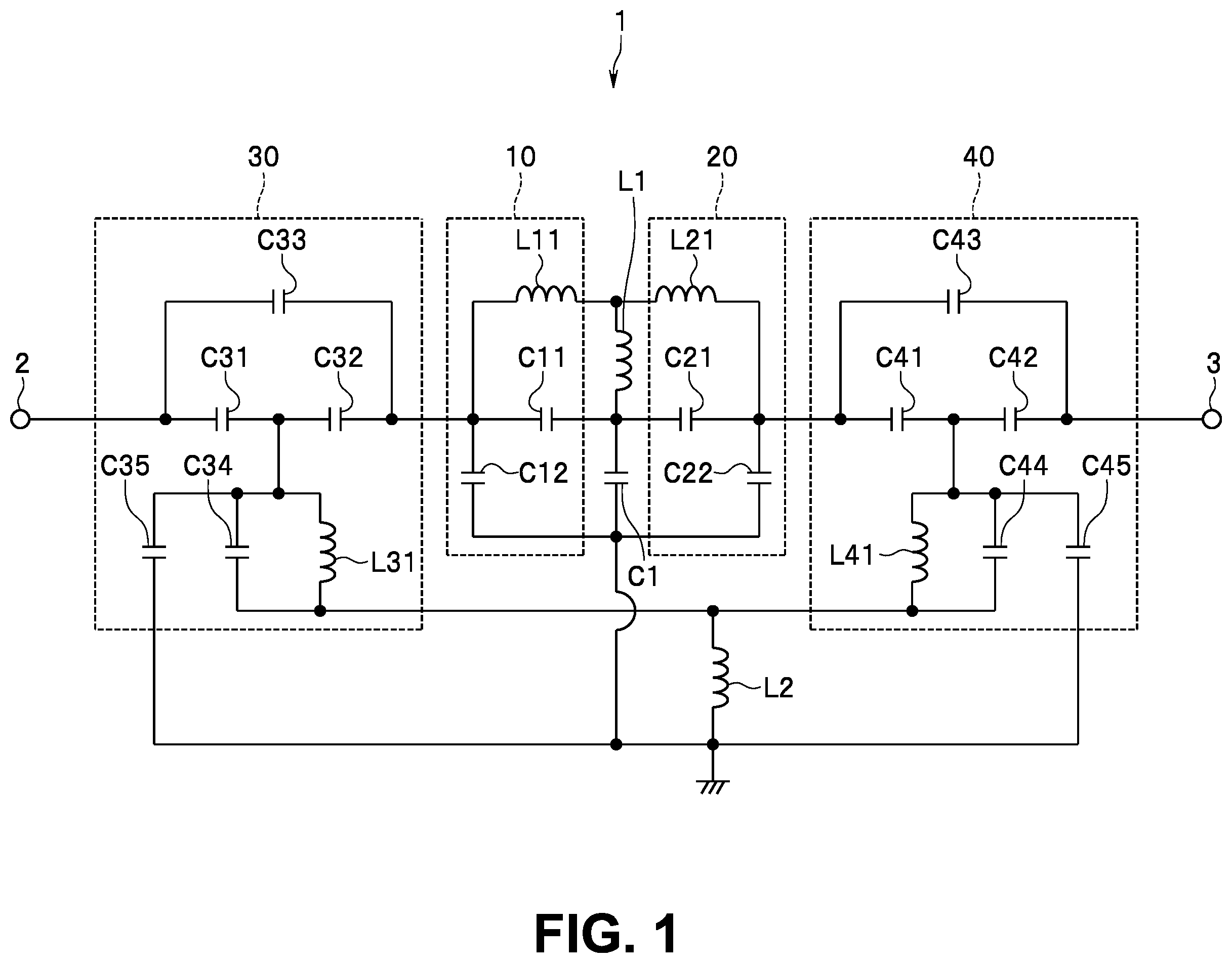
1 . A multilayered filter device comprising: a first filter which is a low-pass filter including a first inductor; a second filter which is a low-pass filter including a second inductor; a third filter which is a high-pass filter including a third inductor; a fourth filter which is a high-pass filter including a fourth inductor; and a stack for integrating the first filter, the second filter, the third filter, and the fourth filter, the stack including a plurality of dielectric layers stacked together, wherein each of the first inductor, the second inductor, the third inductor, and the fourth inductor is wound around an axis orthogonal to a stacking direction of the dielectric layers, the first inductor, the second inductor, the third inductor, and the fourth inductor are arranged in a manner that an opening of the first inductor and an opening of the third inductor face each other, an opening of the second inductor and an opening of the fourth inductor face each other, the opening of the first inductor and the opening of the second inductor do not face each other, and the opening of the third inductor and the opening of the fourth inductor do not face each other, and the first filter and the second filter are provided between the third filter and the fourth filter in a circuit configuration.
11 . A multilayered filter device comprising: a first filter which is a low-pass filter including a first inductor; a second filter which is a low-pass filter including a second inductor; a third filter which is a high-pass filter including a third inductor; a fourth filter which is a high-pass filter including a fourth inductor; and a stack for integrating the first filter, the second filter, the third filter, and the fourth filter, the stack including a plurality of dielectric layers stacked together, wherein each of the first inductor, the second inductor, the third inductor, and the fourth inductor is wound around an axis orthogonal to a stacking direction of the dielectric layers, the first inductor, the second inductor, the third inductor, and the fourth inductor are arranged in a manner that an opening of the first inductor and an opening of the third inductor face each other, an opening of the second inductor and an opening of the fourth inductor face each other, the opening of the first inductor and the opening of the second inductor do not face each other, and the opening of the third inductor and the opening of the fourth inductor do not face each other, the first inductor and the third inductor are arranged along a first direction orthogonal to the stacking direction, the second inductor and the fourth inductor are arranged along the first direction, the first inductor and the second inductor are arranged along a second direction orthogonal to the stacking direction and the first direction, and the third inductor and the fourth inductor are arranged along the second direction.
12 . A multilayered filter device comprising: a first filter which is a low-pass filter including a first inductor; a second filter which is a low-pass filter including a second inductor; a third filter which is a high-pass filter including a third inductor; a fourth filter which is a high-pass filter including a fourth inductor; and a stack for integrating the first filter, the second filter, the third filter, and the fourth filter, the stack including a plurality of dielectric layers stacked together, wherein each of the first inductor, the second inductor, the third inductor, and the fourth inductor is wound around an axis orthogonal to a stacking direction of the dielectric layers, the first inductor, the second inductor, the third inductor, and the fourth inductor are arranged in a manner that an opening of the first inductor and an opening of the third inductor face each other, an opening of the second inductor and an opening of the fourth inductor face each other, the opening of the first inductor and the opening of the second inductor do not face each other, and the opening of the third inductor and the opening of the fourth inductor do not face each other, each of the first inductor, the second inductor, the third inductor, and the fourth inductor includes a first through hole line, a second through hole line, and an inductor conductor layer electrically connected to one end of the first through hole line and one end of the second through hole line, each of the first through hole line and the second through hole line is formed by a plurality of through holes being connected in series, the stack has a shape that is long in one direction orthogonal to the stacking direction in a plan view seen from the stacking direction, and the inductor conductor layer of each of the first inductor, the second inductor, the third inductor, and the fourth inductor extends along the one direction orthogonal to the stacking direction.
Show 9 dependent claims
2 . The multilayered filter device according to claim 1 , further comprising a first signal terminal and a second signal terminal each integrated with the stack, wherein the third filter is provided between the first signal terminal and the second signal terminal in the circuit configuration, and the fourth filter is provided between the third filter and the second signal terminal in the circuit configuration.
3 . The multilayered filter device according to claim 2 , wherein the first filter, the second filter, the third filter, and the fourth filter constitute a band-pass filter.
4 . The multilayered filter device according to claim 1 , further comprising an inductor connected to one end portion of each of the first inductor and the second inductor.
5 . The multilayered filter device according to claim 1 , further comprising an inductor connected to one end portion of each of the third inductor and the fourth inductor.
6 . The multilayered filter device according to claim 1 , wherein the first inductor and the second inductor are arranged in a direction orthogonal to the stacking direction.
7 . The multilayered filter device according to claim 1 , wherein the third inductor and the fourth inductor are arranged in a direction orthogonal to the stacking direction.
8 . The multilayered filter device according to claim 1 , further comprising a capacitor including a plurality of capacitor conductor layers provided in the stack, wherein each of the first inductor and the second inductor includes a first through hole line, a second through hole line, and an inductor conductor layer electrically connected to one end of the first through hole line and one end of the second through hole line, each of the first through hole line and the second through hole line is formed by a plurality of through holes being connected in series, and another end of the second through hole line of the first inductor and another end of the second through hole line of the second inductor are electrically connected to one capacitor conductor layer of the plurality of capacitor conductor layers.
9 . The multilayered filter device according to claim 8 , further comprising: a conductor layer electrically connected to the other end of the second through hole line of the first inductor and the other end of the second through hole line of the second inductor; and at least one through hole electrically connecting the conductor layer and the one capacitor conductor layer.
10 . The multilayered filter device according to claim 1 , wherein each of the third inductor and the fourth inductor includes a first through hole line, a second through hole line, and an inductor conductor layer electrically connected to one end of the first through hole line and one end of the second through hole line, each of the first through hole line and the second through hole line is formed by a plurality of through holes being connected in series, the multilayered filter device further comprises: a conductor layer electrically connected to another end of the second through hole line of the third inductor and another end of the second through hole line of the fourth inductor; and at least one through hole electrically connecting the conductor layer and ground.
Full Description
Show full text →
CROSS REFERENCE TO RELATED APPLICATIONS
This application claims the benefit of Japanese Priority Patent Application No. 2023-35506 filed on Mar. 8, 2023, the entire contents of which are incorporated herein by reference.
BACKGROUND OF THE INVENTION
1. Field of the Invention The present invention relates to a multilayered filter device including a low-pass filter and a high-pass filter. 2. Description of the Related Art One of electronic components used in a communication apparatus is a band-pass filter. Such a band-pass filter can be constituted, for example, by connecting a high-pass filter forming an attenuation pole on a low-frequency side of a passband of the band-pass filter and a low-pass filter forming an attenuation pole on a high-frequency side of the passband of the band-pass filter, in series. The recent market demands for reductions in size and footprint of compact mobile communication apparatuses and also requires miniaturization of band-pass filters for use in those communication apparatuses. One known example of a band-pass filter suitable for downsizing is a band-pass filter using a stack including a plurality of dielectric layers and a plurality of conductor layers stacked together. Each of a high-pass filter and a low-pass filter includes an inductor. One known example of such an inductor used for a band-pass filter using a stack is an inductor composed of a conductor layer and a plurality of through holes and wound around an axis orthogonal to a stacking direction of a plurality of dielectric layers. US 2013/0229241 A1 discloses a multilayer band pass filter that is not a band-pass filter composed of a high-pass filter and a low-pass filter but includes a plurality of inductors each wound around an axis orthogonal to a stacking direction of a plurality of dielectric layers. When a high-pass filter and a low-pass filter are integrated with a stack, reduction in size of the stack causes an unintended magnetic coupling occurring between the plurality of inductors in the stack to be too strong in some cases. This prevents desired characteristics from being achieved in some cases. In particular, in a band-pass filter composed of a plurality of high-pass filters and a plurality of low-pass filters, if magnetic coupling between a plurality of inductors of the plurality of high-pass filters is too strong, this may cause a problem that adjustment of an attenuation pole formed on a low-frequency side of a passband of the band-pass filter is difficult. Similarly, if magnetic coupling between a plurality of inductors of the plurality of low-pass filters is too strong, this may cause a problem that adjustment of an attenuation pole formed on a high-frequency side of the passband of the band-pass filter is difficult. The above-described problems apply, not only to a case of adjusting attenuation poles in a band-pass filter composed of a plurality of high-pass filters and a plurality of low-pass filters, but also to a case in general of performing adjustment of characteristics including adjustment of attenuation poles in a multilayered filter device including a plurality of high-pass filters and a plurality of low-pass filters.
SUMMARY OF THE INVENTION
An object of the present invention is to provide a multilayered filter device that is composed of a plurality of high-pass filters and a plurality of low-pass filters and can be miniaturized while facilitating adjustment of characteristics. A multilayered filter device of the present invention includes: a first filter which is a low-pass filter including a first inductor; a second filter which is a low-pass filter including a second inductor; a third filter which is a high-pass filter including a third inductor; a fourth filter which is a high-pass filter including a fourth inductor; and a stack for integrating the first filter, the second filter, the third filter, and the fourth filter, the stack including a plurality of dielectric layers stacked together. Each of the first inductor, the second inductor, the third inductor, and the fourth inductor is wound around an axis orthogonal to a stacking direction of the dielectric layers. The first inductor, the second inductor, the third inductor, and the fourth inductor are arranged in a manner that an opening of the first inductor and an opening of the third inductor face each other, an opening of the second inductor and an opening of the fourth inductor face each other, the opening of the first inductor and the opening of the second inductor do not face each other, and the opening of the third inductor and the opening of the fourth inductor do not face each other. In the multilayered filter device of the present invention, the first to the fourth inductors are arranged as described above. Thus, according to the present invention, it is possible to provide a multilayered filter device that can be miniaturized while facilitating adjustment of characteristics. Other and further objects, features, and advantages of the present invention will appear more fully from the following description.
BRIEF DESCRIPTION OF THE DRAWINGS
is a circuit diagram showing a circuit configuration of a multilayered filter device according to a first embodiment of the present invention. is a perspective view showing an external appearance of the multilayered filter device according to the first embodiment of the present invention. A to C are explanatory diagrams showing respective patterned surfaces of first to third dielectric layers of a stack of the multilayered filter device according to a first embodiment of the present invention. A to C are explanatory diagrams showing respective patterned surfaces of fourth to sixth dielectric layers of the stack of the multilayered filter device according to the first embodiment of the present invention. A is an explanatory diagram showing a patterned surface of a seventh dielectric layer of the stack of the multilayered filter device according to the first embodiment of the present invention. B is an explanatory diagram showing a patterned surface of each of eighth to seventeenth dielectric layers of the stack of the multilayered filter device according to the first embodiment of the present invention. C is an explanatory diagram showing a patterned surface of an eighteenth dielectric layer of the stack of the multilayered filter device according to the first embodiment of the present invention. A and B are explanatory diagrams showing respective patterned surfaces of nineteenth and twentieth dielectric layers of the stack of the multilayered filter device according to the first embodiment of the present invention. is a perspective view showing an internal structure of the stack of the multilayered filter device according to the first embodiment of the present invention. A is an explanatory diagram showing a patterned surface of a fifth dielectric layer of a stack of a multilayered filter device according to a second embodiment of the present invention. B is an explanatory diagram showing a patterned surface of each of sixth and seventh dielectric layers of the stack of the multilayered filter device according to the second embodiment of the present invention. is a perspective view showing an internal structure of the stack of the multilayered filter device according to the second embodiment of the present invention. is a characteristic chart showing an example of pass attenuation characteristics of a model of a first practical example. is a characteristic chart showing an example of pass attenuation characteristics of a model of a second practical example.
DETAILED
DESCRIPTION OF THE PREFERRED EMBODIMENTS
First Embodiment An embodiment of the present invention will be described below in detail with reference to the drawings. A configuration of a multilayered filter device (hereinafter, referred to simply as a filter device) 1 according to one embodiment of the present invention will initially be outlined with reference to . The filter device 1 includes a first signal terminal 2 , a second signal terminal 3 , a first filter 10 , a second filter 20 , a third filter 30 , and a fourth filter 40 . Each of the first and second signal terminals 2 and 3 is a terminal for inputting or outputting a signal. In other words, when a signal is input to the first signal terminal 2 , a signal is output from the second signal terminal 3 . When a signal is input to the second signal terminal 3 , a signal is output from the first signal terminal 2 . The first filter 10 is a low-pass filter including a first inductor. The second filter 20 is a low-pass filter including a second inductor. The third filter 30 is a high-pass filter including a third inductor. The fourth filter 40 is a high-pass filter including a fourth inductor. The first to fourth filters 10 , 20 , 30 , and 40 are provided between the first signal terminal 2 and the second signal terminal 3 in a circuit configuration. Note that, in the present application, the expression “in the(a) circuit configuration” is used to indicate not a layout in a physical configuration but a layout in a circuit diagram. Arrangement of the first to fourth filters 10 , 20 , 30 , and 40 will be described below in detail. The third filter 30 is provided between the first signal terminal 2 and the second signal terminal 3 in the circuit configuration. The fourth filter 40 is provided between the third filter 30 and the second signal terminal 3 in the circuit configuration. The first filter 10 and the second filter 20 are provided between the third filter 30 and the fourth filter 40 in the circuit configuration. In particular, in the present embodiment, the first to fourth filters 10 , 20 , 30 , and 40 are connected in series in the order of the third filter 30 (high-pass filter), the first filter 10 (low-pass filter), the second filter 20 (low-pass filter), and then the fourth filter 40 (high-pass filter) from the first signal terminal 2 toward the second signal terminal 3 . The first to fourth filters 10 , 20 , 30 , and 40 constitute a band-pass filter that selectively passes a signal of a frequency within a certain passband. Next, an example of a circuit configuration of the filter device 1 will be described with reference to . The third filter 30 is connected to the first signal terminal 2 . The third filter 30 includes a third inductor L 31 and capacitors C 31 , C 32 , C 33 , C 34 , and C 35 . One end of the capacitor C 31 is connected to the first signal terminal 2 . One end of the capacitor C 32 is connected to the other end of the capacitor C 31 . One end of the capacitor C 33 is connected to the one end of the capacitor C 31 . The other end of the capacitor C 33 is connected to the other end of the capacitor C 32 . One end of the third inductor L 31 is connected to a connection point between the capacitor C 31 and the capacitor C 32 . The capacitor C 34 is connected in parallel with the third inductor L 31 . One end of the capacitor C 35 is connected to the connection point between the capacitor C 31 and the capacitor C 32 . The other end of the capacitor C 35 is grounded. The first filter 10 is connected to the third filter 30 . The first filter 10 includes a first inductor L 11 and capacitors C 11 and C 12 . One end of each of the first inductor L 11 and the capacitor C 11 is connected to the other end of the capacitor C 32 of the third filter 30 . One end of the capacitor C 12 is connected to the one end of the capacitor C 11 . The second filter 20 is connected to the first filter 10 . The second filter 20 includes a second inductor L 21 and capacitors C 21 and C 22 . One end of the second inductor L 21 is connected to the other end of the first inductor L 11 of the first filter 10 . One end of the capacitor C 21 is connected to the other end of the capacitor C 11 of the first filter 10 . One end of the capacitor C 22 is connected to the other end of the capacitor C 21 . The filter device 1 further includes an inductor L 1 and the capacitor C 1 . One end of the inductor L 1 is connected to a connection point between the first inductor L 11 and the second inductor L 21 . The other end of the inductor L 1 is connected to a connection point between the capacitor C 11 and the capacitor C 21 . One end of the capacitor C 1 is connected to the other end of the inductor L 1 . The other end of the capacitor C 1 is grounded. The fourth filter 40 is connected to the second filter 20 and the second signal terminal 3 . The fourth filter 40 includes a fourth inductor L 41 and capacitors C 41 , C 42 , C 43 , C 44 , and C 45 . One end of the capacitor C 41 is connected to the other end of the second inductor L 21 of the second filter 20 . One end of the capacitor C 42 is connected to the other end of the capacitor C 41 . The other end of the capacitor C 42 is connected to the second signal terminal 3 . One end of the capacitor C 43 is connected to the one end of the capacitor C 41 . The other end of the capacitor C 43 is connected to the other end of the capacitor C 42 . One end of the fourth inductor L 41 is connected to a connection point between the capacitor C 41 and the capacitor C 42 . The capacitor C 44 is connected in parallel with the fourth inductor L 41 . One end of the capacitor C 45 is connected to the connection point between the capacitor C 41 and the capacitor C 42 . The other end of the capacitor C 45 is grounded. The filter device 1 further includes an inductor L 2 . One end of the inductor L 2 is connected to the other end of each of the third and fourth inductors L 31 and L 41 . The other end of the inductor L 2 is grounded. In the example shown in , the first filter 10 and the second filter 20 have circuit configurations symmetric with respect to the inductors L 1 and L 2 and the capacitor C 1 . Specifically, in the filter device 1 , arrangements of the inductor and the capacitors included in the first filter 10 and the inductor and the capacitors included in the second filter 20 are symmetric with respect to the inductors L 1 and L 2 and the capacitor C 1 in a circuit diagram. Similarly, in the example shown in , the third filter 30 and the fourth filter 40 have circuit configurations symmetric with respect to the inductors L 1 and L 2 and the capacitor C 1 . Specifically, in the filter device 1 , arrangements of the inductor and the capacitors included in the third filter 30 and the inductor and the capacitors included in the fourth filter 40 are symmetric with respect to the inductors L 1 and L 2 and the capacitor C 1 in the circuit diagram. Next, other configurations of the filter device 1 will be described with reference to . is a perspective view showing an external appearance of the filter device 1 . The filter device 1 further includes a stack 50 including a plurality of dielectric layers and a plurality of conductors (plurality of conductor layers and plurality of through holes) stacked together. The first signal terminal 2 , the second signal terminal 3 , the first to fourth filters 10 , 20 , 30 , and 40 , the inductors L 1 and L 2 , and the capacitor C 1 are integrated with the stack 50 . The stack 50 has a bottom surface 50 A and a top surface 50 B located at both ends in a stacking direction T of the plurality of dielectric layers, and four side surfaces 50 C to 50 F connecting the bottom surface 50 A and the top surface 50 B. The side surfaces 50 C and 50 D are opposite to each other. The side surfaces 50 E and 50 F are opposite to each other. The side surfaces 50 C to 50 F are perpendicular to the top surface 50 B and the bottom surface 50 A. Here, as shown in , an X direction, a Y direction, and a Z direction are defined. The X direction, the Y direction, and the Z direction are orthogonal to one another. In the present embodiment, a direction parallel to the stacking direction T is defined as the Z direction. A direction opposite to the X direction is defined as a −X direction, a direction opposite to the Y direction is defined as a −Y direction, and a direction opposite to the Z direction is defined as a −Z direction. The expression of “when seen from the stacking direction T” means that an object is seen from a position away in the Z direction or the −Z direction. As shown in , the bottom surface 50 A is located at the end of the stack 50 in the −Z direction. The top surface 50 B is located at the end of the stack 50 in the Z direction. The side surface 50 C is located at the end of the stack 50 in the −X direction. The side surface 50 D is located at the end of the stack 50 in the X direction. The side surface 50 E is located at the end of the stack 50 in the −Y direction. The side surface 50 F is located at the end of the stack 50 in the Y direction. The filter device 1 further includes electrodes 111 , 112 , 113 , 114 , 115 , and 116 disposed on the bottom surface 50 A of the stack 50 . The electrodes 111 , 112 , and 113 are arranged in this order in the X direction at a position closer to the side surface 50 E than the side surface 50 F. The electrodes 114 , 115 , and 115 are arranged in this order in the −X direction at a position closer to the side surface 50 F than the side surface 50 E. The electrode 116 corresponds to the first signal terminal 2 , and the electrode 114 corresponds to the second signal terminal 3 . The first and second signal terminals 2 and 3 are thus disposed on the bottom surface 50 A of the stack 50 . Each of the electrodes 111 to 113 and 115 is grounded. Next, an example of the plurality of dielectric layers and the plurality of conductors constituting the stack 50 will be described with reference to A to B . In the present example, the stack 50 includes twenty dielectric layers stacked together. The twenty dielectric layers are hereinafter referred to as first to twentieth dielectric layers in the order from bottom to top. The first to twentieth dielectric layers are denoted by reference numerals 51 to 70 , respectively. In A to C , each circle represents a through hole. The dielectric layers 51 to 68 each have a plurality of through holes. The plurality of through holes are each formed by filling a hole intended for a through hole with a conductive paste. Each of the plurality of through holes is connected to an electrode, a conductor layer, or another through hole. For a connection relationship between each of the plurality of through holes and an electrode, a conductor layer, or another through hole, the connection relationship in a state where the first to twentieth dielectric layers 51 to 70 are stacked together is described. A shows a patterned surface of the first dielectric layer 51 . The electrodes 111 to 116 are formed on the patterned surface of the dielectric layer 51 . Through holes 51 T 1 , 51 T 3 , 51 T 4 , and 51 T 6 connected respectively to the electrodes 111 , 113 , 114 , and 116 , two through holes 51 T 2 connected to the electrode 112 , and two through holes 51 T 5 connected to the electrode 115 are formed in the dielectric layer 51 . B shows a patterned surface of the second dielectric layer 52 . Conductor layers 521 , 522 , 523 , 524 , and 525 are formed on the patterned surface of the dielectric layer 52 . The conductor layers 523 and 524 are connected to the conductor layer 525 . In B , each of a boundary between the conductor layer 523 and the conductor layer 525 and a boundary between the conductor layer 524 and the conductor layer 525 is indicated by a dotted line. The through hole 51 T 4 is connected to the conductor layer 522 . The through hole 51 T 6 is connected to the conductor layer 521 . Through holes 52 T 1 , 52 T 2 , and 52 T 3 are formed in the dielectric layer 52 . The through holes 51 T 1 to 51 T 3 , 51 T 5 , and 52 T 1 to 52 T 3 are connected to the conductor layer 523 . C shows a patterned surface of the third dielectric layer 53 . Conductor layers 531 , 532 , 533 , 534 , 535 , 536 , 537 , and 538 are formed on the patterned surface of the dielectric layer 53 . The through holes 52 T 1 and 52 T 2 are connected respectively to the conductor layers 531 and 532 . Through holes 53 T 1 , 53 T 2 , 53 T 3 a , 53 T 3 b , 53 T 4 a , 53 T 4 b , and 53 T 5 are formed in the dielectric layer 53 . The through holes 53 T 1 , 53 T 2 , and 53 T 5 are connected respectively to the conductor layers 534 , 536 , and 537 . The through holes 53 T 3 a and 53 T 4 a are connected respectively to the conductor layers 533 and 535 . The through holes 52 T 3 , 53 T 3 b , and 53 T 4 b are connected to the conductor layer 538 . A shows a patterned surface of the fourth dielectric layer 54 . Conductor layers 541 , 542 , 543 , 544 , 545 , and 546 are formed on the patterned surface of the dielectric layer 54 . The conductor layer 543 is connected to the conductor layer 541 . The conductor layer 544 is connected to the conductor layer 542 . In A , each of a boundary between the conductor layer 541 and the conductor layer 543 and a boundary between the conductor layer 542 and the conductor layer 544 is indicated by a dotted line. Two through holes 54 T 1 a , two through holes 54 T 2 a , and through holes 54 T 3 a , 54 T 3 b , 54 T 4 a , 54 T 4 b , and 54 T 5 are formed in the dielectric layer 54 . The two through holes 54 T 1 a are connected to the conductor layer 541 . The two through holes 54 T 2 a are connected to the conductor layer 542 . The through holes 53 T 3 a , 53 T 4 a , and 53 T 5 are connected respectively to the through holes 54 T 3 a , 54 T 4 a , and 54 T 5 . The through holes 53 T 3 b and 54 T 3 b are connected to the conductor layer 545 . The through holes 53 T 4 b and 54 T 4 b are connected to the conductor layer 546 . B shows a patterned surface of the fifth dielectric layer 55 . Conductor layers 551 , 552 , and 553 are formed on the patterned surface of the dielectric layer 55 . The conductor layers 551 and 552 are connected to the conductor layer 553 . In B , each of a boundary between the conductor layer 551 and the conductor layer 553 and a boundary between the conductor layer 552 and the conductor layer 553 is indicated by a dotted line. The two through holes 55 T 1 a , two through holes 55 T 2 a , and through holes 55 T 3 a , 55 T 3 b , 55 T 4 a , 55 T 4 b , and 55 T 5 are formed in the dielectric layer 55 . The through holes 54 T 1 a , 54 T 2 a , 54 T 3 a , 54 T 3 b , 54 T 4 a , and 54 T 4 b are connected respectively to the through holes 55 T 1 a , 55 T 2 a , 55 T 3 a , 55 T 3 b , 55 T 4 a , and 55 T 4 b . The through holes 54 T 5 and 55 T 5 are connected to the conductor layer 553 . C shows a patterned surface of the sixth dielectric layer 56 . Two through holes 56 T 1 a , two through holes 56 T 2 a , and through holes 56 T 3 a , 56 T 3 b , 56 T 4 a , 56 T 4 b , and 56 T 5 are formed in the dielectric layer 56 . The through holes 55 T 1 a , 55 T 2 a , 55 T 3 a , 55 T 3 b , 55 T 4 a , 55 T 4 b , and 55 T 5 are connected respectively to the through holes 56 T 1 a , 56 T 2 a , 56 T 3 a , 56 T 3 b , 56 T 4 a , 56 T 4 b , and 56 T 5 . A shows a patterned surface of the seventh dielectric layer 57 . A conductor layer 574 is formed on the patterned surface of the dielectric layer 57 . Two through holes 57 T 1 a , two through holes 57 T 1 b , two through holes 57 T 2 a , two through holes 57 T 2 b , and through holes 57 T 3 a , 57 T 3 b , 57 T 4 a , and 57 T 4 b are formed in the dielectric layer 57 . The through holes 56 T 1 a , 56 T 2 a , 56 T 3 a , 56 T 3 b , 56 T 4 a , and 56 T 4 b are connected respectively to the through holes 57 T 1 a , 57 T 2 a , 57 T 3 a , 57 T 3 b , 57 T 4 a , and 57 T 4 b . The through hole 56 T 5 , the two through holes 57 T 1 b , and the two through holes 57 T 2 b are connected to the conductor layer 574 . B shows a patterned surface of each of the eighth to seventeenth dielectric layers 58 to 67 . Two through holes 58 T 1 a , two through holes 58 T 1 b , two through holes 58 T 2 a , two through holes 58 T 2 b , and through holes 58 T 3 a , 58 T 3 b , 58 T 4 a , and 58 T 4 b are formed in each of the dielectric layers 58 to 67 . The through holes 57 T 1 a , 57 T 1 b , 57 T 2 a , 57 T 2 b , 57 T 3 a , 57 T 3 b , 57 T 4 a , and 57 T 4 b are connected respectively to the through holes 58 T 1 a , 58 T 1 b , 58 T 2 a , 58 T 2 b , 58 T 3 a , 58 T 3 b , 58 T 4 a , and 58 T 4 b formed in the dielectric layer 58 . In the dielectric layers 58 to 67 , every vertically adjacent through holes denoted by the same reference signs are connected to each other. C shows a patterned surface of the eighteenth dielectric layer 68 . Inductor conductor layers 681 , 682 , 683 , and 684 are formed on the patterned surface of the dielectric layer 68 . The conductor layer 681 has a first end and a second end located at both ends of the conductor layer 681 in a longitudinal direction. The conductor layer 682 has a first end and a second end located at both ends of the conductor layer 682 in a longitudinal direction. The conductor layer 683 has a first end and a second end located at both ends of the conductor layer 683 in a longitudinal direction. The conductor layer 684 has a first end and a second end located at both ends of the conductor layer 684 in a longitudinal direction. Two through holes 68 T 1 a , two through holes 68 T 1 b , two through holes 68 T 2 a , two through holes 68 T 2 b , and through holes 68 T 3 a , 68 T 3 b , 68 T 4 a , and 68 T 4 b are formed in the dielectric layer 68 . The two through holes 58 T 1 a formed in the dielectric layer 67 and the two through holes 68 T 1 a are connected to a portion near the first end of the conductor layer 681 . The two through holes 58 T 1 b formed in the dielectric layer 67 and the two through holes 68 T 1 b are connected to a portion near the second end of the conductor layer 681 . The two through holes 58 T 2 a formed in the dielectric layer 67 and the two through holes 68 T 2 a are connected to a portion near the first end of the conductor layer 682 . The two through holes 58 T 2 b formed in the dielectric layer 67 and the two through holes 68 T 2 b are connected to a portion near the second end of the conductor layer 682 . The through hole 58 T 3 a formed in the dielectric layer 67 and the through hole 68 T 3 a are connected to a portion near the first end of the conductor layer 683 . The through hole 58 T 3 b formed in the dielectric layer 67 and the through hole 68 T 3 b are connected to a portion near the second end of the conductor layer 683 . The through hole 58 T 4 a formed in the dielectric layer 67 and the through hole 68 T 4 a are connected to a portion near the first end of the conductor layer 684 . The through hole 58 T 4 b formed in the dielectric layer 67 and the through hole 68 T 4 b are connected to a portion near the second end of the conductor layer 684 . A shows a patterned surface of the nineteenth dielectric layer 69 . Inductor conductor layers 691 , 692 , 693 , and 694 are formed on the patterned surface of the dielectric layer 69 . The conductor layer 691 has a first end and a second end located at both ends of the conductor layer 691 in a longitudinal direction. The conductor layer 692 has a first end and a second end located at both ends of the conductor layer 692 in a longitudinal direction. The conductor layer 693 has a first end and a second end located at both ends of the conductor layer 693 in a longitudinal direction. The conductor layer 694 has a first end and a second end located at both ends of the conductor layer 694 in a longitudinal direction. The two through holes 68 T 1 a are connected to a portion near the first end of the conductor layer 691 . The two through holes 68 T 1 b are connected to a portion near the second end of the conductor layer 691 . The two through holes 68 T 2 a are connected to a portion near the first end of the conductor layer 692 . The two through holes 68 T 2 b are connected to a portion near the second end of the conductor layer 692 . The through hole 68 T 3 a is connected to a portion near the first end of the conductor layer 693 . The through hole 68 T 3 b is connected to a portion near the second end of the conductor layer 693 . The through hole 68 T 4 a is connected to a portion near the first end of the conductor layer 694 . The through hole 69 T 4 b is connected to a portion near the second end of the conductor layer 694 . B shows a patterned surface of the twentieth dielectric layer 70 . A mark 701 is formed on the patterned surface of the dielectric layer 70 . The stack 50 shown in is formed by stacking the first to twentieth dielectric layers 51 to 70 such that the patterned surface of the first dielectric layer 51 serves as the bottom surface 50 A of the stack 50 and the surface of the twentieth dielectric layer 70 opposite to the patterned surface thereof serves as the top surface 50 B of the stack 50 . shows an internal structure of the stack 50 formed by stacking the first to twentieth dielectric layers 51 to 70 . As shown in , the plurality of conductor layers and the plurality of through holes shown in A to A are stacked inside the stack 50 . In , the mark 701 is omitted. A correspondence between circuit components of the filter device 1 shown in and internal components of the stack 50 shown in A to A will now be described. Components of the first filter 10 will initially be described. The first inductor L 11 is composed of the inductor conductor layers 681 and 691 and the through holes 54 T 1 a , 55 T 1 a , 56 T 1 a , 57 T 1 a , 57 T 1 b , 58 T 1 a , 58 T 1 b , 68 T 1 a , and 68 T 1 b. The capacitor C 11 is composed of the conductor layers 541 and 551 and the dielectric layer 54 between those conductor layers. The capacitor C 12 is composed of the conductor layers 531 and 541 and the dielectric layer 53 between those conductor layers. Next, components of the second filter 20 will be described. The second inductor L 21 is composed of the inductor conductor layers 682 and 692 and the through holes 54 T 2 a , 55 T 2 a , 56 T 2 a , 57 T 2 a , 57 T 2 b , 58 T 2 a , 58 T 2 b , 68 T 2 a , and 68 T 2 b. The capacitor C 21 is composed of the conductor layers 542 and 552 and the dielectric layer 54 between those conductor layers. The capacitor C 22 is composed of the conductor layers 532 and 542 and the dielectric layer 53 between those conductor layers. Next, components of the third filter 30 will be described. The third inductor L 31 is composed of the inductor conductor layers 683 and 693 and the through holes 53 T 3 a , 54 T 3 a , 54 T 3 b , 55 T 3 a , 55 T 3 b , 56 T 3 a , 56 T 3 b , 57 T 3 a , 57 T 3 b , 58 T 3 a , 58 T 3 b , 68 T 3 a , and 68 T 3 b. The capacitor C 31 is composed of the conductor layers 521 and 533 and the dielectric layer 52 between those conductor layers. The capacitor C 32 is composed of the conductor layers 533 and 543 and the dielectric layer 53 between those conductor layers. The capacitor C 33 is composed of the conductor layers 521 and 534 and the dielectric layer 52 between those conductor layers. The capacitor C 34 is composed of the conductor layers 533 and 545 and the dielectric layer 53 between those conductor layers. The capacitor C 35 is composed of the conductor layers 523 and 533 and the dielectric layer 52 between those conductor layers. Next, components of the fourth filter 40 will be described. The fourth inductor L 41 is composed of the inductor conductor layers 684 and 694 and the through holes 53 T 4 a , 54 T 4 a , 54 T 4 b , 55 T 4 a , 55 T 4 b , 56 T 4 a , 56 T 4 b , 57 T 4 a , 57 T 4 b , 58 T 4 a , 58 T 4 b , 68 T 4 a , and 68 T 4 b. The capacitor C 41 is composed of the conductor layers 535 and 544 and the dielectric layer 53 between those conductor layers. The capacitor C 42 is composed of the conductor layers 522 and 535 and the dielectric layer 52 between those conductor layers. The capacitor C 43 is composed of the conductor layers 522 and 536 and the dielectric layer 52 between those conductor layers. The capacitor C 44 is composed of the conductor layers 535 and 546 and the dielectric layer 53 between those conductor layers. The capacitor C 45 is composed of the conductor layers 524 and 535 and the dielectric layer 52 between those conductor layers. Next, the inductors L 1 and L 2 and the capacitor C 1 will be described. The inductor L 1 is formed by the through holes 55 T 5 and 56 T 5 . The inductor L 2 is formed by the through holes 52 T 3 . The capacitor C 1 is composed of the conductor layers 525 and 537 and the dielectric layer 52 between those conductor layers. Next, structural characteristics of the filter device 1 according to the present embodiment will be described with reference to to . Each of the first inductor L 11 of the first filter 10 , the second inductor L 21 of the second filter 20 , the third inductor L 31 of the third filter 30 , and the fourth inductor L 41 of the fourth filter 40 is also a rectangular or approximately rectangular winding. For the rectangular or approximately rectangular winding, the number of windings may be counted, when the winding is regarded as a rectangle, as ¼, per side of the rectangle. The number of windings of each of the first to fourth inductors L 11 , L 21 , L 31 , and L 41 is ¾ or more. In the present embodiment, each of the first to fourth inductors L 11 , L 21 , L 31 , and L 41 is wound ¾ times around an axis orthogonal to the stacking direction T. The above-described axis may be an axis extending in a direction parallel to the Y direction or may be an axis extending in a direction inclined with respect to a direction parallel to the Y direction. As employed herein, a structure formed by connecting two or more through holes in series will be referred to as a through hole line. The first inductor L 11 includes two through hole lines T 1 a , two through hole lines T 1 b , the conductor layer 681 connected to one end of each of the two through hole lines T 1 a and one end of each of the two through hole lines T 1 b . The two through hole lines T 1 a are formed by the through holes 54 T 1 a , 55 T 1 a , 56 T 1 a , 57 T 1 a , and 58 T 1 a being connected in series. The two through hole lines T 1 b are formed by the through holes 57 T 1 b and 58 T 1 b being connected in series. The first inductor L 11 further includes the conductor layer 691 and through holes 68 T 1 a and 68 T 1 b electrically connecting the conductor layer 681 and the conductor layer 691 . The second inductor L 21 includes two through hole lines T 2 a , two through hole lines T 2 b , and the conductor layer 682 connected to one end of each of the two through hole lines T 2 a and one end of each of the two through hole lines T 2 b . The two through hole lines T 2 a are formed by the through holes 54 T 2 a , 55 T 2 a , 56 T 2 a , 57 T 2 a , and 58 T 2 a being connected in series. The two through hole lines T 2 b are formed by the through holes 57 T 2 b and 58 T 2 b being connected in series. The second inductor L 21 further includes the conductor layer 692 and the through holes 68 T 2 a and 68 T 2 b electrically connecting the conductor layer 682 and the conductor layer 692 . The third inductor L 31 includes a through hole line T 3 a , a through hole line T 3 b , and the conductor layer 683 connected to one end of the through hole line T 3 a and one end of the through hole line T 3 b . The through hole line T 3 a is formed by the through holes 53 T 3 a , 54 T 3 a , 55 T 3 a , 56 T 3 a , 57 T 3 a , and 58 T 3 a being connected in series. The through hole line T 3 b is formed by the through holes 54 T 3 b , 55 T 3 b , 56 T 3 b , 57 T 3 b , and 58 T 3 b being connected in series. The third inductor L 31 further includes the conductor layer 693 and the through holes 68 T 3 a and 68 T 3 b electrically connecting the conductor layer 683 and the conductor layer 693 . The fourth inductor L 41 includes a through hole line T 4 a , a through hole line T 4 b , and the conductor layer 684 connected to one end of the through hole line T 4 a and one end of the through hole line T 4 b . The through hole line T 4 a is formed by the through holes 53 T 4 a , 54 T 4 a , 55 T 4 a , 56 T 4 a , 57 T 4 a , and 58 T 4 a being connected in series. The through hole line T 4 b is formed by the through holes 54 T 4 b , 55 T 4 b , 56 T 4 b , 57 T 4 b , and 58 T 4 b being connected in series. The fourth inductor L 41 further includes the conductor layer 694 and the through holes 68 T 4 a and 68 T 4 b electrically connecting the conductor layer 684 and the conductor layer 694 . The first inductor L 11 has an opening surrounded by the two through hole lines T 1 a , the conductor layer 681 , and the two through hole lines T 1 b . The second inductor L 21 has an opening surrounded by the two through hole lines T 2 a , the conductor layer 682 , and the two through hole lines T 2 b . The third inductor L 31 has an opening surrounded by the through hole line T 3 a , the conductor layer 683 , and the through hole line T 3 b . The fourth inductor L 41 has an opening surrounded by the through hole line T 4 a , the conductor layer 684 , and the through hole line T 4 b. As shown in , the first to fourth inductors L 11 , L 21 , L 31 , and L 41 are arranged to satisfy first to fourth requirements below. The first requirement is that the opening of the first inductor L 11 and the opening of the third inductor L 31 face each other. The second requirement is that the opening of the second inductor L 21 and the opening of the fourth inductor L 41 face each other. The third requirement is that the opening of the first inductor L 11 and the opening of the second inductor L 21 do not face each other. The fourth requirement is that the opening of the third inductor L 31 and the opening of the fourth inductor L 41 do not face each other. In the present embodiment, the first inductor L 11 and the third inductor L 31 are arranged in a direction parallel to the Y direction so that the opening of the first inductor L 11 and the opening of the third inductor L 31 face each other (first requirement). The second inductor L 21 and the fourth inductor L 41 are arranged in a direction parallel to the Y direction so that the opening of the second inductor L 21 and the opening of the fourth inductor L 41 face each other (second requirement). The first inductor L 11 and the second inductor L 21 are arranged in a direction parallel to the X direction so that the opening of the first inductor L 11 and the opening of the second inductor L 21 do not face each other (third requirement). The third inductor L 31 and the fourth inductor L 41 are arranged in a direction parallel to the X direction so that the opening of the third inductor L 31 and the opening of the fourth inductor L 41 do not face each other (fourth requirement). In particular, in the present embodiment, the first to fourth inductors L 11 , L 21 , L 31 , and L 41 are arranged counterclockwise in the order of the first inductor L 11 , the second inductor L 21 , the fourth inductor L 41 , and then the third inductor L 31 when seen from the stacking direction T. As shown in , one end portion of each of the first and second inductors L 11 and L 21 is connected to the inductor L 1 . Specifically, one end portion of each of the two through hole lines T 1 b of the first inductor L 11 and one end portion of each of the two through hole lines T 2 b of the second inductor L 21 are electrically connected to the through hole 56 T 5 forming the inductor L 1 through the conductor layer 574 . As shown in , the inductor L 1 is connected to the capacitor C 1 . One end portion of each of the two through hole lines T 1 b of the first inductor L 11 and one end portion of each of the two through hole lines T 2 b of the second inductor L 21 are electrically connected to the conductor layer 537 composing the capacitor C 1 , via the conductor layer 574 , the through holes 56 T 5 and 55 T 5 , the conductor layer 553 , and the through holes 54 T 5 and 53 T 5 . As shown in , one end portion of each of the third and fourth inductors L 31 and L 41 is connected to the inductor L 2 . Specifically, the one end portion of the through hole line T 3 b of the third inductor L 31 and the one end portion of the through hole line T 4 b of the fourth inductor L 41 are electrically connected to the through hole 52 T 3 forming the inductor L 2 through the through holes 53 T 3 b and 53 T 4 b and the conductor layer 538 . As shown in , the inductor L 2 is grounded. The one end portion of the through hole line T 3 b of the third inductor L 31 and the one end portion of the through hole line T 4 b of the fourth inductor L 41 are electrically grounded via the through holes 53 T 3 b and 53 T 4 b , the conductor layer 538 , the through hole 52 T 3 , the conductor layer 525 , the through holes 51 T 1 to 51 T 3 , and 51 T 5 and the electrodes 111 to 113 , and 115 . Next, operation and effects of the filter device 1 according to the present embodiment will be described. In the present embodiment, the first to fourth inductors L 11 , L 21 , L 31 , and L 41 are arranged to satisfy the above-described first to fourth requirements. According to the present embodiment, in particular, by the third requirement, it is possible to prevent magnetic coupling between the first filter 10 and the second filter 20 , each of which is a low-pass filter, from being too strong compared with a case where the opening of the first inductor L 11 and the opening of the second inductor L 21 face each other. Thus, according to the present embodiment, with at least one of the first inductor L 11 and the second inductor L 21 , effects of adjustment of an attenuation pole formed on the high-frequency side of the passband can be relatively increased. According to the present embodiment, in particular, by the fourth requirement, it is possible to prevent magnetic coupling between the third filter 30 and the fourth filter 40 , each of which is a high-pass filter, from being too strong compared with a case where the opening of the third inductor L 31 and the opening of the fourth inductor L 41 face each other. With this, according to the present embodiment, with at least one of the third inductor L 31 and the fourth inductor L 41 , effects of adjustment of an attenuation pole formed on the low-frequency side of the passband can be relatively increased. According to the present embodiment, in particular, by the first and second requirements, it is possible to reduce a space for arranging the first to fourth inductors L 11 , L 21 , L 31 , and L 41 while satisfying the third and fourth requirements. With this, according to the present embodiment, the stack 50 , in other words, the filter device 1 , can be miniaturized. In view of the above, according to the present invention, it is possible to provide the filter device 1 that can be miniaturized while facilitating adjustment of characteristics. In the present embodiment, the one end portion of each of the first inductor L 11 and the second inductor L 21 is connected to the inductor L 1 . According to the present embodiment, by the inductor L 1 , the strength of magnetic coupling between the first inductor L 11 and the second inductor L 21 can be adjusted. In the present embodiment, the first inductor L 11 and the second inductor L 21 are arranged in a direction parallel to the X direction. With this, according to the present embodiment, it is structurally easy to connect the one end portion of each of the first inductor L 11 and the second inductor L 21 to the inductor L 1 . Note that, in the present embodiment, the first to fourth filters 10 , 20 , 30 , and 40 are connected in series in the order of the third filter 30 , the first filter 10 , the second filter 20 , and then the fourth filter 40 from the first signal terminal 2 toward the second signal terminal 3 . If the first to fourth filters 10 , 20 , 30 , and 40 are connected in series in the order of the first filter 10 (low-pass filter), the third filter 30 (high-pass filter), the fourth filter 40 (high-pass filter), and then the second filter 20 (low-pass filter) from the first signal terminal 2 toward the second signal terminal 3 , a plurality of capacitors are provided in a path connecting the one end of the first inductor L 11 and the other end of the second inductor L 21 . This prevents the inductor L 1 electrically connected to the one end portion of each of the first inductor L 11 and the second inductor L 21 from being provided. The order of connection of the first to fourth filters 10 , 20 , 30 , and 40 in the present embodiment is also a requirement for providing the inductor L 1 . In the present embodiment, the one end portion of each of the third inductor L 31 and the fourth inductor L 41 is connected to the inductor L 2 . According to the present embodiment, by the inductor L 2 , the strength of magnetic coupling between the third inductor L 31 and the fourth inductor L 41 can be adjusted. In the present embodiment, the third inductor L 31 and the fourth inductor L 41 are arranged in a direction parallel to the X direction. With this, according to the present embodiment, it is structurally easy to connect the one end portion of each of the third inductor L 31 and the fourth inductor L 41 to the inductor L 2 . Second Embodiment Next, a second embodiment of the present invention will be described. In the present embodiment, the stack 50 of the filter device 1 includes fifth to seventh dielectric layers 155 to 157 instead of the fifth to seventh dielectric layers 55 to 57 in the first embodiment. The stack 50 in the present embodiment is formed by stacking the first to fourth dielectric layers 51 to 54 (refer to A to A ), the fifth to seventh dielectric layers 155 to 157 , and the eighth to twentieth dielectric layers 58 to 70 (refer to B to B ). A plurality of conductor layers and a plurality of through holes formed in each of the fifth to seventh dielectric layers 155 to 157 will be described below with reference to A and B . A shows a patterned surface of the fifth dielectric layer 155 . Conductor layers 1551 , 1552 , and 1553 are formed on the patterned surface of the dielectric layer 155 . The conductor layers 1551 and 1552 are connected to the conductor layer 1553 . In A , each of a boundary between the conductor layer 1551 and the conductor layer 1553 and a boundary between the conductor layer 1552 and the conductor layer 1553 is indicated by a dotted line. Two through holes 155 T 1 a , two through holes 155 T 1 b , two through holes 155 T 2 a , two through holes 155 T 2 b , and through holes 155 T 3 a , 155 T 3 b , 155 T 4 a , and 155 T 4 b are formed in the dielectric layer 155 . The through holes 54 T 1 a , 54 T 2 a , 54 T 3 a , 54 T 3 b , 54 T 4 a , and 54 T 4 b (refer to A ) are connected respectively to the through holes 155 T 1 a , 155 T 2 a , 155 T 3 a , 155 T 3 b , 155 T 4 a , and 154 T 4 b . The through hole 54 T 5 (refer to A ) and the through holes 155 T 1 b and 155 T 2 b are connected to the conductor layer 1553 . B shows a patterned surface of each of the sixth and seventh dielectric layers 156 and 157 . Two through holes 156 T 1 a , two through holes 156 T 1 b , two through holes 156 T 2 a , two through holes 156 T 2 b , and through holes 156 T 3 a , 156 T 3 b , 156 T 4 a , and 156 T 4 b are formed in each of the dielectric layers 156 and 157 . The through holes 155 T 1 a , 155 T 1 b , 155 T 2 a , 155 T 2 b , 155 T 3 a , 155 T 3 b , 155 T 4 a , and 155 T 4 b are connected respectively to the through holes 156 T 1 a , 156 T 1 b , 156 T 2 a , 156 T 2 b , 156 T 3 a , 156 T 3 b , 156 T 4 a , and 156 T 4 b formed in the dielectric layer 156 . In the dielectric layers 156 and 157 , every vertically adjacent through holes denoted by the same reference signs are connected to each other. The through holes 156 T 1 a , 156 T 1 b , 156 T 2 a , 156 T 2 b , 156 T 3 a , 156 T 3 b , 156 T 4 a , and 156 T 4 b formed in the dielectric layer 157 are connected respectively to the through holes 58 T 1 a , 58 T 1 b , 58 T 2 a , 58 T 2 b , 58 T 3 a , 58 T 3 b , 58 T 4 a , and 58 T 4 b formed in the dielectric layer 58 (refer to B ). In the present embodiment, the capacitor C 11 is composed by using the conductor layer 1551 , instead of the conductor layer 551 . The capacitor C 21 is composed by using the conductor layer 1552 , instead of the conductor layer 552 . is a perspective view showing an internal structure of the stack 50 in the present embodiment. In the present embodiment, the two through hole lines T 1 b of the first inductor L 11 are formed by the through holes 155 T 1 b , 156 T 1 b , and 58 T 1 b being connected in series. The two through hole lines T 2 b of the second inductor L 21 are formed by the through holes 155 T 2 b , 156 T 2 b , and 58 T 2 b being connected in series. In the present embodiment, the inductor L 1 shown in in the first embodiment is not provided. One end of the capacitor C 1 shown in in the first embodiment is connected to the connection point between the first inductor L 11 and the second inductor L 21 and the connection point between the capacitor C 11 and the capacitor C 21 . One end portion of each of the two through hole lines T 1 b of the first inductor L 11 and one end portion of each of the two through hole lines T 2 b of the second inductor L 21 are electrically connected to the conductor layer 537 composing the capacitor C 1 , via the conductor layer 1553 and the through holes 54 T 5 and 53 T 5 (refer to C , A , and A ). The configuration, operation, and effects of the present embodiment are otherwise the same as those of the first embodiment. [Simulation] Next, an example of characteristics of the filter device 1 will be described with reference to the result of a simulation. The simulation used a model of a first practical example and a model of a second practical example. The model of the first practical example is a model of the filter device 1 according to the first embodiment. The model of the second practical example is a model of the filter device 1 according to the second embodiment. In the simulation, pass attenuation characteristics were obtained for each of the model of the first practical example and the model of the second practical example. is a characteristic chart showing the pass attenuation characteristics of the model of the first practical example. is a characteristic chart showing the pass attenuation characteristics of the model of the second practical example. In and , the horizontal axis represents frequency, and the vertical axis represents attenuation. As shown in and , the filter device 1 has excellent characteristics as a band-pass filter. As shown in and , the absolute value of attenuation of an attenuation pole closest to a passband on the high-frequency side of the passband is larger in the model of the second practical example. In the model of the second practical example, the inductor L 1 is not provided. In other words, magnetic coupling between the first inductor L 11 and the second inductor L 21 in the model of the second practical example is suppressed compared with that in the model of the first practical model. As understood from the result, by the inductor L 1 , the magnetic coupling between the first inductor L 11 and the second inductor L 21 can be adjusted. Note that the magnetic coupling between the first inductor L 11 and the second inductor L 21 can also be adjusted by adjusting the number and shape of through holes forming the inductor L 1 , other than by presence/absence of the inductor L 1 . For example, by increasing in size of the inductor L 1 in a direction parallel to the stacking direction T (reducing in size of the through hole lines T 1 b and T 2 b in the direction parallel to the stacking direction T), the magnetic coupling between the first inductor L 11 and the second inductor L 21 can be strengthened. The above description of the inductor L 1 also applies to the inductor L 2 . In other words, the magnetic coupling between the third inductor L 31 and the fourth inductor L 41 can be adjusted by the presence/absence of the inductor L 2 or by adjusting the number and shape of through holes forming the inductor L 2 . The present invention is not limited to the foregoing embodiments, and various modifications may be made thereto. For example, the configuration of each of the first to fourth filters 10 , 20 , 30 , and 40 in the present invention can be any without being limited to the examples shown in each of the embodiments as long as satisfying the requirements of the claims. The first to fourth filters 10 , 20 , 30 , and 40 of the present invention may be part of a branching filter. In the present invention, the first inductor L 11 and the third inductor L 31 may be arranged in a direction parallel to the X direction. In this case, the second inductor L 21 and the fourth inductor L 41 are arranged in a direction parallel to the X direction so as to satisfy the requirement that the opening of the first inductor L 11 and the opening of the second inductor L 21 do not face each other (third requirement) and the requirement that the opening of the third inductor L 31 and the opening of the fourth inductor L 41 do not face each other (fourth requirement). In other words, the first inductor L 11 and the fourth inductor L 41 are arranged in a direction parallel to the Y direction, and the second inductor L 21 and the third inductor L 31 are arranged in a direction parallel to the Y direction. In this case, the third inductor L 31 substantially corresponds to a “fourth inductor” of the present invention, and the fourth inductor L 41 substantially corresponds to a “third inductor” of the present invention. As described above, a multilayered filter device of the present invention includes: a first filter which is a low-pass filter including a first inductor; a second filter which is a low-pass filter including a second inductor; a third filter which is a high-pass filter including a third inductor; a fourth filter which is a high-pass filter including a fourth inductor; and a stack for integrating the first filter, the second filter, the third filter, and the fourth filter, the stack including a plurality of dielectric layers stacked together. Each of the first inductor, the second inductor, the third inductor, and the fourth inductor is wound around an axis orthogonal to a stacking direction of the dielectric layers. The first inductor, the second inductor, the third inductor, and the fourth inductor are arranged in a manner that an opening of the first inductor and an opening of the third inductor face each other, an opening of the second inductor and an opening of the fourth inductor face each other, the opening of the first inductor and the opening of the second inductor do not face each other, and the opening of the third inductor and the opening of the fourth inductor do not face each other. The multilayered filter device of the present invention may further include a first signal terminal and a second signal terminal each integrated with the stack. The third filter may be provided between the first signal terminal and the second signal terminal in a circuit configuration. The fourth filter may be provided between the third filter and the second signal terminal in the circuit configuration. The first filter and the second filter may be provided between the third filter and the fourth filter in the circuit configuration. The first filter, the second filter, the third filter, and the fourth filter may constitute a band-pass filter. The multilayered filter device of the present invention may further include an inductor connected to one end portion of each of the first inductor and the second inductor. The multilayered filter device of the present invention may further include an inductor connected to one end portion of each of the third inductor and the fourth inductor. In the multilayered filter device of the present invention, the first inductor and the second inductor may be arranged in a direction orthogonal to the stacking direction. In the multilayered filter device of the present invention, the third inductor and the fourth inductor may be arranged in a direction orthogonal to the stacking direction. The multilayered filter device of the present invention may further include a capacitor including a plurality of capacitor conductor layers provided in the stack. Each of the first inductor and the second inductor may include a first through hole line, a second through hole line, and an inductor conductor layer electrically connected to one end of the first through hole line and one end of the second through hole line. Each of the first through hole line and the second through hole line may be formed by a plurality of through holes being connected in series. The other end of the second through hole line of the first inductor and the other end of the second through hole line of the second inductor may be electrically connected to one capacitor conductor layer of the plurality of capacitor conductor layers. The multilayered filter device of the present invention may further include: a conductor layer electrically connected to the other end of the second through hole line of the first inductor and the other end of the second through hole line of the second inductor; and at least one through hole electrically connecting the conductor layer and the one capacitor conductor layer. In the multilayered filter device of the present invention, each of the third inductor and the fourth inductor may include a first through hole line, a second through hole line, and an inductor conductor layer electrically connected to one end of the first through hole line and one end of the second through hole line. Each of the first through hole line and the second through hole line may be formed by a plurality of through holes being connected in series. The multilayered filter device of the present invention may further include: a conductor layer electrically connected to the other end of the second through hole line of the third inductor and the other end of the second through hole line of the fourth inductor; and at least one through hole electrically connecting the conductor layer and the ground. Obviously, many modifications and variations of the present invention are possible in the light of the above teachings. Thus, it is to be understood that, within the scope of the appended claims and equivalents thereof, the invention may be practiced in other embodiments than the foregoing most preferable embodiment.
Figures (10)
Citations
This patent cites (3)
- US11757424
- US12334894
- US2013/0229241