Multilayer Ceramic Capacitor Including Internal Electrode Layers with Varying Coverages
Abstract
A multilayer ceramic capacitor includes a multilayer body and three or more external electrodes. A first internal electrode layer includes a first counter electrode portion, a first extension portion, and a second extension portion. The first counter electrode portion includes a first central region, a first connection region connected to the first extension portion, and a second connection region connected to the second extension portion. Coverages of the first and second connection regions with respect to the dielectric layers are higher than a coverage of the first central region with respect to the dielectric layers, and coverages of the first and second extension portions with respect to the dielectric layers are higher than the coverage of the first central region with respect to the dielectric layers.
Claims (20)
1 . A multilayer ceramic capacitor comprising: a multilayer body including a plurality of laminated dielectric layers, a plurality of internal electrode layers each laminated on a respective one of the plurality of dielectric layers, a first main surface and a second main surface opposed to each other in a lamination direction, a first end surface and a second end surface opposed to each other in a length direction orthogonal or substantially orthogonal to the lamination direction, and a first side surface and a second side surface opposed to each other in a width direction orthogonal or substantially orthogonal to the lamination direction and the length direction; and three or more external electrodes; wherein the plurality of internal electrode layers include a plurality of first internal electrode layers and a plurality of second internal electrode layers; the plurality of first internal electrode layers each include a first counter electrode portion opposed to a respective one of the plurality of second internal electrode layers with a respective one of the plurality of dielectric layers interposed therebetween, a first extension portion extending from the first counter electrode portion and extending toward and being exposed at a first surface portion of the multilayer body, and a second extension portion extending from the first counter electrode portion and extending toward and being exposed at a second surface portion of the multilayer body; the plurality of second internal electrode layers each include a second counter electrode portion opposed to a respective one of the plurality of first internal electrode layers with a respective one of the plurality of dielectric layers interposed therebetween, and a third extension portion extending from the second counter electrode portion and extending toward and being exposed at a third surface portion of the multilayer body; the three or more external electrodes include a first external electrode connected to the first extension portion, a second external electrode connected to the second extension portion, and a third external electrode connected to the third extension portion; the first counter electrode portion includes a first central region including a central portion of the first counter electrode portion, and a first peripheral region around the first central region; the first peripheral region includes a first connection region connected to the first extension portion, a second connection region connected to the second extension portion, and a portion other than the first connection region and the second connection region; a coverage of each of the first connection region and the second connection region with respect to the dielectric layers is higher than a coverage of the first central region with respect to the dielectric layers and higher than a coverage of the portion other than the first connection region and the second connection region of the first peripheral region with respect to the dielectric layers; coverages of the first extension portion and the second extension portion with respect to the dielectric layers are higher than the coverage of the first central region with respect to the dielectric layers; and in at least one of the plurality of first internal electrode layers, an average thickness of the first counter electrode portion is equal or substantially equal to an average thickness of at least one of the first and second connection regions.
Show 19 dependent claims
2 . The multilayer ceramic capacitor according to claim 1 , wherein at least a portion of the first surface portion is a portion of the first side surface; and at least a portion of the second surface portion is a portion of the second side surface.
3 . The multilayer ceramic capacitor according to claim 2 , wherein a length of the first extension portion in the length direction is shorter than a length of the first counter electrode portion in the length direction; and a length of the second extension portion in the length direction is shorter than a length of the first counter electrode portion in the length direction.
4 . The multilayer ceramic capacitor according to claim 1 , wherein the coverages of the first connection region and the second connection region with respect to the dielectric layers are about 72% or more; and the coverages of the first extension portion and the second extension portion with respect to the dielectric layers are about 72% or more.
5 . The multilayer ceramic capacitor according to claim 1 , wherein the second internal electrode layers each include a fourth extension portion extending from the second counter electrode portion and extending toward and being exposed at a fourth surface portion of the multilayer body; and the three or more external electrodes further include a fourth external electrode connected to the fourth extension portion.
6 . The multilayer ceramic capacitor according to claim 5 , wherein at least a portion of the third surface portion is a portion of the first end surface; and at least a portion of the fourth surface portion is a portion of the second end surface.
7 . The multilayer ceramic capacitor according to claim 6 , wherein a length of the third extension portion in the width direction is shorter than a length of the second counter electrode portion in the width direction; and a length of the fourth extension portion in the width direction is shorter than a length of the second counter electrode portion in the width direction.
8 . The multilayer ceramic capacitor according to claim 5 , wherein the second counter electrode portion includes a second central region including a central portion of the second counter electrode portion, and a second peripheral region around the second central region; the second peripheral region includes a third connection region connected to the third extension portion, a fourth connection region connected to the fourth extension portion, and a portion other than the third connection region and the fourth connection region; a coverage of each of the third connection region and the fourth connection region with respect to the dielectric layers is higher than a coverage of the second central region with respect to the dielectric layers and higher than a coverage of the portion other than the third connection region and the fourth connection region of the second peripheral region with respect to the dielectric layers; and coverages of the third extension portion and the fourth extension portion with respect to the dielectric layers are higher than the coverage of the second central region with respect to the dielectric layers.
9 . The multilayer ceramic capacitor according to claim 8 , wherein the coverages of the third connection region and the fourth connection region with respect to the dielectric layers are about 72% or more; and the coverages of the third extension portion and the fourth extension portion with respect to the dielectric layers are about 72% or more.
10 . The multilayer ceramic capacitor according to claim 1 , wherein the dielectric layers each include a thickness of about 0.3 μm or more and about 1.5 μm or less.
11 . The multilayer ceramic capacitor according to claim 1 , wherein the internal electrode layers each include a thickness of about 0.25 μm or more and about 0.6 μm or less.
12 . The multilayer ceramic capacitor according to claim 11 , wherein the internal electrode layers each include a thickness of about 0.25 μm or more and about 0.4 μm or less.
13 . The multilayer ceramic capacitor according to claim 1 , wherein an extending direction of the first extension portion is defined as a first extending direction; a length of the first extension portion in a direction orthogonal or substantially orthogonal to the first extending direction is shorter than a length of the first counter electrode portion in a direction orthogonal or substantially orthogonal to the first extending direction; an extending direction of the second extension portion is defined as a second extending direction; and a length of the second extension portion in a direction orthogonal or substantially orthogonal to the second extending direction is shorter than a length of the first counter electrode portion in a direction orthogonal or substantially orthogonal to the second extending direction.
14 . The multilayer ceramic capacitor according to claim 13 , wherein at least a portion of the first surface portion is a portion of the first side surface; and at least a portion of the second surface portion is a portion of the second side surface.
15 . The multilayer ceramic capacitor according to claim 13 , wherein at least a portion of the first surface portion is a portion of the first end surface; and at least a portion of the second surface portion is a portion of the second end surface.
16 . The multilayer ceramic capacitor according to claim 13 , wherein at least a portion of the first surface portion is a portion of the first side surface adjacent to the first end surface; and at least a portion of the second surface portion is a portion of the first side surface adjacent to the second end surface.
17 . The multilayer ceramic capacitor according to claim 1 , wherein each of the plurality of dielectric layers includes BaTiO 3 , CaTiO 3 , SrTiO 3 , or CaZrO 3 as a main component.
18 . The multilayer ceramic capacitor according to claim 17 , wherein each of the plurality of dielectric layers further includes a Mn compound, a Fe compound, a Cr compound, a Co compound, or Ni compound as a sub-component.
19 . The multilayer ceramic capacitor according to claim 1 , wherein a thickness of each of the plurality of dielectric layers is about 0.3 μm or more and about 1.5 μm or less.
20 . The multilayer ceramic capacitor according to claim 1 , wherein a number of the plurality of dielectric layers is 14 or more and 1000 or less.
Full Description
Show full text →
CROSS REFERENCE TO RELATED APPLICATIONS
This application is based on and claims the benefit of priority from Japanese Patent Application No. 2021-201981, filed on Dec. 13, 2021, the entire contents of which are hereby incorporated herein by reference.
BACKGROUND OF THE INVENTION
1. Field of the Invention The present invention relates to a multilayer ceramic capacitor. 2. Description of the Related Art Conventionally, multilayer ceramic capacitors have been known. For example, as a decoupling capacitor used for stabilizing a power supply voltage supplied to an integrated circuit component which operates at high speed, a multilayer feedthrough ceramic capacitor having a structure such as that disclosed in Japanese Patent Application Publication No. 2000-58376 has been known. The multilayer feedthrough ceramic capacitor described in Japanese Patent Application Publication No. 2000-58376 includes a ceramic base body. Inside the ceramic base body, a plurality of first internal electrodes and a plurality of second internal electrodes are alternately provided in the lamination direction. Both ends of the first internal electrodes extend toward and reach both end faces in the length direction of the ceramic base body, and both ends of the second internal electrodes extend toward and reach both end faces in the width direction of the ceramic base body. With an increase in performance of electronic devices on which such multilayer feedthrough ceramic capacitors are mounted, large capacitances of such multilayer feedthrough ceramic capacitors are required. Here, as one way to achieve larger capacitances, it is conceivable to increase the number of laminated layers in the effective portion by reducing the thicknesses of the internal electrodes. However, in a case in which the thicknesses of the internal electrodes are reduced, when the melting point of the metal powder used in the internal electrodes is lower than that of the dielectric powder, the internal electrodes are liquefied and coagulation occurs when the dielectric layers are sintered. In this case, the internal electrodes are divided into a plurality of pieces, and the coverage of the internal electrode layers with respect to the dielectric layers decreases. As a result, the area of the current path decreases due to the decrease in the metal ratio of the internal electrodes, and the resistance increases, such that the DC resistance (Rdc) increases. As a result, the characteristics of the multilayer ceramic capacitor may deteriorate. When a decrease in the coverage occurs at the extension portions of the internal electrodes that extend toward and reach the end surfaces or the side surfaces of the ceramic base body, the internal electrodes are not sufficiently exposed at the end surfaces or the side surfaces of the multilayer body, and the connectivity between the internal electrodes and the external electrodes decreases. When the connectivity between the internal electrode layers and the external electrodes decreases, the DC resistance (Rdc) may increase more significantly.
SUMMARY OF THE INVENTION
Preferred embodiments of the present invention provide multilayer ceramic capacitors that are each able to reduce or prevent an increase in DC resistance of internal electrode layers. A multilayer ceramic capacitor according to a preferred embodiment of the present invention includes a multilayer body including a plurality of laminated dielectric layers, a plurality of internal electrode layers each laminated on a respective one of the plurality of dielectric layers, a first main surface and a second main surface opposed to each other in a lamination direction, a first end surface and a second end surface opposed to each other in a length direction orthogonal or substantially orthogonal to the lamination direction, and a first side surface and a second side surface opposed to each other in a width direction orthogonal or substantially orthogonal to the lamination direction and the length direction, and three or more external electrodes, wherein the plurality of internal electrode layers include a plurality of first internal electrode layers and a plurality of second internal electrode layers, the plurality of first internal electrode layers each include a first counter electrode portion opposed to a respective one of the plurality of second internal electrode layers with a respective one of the plurality of dielectric layers interposed therebetween, a first extension portion that extends from the first counter electrode portion and extends towards and is exposed at a first surface portion of the multilayer body, and a second extension portion that extends from the first counter electrode portion and extends towards and is exposed at a second surface portion of the multilayer body, the plurality of second internal electrode layers each include a second counter electrode portion opposed to a respective one of the plurality of first internal electrode layers with a respective one of the plurality of dielectric layers interposed therebetween, and a third extension portion that extends from the second counter electrode portion and extends towards and is exposed at a third surface portion of the multilayer body, the three or more external electrodes include a first external electrode connected to the first extension portion, a second external electrode connected to the second extension portion, and a third external electrode connected to the third extension portion, the first counter electrode portion includes a first central region including a central portion of the first counter electrode portion, a first connection region that is connected to the first extension portion and has a higher coverage with respect to the dielectric layers than the first central region, and a second connection region that is connected to the second extension portion and has a higher coverage with respect to the dielectric layers than the first central region, the coverages of the first connection region and the second connection region with respect to the dielectric layers are higher than a coverage of the first central region with respect to the dielectric layers, and coverages of the first extension portion and the second extension portion with respect to the dielectric layers are higher than the coverage of the first central region with respect to the dielectric layers. According to preferred embodiments of the present invention, it is possible to provide multilayer ceramic capacitors that are each able to reduce or prevent an increase in DC resistance of internal electrode layers. The above and other elements, features, steps, characteristics and advantages of the present invention will become more apparent from the following detailed description of the preferred embodiments with reference to the attached drawings.
BRIEF DESCRIPTION OF THE DRAWINGS
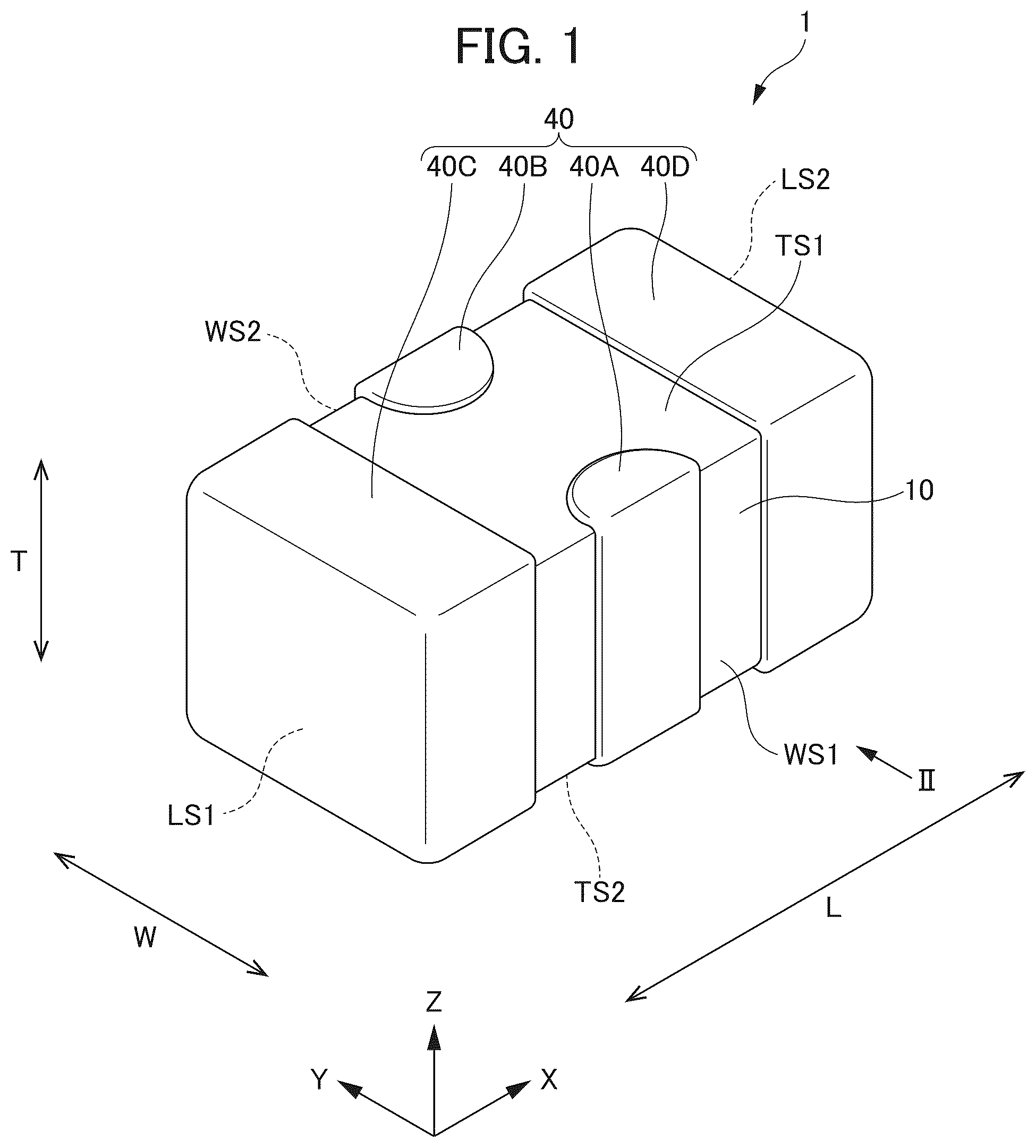
is an external perspective view of a multilayer ceramic capacitor according to a first preferred embodiment of the present invention. is an arrow view of the multilayer ceramic capacitor shown in when a first side surface is viewed along the direction of the arrow II. is an arrow view of the multilayer ceramic capacitor shown in when a first main surface is viewed along the direction of the arrow III. is a cross-sectional view taken along the line IV-IV of the multilayer ceramic capacitor shown in . is a cross-sectional view taken along the line V-V of the multilayer ceramic capacitor shown in . is a cross-sectional view taken along the line VI-VI of the multilayer ceramic capacitor shown in , showing first internal electrode layers. is a cross-sectional view taken along line VII-VII of the multilayer ceramic capacitor shown in , showing second internal electrode layers. A is a diagram showing measurement positions of the coverage of the first internal electrode layers with respect to dielectric layers. B is a diagram showing measurement positions of the coverage of the second internal electrode layers with respect to the dielectric layers. is a cross-sectional view showing a modified example of a second internal electrode layers of a multilayer ceramic capacitor according to a preferred embodiment of the present invention, and corresponds to . A is an external perspective view of a multilayer ceramic capacitor according to a second preferred embodiment of the present invention. B is a diagram showing a first internal electrode layer of the second preferred embodiment of the present invention. C shows a second internal electrode layer of the second preferred embodiment of the present invention. A is an external perspective view of a multilayer ceramic capacitor according to a third preferred embodiment of the present invention. B shows a first internal electrode layer of the third preferred embodiment of the present invention. C shows a second internal electrode layer of the third preferred embodiment of the present invention. A is a diagram showing a first internal electrode layer of a multilayer ceramic capacitor according to a fourth preferred embodiment of the present invention. B is a diagram showing a second internal electrode layer of the fourth preferred embodiment of the present invention. A is an external perspective view of a multilayer ceramic capacitor according to a fifth preferred embodiment of the present invention. B is a diagram showing a first internal electrode layer of the above preferred embodiment. C shows a second internal electrode layer of the fifth preferred embodiment of the present invention. A is an external perspective view of a multilayer ceramic capacitor according to a sixth preferred embodiment of the present invention. B is a diagram showing a first internal electrode layer of the sixth preferred embodiment of the present invention. C shows a second internal electrode layer of the sixth preferred embodiment of the present invention. A is an external perspective view of a multilayer ceramic capacitor according to a seventh preferred embodiment of the present invention. B is a diagram showing a first internal electrode layer of the seventh preferred embodiment of the present invention. C shows the second internal electrode layer of the seventh preferred embodiment of the present invention.
DETAILED
DESCRIPTION OF THE PREFERRED EMBODIMENTS
First Preferred Embodiment Hereinafter, a multilayer ceramic capacitor 1 according to a first preferred embodiment of the present invention will be described. is an external perspective view of a multilayer ceramic capacitor 1 according to the first preferred embodiment of the present invention. is an arrow view of the multilayer ceramic capacitor 1 shown in when the first side surface WS 1 is viewed along the direction of the arrow II. is an arrow view of the multilayer ceramic capacitor 1 shown in when the first main surface TS 1 is viewed along the direction of the arrow III. is a cross-sectional view taken along the line IV-IV of the multilayer ceramic capacitor 1 shown in . is a cross-sectional view taken along the line V-V of the multilayer ceramic capacitor 1 shown in . is a cross-sectional view taken along the line VI-VI of the multilayer ceramic capacitor 1 shown in , showing first internal electrode layers 31 . is a cross-sectional view taken along the line VII-VII of the multilayer ceramic capacitor 1 shown in , showing second internal electrode layers 32 . The multilayer ceramic capacitor 1 includes a multilayer body 10 and external electrodes 40 . to 7 show XYZ orthogonal coordinate systems. The length direction L of the multilayer ceramic capacitor 1 and the multilayer body 10 corresponds to the X direction. The width direction W of the multilayer ceramic capacitor 1 and the multilayer body 10 corresponds to the Y direction. The lamination (stacking) direction T of the multilayer ceramic capacitor 1 and the multilayer body 10 corresponds to the Z direction. Here, the cross section shown in is also referred to as a cross section LT. The cross section shown in is also referred to as a cross section WT. The cross section shown in is also referred to as a cross section LW. As shown in to 7 , the multilayer body 10 includes a first main surface TS 1 and a second main surface TS 2 which are opposed to each other in the lamination direction T, a first end surface LS 1 and a second end surface LS 2 which are opposed to each other in the length direction L orthogonal or substantially orthogonal to the lamination direction T, and a first side surface WS 1 and a second side surface WS 2 which are opposed to each other in the width direction W orthogonal or substantially orthogonal to the lamination direction T and the length direction L. As shown in , the multilayer body 10 has a rectangular or substantially rectangular parallelepiped shape. The dimension in the length direction L of the multilayer body 10 is not necessarily longer than the dimension in the width direction W. The corners and ridges of the multilayer body 10 are preferably rounded. The corner portions are portions where the three surfaces of the laminate intersect, and the ridge portions are portions where the two surfaces of the laminate intersect. In addition, unevenness or the like may be provided on a portion or the entirety of the surface of the multilayer body 10 . The dimensions of the multilayer body 10 are not particularly limited. As shown in , the multilayer body 10 includes an inner layer portion 11 , and a first main surface-side outer layer portion 12 and a second main surface-side outer layer portion 13 that sandwich the inner layer portion 11 in the lamination direction T. The inner layer portion 11 includes a plurality of dielectric layers 20 and a plurality of internal electrode layers 30 . The inner layer portion 11 includes, in the lamination direction T, internal electrode layers 30 from the internal electrode layer 30 located closest to the first main surface TS 1 to the internal electrode layer 30 located closest to the second main surface TS 2 . In the inner layer portion 11 , the plurality of internal electrode layers 30 are opposed to each other with the dielectric layer 20 interposed therebetween. The inner layer portion 11 generates a capacitance and defines and functions as a capacitor. The plurality of dielectric layers 20 are each made of a dielectric material. The dielectric material may be, for example, a dielectric ceramic including components such as BaTio 3 , CaTio 3 , SrTiO 3 , or CaZro 3 . Furthermore, the dielectric material may be obtained by adding a sub-component such as, for example, Mn compound, Fe compound, Cr compound, Co compound, and Ni compound to the main component. The thickness of the dielectric layer 20 is preferably, for example, about 0.3 μm or more and about 1.5 μm or less. The number of the dielectric layers 20 to be laminated (stacked) is preferably 14 or more and 1000 or less, for example. The number of the dielectric layers 20 refers to the total number of dielectric layers in the inner layer portion 11 , and dielectric layers in the first main surface-side outer layer portion 12 and the second main surface-side outer layer portion 13 . The plurality of internal electrode layers 30 include a plurality of first internal electrode layers 31 and a plurality of second internal electrode layers 32 . The plurality of first internal electrode layers 31 are provided on the plurality of dielectric layers 20 and extend toward the first side surface WS 1 and the second side surface WS 2 . The plurality of second internal electrode layers 32 are provided on the plurality of dielectric layers 20 and extend toward the first end surface LS 1 and the second end surface LS 2 . The plurality of first internal electrode layers 31 and the plurality of second internal electrode layers 32 are alternately provided with the dielectric layer 20 interposed therebetween in the lamination direction T of the multilayer body 10 . The first internal electrode layers 31 and the second internal electrode layers 32 each sandwich the dielectric layers 20 . As shown in , the first internal electrode layers 31 each include a first counter electrode portion 31 M opposed to the second internal electrode layer 32 with the dielectric layer 20 interposed therebetween, a first extension portion 31 A extending from the first counter electrode portion 31 M and extending towards and being exposed at a portion of the first side surface WS 1 defining and functioning as a first surface portion, and a second extension portion 31 B extending from the first counter electrode portion 31 M and extending towards and being exposed at a portion of the second side surface WS 2 defining and functioning as a second surface portion. The first extension portion 31 A is exposed at the first side surface WS 1 , and the second extension portion 31 B is exposed at the second side surface WS 2 . The shape of the first counter electrode portion 31 M is not particularly limited, but is preferably rectangular or substantially rectangular, for example. However, the corners of the rectangular or substantially rectangular shape may be rounded, or the corners of the rectangular or substantially rectangular shape may be oblique. The shapes of the first extension portion 31 A and the second extension portion 31 B are not particularly limited, but are preferably rectangular or substantially rectangular, for example. However, the corners of the rectangular or substantially rectangular shape may be rounded, or the corners of the rectangular or substantially rectangular shape may be oblique. The dimension L 2 of the first extension portion 31 A in the length direction L is smaller than the dimension L 1 of the first counter electrode portion 31 M in the length direction L. The dimension L 2 of the second extension portion 31 B in the length direction L is smaller than the dimension L 1 of the first counter electrode portion 31 M in the length direction L. That is, when the extending direction of the first extension portion 31 A (the direction from the second side surface WS 2 to the first side surface WS 1 ) is defined as the first extending direction, the length L 2 of the first extension portion 31 A in the direction orthogonal or substantially orthogonal to the first extending direction (the length direction L) is smaller than the length L 1 of the first counter electrode portion 31 M in the direction orthogonal or substantially orthogonal to the first extending direction (the length direction L). When the extending direction of the second extension portion 31 B (the direction from the first side surface WS 1 to the second side surface WS 2 ) is defined as the second extending direction, the length L 2 of the second extension portion 31 B in the direction orthogonal or substantially orthogonal direction to the second extending direction (the length direction L) is smaller than the length L 1 of the first counter electrode portion 31 M in the direction orthogonal or substantially orthogonal to the second extending direction (the length direction L). The length L 2 is preferably, for example, about 90% or less of the length L 1 . The length L 2 is more preferably, for example, about 5% or more and about 90% or less of the length L 1 . The first counter electrode portion 31 M includes a first central region 31 MM including a central portion of the first counter electrode portion 31 M, a first connection region 31 MA connected to the first extension portion 31 A, and a second connection region 31 MB connected to the second extension portion 31 B. The first connection region 31 MA has a higher coverage with respect to the dielectric layer 20 than the first central region 31 MM. The second connection region 31 MB has a higher coverage with respect to the dielectric layer 20 than the first central region 31 MM. The length of the first connection region 31 MA in the width direction W is defined as, for example, about 5% of the length W 1 of the first counter electrode portion 31 M in the width direction W. The length of the first connection region 31 MA in the length direction L is defined to be the same or substantially the same as the length L 2 of the first extension portion 31 A in the length direction L. The length of the second connection region 31 MB in the width direction W of the second connection region 31 MB is defined as, for example, about 5% of the length W 1 of the first counter electrode portion 31 M in the width direction W. The length of the second connection region 31 MB in the length direction L is defined to be the same or substantially the same as the length L 2 of the first extension portion 31 A in the length direction L. The coverage of the first connection region 31 MA and the second connection region 31 MB with respect to the dielectric layer 20 is higher than the coverage of the first central region 31 MM with respect to the dielectric layer 20 . The coverage of the first extension portion 31 A and the second extension portion 31 B with respect to the dielectric layer 20 is higher than the coverage of the first central region 31 MM with respect to the dielectric layer 20 . That is, when the coverage of the first central region 31 MM with respect to the dielectric layer 20 is defined as A, the coverage of the first connection region 31 MA and the second connection region 31 MB with respect to the dielectric layer 20 is defined as B, and the coverage of the first extension portion 31 A and the second extension portion 31 B with respect to the dielectric layer 20 is defined as C, the relationship of A<B and A<C are satisfied. With such a configuration, since the metal ratio of the first connection region 31 MA and the second connection region 31 MB of the first internal electrode layer 31 , and the metal ratio of the first extension portion 31 A and the second extension portion 31 B increase, it is possible to increase the area of the current path connecting the first internal electrode layer 31 and a first external electrode 40 A and a second external electrode 40 B, which will be described later, of the external electrode 40 . As a result, since the resistance of the first internal electrode layer 31 becomes low, it is possible to reduce or prevent an increase in the DC resistance (Rdc), and it is possible to maintain and improve the characteristics of the multilayer ceramic capacitor 1 . Furthermore, since it is possible to reduce or prevent the division of the first internal electrode layer 31 into a plurality of pieces, it is possible to reduce or prevent a decrease in the connectivity between the first internal electrode layer 31 , and the first external electrode 40 A and the second external electrode 40 B. With such a configuration, by providing the first connection region 31 MA and the second connection region 31 MB and making the coverage B of the first connection region 31 MA and the second connection region 31 MB with respect to the dielectric layer 20 larger than the coverage A of the first central region 31 MM with respect to the dielectric layer 20 , the metal ratio of the first internal electrode layer 31 increases not only in the first extension portion 31 A and the second extension portion 31 B, but also in the first connection region 31 MA and the second connection region 31 MB. With such a configuration, since it is possible to increase the area of the current path, it is possible to reduce the resistance correspondingly, and to reduce the resistance of the entire first internal electrode layer 31 . As a result, it is possible to further improve the advantageous effect of reducing or preventing an increase in DC resistance (Rdc). Here, in the present preferred embodiment, the reason why the coverage A of the first central region 31 MM is not equal to the coverage B of the first connection region 31 MA and the second connection region 31 MB or the coverage C of the first extension portion 31 A and the second extension portion 31 B will be described. In a case in which the coverage A of the first central region 31 MM is increased and is equal to or greater than the coverage B of the first connection region 31 MA and the second connection region 31 MB or the coverage C of the first extension portion 31 A and the second extension portion 31 B, although it is possible to ensure the capacitance, a portion where the dielectric layer 20 is exposed on the surface of the first internal electrode layer 31 may be reduced. In this case, the contact point between the dielectric layers 20 and the other dielectric layers 20 to be laminated on the first internal electrode layers 31 is reduced, and the adhesion strength is reduced, and there is a concern that delamination may occur. For example, when the coverage of the internal electrode layer with respect to the dielectric layer is 100%, delamination may be more likely to occur than when the coverage of the internal electrode layer with respect to the dielectric layer is low. In the present preferred embodiment, by making the coverage A of the first central region 31 MM lower than the coverage B of the first connection region 31 MA and the second connection region 31 MB and the coverage C of the first extension portion 31 A and the second extension portion 31 B, it is possible to ensure a portion where the dielectric layer 20 is exposed on the surface of the first internal electrode layer 31 , and it is possible to increase the contact point between the dielectric layers 20 and the other dielectric layers 20 to be laminated on the first internal electrode layers 31 . As a result, it is possible to ensure adhesion, and it is possible to reduce or prevent the delamination. According to the present preferred embodiment, it is possible to achieve both the reduction or prevention of an increase of the DC resistance (Rdc) of the first internal electrode layer 31 and a reduction or prevention of the delamination. That is, according to the multilayer ceramic capacitor 1 of the present preferred embodiment, an anchor effect is generated between the dielectric layers and the internal electrode layers, and thus, it is possible to increase the adhesion strength between the dielectric layers and the internal electrode layers. As a result, it is possible to reduce or prevent intrusion of moisture or the like into the multilayer body, and thus, it is possible to reduce or prevent a decrease in moisture resistance of the multilayer ceramic capacitor 1 . Therefore, it is possible to improve the reliability of the multilayer ceramic capacitor 1 while reducing or preventing an increase in the DC resistance (Rdc) of the first internal electrode layer 31 . Furthermore, the coverage B of the first connection region 31 MA and the second connection region 31 MB with respect to the dielectric layer 20 is preferably, for example, about 72% or more. The coverage C of the first extension portion 31 A and the second extension portion 31 B with respect to the dielectric layer 20 is preferably, for example, about 72% or more. The coverage A of the first central region 31 MM with respect to the dielectric layer 20 is preferably lower than the coverage B and the coverage C, and is preferably, for example, about 52% or more. The coverage B and the coverage C may be high at, for example, about 5% or more than the coverage A. As shown in , the second internal electrode layer 32 includes a second counter electrode portion 32 M opposed to the first internal electrode layer 31 with the dielectric layer 20 interposed therebetween, a third extension portion 32 C extending from the second counter electrode portion 32 M and extending toward and being exposed at a portion of the first end surface LS 1 defining and functioning as a third surface portion, and a fourth extension portion 32 D extending from the second counter electrode portion 32 M and extending towards and being exposed at a portion of the second end surface LS 2 defining and functioning as a fourth surface portion. The third extension portion 32 C is exposed at the first end surface LS 1 , and the fourth extension portion 32 D is exposed at the second end surface LS 2 . The shape of the second counter electrode portion 32 M is not particularly limited, but is preferably rectangular or substantially rectangular, for example. However, the corners of the rectangular or substantially rectangular shape may be rounded, or the corners of the rectangular or substantially rectangular shape may be provided obliquely. The shapes of the third extension portion 32 C and the fourth extension portion 32 D are not particularly limited, or but are preferably rectangular substantially rectangular, for example. However, the corners of the rectangular or substantially rectangular shape may be rounded, or the corners of the rectangular or substantially rectangular shape may be provided obliquely. The dimension W 2 of the third extension portion 32 C in the width direction W is equal to or smaller than the dimension W 1 of the second counter electrode portion 32 M in the width direction W. The dimension W 2 of the fourth extension portion 32 D in the width direction W is equal to or smaller than the dimension W 1 of the second counter electrode portion 32 M in the width direction W. In the present preferred embodiment, the dimension W 2 of the third extension portion 32 C in the width direction W is smaller than the dimension W 1 of the second counter electrode portion 32 M in the width direction W. The dimension W 2 of the fourth extension portion 32 D in the width direction W is smaller than the dimension W 1 of the second counter electrode portion 32 M in the width direction W. That is, when the extending direction of the third extension portion 32 C (the direction from the second end surface LS 2 toward the first end surface LS 1 ) is defined as the third extending direction, the length W 2 of the third extension portion 32 C in the direction orthogonal or substantially orthogonal to the third extending direction (the width direction W) is smaller than the length W 1 of the second counter electrode portion 32 M in the direction orthogonal or substantially orthogonal to the third extending direction (the width direction W). When the extending direction of the fourth extension portion 32 D (the direction from the first end surface LS 1 toward the second end surface LS 2 ) is defined as the fourth extending direction, the length W 2 of the fourth extension portion 32 D in the direction orthogonal or substantially orthogonal to the fourth extending direction (the width direction W) is smaller than the length W 1 of the second counter electrode portion 32 M in the orthogonal or substantially orthogonal to the fourth extending direction (the width direction W). The length W 2 is preferably, for example, about 90% or less of the length W 1 . The length W 2 is more preferably, for example, about 5% or more and about 90% or less of the length W 1 . The second counter electrode portion 32 M preferably includes a second central region 32 MM including a central portion of the second counter electrode portion 32 M, a third connection region 32 MC connected to the third extension portion 32 C, and a fourth connection region 32 MD connected to the fourth extension portion 32 D. The third connection region 32 MC has a higher coverage with respect to the dielectric layer 20 than the second central region 32 MM. The fourth connection region 32 MD has a higher coverage with respect to the dielectric layer 20 than the second central region 32 MM. The length of the third connection region 32 MC in the length direction L is defined as, for example, about 5% of the length L 1 of the second counter electrode portion 32 M in the length direction L. The length of the third connection region 32 MC in the width direction W is defined to be the same or substantially the same as the length W 2 of the third extension portion 32 C in the width direction W. The length of the fourth connection region 32 MD in the length direction L is defined as, for example, about 5% of the length L 1 of the second counter electrode portion 32 M in the length direction L. The length of the fourth connection region 32 MD in the width direction W is defined to be the same or substantially the same as the length W 2 of the fourth extension portion 32 D in the width direction W. The coverage of the third connection region 32 MC and the fourth connection region 32 MD with respect to the dielectric layer 20 is preferably higher than the coverage of the second central region 32 MM with respect to the dielectric layer 20 . The coverage of the third extension portion 32 C and the fourth extension portion 32 D with respect to the dielectric layer 20 is preferably higher than the coverage of the second central region 32 MM with respect to the dielectric layer 20 . That is, when the coverage of the second central region 32 MM with respect to the dielectric layer 20 is defined as D, the coverage of the third connection region 32 MC and the fourth connection region 32 MD with respect to the dielectric layer 20 is defined as E, and the coverage of the third extension portion 32 C and the fourth extension portion 32 D with respect to the dielectric layer 20 is defined as F, the relationship preferably satisfies D<E and D<F. With such a configuration, since the metal ratio of the third connection region 32 MC and the fourth connection region 32 MD of the second internal electrode layer 32 , and the metal ratio of the third extension portion 32 C and the fourth extension portion 32 D are increased, it is possible to increase the area of the current path connecting the second internal electrode layer 32 , and a third external electrode 40 C and a fourth external electrode 40 D, which will be described later, of the external electrodes 40 . As a result, since the resistance of the second internal electrode layer 32 becomes low, it is possible to reduce or prevent an increase in the DC resistance (Rdc), and it is possible to maintain and improve the characteristics of the multilayer ceramic capacitor 1 . Furthermore, since it is possible to reduce or prevent the division of the second internal electrode layer 32 into a plurality of pieces, it is possible to reduce or prevent a decrease in the connectivity between the second internal electrode layer 32 , and the third external electrode 40 C and the fourth external electrode 40 D. Thus, by providing the third connection region 32 MC and the fourth connection region 32 MD and making the coverage E of the third connection region 32 MC and the fourth connection region 32 MD with respect to the dielectric layer 20 larger than the coverage D of the second central region 32 MM with respect to the dielectric layer 20 , the metal ratio of the second internal electrode layer 32 is increased not only in the third extension portion 32 C and the fourth extension portion 32 D, but also in the third connection region 32 MC and the fourth connection region 32 MD. With such a configuration, since it is possible to increase the area of the current path, it possible to is reduce the resistance correspondingly, and thus it is possible to reduce the resistance of the entire second internal electrode layer 32 . As a result, it is possible to further improve the advantageous effect of reducing or preventing an increase in DC resistance (Rdc). Here, in the present preferred embodiment, the reason why the coverage D of the second central region 32 MM is not equal to the coverage E of the third connection region 32 MC and the fourth connection region 32 MD or the coverage F of the third extension portion 32 C and the fourth extension portion 32 D will be described. In a case in which the coverage D of the second central region 32 MM is increased and is equal to or greater than the coverage E of the third connection region 32 MC and the fourth connection region 32 MD or the coverage F of the third extension portion 32 C and the fourth extension portion 32 D, although it is possible to ensure the capacitance, a portion where the dielectric layer 20 is exposed on the surface of the second internal electrode layer 32 may be reduced. In this case, the contact point between the dielectric layers 20 and the other dielectric layers 20 to be laminated on the second internal electrode layers 32 is reduced, the adhesion strength is reduced, and there is a concern that delamination may occur. For example, when the coverage of the internal electrode layer with respect to the dielectric layer is 100%, delamination may be more likely to occur than when the coverage of the internal electrode layer with respect to the dielectric layer is low. In the present preferred embodiment, by making the coverage D of the second central region 32 MM lower than the coverage E of the third connection region 32 MC and the fourth connection region 32 MD and the coverage F of the third extension portion 32 C and the fourth extension portion 32 D, it is possible to ensure a portion where the dielectric layer 20 is exposed on the surface of the second internal electrode layer 32 , and it is possible to increase the contact point between the dielectric layers 20 and the other dielectric layers 20 to be laminated on the second internal electrode layers 32 . As a result, it is possible to ensure adhesion, and it is possible to reduce or prevent delamination. According to the present preferred embodiment, it is possible to achieve both a reduction or prevention of increase of the DC resistance (Rdc) of the second internal electrode layer 32 and the reduction or prevention of the delamination. That is, according to the multilayer ceramic capacitor 1 of the present preferred embodiment, an anchor effect is generated between the dielectric layers and the internal electrode layers, and thus, it is possible to increase the adhesion strength between the dielectric layers and the internal electrode layers. As a result, it is possible to reduce or prevent intrusion of moisture or the like into the multilayer body, and thus, it is possible to reduce or prevent a decrease in moisture resistance of the multilayer ceramic capacitor 1 . Therefore, it is possible to improve the reliability of the multilayer ceramic capacitor 1 while reducing or preventing an increase in the DC resistance (Rdc) of the second internal electrode layer 32 . The coverage E of the third connection region 32 MC and the fourth connection region 32 MD with respect to the dielectric layer 20 is preferably, for example, about 72% or more. The coverage F of the third extension portion 32 C and the second extension portion 32 D with respect to the dielectric layer 20 is preferably, for example, 72% or more. The coverage D of the second central region 32 MM with respect to the dielectric layer 20 is preferably lower than the coverage E and the coverage F, and is preferably, for example, about 52% or more. The coverage E and the coverage F may be high at, for example, about 5% or more than the coverage D. Furthermore, the first internal electrode layers 31 may be each used as a ground electrode in a multilayer feedthrough ceramic capacitor. The second internal electrode layers 32 may be each used as a through electrode in the multilayer feedthrough ceramic capacitor. The first internal electrode layers 31 and the second internal electrode layers 32 are each made of an appropriate electrically conductive material such as a metal such as, for example, Ni, Cu, Ag, Pd, or Au, or an alloy including at least one of these metals. When an alloy is used, the first internal electrode layers 31 and the second internal electrode layers 32 may be each made of, for example, an Ag—Pd alloy. The total number of the first internal electrode layers 31 and the second internal electrode layers 32 is preferably equal to or greater than 14 and equal to or less than 1000, for example. The number of the first internal electrode layers 31 is not particularly limited, but is preferably, for example, 7 or more and 500 or less. The number of the second internal electrode layers 32 is not particularly limited, but is preferably, for example, 7 or more and 500 or less. The thicknesses of the first counter electrode portion 31 M of the first internal electrode layer 31 and the second counter electrode portion 32 M of the second internal electrode layer 32 are not particularly limited, but are preferably, for example, about 0.25 μm or more and about 0.60 μm or less. In the present preferred embodiment, particularly high advantageous effects are achieved in regions each having a thickness of, for example, about 0.4 μm or less. The thicknesses of the first extension portion 31 A and the second extension portion 31 B of the first internal electrode layer 31 and the thicknesses of the third extension portion 32 C and the fourth extension portion 32 D of the second internal electrode layer 32 are not particularly limited, but are preferably, for example, about 0.25 μm or more and about 0.60 μm or less. In the present preferred embodiment, particularly high advantageous effects are achieved in regions each having a thickness of, for example, about 0.4 μm or less. The first main surface-side outer layer portion 12 is positioned adjacent to the first main surface TS 1 of the multilayer body 10 . The first main surface-side outer layer portion 12 is an aggregate of a plurality of dielectric layers 20 positioned between the first main surface TS 1 and the internal electrode layer 30 closest to the first main surface TS 1 . The dielectric layer 20 used in the first main surface-side outer layer portion 12 may be the same or substantially the same as the dielectric layer 20 used in the inner layer portion 11 . The second main surface-side outer layer portion 13 is positioned adjacent to the second main surface TS 2 of the multilayer body 10 . The second main surface-side outer layer portion 13 is an aggregate of a plurality of dielectric layers 20 positioned between the second main surface TS 2 and the internal electrode layer 30 closest to the second main surface TS 2 . The dielectric layer 20 used in the second main surface-side outer layer portion 13 may be the same or substantially the same as the dielectric layer 20 used in the inner layer portion 11 . As described above, the multilayer body 10 includes the plurality of laminated dielectric layers 20 and the plurality of internal electrode layers 30 laminated on the dielectric layers 20 . That is, the multilayer ceramic capacitor 1 includes the multilayer body 10 in which the dielectric layers 20 and the internal electrode layers 30 are alternately laminated. The multilayer body 10 includes a counter portion 11 E. The counter portion 11 E is a portion where the first counter electrode portion 31 M of the first internal electrode layer 31 and the second counter electrode portion 32 M of the second internal electrode layer 32 are opposed to each other. The counter portion 11 E is provided as a portion of the inner layer portion 11 . each show ranges of the counter portion 11 E in the width direction W and the length direction L. The counter portion 11 E is also referred to as a capacitor effective portion. The multilayer body 10 includes a side surface-side outer layer portion. The side surface-side outer layer portion includes a first side surface-side outer layer portion WG 1 positioned adjacent to the first side surface WS 1 and a second side surface-side outer layer portion WG 2 positioned adjacent to the second side surface WS 2 . The first side surface-side outer layer portion WG 1 is a portion including the dielectric layer 20 and the first extension portion 31 A positioned between the counter portion 11 E and the first side surface WS 1 . That is, the first side surface-side outer layer portion WG 1 is an aggregate of the portions of the plurality of dielectric layers 20 adjacent to the first side surface WS 1 and the plurality of first extension portions 31 A. The second side surface-side outer layer portion WG 2 is a portion including the dielectric layer 20 and the second extension portion 31 B positioned between the counter portion 11 E and the second side surface WS 2 . That is, the second side surface-side outer layer portion WG 2 is an aggregate of the portions of the plurality of dielectric layers 20 adjacent to the second side surface WS 2 and the plurality of second extension portions 31 B. to 7 each show ranges of the first side surface-side outer layer portion WG 1 and the second side surface-side outer layer portion WG 2 in the width direction W. In addition, the first side surface-side outer layer portion WG 1 and the second side surface-side outer layer portion WG 2 are each also referred to as a W gap or a side gap. Furthermore, the multilayer body 10 includes an end surface-side outer layer portion. The end surface-side outer layer portion includes a first end surface-side outer layer portion LG 1 positioned adjacent to the first end surface LS 1 and a second end surface-side outer layer portion LG 2 positioned adjacent to the second end surface LS 2 . The first end surface-side outer layer portion LG 1 is a portion including the dielectric layer 20 and the third extension portion 32 C positioned between the counter portion 11 E and the first end surface LS 1 . That is, the first end surface-side outer layer portion LG 1 is an aggregate of the portions of the plurality of dielectric layers 20 adjacent to the first end surface LS 1 and the plurality of third extension portions 32 C. The second end surface-side outer layer portion LG 2 is a portion including the dielectric layer 20 and the fourth extension portion 32 D positioned between the counter portion 11 E and the second end surface LS 2 . That is, the second end surface-side outer layer portion LG 2 is an aggregate of the portions of the plurality of dielectric layers 20 adjacent to the second end surface LS 2 and the plurality of fourth extension portions 32 D. , , and each show ranges of the first end surface-side outer layer portion LG 1 and the second end surface-side outer layer portion LG 2 in the length direction L. In addition, the first end surface-side outer layer portion LG 1 and the second end surface-side outer layer portion LG 2 are each also referred to as an L gap or an end gap. Here, a non-limiting example of a method of measuring the coverage of the internal electrode layers 30 with respect to the dielectric layers 20 will be described. A is a diagram showing a measurement position of the coverage of the first internal electrode layers 31 with respect to the dielectric layers 20 . B is a diagram showing a measurement position of the coverage of the second internal electrode layers 32 with respect to the dielectric layers 20 . First, a non-limiting example of a method of measuring the coverage at each portion of the first internal electrode layers 31 with respect to the dielectric layers 20 will be described. The coverage A of the first central region 31 MM with respect to the dielectric layer 20 , the coverage B of the first connection region 31 MA and the second connection region 31 MB with respect to the dielectric layer 20 , and the coverage C of the first extension portion 31 A and the second extension portion 31 B with respect to the dielectric layer 20 are measured by the following method. First, the multilayer ceramic capacitor 1 is polished from the first end surface LS 1 or the second end surface LS 2 to the position of about ½ of the dimension L to expose a specific cross section WT. The cross section WT is a cross section WT at the center in the length direction L of the multilayer ceramic capacitor 1 . Next, as shown in A , the cross section WT of the multilayer body 10 exposed by polishing is divided into a plurality of regions. In A , illustration of the external electrode 40 is omitted. The region division in the lamination direction T will be described. The inner layer portion 11 is divided into the three regions of a first main surface-side region 11 A, a second main surface-side region 11 B, and an intermediate region 11 C interposed therebetween, so as to be divided into three regions in the lamination direction T. The region division in the width direction W will be described. First, the multilayer body 10 is divided into the three regions of a first side surface-side outer layer portion WG 1 , a second side surface-side outer layer portion WG 2 , and the counter portion 11 E. Next, the counter portion 11 E is divided into the five regions of a first side surface-side region EWA, a second side surface-side region EWB, and three regions EWC 1 , EWC 2 , and EWC 3 interposed therebetween, so as to be divided into five regions in the width direction W. Here, the first side surface-side outer layer portion WG 1 is a portion including the first extension portion 31 A. The second side surface-side outer layer portion WG 2 is a portion including the second extension portion 31 B. The first side surface-side region EWA is a portion including the first connection region 31 MA of the first counter electrode portion 31 M. The second side surface-side region EWB is a portion including the second connection region 31 MB of the first counter electrode portion 31 M. The central region EWC including the three regions EWC 1 , EWC 2 , and EWC 3 defines the first central region 31 MM of the first internal electrode layer 31 . That is, the first central region 31 MM of the first internal electrode layer 31 is a region centered on the central portion of the first counter electrode portion 31 M in the width direction W, and is a region defined by a length of about 60% of the length W 1 of the first counter electrode portion 31 M in the width direction W. Measurement Method of Coverage A of First Central Region 31 MM with respect to Dielectric Layer 20 In the three regions EWC 1 , EWC 2 , and EWC 3 of the multilayer body 10 , an image of the cross section WT of the first internal electrode layer 31 in each of the first main surface-side region 11 A, the second main surface-side region 11 B, and the intermediate region 11 C is observed by, for example, a scanning electron microscope (SEM) or a metallurgical microscope. At this time, the observation range R 1 is set such that an arbitrary ten first internal electrode layers 31 are specified in the nine observation regions. Then, the length La of the first internal electrode layer 31 in the width direction W (the length including the gap of the first internal electrode layer 31 ), which is the analysis target length of the first internal electrode layer 31 specified in the observation range R 1 , and the length Lb in the width direction W in which the first internal electrode layer 31 actually exists within the length of the analysis target (the length of the actual first internal electrode layer 31 excluding the gap) are measured, and the coverage of the first internal electrode layer 31 with respect to the dielectric layer 20 in the first central region 31 MM is calculated by the following equation (1). The observation range is about 40 μm×about 40 μm, and the analysis target length is about 40 μm. Coverage (%)=(length Lb /length La )×100 (1) Finally, the average value of the coverages of 90 pieces of the first internal electrode layers 31 calculated in the nine observation regions is calculated as the coverage A of the first central region 31 MM with respect to the dielectric layer 20 in the present preferred embodiment. In A , only one first internal electrode layer 31 is shown within the observation range R 1 in each observation region. However, in a case of the multilayer ceramic capacitor 1 in which a large number of internal electrode layers are laminated, ten or more first internal electrode layers 31 are observed in each observation range R 1 . However, for example, when the total number of the first internal electrode layers 31 laminated in the multilayer body 10 is less than 30, the number of the first internal electrode layers 31 observable in each observation range R 1 may be less than 10. In this case, the coverage of all of the first internal electrode layers 31 observable in each observation region is measured, and the average value thereof is calculated as the coverage A. The same applies to the measurement of the coverage B and the coverage C described later. The same applies to the measurement of the coverage D, the coverage E, and the coverage F of the second internal electrode layer 32 described later with reference to B . Measurement Method of Coverage B of First Connection Region 31 MA and Second Connection Region 31 MB with Respect to Dielectric Layer 20 The coverage of the first connection region 31 MA with respect to the dielectric layer 20 is measured using the cross section WT at the center in the length direction L of the first extension portion 31 A. The coverage of the second connection region 31 MB with respect to the dielectric layer 20 is measured using the cross section WT at the center in the length direction L of the second extension portion 31 B. As in the present preferred embodiment, when the first extension portion 31 A and the second extension portion 31 B are provided at the center in the length direction L of the multilayer ceramic capacitor 1 , the coverage B of the first connection region 31 MA and the second connection region 31 MB with respect to the dielectric layer 20 is measured using the cross section WT used for calculating the coverage A of the first central region 31 MM with respect to the dielectric layer 20 . The same applies to the measurement of the coverage C described later. In the first side surface-side region EWA, an image of the cross section WT of the first connection region 31 MA in each of the first main surface-side region 11 A, the second main surface-side region 11 B, and the intermediate region 11 C is observed by, for example a scanning electron microscope (SEM) or a metallurgical microscope. Here, the first connection region 31 MA is defined by a position up to a length of about 5% of the length W 1 of the first counter electrode portion 31 M (the counter portion 11 E) in the width direction W toward the center in the width direction W of the multilayer body 10 starting from the boundary between the first extension portion 31 A and the first counter electrode portion 31 M (the boundary between the first side surface-side outer layer portion WG 1 and the counter portion 11 E). In the second side surface-side region EWB, an image of the cross section WT of the second connection region 31 MB in each of the first main surface-side region 11 A, the second main surface-side region 11 B, and the intermediate region 11 C is observed by, for example, a scanning electron microscope (SEM) or a metallurgical microscope. Here, the second connection region 31 MB is defined by a position up to a length of about 5% of the length W 1 of the first counter electrode portion 31 M (the counter portion 11 E) in the width direction W toward the center side in the width direction W of the multilayer body 10 starting from the boundary between the second extension portion 31 B and the first counter electrode portion 31 M (the boundary between the second side surface-side outer layer portion WG 2 and the counter portion 11 E). At this time, the observation range R 2 is set such that an arbitrary ten first internal electrode layers 31 are specified within the six observation regions. Then, the length La of the first internal electrode layer 31 in the width direction W (the length including the gap of the first internal electrode layer 31 ), which is the analysis target length of the first internal electrode layer 31 specified in the observation range R 2 , and the length Lb of the first internal electrode layer 31 in the width direction W in which the first internal electrode layer 31 actually exists in the length of the analysis target (the length of the actual first internal electrode layer 31 excluding the gap) are measured, and the coverage of the first internal electrode layer 31 with respect to the dielectric layer 20 in the first connection region 31 MA and the second connection region 31 MB is calculated by the following equation (1). The observation range is about 40 μm×about 40 μm. When the lengths of the first connection region 31 MA and the second connection region 31 MB are about 40 μm or more, the analysis target length is about 40 μm. When the lengths of the first connection region 31 MA and the second connection region 31 MB are less than about 40 μm, the entire lengths of the first connection region 31 MA and the second connection region 31 MB are set as the analysis target lengths. Coverage (%)=(length Lb /length La )×100 (1) Finally, the average value of the coverages of 60 pieces of the first internal electrode layers 31 calculated in the six observation regions is calculated as the coverage B of the first connection region 31 MA and the second connection region 31 MB with respect to the dielectric layer 20 in the present preferred embodiment. Measurement Method of Coverage C of First Extension Portion 31 A and Second Extension Portion 31 B with Respect to Dielectric Layer 20 In the first side surface-side outer layer portion WG 1 , an image of the cross section WT of the first extension portion 31 A in each of the first main surface-side region 11 A, the second main surface-side region 11 B, and the intermediate region 11 C is observed by, for example, a scanning electron microscope (SEM) or a metallurgical microscope. In the second side surface-side outer layer portion WG 2 , an image of the cross section WT of the second extension portion 31 B in each of the first main surface-side region 11 A, the second main surface-side region 11 B, and the intermediate region 11 C is observed by, for example, a scanning electron microscope (SEM) or a metallurgical microscope. At this time, the observation range R 3 is set such that an arbitrary ten first internal electrode layers 31 are specified in the six observation regions. Then, the length La of the first internal electrode layer 31 in the width direction W (the length including the gaps of the first internal electrode layer 31 ), which is the analysis target length of the first internal electrode layer 31 specified in the observation range R 3 , and the length Lb of the first internal electrode layer 31 in the width direction W in which the first internal electrode layer 31 actually exists in the length of the analysis target (the length of the actual first internal electrode layer 31 excluding the gaps) are measured, and the coverage of the first internal electrode layer 31 with respect to the dielectric layer 20 in the first extension portion 31 A and the second extension portion 31 B is calculated by the following equation (1). The observation range is about 40 μm×about 40 μm. When the lengths of the first extension portion 31 A and the second extension portion 31 B are about 40 μm or more, the length of the analysis target is about 40 μm. When the lengths of the first extension portion 31 A and the second extension portion 31 B are less than about 40 μm, the entire lengths of the first extension portion 31 A and the second extension portion 31 B are set as the analysis target lengths. Coverage (%)=(length Lb /length La )×100 (1) Finally, the average value of the coverages of 60 pieces of the first internal electrode layers 31 calculated in the six observation regions is calculated as the coverage C of the first extension portion 31 A and the second extension portion 31 B with respect to the dielectric layer 20 in the present preferred embodiment. Next, a non-limiting example of a measurement method of the coverage at each portion of the second internal electrode layer 32 with respect to the dielectric layer 20 will be described. The coverage D of the second central region 32 MM with respect to the dielectric layer 20 , the coverage E of the third connection region 32 MC and the fourth connection region 32 MD with respect to the dielectric layer 20 , and the coverage F of the third extension portion 32 C and the fourth extension portion 32 D with respect to the dielectric layer 20 are measured by the following methods. First, the multilayer ceramic capacitor 1 is polished from the first side surface WS 1 or the second side surface WS 2 to a position of about ½ of the dimension L to expose a specific cross section LT. The cross section LT is a cross section LT at the center of the multilayer ceramic capacitor 1 in the width direction W. Next, as shown in B , the cross section LT of the multilayer body 10 exposed by polishing is divided into a plurality of regions. In B , illustration of the external electrode 40 is omitted. The region division in the lamination direction T will be described. The inner layer portion 11 is divided into the three regions of a first main surface-side region 11 A, a second main surface-side region 11 B, and an intermediate region 11 C interposed therebetween, so as to be divided into three regions in the lamination direction T. The region division in the length direction L will be described. First, the multilayer body 10 is divided into the three regions of a first end surface-side outer layer portion LG 1 , a second end surface-side outer layer portion LG 2 , and the counter portion 11 E. Next, the counter portion 11 E is divided into five regions, i.e., a first end surface-side region ELA, a second end surface-side region ELB, and three regions ELC 1 , ELC 2 , and ELC 3 interposed therebetween, so as to be divided into five regions in the length direction L. Here, the first end surface-side outer layer portion LG 1 is a portion including the third extension portion 32 C. The second end surface-side outer layer portion LG 2 is a portion including the fourth extension portion 32 D. The first end surface-side region ELA is a portion including the third connection region 32 MC of the second counter electrode portion 32 M. The second end surface-side region ELB is a portion including the fourth connection region 32 MD of the second counter electrode portion 32 M. The central region ELC including the three regions ELC 1 , ELC 2 , and ELC 3 defines the second central region 32 MM of the second internal electrode layer 32 . That is, the second central region 32 MM of the second internal electrode layer 32 is a region centered on the central portion in the length direction L of the second counter electrode portion 32 M, and is a region defined by a length about 60% of the length L 1 in the length direction L of the second counter electrode portion 32 M. Measurement Method of Coverage D of Second Central Region 32 MM with Respect to Dielectric Layer 20 In the three regions ELC 1 , ELC 2 , and ELC 3 of the multilayer body 10 , an image of the cross section LT of the second internal electrode layer 32 in each of the first main surface-side region 11 A, the second main surface-side region 11 B, and the intermediate region 11 C is observed by, for example, a scanning electron microscope (SEM) or a metallurgical microscope. At this time, the observation range R 4 is set such that an arbitrary ten second internal electrode layers 32 are specified in the nine observation regions. Then, the length La of the second internal electrode layer 32 in the length direction L (the length including the gap of the second internal electrode layer 32 ), which is the analysis target length of the second internal electrode layer 32 specified within the observation range R 4 , and the length Lb of the second internal electrode layer 32 in the length direction L in which the second internal electrode layer 32 actually exists within the length of the analysis target (the length of the actual second internal electrode layer 32 excluding the gap) are measured, and the coverage of the second internal electrode layer 32 with respect to the dielectric layer 20 in the second central region 32 MM is calculated by the following equation (1). The observation range is about 40 μm×about 40 μm, and the analysis target length is about 40 μm. Coverage (%)=(length Lb /length La )×100 (1) Finally, the average value of the coverages of 90 pieces of the second internal electrode layers 32 calculated in the nine observation regions is calculated as the coverage D of the second central region 32 MM with respect to the dielectric layer 20 in the present preferred embodiment. Measurement Method of Coverage E of Third Connection Region 32 MC and Fourth Connection Region 32 MD with Respect to Dielectric Layer 20 The coverage of the third connection region 32 MC with respect to the dielectric layer 20 is measured using the cross section LT at the center of the third extension portion 32 C in the width direction W. The coverage of the fourth connection region 32 MD with respect to the dielectric layer 20 is measured using the cross section LT at the center of the fourth extension portion 32 D in the width direction W. As in the present preferred embodiment, when the third extension portion 32 C and the fourth extension portion 32 D are provided at the center of the multilayer ceramic capacitor 1 in the width direction W, the coverage E of the third connection region 32 MC and the fourth connection region 32 MD with respect to the dielectric layer 20 is measured using the cross section LT used for calculating the coverage D of the second central region 32 MM with respect to the dielectric layer 20 . The same applies to the measurement of the coverage F described later. In the first end surface-side region ELA, an image of the cross section LT of the third connection region 32 MC in each of the first main surface-side region 11 A, the second main surface-side region 11 B, and the intermediate region 11 C is observed by, for example, a scanning electron microscope (SEM) or a metallurgical microscope. Here, the third connection region 32 MC is defined by a position up to a length of about 5% of the length L 1 of the second counter electrode portion 32 M (the counter portion 11 E) in the length direction L toward the center in the length direction L of the multilayer body 10 starting from the boundary between the third extension portion 32 C and the second counter electrode portion 32 M (the boundary between the first end surface-side outer layer portion LG 1 and the counter portion 11 E). In the second end surface-side region ELB, an image of the cross section LT of the fourth connection region 32 MD in each of the first main surface-side region 11 A, the second main surface-side region 11 B, and the intermediate region 11 C is observed by, for example, a scanning electron microscope (SEM) or a metallurgical microscope. Here, the fourth connection region 32 MD is defined by a position up to a length of about 5% of the length L 1 of the second counter electrode portion 32 M (the counter portion 11 E) in the length direction L toward the center in the length direction L of the multilayer body 10 starting from the boundary between the fourth extension portion 32 D and the second counter electrode portion 32 M (the boundary between the second end surface-side outer layer portion LG 2 and the counter portion 11 E). At this time, the observation range R 5 is set such that an arbitrary ten second internal electrode layers 32 are specified in the six observation regions. Then, the length La of the second internal electrode layer 32 in the length direction L (the length including the gaps of the second internal electrode layer 32 ), which is the analysis target length of the second internal electrode layer 32 specified within the observation range R 5 , and the length Lb of the length direction L in which the second internal electrode layer 32 actually exists within the length of the analysis target (the length of the actual second internal electrode layer 32 in which the gaps are omitted) are measured, and the coverage of the second internal electrode layer 32 with respect to the dielectric layer 20 in the third connection region 32 MC and the fourth connection region 32 MD is calculated by the following equation (1). The observation range is about 40 μm×about 40 μm. When the lengths of the third connection region 32 MC and the fourth connection region 32 MD are about 40 μm or more, the length of the analysis target is about 40 μm. When the lengths of the third connection region 32 MC and the fourth connection region 32 MD are less than about 40 μm, the entire lengths of the third connection region 32 MC and the fourth connection region 32 MD are set as the target analysis lengths. Coverage (%)=(length Lb /length La )×100 (1) Finally, the average value of the coverages of 60 pieces of the second internal electrode layers 32 calculated in the six observation regions is calculated as the coverage E of the third connection region 32 MC and the fourth connection region 32 MD with respect to the dielectric layer 20 in the present preferred embodiment. Measurement Method of Coverage F of Third Extension Portion 32 C and Fourth Extension Portion 32 D with Respect to Dielectric Layer 20 In the first end surface-side outer layer portion LG 1 , an image of the cross section LT of the third extension portion 32 C in each of the first main surface-side region 11 A, the second main surface-side region 11 B, and the intermediate region 11 C is observed by, for example, a scanning electron microscope (SEM) or a metallurgical microscope. In the second end surface side outer layer portion LG 2 , an image of the cross section LT of the fourth extension portion 32 D in each of the first main surface-side region 11 A, the second main surface-side region 11 B, and the intermediate region 11 C is observed by, for example, a scanning electron microscope (SEM) or a metallurgical microscope. At this time, the observation range R 6 is set such that arbitrary ten second internal electrode layers 32 are specified in the six observation regions. Then, the length La of the second internal electrode layer 32 in the length direction L (the length including the gaps of the second internal electrode layer 32 ), which is the analysis target length of the second internal electrode layer 32 specified within the observation range R 6 and the length Lb of the length direction L in which the second internal electrode layer 32 actually exists within the length of the analysis target (the length of the actual second internal electrode layer 32 excluding the gaps) are measured, and the coverage of the second internal electrode layer 32 with respect to the dielectric layer 20 in the third extension portion 32 C and the fourth extension portion 32 D is calculated by the following equation (1). The observation range is about 40 μm×about 40 μm. When the lengths of the third extension portion 32 C and the fourth extension portion 32 D are about 40 μm or more, the length of the analysis target is about 40 μm. When the lengths of the third extension portion 32 C and the fourth extension portion 32 D are less than about 40 μm, the entire lengths of the third extension portion 32 C and the fourth extension portion 32 D are set as the analysis target lengths. Coverage (%)=(length Lb /length La )×100 (1) Finally, the average value of the coverages of 60 pieces of the second internal electrode layers 32 calculated in the six observation regions is calculated as the coverage F of the third extension portion 32 C and the fourth extension portion 32 D with respect to the dielectric layer 20 in the present preferred embodiment. The external electrode 40 includes three or more external electrodes. In a preferred embodiment of the present invention, the external electrode 40 includes a first external electrode 40 A connected to the first extension portion 31 A, a second external electrode 40 B connected to the second extension portion 31 B, a third external electrode 40 C connected to the third extension portion 32 C, and a fourth external electrode 40 D connected to the fourth extension portion 32 D. The first external electrode 40 A is provided on the first side surface WS 1 . The first external electrode 40 A is connected to the first extension portion 31 A of the first internal electrode layer 31 . The first external electrode 40 A may also be provided on a portion of the first main surface TS 1 and a portion of the second main surface TS 2 . In the present preferred embodiment, the first external electrode 40 A extends from the first side surface WS 1 to a portion of the first main surface TS 1 and a portion of the second main surface TS 2 . The second external electrode 40 B is provided on the second side surface WS 2 . The second external electrode 40 B is connected to the second extension portion 31 B of the first internal electrode layer 31 . The second external electrode 40 B may also be provided on a portion of the first main surface TS 1 and a portion of the second main surface TS 2 . In the present preferred embodiment, the second external electrode 40 B extends from the second side surface WS 2 to a portion of the first main surface TS 1 and a portion of the second main surface TS 2 . The third external electrode 40 C is provided on the first end surface LS 1 . The third external electrode 40 C is connected to the third extension portion 32 C of the second internal electrode layer 32 . The third external electrode 40 C may also be provided on a portion of the first main surface TS 1 and a portion of the second main surface TS 2 , and also on a portion of the first side surface WS 1 and a portion of the second side surface WS 2 . In the present preferred embodiment, the third external electrode 40 C extends from the first end surface LS 1 to a portion of the first main surface TS 1 and a portion of the second main surface TS 2 , and to a portion of the first side surface WS 1 and a portion of the second side surface WS 2 . The fourth external electrode 40 D is provided on the second end surface LS 2 . The fourth external electrode 40 D is connected to the fourth extension portion 32 D of the second internal electrode layer 32 . The fourth external electrode 40 D may also be provided on a portion of the first main surface TS 1 and a portion of the second main surface TS 2 , and also on a portion of the first side surface WS 1 and a portion of the second side surface WS 2 . In the present preferred embodiment, the fourth external electrode 40 D extends from the second end surface LS 2 to a portion of the first main surface TS 1 and a portion of the second main surface TS 2 , and to a portion of the first side surface WS 1 and a portion of the second side surface WS 2 . The first external electrode 40 A includes a first base electrode layer 50 A and a first plated layer 60 A provided on the first base electrode layer 50 A. The second external electrode 40 B includes a second base electrode layer 50 B and a second plated layer 60 B provided on the second base electrode layer 50 B. The third external electrode 40 C includes a third base electrode layer 50 C and a third plated layer 60 C provided on the third base electrode layer 50 C. The fourth external electrode 40 D includes a fourth base electrode layer 50 D and a fourth plated layer 60 D provided on the fourth base electrode layer 50 D. The first base electrode layer 50 A is provided on the surface of the first side surface WS 1 of the multilayer body 10 , and extends from the first side surface WS 1 to cover a portion of each of the first main surface TS 1 and the second main surface TS 2 . The first base electrode layer 50 A is connected to the first extension portion 31 A of the first internal electrode layer 31 . The first base electrode layer 50 A may be provided only on the surface of the first side surface WS 1 of the multilayer body 10 . The second base electrode layer 50 B is provided on the surface of the second side surface WS 2 of the multilayer body 10 , and extends from the second side surface WS 2 to cover a portion of each of the first main surface TS 1 and the second main surface TS 2 . The second base electrode layer 50 B is connected to the second extension portion 31 B of the first internal electrode layer 31 . The second base electrode layer 50 B may be provided only on the surface of the second side surface WS 2 of the multilayer body 10 . The third base electrode layer 50 C is provided on the surface of the first end surface LS 1 of the multilayer body 10 , and extends from the first end surface LS 1 to cover a portion of each of the first main surface TS 1 , the second main surface TS 2 , the first side surface WS 1 , and the second side surface WS 2 . The third base electrode layer 50 C is connected to the third extension portion 32 C of the second internal electrode layer 32 . The third base electrode layer 50 C may be provided only on the surface of the first end surface LS 1 of the multilayer body 10 . The fourth base electrode layer 50 D is provided on the surface of the second end surface LS 2 of the multilayer body 10 , and extends from the second end surface LS 2 to cover a portion of each of the first main surface TS 1 , the second main surface TS 2 , the first side surface WS 1 , and the second side surface WS 2 . The fourth base electrode layer 50 D is connected to the fourth extension portion 32 D of the second internal electrode layer 32 . The fourth base electrode layer 50 D may be provided only on the surface of the second end surface LS 2 of the multilayer body 10 . The first base electrode layer 50 A, the second base electrode layer 50 B, the third base electrode layer 50 C, and the fourth base electrode layer 50 D (hereinafter collectively referred to as base electrode layers) of the preferred embodiment are fired layers. The fired layer preferably includes, for example, a metal component and either or both of a glass component and a ceramic component. The metal component includes, for example, at least one selected from Cu, Ni, Ag, Pd, Ag—Pd alloy, Au, and the like. The glass component includes, for example, at least one selected from B, Si, Ba, Mg, Al, Li, and the like. The ceramic component may be a ceramic material of the same type as the dielectric layer 20 or a ceramic material of a different type. The ceramic component includes, for example, at least one selected from BaTiO 3 , CaTiO 3 , (Ba, Ca)TiO 3 , SrTiO 3 , CaZrO 3 , and the like. The fired layer is obtained, for example, by coating a multilayer body with an electrically conductive paste including glass and metal, and firing the resultant product. The fired layer may be obtained by simultaneously firing a laminated chip including internal electrodes and dielectric layers and an electrically conductive paste applied to the laminated chip, or may be obtained by applying an electrically conductive paste to a multilayer body after firing a laminated chip having internal electrodes and dielectric layers to obtain the multilayer body. When the laminated chip including the internal electrode and the dielectric layer and the electrically conductive paste applied to the laminated chip are fired at the same time, the fired layer is preferably obtained by adding a ceramic material instead of a glass component. In this case, it is particularly preferable to use the same kind of ceramic material as the dielectric layer 20 as the ceramic material to be added. The fired layer may include a plurality of layers. The thickness in the width direction of the first base electrode layer 50 A positioned at the first side surface WS 1 is preferably, for example, about 3 μm or more and about 70 μm or less at the center or approximate center of the first base electrode layer 50 A in the lamination direction T and the length direction L. The thickness in the width direction of the second base electrode layer 50 B positioned at the second side surface WS 2 is preferably, for example, about 3 μm or more and about 70 μm or less at the center or approximate center of the second base electrode layer 50 B in the lamination direction T and the length direction L. In a case where the first base electrode layer 50 A is provided on a portion of at least one of the first main surface TS 1 or the second main surface TS 2 , the thickness of the first base electrode layer 50 A provided on this portion in the lamination direction is preferably, for example, about 3 μm or more and about 70 μm or less at the center or approximate center of the first base electrode layer 50 A in the length direction L and the width direction W provided on this portion. In a case where the second base electrode layer 50 B is provided on a portion of at least one of the first main surface TS 1 or the second main surface TS 2 , the thickness of the second base electrode layer 50 B provided on this portion in the lamination direction is preferably, for example, about 3 μm or more and about 70 μm or less at the center or approximate center of the second base electrode layer 50 B in the length direction L and the width direction W provided on this portion. The thickness of the third base electrode layer 50 C positioned at the first end surface LS 1 in the length direction is preferably, for example, about 3 μm or more and about 70 μm or less at the center or approximate center of the third base electrode layer 50 C in the lamination direction T and the width direction W. The thickness of the fourth base electrode layer 50 D positioned at the second end surface LS 2 in the length direction is preferably, for example, about 3 μm or more and about 70 μm or less at the center or approximate center of the fourth base electrode layer 50 D in the lamination direction T and the width direction W. In a case where the third base electrode layer 50 C is provided also on a portion of at least one of the first main surface TS 1 and the second main surface TS 2 , the thickness of the third base electrode layer 50 C provided on this portion in the lamination direction is preferably, for example, about 3 μm or more and about 70 μm or less at the center or approximate center of the third base electrode layer 50 C in the length direction L and the width direction W provided on this portion. In a case where the third base electrode layer 50 C is provided on a portion of at least one of the first side surface WS 1 and the second side surface WS 2 , the thickness in the width direction of the third base electrode layer 50 C provided on this portion in the width direction is preferably, for example, about 3 μm or more and about 70 μm or less at the center or approximate center of the third base electrode layer 50 C in the length direction L and the lamination direction T provided on this portion. In a case where the fourth base electrode layer 50 D is provided also on a portion of at least one of the first main surface TS 1 and the second main surface TS 2 , the thickness of the fourth base electrode layer 50 D provided on this portion in the lamination direction is preferably, for example, about 3 μm or more and about 70 μm or less at the center or approximate center of the fourth base electrode layer 50 D in the length direction L and the width direction W provided on this portion. In a case where the fourth base electrode layer 50 D is provided also on a portion of at least one of the first side surface WS 1 and the second side surface WS 2 , the thickness in the width direction of the fourth base electrode layer 50 D provided on this portion is preferably, for example, about 3 μm or more and about 70 μm or less at the center or approximate center of the fourth base electrode layer 50 D in the length direction L and the lamination direction T provided on this portion. In addition, the base electrode layer is not limited to a fired layer. The base electrode layer includes at least one selected from, for example, a fired layer, an electrically conductive resin layer, a thin film layer, and the like. For example, the base electrode layer may be a thin film layer. The thin film layer is formed by a thin film forming method such as, for example, a sputtering method or deposition method. The thin film layer is a layer including metal particles deposited thereon and having a thickness of about 1 μm or less. The first plated layer 60 A covers the first base electrode layer 50 A. The second plated layer 60 B covers the second base electrode layer 50 B. The third plated layer 60 C covers the third base electrode layer 50 C. The fourth plated layer 60 D covers the fourth base electrode layer 50 D. The first plated layer 60 A, the second plated layer 60 B, the third plated layer 60 C, and the fourth plated layer 60 D (hereinafter collectively referred to as plated layers) may include, for example, at least one selected from Cu, Ni, Sn, Ag, Pd, Ag—Pd alloy, Au, and the like. Each plated layer may include a plurality of layers. The plated layer preferably has, for example, a two-layer structure in which a Sn plated layer is provided on a Ni plated layer. The first plated layer 60 A covers the first base electrode layer 50 A. In a preferred embodiment of the present invention, the first plated layer 60 A includes, for example, a first Ni plated layer 61 A and a first Sn plated layer 62 A located on the first Ni plated layer 61 A. The second plated layer 60 B covers the second base electrode layer 50 B. In a preferred embodiment of the present invention, the second plated layer 60 B includes, for example, a second Ni plated layer 61 B and a second Sn plated layer 62 B located on the second Ni plated layer 61 B. The third plated layer 60 C covers the third base electrode layer 50 C. In a preferred embodiment of the present invention, the third plated layer 60 C includes, for example, a third Ni plated layer 61 C and a third Sn plated layer 62 C located on the third Ni plated layer 61 C. The fourth plated layer 60 D covers the fourth base electrode layer 50 D. In a preferred embodiment of the present invention, the fourth plated layer 60 D includes, for example, a fourth Ni plated layer 61 D and a fourth Sn plated layer 62 D located on the fourth Ni plated layer 61 D. The Ni plated layer prevents the base electrode layer from being eroded by solder when the multilayer ceramic capacitor 1 is mounted. Furthermore, the Sn plated layer improves wettability of solder when mounting the multilayer ceramic capacitor 1 . This facilitates mounting of the multilayer ceramic capacitor 1 . The thicknesses of the first Ni plated layer 61 A, the first Sn plated layer 62 A, the second Ni plated layer 61 B, the second Sn plated layer 62 B, the third Ni plated layer 61 C, the third Sn plated layer 62 C, the fourth Ni plated layer 61 D, and the fourth Sn plated layer 62 D are preferably, for example, about 2 μm or more and about 15 μm or less. The external electrode 40 of the present preferred embodiment may include, for example, an electrically conductive resin layer containing electrically conductive particles and a thermosetting resin. When the electrically conductive resin layer is provided as the base electrode layer, the electrically conductive resin layer may cover the fired layer or may be provided directly on the multilayer body 10 without providing the fired layer. When the electrically conductive resin layer covers the fired layer, the electrically conductive resin layer is provided between the fired layer and the plated layer. The electrically conductive resin layer may completely cover the fired layer or may partially cover the fired layer. The electrically conductive resin layer including a thermosetting resin is more flexible than, for example, an electrically conductive layer made of a plating film or a fired product of an electrically conductive paste. Therefore, even when a physical impact or an impact caused by a thermal cycle is applied to the multilayer ceramic capacitor 1 , the electrically conductive resin layer defines and functions as a buffer layer. Accordingly, the electrically conductive resin layer reduces or prevents the generation of cracks in the multilayer ceramic capacitor 1 . The metal defining the electrically conductive particles may be, for example, Ag, Cu, Ni, Sn, Bi, or an alloy including them. The electrically conductive particles preferably include Ag, for example. The electrically conductive particles are metal powders of Ag, for example. Ag is suitable as an electrode material because of its lowest specific resistance among the metals. Since Ag is a noble metal, it hardly oxidizes and the weatherability is high. Therefore, the metal powder of Ag is suitable as electrically conductive particles. Furthermore, the electrically conductive particles may be, for example, metal powder in which the surface of the metal powder is Ag-coated. When a metal powder coated with Ag is used, the metal powder is preferably, for example, Cu, Ni, Sn, Bi or an alloy powder thereof. In order to make the metal of the base material inexpensive while maintaining the Ag characteristics, it is preferable to use a Ag-coated metal powder. Furthermore, the electrically conductive particles may be formed by, for example, subjecting Cu or Ni to an antioxidant treatment. Furthermore, the electrically conductive particles may be metal powder obtained by, for example, coating the surface of the metal powder with Sn, Ni, or Cu. When a metal powder coated with Sn, Ni, or Cu is used, the metal powder is preferably, for example, Ag, Cu, Ni, Sn, or Bi or an alloy powder thereof. The shape of the electrically conductive particles is not particularly limited. The electrically conductive particles may have a spherical shape, a flat shape, or the like. It is preferable to use a mixture of spherical and flat metal powders. The electrically conductive particles included in the electrically conductive resin layer mainly ensure the electric conductivity of the electrically conductive resin layer. Specifically, the plurality of electrically conductive particles are brought into contact with each other to provide an electric conductivity path inside the electrically conductive resin layer. The resin of the electrically conductive resin layer may include, for example, at least one selected from various known thermosetting resins such as epoxy resin, phenol resin, urethane resin, silicone resin, and polyimide resin. Among them, epoxy resins excellent in heat resistance, moisture resistance, adhesiveness and the like are one of the most suitable resins. The resin of the electrically conductive resin layer preferably includes a curing agent together with the thermosetting resin. When an epoxy resin is used as the base resin, the curing agent of the epoxy resin may be any of various known compounds such as, for example phenolic, amine-based, acid anhydride-based, imidazole-based, active ester-based, and amideimide-based compounds. The electrically conductive resin layer may include a plurality of layers. The thickness of the thickest portion of the electrically conductive resin layer is preferably, for example, about 10 μm or more and about 150 μm or less. In addition, the plated layer may be directly provided on the multilayer body 10 without providing the base electrode layer. That is, the multilayer ceramic capacitor 1 may include a plated layer electrically connected directly to the first internal electrode layer 31 and the second internal electrode layer 32 . In such a case, the plated layer may be formed after the catalyst is provided on the surface of the multilayer body 10 as a pretreatment. Also in such a case, the plated layer preferably includes a plurality of layers. Each of the lower plated layer and the upper plated layer preferably includes, for example, at least one metal selected from Cu, Ni, Sn, Pb, Au, Ag, Pd, Bi, Zn, and the like, or an alloy including these metals. The lower plated layer is more preferably formed using Ni having solder barrier performance. The upper plated layer is more preferably formed using Sn or Au having good solder wettability. For example, when the first internal electrode layer 31 and the second internal electrode layer 32 are formed using Ni, the lower plated layer is preferably formed using Cu having good bonding property with Ni. The upper plated layer may be formed as necessary, and the external electrode 40 may include only the lower plated layer. The plated layer may be the outermost layer of the upper plated layer, or another plated layer may be further provided on the surface of the upper plated layer. The thickness of one plated layer provided without providing the base electrode layer is preferably, for example, about 1 μm or more and about 15 μm or less. The plated layer preferably does not include glass. The proportion of metal per unit volume of the plated layer is preferably, for example, about 99% by volume or more. When the plated layer is provided directly on the multilayer body 10 , it is possible to reduce the thickness of the base electrode layer. Therefore, by reducing the thickness of the base electrode layer, it is possible to reduce the dimension of the multilayer ceramic capacitor 1 in the lamination direction T, thus reducing the height of the multilayer ceramic capacitor 1 . Alternatively, by reducing the thickness of the base electrode layer, the thickness of the dielectric layer 20 sandwiched between the first internal electrode layer 31 and the second internal electrode layer 32 can be increased, such that it is possible to increase the thickness of the element body. By providing the plated layer directly on the multilayer body 10 in this manner, it is possible to improve the design freedom of the multilayer ceramic capacitor. When the dimension in the length direction of the multilayer ceramic capacitor 1 including the multilayer body 10 and the external electrode 40 is defined as the dimension L, the dimension L is preferably, for example, about 1.0 mm or more and about 3.2 mm or less. When the dimension of the multilayer ceramic capacitor 1 in the lamination direction is defined as the dimension T, the dimension T is preferably, for example, about 0.3 mm or more and about 2.5 mm or less. When the dimension in the width direction of the multilayer ceramic capacitor 1 is defined as the dimension W, the dimension W is preferably, for example, about 0.5 mm or more and about 2.5 mm or less. The dimensions of the multilayer ceramic capacitor 1 can be measured by, for example, a microscope. Hereinafter, a modified example of the multilayer ceramic capacitor 1 of the present preferred embodiment will be described. In the following description, the same or corresponding components as those in the first preferred embodiment are denoted by the same reference numerals, and a detailed description thereof is omitted. is a cross-sectional view showing a modified example of the second internal electrode layer 32 of the multilayer ceramic capacitor 1 of the present preferred embodiment, and corresponds to . In this modified example, the shape of the second internal electrode layer 32 is different from the shape of the second internal electrode layer 32 shown in . In this modified example, the dimension of the third extension portion 32 C in the width direction W is the same or substantially the same as the dimension W 1 of the second counter electrode portion 32 M in the width direction W. The dimension of the fourth extension portion 32 D in the width direction W is the same or substantially the same as the dimension W 1 of the second counter electrode portion 32 M in the width direction W. Also in this modified example, the second counter electrode portion 32 M preferably includes a second central region 32 MM including the central portion of the second counter electrode portion 32 M, a third connection region 32 MC connected to the third extension portion 32 C, and a fourth connection region 32 MD connected to the fourth extension portion 32 D. The third connection region 32 MC preferably includes a region having a higher coverage with respect to the dielectric layer 20 than the second central region 32 MM. The fourth connection region 32 MD preferably includes a region having a higher coverage with respect to the dielectric layer 20 than the second central region 32 MM. The coverage of the third connection region 32 MC and the fourth connection region 32 MD with respect to the dielectric layer 20 is preferably higher than the coverage of the second central region 32 MM with respect to the dielectric layer 20 . The coverage of the third extension portion 32 C and the fourth extension portion 32 D with respect to the dielectric layer 20 is preferably higher than the coverage of the second central region 32 MM with respect to the dielectric layer 20 . With such a configuration, it is possible to obtain the advantageous effects of the present preferred embodiment of the present invention. Next, a non-limiting example of a method of manufacturing the multilayer ceramic capacitor 1 of the present preferred embodiment will be described. A dielectric sheet for forming the dielectric layer 20 and an electrically conductive paste for forming the internal electrode layer 30 are provided. The dielectric sheet and the electrically conductive paste for forming internal electrodes include a binder and a solvent. A known binder and solvent may be used. The configuration of the first internal electrode layer 31 including the first extension portion 31 A, the second extension portion 31 B, the first connection region 31 MA, the second connection region 31 MB, and the first central region 31 MM of the present preferred embodiment is achieved by separately applying an electrically conductive paste for the internal electrode layer. Similarly, the configuration of the second internal electrode layer 32 including the third extension portion 32 C, the fourth extension portion 32 D, the third connection region 32 MC, the fourth connection region 32 MD, and the second central region 32 MM of the present preferred embodiment is achieved by coating an electrically conductive paste for the internal electrode layer. Accordingly, an electrically conductive paste for forming each internal electrode layer 30 is provided. Specifically, an electrically conductive paste A for forming the internal electrode is provided for use in the first extension portion 31 A, the second extension portion 31 B, the third extension portion 32 C, the fourth extension portion 32 D, the first connection region 31 MA, the second connection region 31 MB, the third connection region 32 MC, and the fourth connection region 32 MD. In addition, an electrically conductive paste B for forming the internal electrode is provided for use in the first counter electrode portion 31 M including the first central region 31 MM except for the portion serving as the first connection region 31 MA and the second connection region 31 MB, and the second counter electrode portion 32 M including the second central region 32 MM except for the portion defining and functioning as the third connection region 32 MC and the fourth connection region 32 MD. Here, when the average particle size of the metal powder included in the electrically conductive paste A for forming the internal electrode is defined as D2, and the average particle size of the metal powder included in the electrically conductive paste B for forming the internal electrode is defined as D1, the relationship of D2<D1 is satisfied. As a result, in the region where the electrically conductive paste B for forming the internal electrode is applied, the average particle size of the metal powder is large, and when a particle defect occurs, the thickness of the internal electrode layer in the region becomes very thin. Accordingly, the portion tends to become a defect portion during firing, and the coverage of the internal electrode layer in the region where the electrically conductive paste B for forming the internal electrode is applied becomes low. On the other hand, in the region where the electrically conductive paste A for forming the internal electrode is applied, the average particle size of the metal powder is small, and when a particle defect occurs, the influence on the thickness of the internal electrode layer is small. Therefore, the portion is less likely to become a defect portion during firing, and the coverage of the internal electrode layer in the region where the electrically conductive paste A for forming the internal electrode is applied becomes high. In addition, by adjusting the sizes of D2 and D1, it is possible to adjust the value of the coverage of the internal electrode layer 30 with respect to the dielectric layer 20 . The electrically conductive paste for the internal electrode layer 30 is printed on the dielectric sheet in a predetermined pattern by, for example, screen printing or gravure printing. Thus, a dielectric sheet including a pattern of the first internal electrode layer 31 and a dielectric sheet including a pattern of the second internal electrode layer 32 are provided. More specifically, a screen plate for printing the first internal electrode layer 31 and a screen plate for printing the second internal electrode layer 32 are separately provided. A printing machine capable of separately printing each internal electrode layer using two kinds of screen plates can be used. In order to obtain the configuration of the first internal electrode layer 31 including the first extension portion 31 A, the second extension portion 31 B, the first connection region 31 MA, the second connection region 31 MB, and the first central region 31 MM of the present preferred embodiment, a plurality of kinds of electrically conductive pastes for forming the internal electrode layers are separately coated on the dielectric sheet. First, the electrically conductive paste A for forming the internal electrode is applied to portions defining and functioning as the first extension portion 31 A, the second extension portion 31 B, the first connection region 31 MA, and the second connection region 31 MB. Next, the electrically conductive paste B for forming the internal electrode is applied to portions functioning as the first counter electrode portion 31 M including the first central region 31 MM except for portions defining and functioning as the first connection region 31 MA and the second connection region 31 MB. At this time, the electrically conductive paste B for forming the internal electrode may be applied so as to overlap with the electrically conductive paste A for forming the internal electrode. In such a case, a resultant film is preferably controlled to be smooth. In order to obtain the configuration of the second internal electrode layer 32 including the third extension portion 32 C, the fourth extension portion 32 D, the third connection region 32 MC, the fourth connection region 32 MD, and the second central region 32 MM of the present preferred embodiment, a plurality of types of electrically conductive pastes for internal electrode layers are separately coated on the dielectric sheet. First, the electrically conductive paste A for forming the internal electrode is applied to portions defining and functioning as the third extension portion 32 C, the fourth extension portion 32 D, the third connection region 32 MC, and the fourth connection region 32 MD. Next, the electrically conductive paste B for forming the internal electrode is applied to a portion defining and functioning as the second counter electrode portion 32 M including the second central region 32 MM except for portions defining and functioning as the third connection region 32 MC and the fourth connection region 32 MD. At this time, the electrically conductive paste B for forming the internal electrode may be applied so as to overlap with the electrically conductive paste A for forming the internal electrode. In such a case, a resultant film is preferably controlled to be smooth. By laminating a predetermined number of dielectric sheets on which patterns of internal electrode layers are not printed, a portion defining and functioning as the first main surface-side outer layer portion 12 adjacent to the first main surface TS 1 is formed. A dielectric sheet on which the pattern of the first internal electrode layer 31 is printed and a dielectric sheet on which the pattern of the second internal electrode layer 32 is printed are sequentially laminated thereon, such that a portion defining and functioning as the inner layer portion 11 is formed. A predetermined number of dielectric sheets on which patterns of internal electrode layers are not printed are laminated on the portion defining and functioning as the inner layer portion 11 , such that the portion defining and functioning as the second main surface-side outer layer portion 13 adjacent to the second main surface TS 2 is formed. Thus, a laminated sheet is produced. The laminated sheet is pressed in the height direction by, for example, as hydrostatic pressing to form a laminated block. By cutting the laminated block into a predetermined size, the laminated chip is cut out. At this time, the corners and ridges of the laminated chip may be rounded by, for example, barrel polishing or the like. The laminated chip is fired to form the multilayer body 10 . The firing temperature depends on the materials of the dielectric layer 20 and the internal electrode layer 30 , but is preferably, for example, about 900° C. or higher and about 1400° C. or lower. The first base electrode layer 50 A and the second base electrode layer 50 B are formed on the first side surface WS 1 and the second side surface WS 2 of the multilayer body 10 obtained by firing. In the present preferred embodiment, the base electrode layer is a fired layer. An electrically conductive paste containing a glass component and a metal is applied to the multilayer body 10 . Then, firing treatment is performed to form a base electrode layer. The temperature of the firing treatment at this time is preferably, for example, about 700° C. or higher and about 900° C. or lower. Here, as a method of forming the fired layer, various methods can be used. For example, a method in which an electrically conductive paste is extruded from a slit and applied can be used. In a case of this manufacturing method, by increasing the extrusion amount of the electrically conductive paste, the base electrode layer can be formed not only on the first side surface WS 1 and the second side surface WS 2 , but also on a portion of the first main surface TS 1 and a portion of the second main surface TS 2 . Alternatively, for example, a roller transfer method may be used. When the base electrode layer is formed not only on the first side surface WS 1 and the second side surface WS 2 , but also on a portion of the first main surface TS 1 and a portion of the second main surface TS 2 by the roller transfer method, the pressing pressure at the time of roller transfer is increased. This makes it possible to form the base electrode layer to a portion of the first main surface TS 1 and a portion of the second main surface TS 2 . Next, the third base electrode layer 50 C and the fourth base electrode layer 50 D are formed on the first end surface LS 1 and the second end surface LS 2 of the multilayer body 10 obtained by firing. In the present preferred embodiment, the base electrode layer is a fired layer. An electrically conductive paste including a glass component and a metal is applied to the multilayer body 10 . Thereafter, firing treatment is performed to form a base electrode layer. The temperature of the firing treatment at this time is preferably, for example, about 700° C. or higher and about 900° C. or lower. In the present preferred embodiment, the base electrode layer is formed so as to extend not only to the first end surface and the second end surface, but also to a portion of the first main surface and a portion of the second main surface, a portion of the first side surface, and a portion of the second side surface by using, for example, a dip method. In the firing treatment, the first base electrode layer 50 A, the second base electrode layer 50 B, the third base electrode layer 50 C, and the fourth base electrode layer 50 D may be fired at the same time, or may be fired at different timings separately on the side surface side and the end surface side. In a case where the laminated chip before firing and the electrically conductive paste applied to the laminated chip are fired at the same time, it is preferable that the fired layer is formed by firing a ceramic material added instead of the glass component. At this time, it is particularly preferable to use the same type of ceramic material as the dielectric layer 20 as the ceramic material to be added. In this case, an electrically conductive paste is applied to the laminated chip before firing, and the laminated chip and the electrically conductive paste applied to the laminated chip are fired at the same time to form the multilayer body 10 in which the fired layer is formed. Thereafter, a plated layer is formed on the surface of the base electrode layer. In the present preferred embodiment, a Ni plated layer and a Sn plated layer are formed as plated layers. In the plating treatment, either electrolytic plating or electroless plating may be used. However, the electroless plating requires a pretreatment using a catalyst or the like in order to improve the plating deposition rate, and therefore, there is a disadvantage in that the process becomes complicated. Therefore, it is usually preferable to use electrolytic plating. The Ni plated layer and the Sn plated layer are sequentially formed by, for example, barrel plating. The plated layer may be provided directly on the exposed portion of the internal electrode layer 30 of the multilayer body 10 without providing the base electrode layer. In addition, in a case where the base electrode layer is formed using a thin film layer, a thin film layer defining and functioning as a base electrode layer is formed in a portion where an external electrode is to be formed by, for example, masking or the like. The thin film layer is formed by a thin film forming method such as, for example, sputtering or deposition. The thin film layer is a layer having metal particles deposited thereon and having a thickness of, for example, about 1 μm or less. When the electrically conductive resin layer is provided as the base electrode layer, an electrically conductive resin layer may be provided so as to cover the fired layer or may be provided directly on the multilayer body 10 without providing the fired layer. When the electrically conductive resin layer is provided, an electrically conductive resin paste including a thermosetting resin and a metal component is applied on the fired layer or the multilayer body 10 , and then heat-treated at a temperature of, for example, about 250° C. to about 550° C. or higher. Thus, the thermosetting resin is thermally cured to form the electrically conductive resin layer. The atmosphere during the heat treatment is preferably, for example, an N2 atmosphere. In order to prevent scattering of the resin and to prevent oxidation of various metal components, the oxygen concentration is preferably, for example, about 100 ppm or less. As a method of applying the electrically conductive resin paste, for example, a method in which the electrically conductive paste is extruded from a slit and applied, or a roller transfer method can be used, as in a method in which the base electrode layer is formed as a fired layer. The multilayer ceramic capacitor 1 is manufactured by such a manufacturing process. In the present preferred embodiment, a description is provided in which the internal electrode layers (ground electrodes) extending toward and being exposed at the first side surface WS 1 and the second side surface WS 2 refer to the first internal electrode layers, and the internal electrode layers (through electrodes) extending toward and being exposed at the first end surface LS 1 and the second end surface LS 2 refer to the second internal electrode layers. However, the internal electrode layers (through electrodes) extending toward and being exposed at the first end surface LS 1 and the second end surface LS 2 can be regarded as the first internal electrode layers, and the internal electrode layers (ground electrodes) extending toward and being exposed at the first side surface WS 1 and the second side surface WS 2 can be regarded as the second internal electrode layers. In such a case, it is understood that the first internal electrode layers extend toward and are exposed at the first end surface LS 1 and the second end surface LS 2 defining and functioning as the first surface portion and the second surface portion, and the second internal electrode layers extend toward and are exposed at the first side surface WS 1 and the second side surface WS 2 defining and functioning as the third surface portion and the fourth surface portion. In such a case, it is understood that the external electrodes described as the third external electrode 40 C, the fourth external electrode 40 D, the first external electrode 40 A, and the second external electrode 40 B in the present preferred embodiment are recognized as the first external electrode, the second external electrode, the third external electrode, and the fourth external electrode, respectively. According to the multilayer ceramic capacitor 1 of the present preferred embodiment, it is possible to obtain the following advantageous effects. (1) The multilayer ceramic capacitor 1 according to the present preferred embodiment includes the multilayer body 10 including the plurality of laminated dielectric layers 20 , the plurality of internal electrode layers 30 each laminated on a respective one of the plurality of dielectric layers 20 , the first main surface TS 1 and the second main surface TS 2 opposed to each other in the lamination direction, the first end surface LS 1 and the second end surface LS 2 opposed to each other in the length direction orthogonal or substantially orthogonal to the lamination direction, and the first side surface WS 1 and the second side surface WS 2 opposed to each other in the width direction orthogonal or substantially orthogonal to the lamination direction and the length direction, and the three or more external electrodes 40 , wherein the plurality of internal electrode layers 30 include the plurality of first internal electrode layers 31 and the plurality of second internal electrode layers 32 , the plurality of first internal electrode layers 31 each include the first counter electrode portion 31 M opposed to a respective one of the plurality of second internal electrode layers 32 with a respective one of the plurality of dielectric layers 20 interposed therebetween, the first extension portion 31 A that extends from the first counter electrode portion 31 M and extends toward and reaches the first surface portion of the multilayer body 10 , and the second extension portion 31 B that extends from the first counter electrode portion 31 M and extends toward and is exposed at the second surface portion of the multilayer body 10 , the plurality of second internal electrode layers 32 each include the second counter electrode portion 32 M opposed to a respective one of the plurality of first internal electrode layers 31 with a respective one of the plurality of dielectric layers 20 interposed therebetween, and the third extension portion 32 C that extends from the second counter electrode portion 32 M and extends toward and is exposed at the third surface portion of the multilayer body 10 , the three or more external electrodes 40 include the first external electrode 40 A connected to the first extension portion 31 A, the second external electrode 40 B connected to the second extension portion 31 B, and the third external electrode 40 C connected to the third extension portion 32 C, the first counter electrode portion 31 M includes the first central region 31 MM including a central portion of the first counter electrode portion 31 M, the first connection region 31 MA that is connected to the first extension portion 31 A and has a higher coverage with respect to the dielectric layers 20 than the first central region 31 MM, and the second connection region 31 MB that is connected to the second extension portion 31 B and has a higher coverage with respect to the dielectric layers 20 than the first central region 31 MM, the coverages of the first connection region 31 MA and the second connection region 31 MB with respect to the dielectric layers 20 are higher than a coverage of the first central region 31 MM with respect to the dielectric layers 20 , and coverages of the first extension portion 31 A and the second extension portion 31 B with respect to the dielectric layers 20 are higher than the coverage of the first central region 31 MM with respect to the dielectric layers 20 . With such a configuration, it is possible to provide the multilayer ceramic capacitor 1 that is able to reduce or prevent an increase in the DC resistance of the internal electrode layers. (2) In the multilayer ceramic capacitor 1 according to the present preferred embodiment, at least a portion of the first surface portion is a portion of the first side surface WS 1 , and at least a portion of the second surface portion is a portion of the second side surface WS 2 . Even in such a configuration, it is possible to obtain the advantageous effects of the present preferred embodiment. (3) In the multilayer ceramic capacitor 1 according to the present preferred embodiment, the length L 2 of the first extension portion 31 A in the length direction L is shorter than the length L 1 of the first counter electrode portion 31 M in the length direction L, and the length L 2 of the second extension portion 31 B in the length direction L is shorter than the length L 1 of the first counter electrode portion 31 M in the length direction L. When the width of the extension portion is narrower than the width of the counter electrode portion when the internal electrode layer is viewed as a path through which electric charges flow, the DC resistance of the internal electrode layer is controlled to states of the extension portion and a connection portion between and the counter electrode portion and the extension portion. Accordingly, the present preferred embodiment of the present invention obtains particularly high advantageous effects in such a configuration of the internal electrode layers. (4) In the multilayer ceramic capacitor 1 according to the present preferred embodiment, the coverages of the first connection region 31 MA and the second connection region 31 MB with respect to the dielectric layers 20 are about 72% or more, and the coverages of the first extension portion 31 A and the second extension portion 31 B with respect to the dielectric layers 20 are about 72% or more. This makes it possible to more effectively reduce or prevent an increase in the DC resistance of the internal electrode layers. (5) In the multilayer ceramic capacitor 1 according to the present preferred embodiment, the second internal electrode layers 32 each include the fourth extension portion 32 D that extends from the second counter electrode portion 32 M and extends toward and is exposed at the fourth surface portion of the multilayer body 10 , and the three or more external electrodes 40 further include the fourth external electrode 40 D connected to the fourth extension portion 32 D. Even in such a configuration, it is possible to obtain the advantageous effects of the present preferred embodiment. (6) In the multilayer ceramic capacitor 1 according to the present preferred embodiment, at least a portion of the third surface portion is a portion of the first end surface LS 1 , and at least a portion of the fourth surface portion is a portion of the second end surface LS 2 . Even in such a configuration, it is possible to obtain the advantageous effects of the preferred embodiment. (7) In the multilayer ceramic capacitor 1 according to the present preferred embodiment, the length W 2 of the third extension portion 32 C in the width direction W is shorter than the length W 1 of the second counter electrode portion 32 M in the width direction W, and the length W 2 of the fourth extension portion 32 D in the width direction W is shorter than the length W 1 of the second counter electrode portion 32 M in the width direction W. Even in such a configuration, it is possible to obtain the advantageous effects of the present preferred embodiment. (8) In the multilayer ceramic capacitor 1 according to the present preferred embodiment, the second counter electrode portion 32 M includes the second central region 32 MM including a central portion of the second counter electrode portion 32 M, the third connection region 32 MC that is connected to the third extension portion 32 C and has a higher coverage with respect to the dielectric layers 20 than the second central region 32 MM, and the fourth connection region 32 MD that is connected to the fourth extension portion 32 D and has a higher coverage with respect to the dielectric layers 20 than the second central region 32 MM, the coverages of the third connection region 32 MC and the fourth connection region 32 MD with respect to the dielectric layers 20 are higher than the coverage of the second central region 32 MM with respect to the dielectric layers 20 , and the coverages of the third extension portion 32 C and the fourth extension portion 32 D with respect to the dielectric layers 20 are higher than the coverage of the second central region 32 MM with respect to the dielectric layers 20 . With such a configuration, in addition to reducing or preventing an increase in the DC resistance of the first internal electrode layers 31 , it is possible to further reduce or prevent an increase in the DC current of the second internal electrode layers 32 . (9) In the multilayer ceramic capacitor 1 according to the present preferred embodiment, the coverages of the third connection region 32 MC and the fourth connection region 32 MD with respect to the dielectric layers 20 are about 72% or more, and the coverages of the third extension portion 32 C and the fourth extension portion 32 D with respect to the dielectric layers 20 are about 72% or more. This makes it possible to more effectively reduce or prevent an increase in the DC resistance of the internal electrode layers. (10) In the multilayer ceramic capacitor 1 according to the present preferred embodiment, the dielectric layers 20 each include a thickness of about 0.3 μm or more and about 1.5 μm or less. Even in such a configuration, it is possible to obtain the advantageous effects of the present preferred embodiment. (11) In the multilayer ceramic capacitor 1 according to the preferred embodiment, the internal electrode layers 30 each include a thickness of about 0.25 μm or more and about 0.6 μm or less. The present preferred embodiment of the present invention obtains a highly advantageous effect in such a region where the thickness of the internal electrode layer 30 is thin. (12) In the multilayer ceramic capacitor 1 according to the present preferred embodiment, the internal electrode layers 30 each include a thickness of about 0.25 μm or more and about 0.4 μm or less. The present preferred embodiment of the present invention obtains a more highly advantageous effect in such a region where the thickness of the internal electrode layer 30 is thin. (13) In the multilayer ceramic capacitor 1 according to the present preferred embodiment, when an extending direction of the first extension portion 31 A is defined as a first extending direction, the length of the first extension portion 31 A in a direction orthogonal or substantially orthogonal to the first extending direction is shorter than the length of the first counter electrode portion 31 M in a direction orthogonal or substantially orthogonal to the first extending direction, and when an extending direction of the second extension portion 31 B is defined as a second extending direction, the length of the second extension portion 31 B in a direction orthogonal or substantially orthogonal to the second extending direction is shorter than the length of the first counter electrode portion 31 M in a direction orthogonal or substantially orthogonal to the second extending direction. When the width of the extension portion is narrower than the width of the counter electrode portion when the internal electrode layer is viewed as a path through which electric charges flow, the DC resistance of the internal electrode layer is controlled to states of the extension portion and a connection portion between and the counter electrode portion and the extension portion. Accordingly, the present preferred embodiment of the present invention obtains particularly highly advantageous effects in such a configuration of the internal electrode layers. In the multilayer ceramic capacitor 1 of the present preferred embodiment, at least a portion of the first surface portion may be a portion of the first side surface WS 1 , and at least a portion of the second surface portion may be a portion of the second side surface WS 2 . In the multilayer ceramic capacitor 1 of the present preferred embodiment, at least a portion of the first surface portion may be a portion of the first end surface LS 1 , and at least a portion of the second surface portion may be a portion of the second end surface. The present preferred embodiment of the present invention includes the following element and features. The multilayer ceramic capacitor 1 includes the multilayer body 10 including the plurality of laminated dielectric layers 20 , the plurality of internal electrode layers 30 each laminated on a respective one of the plurality of dielectric layers 20 , the first main surface TS 1 and the second main surface TS 2 opposed to each other in the lamination direction, the first end surface LS 1 and the second end surface LS 2 opposed to each other in the length direction orthogonal or substantially orthogonal to the lamination direction, and the first side surface WS 1 and the second side surface WS 2 opposed to each other in the width direction orthogonal or substantially orthogonal to the lamination direction and the length direction, and the plurality of external electrodes 40 , the plurality of internal electrode layers include a plurality of first internal electrode layers and a plurality of second internal electrode layers, the first internal electrode layers each include a first counter electrode portion opposed to the second internal electrode layer with a respective one of the dielectric layers, and a first extension portion that extends from the first counter electrode portion and extends toward and is exposed at an outer surface of the multilayer body, the second internal electrode layers each include a second counter electrode portion opposed to the first internal electrode layer with a respective one of the dielectric layers, and the second extension portion that extends from the second counter electrode portion and extends toward and is exposed at an outer surface of the multilayer body, when an extending direction of the first extension portion is defined as the first extending direction, the length of the first extension portion in the direction orthogonal or substantially orthogonal to the first extending direction is shorter than the length of the first counter electrode portion in the direction orthogonal or substantially orthogonal to the first extending direction, the plurality of external electrodes include a first external electrode connected to the first extension portion, and the other external electrode connected to the other extension portion, the first counter electrode portion includes the first central region including a central portion of the first counter electrode portion, and the first connection region that is connected to the first extension portion and has a higher coverage with respect to the dielectric layers than the first central region, the coverage of the first connection region with respect to the dielectric layers is higher than the coverage of the first central region with respect to the dielectric layers, and the coverage of the first extension portion with respect to the dielectric layers is higher than the coverage of the first central region with respect to the dielectric layers. When the width of the extension portion is narrower than the width of the counter electrode portion when the internal electrode layer is viewed as a path through which electric charges flow, the resistance of the internal electrode layer is controlled to states of the extension portion and a connection portion between and the counter electrode portion and the extension portion. Accordingly, the present preferred embodiment of the present invention obtains particularly highly advantageous effects in such a configuration of the internal electrode layers. Second Preferred Embodiment Hereinafter, a multilayer ceramic capacitor 101 according to a second preferred embodiment of the present invention will be described. In the following description, detailed descriptions of the same or corresponding configurations as in the first preferred embodiment will be omitted. A is an external perspective view of a multilayer ceramic capacitor 101 according to a second preferred embodiment. B is a view of the cross section LW showing a first internal electrode layers 131 of the multilayer ceramic capacitor 101 according to the second preferred embodiment. C is a view of the cross section LW showing a second internal electrode layer 132 of the multilayer ceramic capacitor 101 of the present preferred embodiment. In B and 10 C , illustration of the external electrode 140 is omitted. The multilayer ceramic capacitor 101 of the present preferred embodiment differs from that of the first preferred embodiment in the configuration of the first internal electrode layer, the second internal electrode layer, and the external electrode. As shown in B , the first internal electrode layer 131 includes a first counter electrode portion 131 M opposed to the second internal electrode layer 132 with the dielectric layer 20 interposed therebetween, a first extension portion 131 A extending from the first counter electrode portion 131 M and extending toward and being exposed at a portion of the first side surface WS 1 defining and functioning as a first surface portion adjacent to the first end surface LS 1 , and a second extension portion 131 B extending from the first counter electrode portion 131 M and extending toward and being exposed at a portion of the first side surface WS 1 defining and functioning as a second surface portion adjacent to the second end surface LS 2 . The first extension portion 131 A is exposed at a portion of the first side surface WS 1 adjacent to the first end surface LS 1 . The second extension portion 131 B is exposed at a portion of the first side surface WS 1 adjacent to the second end surface LS 2 . The second extension portion 131 B is exposed at a position different from the exposed portion of the first extension portion 131 A in the length direction L of the multilayer body 10 . The first internal electrode layer 131 is U-shaped or substantially U-shaped (approximately C-shaped). Also in the present preferred embodiment, the dimension of the first extension portion 131 A in the length direction L is smaller than the dimension of the first counter electrode portion 131 M in the length direction L. The dimension of the second extension portion 131 B in the length direction L is smaller than the dimension of the first counter electrode portion 131 M in the length direction L. That is, when the extending direction of the first extension portion 131 A (the direction from the second side surface WS 2 to the first side surface WS 1 ) is defined as the first extending direction, the length of the first extension portion 131 A in the direction orthogonal or substantially orthogonal to the first extending direction (the length direction L) is smaller than the length of the first counter electrode portion 131 M in the direction orthogonal or substantially orthogonal to the first extending direction (the length direction L). When the extending direction of the second extension portion 131 B (the direction from the second side surface WS 2 to the first side surface WS 1 ) is defined as the second extending direction, the length of the second extension portion 131 B in the direction orthogonal or substantially orthogonal to the second extending direction (the length direction L) is smaller than the length of the first counter electrode portion 131 M in the direction orthogonal or substantially orthogonal to the second extending direction (the length direction L). The first counter electrode portion 131 M includes a first central region 131 MM including a central portion of the first counter electrode portion 131 M, a first connection region 131 MA connected to the first extension portion 131 A, and a second connection region 131 MB connected to the second extension portion 131 B. The first connection portion 131 A has a higher coverage with respect to the dielectric layer 20 than the first central region 131 MM. The second extension portion 131 B has a higher coverage with respect to the dielectric layer 20 than the first central region 131 MM. The length of the first connection region 131 MA in the width direction W is defined as, for example, about 5% of the length of the first counter electrode portion 131 M in the width direction W. The length of the first connection region 131 MA in the length direction L is defined to be the same or substantially the same as the length of the first extension portion 131 A. The length of the second connection region 131 MB in the width direction W is defined as, for example, about 5% of the length of the first counter electrode portion 131 M in the width direction W. The length of the second connection region 131 MB in the length direction L is defined to be the same or substantially the same as the length of the second extension portion 131 B. In addition, also in the following preferred embodiments, each connection region of the first internal electrode layer is defined by a similar method based on the dimension of the counter electrode portion. The coverages of the first connection region 131 MA and the second connection region 131 MB with respect to the dielectric layer 20 are higher than the coverage of the first central region 131 MM with respect to the dielectric layer 20 . The coverages of the first extension portion 131 A and the second extension portion 131 B with respect to the dielectric layer 20 are higher than the coverage of the first central region 131 MM with respect to the dielectric layer 20 . That is, when the coverage of the first central region 131 MM with respect to the dielectric layer 20 is defined as A, the coverages of the first connection region 131 MA and the second connection region 131 MB with respect to the dielectric layer 20 are defined as B, and the coverages of the first extension portion 131 A and the second extension portion 131 B with respect to the dielectric layer 20 are defined as C, the relationships of A<B and A<C are satisfied. As shown in C , the second internal electrode layer 132 includes a second counter electrode portion 132 M opposed to the first internal electrode layer 131 with the dielectric layer 20 interposed therebetween, and a third extension portion 132 C extending from the second counter electrode portion 132 M and extending toward and reaching a portion of the first side surface WS 1 defining and functioning as a third surface portion. The third extension portion 132 C is exposed at the first side surface WS 1 . The third extension portion 132 C is exposed at a position different from the exposed portion of the first extension portion 131 A and the exposed portion of the second extension portion 131 B in the width direction W of the multilayer body 10 . In the present preferred embodiment, the third extension portion 132 C is exposed at the center of the multilayer body 10 in the width direction W. The dimension of the third extension portion 132 C in the length direction L is smaller than the dimension of the second counter electrode portion 132 M in the length direction L. That is, when the extending direction of the third extension portion 132 C (the direction from the second side surface WS 2 to the first side surface WS 1 ) is defined as the third extending direction, the length of the third extension portion 132 C in the direction orthogonal or substantially orthogonal to the third extending direction (the length direction L) is smaller than the length of the second counter electrode portion 132 M in the direction orthogonal or substantially orthogonal to the third extending direction (the length direction L). The second counter electrode portion 132 M preferably includes a second central region 132 MM including a central portion of the second counter electrode portion 132 M, and a third connection region 132 MC which is a portion connected to the third extension portion 132 C and has a higher coverage with respect to the dielectric layer 20 than the second central region 132 MM. The length of the third connection region 132 MC in the width direction W is defined as, for example, about 5% of the length of the second counter electrode portion 132 M in the width direction W. The length of the third connection region 132 MC in the length direction L is defined to be the same or substantially the same as the length of the third extension portion 132 C in the length direction L. In addition, also in the following preferred embodiments, each connection region of the second internal electrode layers is defined by a similar method based on the dimension of the counter electrode portion. The coverage of the third connection region 132 MC with respect to the dielectric layer 20 is preferably higher than the coverage of the second central region 132 MM with respect to the dielectric layer 20 . The coverage of the third extension portion 132 C with respect to the dielectric layer 20 is preferably higher than the coverage of the second central region 132 MM with respect to the dielectric layer 20 . That is, when the coverage of the second central region 132 MM with respect to the dielectric layer 20 is defined as D, the coverage of the third connection region 132 MC with respect to the dielectric layer 20 is defined as E, and the coverage of the third extension portion 132 C with respect to the dielectric layer 20 is defined as F, the relationships of D<E and D<F are preferably satisfied. The external electrode 140 of the present preferred embodiment includes, as three or more external electrodes, a first external electrode 140 A connected to the first extension portion 131 A, a second external electrode 140 B connected to the second extension portion 131 B, and a third external electrode 140 C connected to the third extension portion 132 C. The first external electrode 140 A is provided on the first side surface WS 1 adjacent to the first end surface LS 1 . The first external electrode 140 A is connected to the first extension portion 131 A adjacent to the first internal electrode layer 131 . The first external electrode 140 A may also be provided at a portion of the first main surface TS 1 and a portion of the second main surface TS 2 . In the present preferred embodiment, the first external electrode 140 A extends from the first side surface WS 1 to a portion of the first main surface TS 1 and a portion of the second main surface TS 2 . The second external electrode 140 B is provided on the first side surface WS 1 at a position different from the first external electrode 140 A. The second external electrode 140 B is provided on the first side surface WS 1 adjacent to the second end surface LS 2 . The second external electrode 140 B is connected to the second extension portion 131 B of the first internal electrode layer 131 . The second external electrode 140 B may also be provided at a portion of the first main surface TS 1 and a portion of the second main surface TS 2 . In the present preferred embodiment, the second external electrode 140 B extends from the first side surface WS 1 to a portion of the first main surface TS 1 and a portion of the second main surface TS 2 . The third external electrode 140 C is provided on the first side surface WS 1 at a position different from the first external electrode 140 A and the second external electrode 140 B. The third external electrode 140 C is provided on the first side surface WS 1 at the center of the multilayer body 10 in the width direction W. The third external electrode 140 C is connected to the third extension portion 132 C of the second internal electrode layer 132 . The third external electrode 140 C may also be provided at a portion of the first main surface TS 1 and a portion of the second main surface TS 2 . In the present preferred embodiment, the third external electrode 140 C extends from the first side surface WS 1 to a portion of the first main surface TS 1 and a portion of the second main surface TS 2 . The layer structure of the external electrode 140 may be the same as or similar to that of the first preferred embodiment. In the multilayer ceramic capacitor 1 of the present preferred embodiment, at least a portion of the first surface portion is a portion of the first side surface WS 1 adjacent to the first end surface LS 1 , and at least a portion of the second surface portion is a portion of the first side surface WS 1 adjacent to the second end surface LS 2 . Even in such a configuration, it is possible to obtain a similar advantageous effect as in the first preferred embodiment. Third Preferred Embodiment Hereinafter, a multilayer ceramic capacitor 101 according to a third preferred embodiment of the present invention will be described. In the following description, detailed descriptions of the same or corresponding configurations as in the second preferred embodiment will be omitted. A is an external perspective view of a multilayer ceramic capacitor 101 according to a third preferred embodiment. B is a view of the cross section LW showing a first internal electrode layer 131 of the multilayer ceramic capacitor 101 according to the present preferred embodiment. C is a view of the cross section LW showing a second internal electrode layer 132 of the multilayer ceramic capacitor 101 of the present preferred embodiment. In B and 11 C , illustration of the external electrode 140 is omitted. The multilayer ceramic capacitor 101 of the present preferred embodiment differs from the second preferred embodiment in the configuration of the first internal electrode layer, the second internal electrode layer, and the external electrode. As shown in B , the first internal electrode layer 131 of the present preferred embodiment further includes a fifth extension portion 131 E extending from the first counter electrode portion 131 M and extending toward and being exposed at a portion of the second side surface WS 2 adjacent to the first end surface LS 1 , and a sixth extension portion 131 F extending from the first counter electrode portion 131 M and extending toward and being exposed at a portion of the second side surface WS 2 adjacent to the second end surface LS 2 . The fifth extension portion 131 E is exposed at a portion of the second side surface WS 2 adjacent to the first end surface LS 1 , and the sixth extension portion 131 F is exposed at a portion of the second side surface WS 2 adjacent to the second end surface LS 2 . The first internal electrode layer 131 is H-shaped or substantially H-shaped. The first counter electrode portion 131 M preferably further includes a fifth connection region 131 ME, which is a region connected to the fifth extension portion 131 E and having a higher coverage with respect to the dielectric layer 20 than the first central region 131 MM, and a sixth connection region 131 MF, which is a region connected to the sixth extension portion 131 F and having a higher coverage with respect to the dielectric layer 20 than the first central region 131 MM. The coverages of the fifth connection region 131 ME and the sixth connection region 131 MF with respect to the dielectric layer 20 are preferably higher than the coverage of the first central region 131 MM with respect to the dielectric layer 20 . The coverages of the fifth extension portion 131 E and the sixth extension portion 131 F with respect to the dielectric layer 20 are preferably higher than the coverage of the first central region 131 MM with respect to the dielectric layer 20 . As shown in C , the second internal electrode layer 132 further includes a fourth extension portion 132 D extending from the second counter electrode portion 132 M and extending toward and reaching a portion of the second side surface WS 2 . The fourth extension portion 132 D is exposed at the second side surface WS 2 . The fourth extension portion 132 D is exposed at a position different from the exposed portion of the fifth extension portion 131 E and the exposed portion of the sixth extension portion 131 F in the length direction L of the multilayer body 10 . In the present preferred embodiment, the fourth extension portion 132 D is exposed at the center of the multilayer body 10 in the width direction W. The dimension of the fourth extension portion 132 D in the length direction L is smaller than the dimension of the second counter electrode portion 132 M in the length direction L. That is, when the extending direction of the fourth extension portion 132 D (the direction from the first side surface WS 1 to the second side surface WS 2 ) is defined as the fourth extending direction, the length of the fourth extension portion 132 D in the direction orthogonal or substantially orthogonal to the fourth extending direction (length direction L) is smaller than the length of the second counter electrode portion 132 M in the direction orthogonal or substantially orthogonal to the fourth extending direction (length direction L). The second counter electrode portion 132 M preferably further includes a fourth connection region 132 MD which is a portion connected to the fourth extension portion 132 D and has a higher coverage with respect to the dielectric layer 20 than the second central region 132 MM. The coverage of the fourth connection region 132 MD with respect to the dielectric layer 20 is preferably higher than the coverage of the second central region 132 MM with respect to the dielectric layer 20 . The coverage of the fourth extension portion 132 D with respect to the dielectric layer 20 is preferably higher than the coverage of the second central region 132 MM with respect to the dielectric layer 20 . The external electrode 140 of the present preferred embodiment further includes a fifth external electrode 140 E connected to the fifth extension portion 131 E, a sixth external electrode 140 F connected to the sixth extension portion 131 F, and a fourth external electrode 140 D connected to the fourth extension portion 132 D. The fifth, sixth, and fourth external electrodes 140 E, 140 F, and 140 D are provided adjacent to the second side surface WS 2 so as to be symmetrical with respect to the first external electrode 140 A, the second external electrode 140 B, and the third external electrode 140 C. In the present preferred embodiment, it is possible to use external electrodes the same as or similar to those of the first preferred embodiment shown in . In this case, for example, it is understood that the external electrode provided adjacent to the first end surface LS 1 refers to a first external electrode, the external electrode provided adjacent to the second end surface LS 2 refers to a second external electrode, and the external electrode provided adjacent to the first side surface WS 1 refers to a third external electrode. Even in such a configuration, it is possible to obtain the same or similar advantageous effects as in the first preferred embodiment. In the present preferred embodiment, for example, in the first internal electrode layer 131 , one of the two extension portions extending toward and being exposed at the second side surface WS 2 can be regarded as a first extension portion, and the other extension portion extending toward and being exposed at the second side surface WS 2 can be regarded as a second extension portion. Furthermore, in the first internal electrode layer 131 , one of the two extension portions extending toward and being exposed at the first side surface WS 1 can be regarded as a first extension portion, and one of the two extension portions extending toward and being exposed at the second side surface WS 2 can be regarded as a second extension portion. Fourth Preferred Embodiment Hereinafter, a multilayer ceramic capacitor 101 according to a fourth preferred embodiment of the present invention will be described. In the following description of the internal electrode layers, detailed of descriptions the same or corresponding configurations as in the second preferred embodiment will be omitted. A is a view of the cross section LW showing a first internal electrode layer 131 of the multilayer ceramic capacitor 101 according to the preferred fourth preferred embodiment. B is a view of the cross section LW showing a second internal electrode layer 132 of the multilayer ceramic capacitor 101 of the present preferred embodiment. In A and 12 B , illustration of the external electrode 40 is omitted. Since the configuration of the external electrodes is the same or substantially the same as that of the third preferred embodiment shown in A , the external perspective view of the multilayer ceramic capacitor 1 and the detailed description of the external electrodes 140 are omitted. The multilayer ceramic capacitor 101 of the present preferred embodiment differs from the second preferred embodiment in the configuration of the first internal electrode layer, the second internal electrode layer, and the external electrode. As shown in A , the first internal electrode layer 131 of the present preferred embodiment further includes a seventh extension portion 131 D extending from the first counter electrode portion 131 M and extending toward and being exposed at the central portion of the second side surface WS 2 in the length direction L. The seventh extension portion 131 D is exposed at the center or approximate center of the second side surface WS 2 in the length direction L. The first counter electrode portion 131 M preferably further includes a seventh connection region 131 MD which is a portion connected to the seventh extension portion 131 D and has a higher coverage with respect to the dielectric layer 20 than the first central region 131 MM. The coverage of the seventh connection region 131 MD with respect to the dielectric layer 20 is preferably higher than the coverage of the first central region 131 MM with respect to the dielectric layer 20 . The coverage of the seventh extension portion 131 D with respect to the dielectric layer 20 is preferably higher than the coverage of the first central region 131 MM with respect to the dielectric layer 20 . As shown in B , the second internal electrode layer 132 of the present preferred embodiment further includes an eighth extension portion 132 E extending from the second counter electrode portion 132 M and extending toward and being exposed at a portion of the second side surface WS 2 adjacent to the first end surface LS 1 , and a ninth extension portion 132 F extending from the second counter electrode portion 132 M and extending toward and being exposed at a portion of the second side surface WS 2 adjacent to the second end surface LS 2 . The eighth extension portion 132 E is exposed at a portion of the second side surface WS 2 adjacent to the first end surface LS 1 , and the ninth extension portion 132 F is exposed at a portion of the second side surface WS 2 adjacent to the second end surface LS 2 . The second counter electrode portion 132 M preferably further includes an eighth connection region 132 ME, which is a portion connected to the eighth extension portion 132 E and has a higher coverage with respect to the dielectric layer 20 than the second central region 132 MM, and a ninth connection region 132 MF, which is a portion connected to the ninth extension portion 132 F and has a higher coverage with respect to the dielectric layer 20 than the second central region 132 MM. The coverages of the eighth connection region 132 ME and the ninth connection region 132 MF with respect to the dielectric layer 20 is preferably higher than the coverage of the second central region 132 MM with respect to the dielectric layer 20 . The coverages of the eighth extension portion 132 E and the ninth extension portion 132 F with respect to the dielectric layer 20 is preferably higher than the coverage of the second central region 132 MM with respect to the dielectric layer 20 . In the present preferred embodiment, the fourth external electrode 140 D is connected to the seventh extension portion 131 D, the fifth external electrode 140 E is connected to the eighth extension portion 132 E, and the sixth external electrode 140 F is connected to the ninth extension portion 132 F. Even in such a configuration, it is possible to obtain the same or similar advantageous effects as in the first preferred embodiment. Fifth Preferred Embodiment Hereinafter, a multilayer ceramic capacitor 101 according to a fifth preferred embodiment of the present invention will be described. In the following description of the internal electrode layer, detailed descriptions of the same or substantially the same configurations as in the second preferred embodiment will be omitted. A is an external perspective view of a multilayer ceramic capacitor 101 according to a fifth preferred embodiment of the present invention. B is a view of the cross section LW showing the first internal electrode layer 131 of the multilayer ceramic capacitor 101 according to the present preferred embodiment. C is a view of the cross section LW showing the second internal electrode layer 132 of the multilayer ceramic capacitor 101 of the present preferred embodiment. In B and 13 C , illustration of the external electrode 140 is omitted. The multilayer ceramic capacitor 101 of the present preferred embodiment differs from the second preferred embodiment in the configuration of the first internal electrode layer, the second internal electrode layer, and the external electrode. As shown in B , the first internal electrode layer 131 includes a first counter electrode portion 131 M opposed to the second internal electrode layer 132 with the dielectric layer 20 interposed therebetween, a first extension portion 131 A extending from the first counter electrode portion 131 M and extending toward and being exposed at a portion of the first side surface WS 1 defining and functioning as a first surface portion adjacent to the first end surface LS 1 , and a second extension portion 131 F 1 extending from the first counter electrode portion 131 M and extending toward and being exposed at a portion of the second side surface WS 2 defining and functioning as a second surface portion adjacent to the second end surface LS 2 . The first counter electrode portion 131 M includes a first central region 131 MM including a central portion of the first counter electrode portion 131 M, a first connection region 131 MA which is a region connected to the first extension portion 131 A and having a higher coverage with respect to the dielectric layer 20 than the first central region 131 MM, and a second connection region 131 MF 1 which is a region connected to the second extension portion 131 F 1 and having a higher coverage with respect to the dielectric layer 20 than the first central region 131 MM. The coverages of the first connection region 131 MA and the second connection region 131 MF 1 with respect to the dielectric layer 20 are higher than the coverage of the first central region 131 MM with respect to the dielectric layer 20 . The coverages of the first extension portion 131 A and the second extension portion 131 F 1 with respect to the dielectric layer 20 are higher than the coverage of the first central region 131 MM with respect to the dielectric layer 20 . As shown in C , the second internal electrode layer 132 includes a second counter electrode portion 132 M opposed to the first internal electrode layer 131 with the dielectric layer 20 interposed therebetween, a third extension portion 132 B 1 extending from the second counter electrode portion 132 M and extending toward and being exposed at a portion of the first side surface WS 1 defining and functioning as a third surface portion adjacent to the second end surface LS 2 , and a fourth extension portion 132 E 1 extending from the second counter electrode portion 132 M and extending toward and being exposed at a portion of the second side surface WS 2 defining and functioning as a fourth surface portion adjacent to the first end surface LS 1 . The second counter electrode portion 132 M preferably includes a second central region 132 MM including a central portion of the second counter electrode portion 132 M, a third connection region 132 MB 1 which is a portion connected to the third extension portion 132 B 1 and which is a region having a higher coverage with respect to the dielectric layer 20 than the second central region 132 MM, and a fourth connection region 132 ME 1 which is a portion connected to the fourth extension portion 132 E 1 and which is a region having a higher coverage with respect to the dielectric layer 20 than the second central region 132 MM. The coverages of the third connection region 132 MB 1 and the fourth connection region 132 ME 1 with respect to the dielectric layer 20 is preferably higher than the coverage of the second central region 132 MM with respect to the dielectric layer 20 . The coverages of the third extension portion 132 B 1 and the fourth extension portion 132 E 1 with respect to the dielectric layer 20 is preferably higher than the coverage of the second central region 132 MM with respect to the dielectric layer 20 . The external electrode 140 of the present preferred embodiment includes, as three or more external electrodes, a first external electrode 140 A connected to the first extension portion 131 A, a second external electrode 140 F 1 connected to the second extension portion 131 F 1 , a third external electrode 140 B 1 connected to the third extension portion 132 B 1 , and a fourth external electrode 140 E 1 connected to the fourth extension portion 132 E 1 . Even in such a configuration, it is possible to obtain the same or similar advantageous effects as in the first preferred embodiment. Sixth Preferred Embodiment Hereinafter, a multilayer ceramic capacitor 201 according to a sixth preferred embodiment of the present invention will be described. In the following description of the internal electrode layer, detailed descriptions of the same or substantially the same configurations as in the second preferred embodiment will be omitted. A is an external perspective view of a multilayer ceramic capacitor 201 according to a sixth preferred embodiment of the present invention. B is a view of the cross section LW showing a first internal electrode layer 231 of the multilayer ceramic capacitor 201 of the present preferred embodiment. C is a view of the cross section LW showing a second internal electrode layer 232 of the multilayer ceramic capacitor 201 of the present preferred embodiment. In B and 14 C , illustration of the external electrode 240 is omitted. The multilayer ceramic capacitor 201 of the present preferred embodiment differs from the second preferred embodiment in the configuration of the first internal electrode layer, the second internal electrode layer, and the external electrode. As shown in B , the first internal electrode layer 231 includes a first counter electrode portion 231 M opposed to the second internal electrode layer 232 with the dielectric layer 20 interposed therebetween, a first extension portion 231 A extending from the first counter electrode portion 231 M and extending toward and being exposed at a portion of the first side surface WS 1 defining and functioning as a first surface portion adjacent to the first end surface LS 1 , and a second extension portion 231 B extending from the first counter electrode portion 231 M and extending toward and being exposed at a portion of the first side surface WS 1 defining and functioning as a second surface portion adjacent to the second end surface LS 2 . The first internal electrode layer 231 further includes a tenth extension portion 231 E extending from the first counter electrode portion 231 M and extending toward and being exposed at a portion of the second side surface WS 2 adjacent to the first end surface LS 1 , and an eleventh extension portion 231 F extending from the first counter electrode portion 231 M and extending toward and being exposed at a portion of the second side surface WS 2 adjacent to the second end surface LS 2 . The first counter electrode portion 231 M includes a first central region 231 MM including a central portion of the first counter electrode portion 231 M, a first connection region 231 MA which is a portion connected to the first extension portion 231 A and is a region having a higher coverage with respect to the dielectric layer 20 than the first central region 231 MM, and a second connection region 231 MB which is a portion connected to the second extension portion 231 B and is a region having a higher coverage with respect to the dielectric layer 20 than the first central region 231 MM. The first counter electrode portion 231 M further includes a tenth connection region 231 ME which is a portion connected to the tenth extension portion 231 E and is a region having a higher coverage with respect to the dielectric layer 20 than the first central region 231 MM, and an eleventh connection region 231 MF which is a portion connected to the eleventh extension portion 231 F and is a region having a higher coverage with respect to the dielectric layer 20 than the first central region 231 MM. The coverages of the first connection region 231 MA and the second connection region 231 MB with respect to the dielectric layer 20 are higher than the coverage of the first central region 231 MM with respect to the dielectric layer 20 . The coverages of the first extension portion 231 A and the second extension portion 231 B with respect to the dielectric layer 20 are higher than the coverage of the first central region 231 MM with respect to the dielectric layer 20 . The coverages of the tenth connection region 231 ME and the eleventh connection region 231 MF with respect to the dielectric layer 20 are preferably higher than the coverage of the first central region 231 MM with respect to the dielectric layer 20 . The coverages of the tenth extension portion 231 E and the eleventh extension portion 231 F with respect to the dielectric layer 20 are preferably higher than the coverage of the first central region 231 MM with respect to the dielectric layer 20 . As shown in C , the second internal electrode layer 232 includes a second counter electrode portion 232 M opposed to the first internal electrode layer 231 with the dielectric layer 20 interposed therebetween, a third extension portion 232 C extending from the second counter electrode portion 232 M and extending toward and being exposed at a portion of the first side surface WS 1 defining and functioning as a third surface portion adjacent to the second end surface LS 2 , and a fourth extension portion 232 D extending from the second counter electrode portion 232 M and extending toward and being exposed at a portion of the second side surface WS 2 defining and functioning as a fourth surface portion adjacent to the first end surface LS 1 . The second internal electrode layer 232 further includes a twelfth extension portion 232 G extending from the second counter electrode portion 232 M and extending toward and being exposed at a portion of the first side surface WS 1 adjacent to the first end surface LS 1 , and a thirteenth extension portion 232 H extending from the second counter electrode portion 232 M and extending toward and being exposed at a portion of the second side surface WS 2 adjacent to the second end surface LS 2 . The second counter electrode portion 232 M preferably includes a second central region 232 MM including a central portion of the second counter electrode portion 232 M, a third connection region 232 MC that is a portion connected to the third extension portion 232 C and that is a region having a higher coverage with respect to the dielectric layer 20 than the second central region 232 MM, and a fourth connection region 232 MD that is a portion connected to the fourth extension portion 232 D and that is a region having a higher coverage with respect to the dielectric layer 20 than the second central region 232 MM. The second counter electrode portion 232 M preferably further includes a twelfth connection region 232 MG which is a portion connected to the twelfth extension portion 232 G and is a region having a higher coverage with respect to the dielectric layer 20 than the second central region 232 MM, and a thirteenth connection region 232 MH which is a portion connected to the thirteenth extension portion 232 H and is a region having a higher coverage with respect to the dielectric layer 20 than the second central region 232 MM. The coverages of the third connection region 232 MC and the fourth connection region 232 MD with respect to the dielectric layer 20 are preferably higher than the coverage of the second central region 232 MM with respect to the dielectric layer 20 . The coverages of the third extension portion 232 C and the fourth extension portion 232 D with respect to the dielectric layer 20 are preferably higher than the coverage of the second central region 232 MM with respect to the dielectric layer 20 . The coverages of the twelfth connection region 232 MG and the thirteenth connection region 232 MH with respect to the dielectric layer 20 are preferably higher than the coverage of the second central region 232 MM with respect to the dielectric layer 20 . The coverages of the twelfth extension portion 232 G and the thirteenth extension portion 232 H with respect to the dielectric layer 20 are preferably higher than the coverage of the second central region 232 MM with respect to the dielectric layer 20 . The external electrode 240 of the present preferred embodiment includes, as three or more external electrodes, a first external electrode 240 A connected to the first extension portion 231 A, a second external electrode 240 B connected to the second extension portion 231 B, a third external electrode 240 C connected to the third extension portion 232 C, and a fourth external electrode 240 D connected to the fourth extension portion 232 D. The external electrode 240 of the present preferred embodiment further includes a fifth external electrode 240 E connected to the tenth extension portion 231 E, a sixth external electrode 240 F connected to the eleventh extension portion 231 F, a seventh external electrode 240 G connected to the twelfth extension portion 232 G, and an eighth external electrode 240 H connected to the thirteenth extension portion 232 H. Even in such a configuration, it is possible to obtain the same or similar advantageous effects as in the first preferred embodiment. Seventh Preferred Embodiment Hereinafter, a multilayer ceramic capacitor 301 according to a seventh preferred embodiment of the present invention will be described. In the following description of the internal electrode layer, detailed descriptions of the same or substantially the same configurations as in the first preferred embodiment will be omitted. A is an external perspective view of a multilayer ceramic capacitor 301 according to a seventh preferred embodiment of the present invention. B is a view of the cross section LW showing a first internal electrode layer 331 of the multilayer ceramic capacitor 301 of the present preferred embodiment. C is a view of the cross section LW showing a second internal electrode layer 332 of the multilayer ceramic capacitor 301 of the present preferred embodiment. In B and 15 C , illustration of the external electrode 340 is omitted. The multilayer ceramic capacitor 1 of the present preferred embodiment differs from the first preferred embodiment in the configuration of the multilayer body, the first internal electrode layer, the second internal electrode layer, and the external electrode. The multilayer ceramic capacitor 301 of the present preferred embodiment includes a multilayer body 310 and external electrodes 340 . The multilayer body 310 of the present preferred embodiment is thin in the lamination direction, and has a square or substantially square shape when viewed in the lamination direction. As shown in B , the first internal electrode layer 331 includes a first counter electrode portion 331 M opposed to the second internal electrode layer 332 with the dielectric layer 20 interposed therebetween, a first extension portion 331 A extending from the first counter electrode portion 331 M and extending toward and being exposed at a first side surface WS 1 and a first end surface LS 1 functioning as a first surface portion, and a second extension portion 331 B extending from the first counter electrode portion 331 M and extending toward and being exposed at a second side surface WS 2 and a second end surface LS 2 functioning as a second surface portion. The first counter electrode portion 331 M includes a first central region 331 MM including a central portion of the first counter electrode portion 331 M, a first connection region 331 MA which is a portion connected to the first extension portion 331 A and is a region having a higher coverage with respect to the dielectric layer 20 than the first central region 331 MM, and a second connection region 331 MB which is a portion connected to the second extension portion 331 B and is a region having a higher coverage with respect to the dielectric layer 20 than the first central region 331 MM. The coverages of the first connection region 331 MA and the second connection region 331 MB with respect to the dielectric layer 20 are higher than the coverage of the first central region 331 MM with respect to the dielectric layer 20 . The coverages of the first extension portion 331 A and the second extension portion 331 B with respect to the dielectric layer 20 are higher than the coverage of the first central region 331 MM with respect to the dielectric layer 20 . As shown in C , the second internal electrode layer 332 includes a second counter electrode portion 332 M opposed to the first internal electrode layer 331 with the dielectric layer 20 interposed therebetween, a third extension portion 332 C extending from the second counter electrode portion 332 M and extending toward and being exposed at a first side surface WS 1 and a second end surface LS 2 defining and functioning as a third surface portion, and a fourth extension portion 332 D extending from the second counter electrode portion 332 M and extending toward and being exposed at a second side surface WS 2 and a first end surface LS 1 defining and functioning as a fourth surface portion. The second counter electrode portion 332 M preferably includes a second central region 332 MM including a central portion of the second counter electrode portion 332 M, a third connection region 332 MC which is a portion connected to the third extension portion 332 C and which is a region having a higher coverage with respect to the dielectric layer 20 than the second central region 332 MM, and a fourth connection region 332 MD which is a portion connected to the fourth extension portion 332 D and which is a region having a higher coverage with respect to the dielectric layer 20 than the second central region 332 MM. The coverages of the third connection region 332 MC and the fourth connection region 332 MD with respect to the dielectric layer 20 are preferably higher than the coverage of the second central region 332 MM with respect to the dielectric layer 20 . The coverages of the third extension portion 332 C and the fourth extension portion 332 D with respect to the dielectric layer 20 are preferably higher than the coverage of the second central region 332 MM with respect to the dielectric layer 20 . The external electrode 340 of the present preferred embodiment includes, as three or more external electrodes, a first external electrode 340 A connected to the first extension portion 331 A, a second external electrode 340 B connected to the second extension portion 331 B, a third external electrode 340 C connected to the third extension portion 332 C, and a fourth external electrode 340 D connected to the fourth extension portion 332 D. Even in such a configuration, it is possible to obtain the same or similar advantageous effects as in the first preferred embodiment. Experimental Examples According to the above-described manufacturing method, multilayer ceramic capacitors were fabricated as samples of the experimental examples, and the values of the DC resistance (Rdc) of the multilayer ceramic capacitors were measured. 1. Manufacturing of Multilayer Ceramic Capacitor As samples of the experimental examples, multilayer ceramic capacitors each having the structures shown in to 7 and having the following specifications in which the coverage of the internal electrode layer with respect to the dielectric layer was adjusted were fabricated using the manufacturing method according to the present preferred embodiment of the present invention. Dimensions of multilayer ceramic capacitor: L×W×T=about 1.0 mm×about 0.5 mm×about 0.5 mm Material (main component) of dielectric layer: BaTiO 3 Capacitance: about 10 μF Rated voltage: about 4 V Thickness of dielectric layer: about 0.5 μm First internal electrode layer Material: Ni Shape: shape shown in Thickness: about 0.4 μm Coverage A of first counter electrode portion with respect to dielectric layer: See Table Coverage B of first connection region and second connection region with respect to dielectric layer: See Table Coverage C of first extension portion and second extension portion with respect to dielectric layer: See Table Second internal electrode layer: Ni Material: Ni Shape: Shape shown in Thickness: about 0.4 μm Coverage D of second counter electrode portion with respect to dielectric layer: See Table Coverage E of third connection region and fourth connection region with respect to dielectric layer: See Table Coverage F of third extension portion and fourth extension portion with respect to dielectric layer: See Table Structure of external electrode Structures of first external electrode and second external electrode Base electrode layer: fired layer containing electrically conductive metal (Cu) and glass component Thickness of central portion of the side surface: about 30 μm Plated layer: Two-layer formation of Ni plated layer and Sn plated layer Thickness of Ni plated layer: about 4 μm Thickness of Sn plated layer: about 4 μm Third and fourth external electrodes Base electrode layer: fired layer containing electrically conductive metal (Cu) and glass component Thickness of central portion of end surface: about 45 μm Plated layer: two-layer formation of Ni plated layer and Sn plated layer Thickness of Ni plated layer: about 4 μm Thickness of Sn plated layer: about 4 μm 2. Evaluation Next, the fabricated samples were evaluated according to the following measurement method. Measurement of Value of DC Resistance (Rdc) of Multilayer Ceramic Capacitor For the experimental examples 1a to 8a, the potential difference V between the first external electrode and the second external electrode was measured while the current I=about 100 mA was energized between the first external electrode and the second external electrode, and the DC resistance Rdc 1 was calculated by calculating Rdc 1 =V/I (potential difference/about 100 mA). Thereafter, the coverages A, B, and C were measured. For the experimental examples 1b to 8b, the potential difference V between the third external electrode and the fourth external electrode was measured while the current I=about 100 mA was energized between the third external electrode and the fourth external electrode, and the DC resistance Rdc 2 was calculated by calculating Rdc 2 =V/I (potential difference/about 100 mA). Thereafter, the coverages D, E, and F were measured. 3. Measurement Results Table 1 shows the measurement results of Rdc 1 and the coverages A, B and C. Table 2 shows the measurement results of Rdc 2 and the coverages D, E and F. TABLE 1 COV- COV- COV- DC ERAGE ERAGE ERAGE RESISTANCE A B C Rdc1 EXPERIMENTAL 58% 42% 41% 20 m Ω EXAMPLES 1 a EXPERIMENTAL 53% 71% 73% 14 m Ω EXAMPLES 2 a EXPERIMENTAL 52% 44% 46% 19 m Ω EXAMPLES 3 a EXPERIMENTAL 52% 74% 72% 14 m Ω EXAMPLES 4 a EXPERIMENTAL 65% 56% 55% 17 m Ω EXAMPLES 5 a EXPERIMENTAL 60% 80% 79% 10 m Ω EXAMPLES 6 a EXPERIMENTAL 80% 98% 95% 4 m Ω EXAMPLES 7 a EXPERIMENTAL 95% 100% 100% 3 m Ω EXAMPLES 8 a TABLE 2 COV- COV- COV- DC ERAGE ERAGE ERAGE RESISTANCE D E F Rdc2 EXPERIMENTAL 58% 44% 43% 19 m Ω EXAMPLES 1 b EXPERIMENTAL 53% 49% 47% 17 m Ω EXAMPLES 2 b EXPERIMENTAL 52% 73% 75% 13 m Ω EXAMPLES 3 b EXPERIMENTAL 52% 76% 74% 12 m Ω EXAMPLES 4 b EXPERIMENTAL 65% 51% 54% 16 m Ω EXAMPLES 5 b EXPERIMENTAL 60% 78% 80% 9 m Ω EXAMPLES 6 b EXPERIMENTAL 78% 97% 98% 3 m Ω EXAMPLES 7 b EXPERIMENTAL 95% 100% 100% 2 m Ω EXAMPLES 8 b When the experimental example 3a is compared with the experimental example 2a and the experimental example 4a, it is understood that, when the coverages A are the same or substantially the same values among them, it is possible to reduce the DC resistance Rdc 1 by setting the coverage B and the coverage C higher than the coverage A (the experimental example 2a and the experimental example 4a). Furthermore, when comparing the experimental example 5a with the experimental examples 2a and 4a, it can be confirmed that the DC resistance Rdc 1 becomes high when the coverage B and the coverage C are low, even when the coverage A is increased. In the experimental example 8a, by making the coverage A lower than the coverage B and the coverage C, it is possible to lower the DC resistance Rdc 1 while increasing the adhesiveness between the dielectric layers. When comparing the experimental example 2b with the experimental example 3b and the experimental example 4b, it is understood that, when the coverages D are the same or substantially the same value among them, it is possible to reduce the DC resistance Rdc 2 by setting the coverage E and the coverage F higher than the coverage D (the experimental example 3b and the experimental example 4b). Furthermore, when comparing the experimental example 5b with the experimental examples 3b and 4b, it can be confirmed that the DC resistance Rdc 2 becomes high when the coverage E and the coverage F are low even when the coverage D is increased. In the experimental example 8b, by making the coverage D lower than the coverage E and the coverage F, it is possible to lower the DC resistance Rdc 2 while increasing the adhesiveness between the dielectric layers. As shown in the experimental examples 2a, 4a, 6a, 7a and 8a, it is possible to reduce the DC resistance Rdc 1 by setting the coverage A<the coverage B and the coverage A<the coverage C. Furthermore, as shown in the experimental examples 3b, 4b, 6b, 7b and 8b, it is possible to reduce the DC resistance Rdc 2 by setting the coverage D<the coverage E and the coverage D<the coverage F. The coverages B, C, E, and F are preferably, for example, about 72% or more. The coverages A and D are preferably, for example, about 52% or more. The coverages B and C may be high at, for example, about 5% or more than the coverage A. The coverages E and F may be high at, for example, about 5% or more than the coverage D. With such a configuration, it is possible to improve the adhesion strength between the dielectric layers, to reduce or prevent the increase of the DC resistance (Rdc) while reducing or preventing delamination, and to maintain and improve the characteristics of the multilayer ceramic capacitor. While preferred embodiments of the present invention have been described above, it is to be understood that variations and modifications will be apparent to those skilled in the art without departing from the scope and spirit of the present invention. The scope of the present invention, therefore, is to be determined solely by the following claims.
Figures (20)
Citations
This patent cites (16)
- US6038121
- US2006/0245141
- US2009/0067117
- US2011/0141656
- US2013/0329334
- US2016/0196917
- US2019/0027312
- US2021/0210257
- USH03209709
- US2000-058376
- US2008-085041
- US2010021524
- US2013-093522
- US2013211357
- US2020-065044
- US6208903