Abstract
Disclosed herein is a composite electronic component that includes: a first coil pattern formed on at least a first conductor layer, the first coil pattern having one end coupled to the first terminal electrode and other end coupled to the second terminal electrode; a second coil pattern formed on at least a second conductor layer; a third coil pattern formed on at least the first and second conductor layers, the third coil pattern having one end coupled to the one end of the second coil pattern and other end coupled to the third terminal electrode; and a fourth coil pattern formed on at least the first and second conductor layers, the fourth coil pattern having one end coupled to the other end of the second coil pattern and other end coupled to the fourth terminal electrode.
Claims (16)
1 . A composite electronic component comprising: first, second, third, and fourth terminal electrodes; a first coil pattern formed on at least a first conductor layer, the first coil pattern having one end coupled to the first terminal electrode and other end coupled to the second terminal electrode; a second coil pattern formed on at least a second conductor layer, the second coil pattern having one and other ends; a third coil pattern formed on at least the first and second conductor layers, the third coil pattern having one end coupled to the one end of the second coil pattern and other end coupled to the third terminal electrode; and a fourth coil pattern formed on at least the first and second conductor layers, the fourth coil pattern having one end coupled to the other end of the second coil pattern and other end coupled to the fourth terminal electrode, wherein the third and fourth coil patterns are smaller in diameter than the first and second coil patterns, wherein the third and fourth coil patterns are arranged in a first direction, and wherein a group of the first and second coil patterns and a group of the third and fourth coil patterns are arranged in a second direction perpendicular to the first direction.
12 . A composite electronic component comprising: first, second, third, and fourth terminal electrodes; a first inductor including a plurality of first coil patterns; a second inductor including a plurality of second coil patterns; a third inductor including a plurality of third coil patterns; and a fourth inductor including a plurality of fourth coil patterns, wherein the plurality of first coil patterns and the plurality of second coil patterns are alternately stacked at a first region, wherein the plurality of third coil patterns are stacked at a second region, wherein the plurality of fourth coil patterns are stacked at a third region, wherein the first inductor is connected between the first and second terminal electrodes, wherein the third inductor is connected between the third terminal electrode and one end of the second inductor, and wherein the fourth inductor is connected between the fourth terminal electrode and other end of the second inductor.
Show 14 dependent claims
2 . The composite electronic component as claimed in claim 1 , wherein a winding direction of the third coil pattern starting from the third terminal electrode and a winding direction of the fourth coil pattern starting from the fourth terminal electrode are opposite to each other.
3 . The composite electronic component as claimed in claim 1 , wherein the third and fourth coil patterns are symmetric with respect to a virtual line extending in the second direction.
4 . The composite electronic component as claimed in claim 1 , wherein the first and third terminal electrodes are exposed to a first side surface of the composite electronic component, wherein the second and fourth terminal electrodes are exposed to a second side surface of the composite electronic component positioned opposite to the first side surface, and wherein a winding direction of the first coil pattern starting from the first terminal electrode and a winding direction of the second coil pattern starting from the third terminal electrode are opposite to each other.
5 . The composite electronic component as claimed in claim 1 , wherein each of inner diameter areas of the first and second coil patterns is filled with a magnetic material.
6 . The composite electronic component as claimed in claim 5 , wherein each of inner diameter areas of the third and fourth coil patterns is filled with a nonmagnetic material.
7 . The composite electronic component as claimed in claim 6 , further comprising a magnetic shield made of a magnetic material provided between a group of the first and second coil patterns and a group of the third and fourth coil patterns.
8 . The composite electronic component as claimed in claim 5 , further comprising first and second magnetic layers made of a magnetic material, wherein the first, second, third, and fourth coil patterns are sandwiched between the first and second magnetic layers.
9 . The composite electronic component as claimed in claim 1 , further comprising third and fourth conductor layers, wherein the first, second, third, and fourth conductor layers are stacked in this order, wherein the first coil pattern is formed in the first and third conductor layers, wherein the second coil pattern is formed in the second and fourth conductor layers, wherein the third coil pattern is formed in the first, second, third, and fourth conductor layers, and wherein the fourth coil pattern is formed in the first, second, third, and fourth conductor layers.
10 . The composite electronic component as claimed in claim 1 , further comprising: a fifth terminal electrode connected to the one end of the second coil pattern and the one end of the third coil pattern; and a sixth terminal electrode connected to the other end of the second coil pattern and the one end of the fourth coil pattern.
11 . The composite electronic component as claimed in claim 10 , wherein each of the fifth and sixth terminal electrodes is exposed to both surfaces on one and other sides in a stacking direction.
13 . The composite electronic component as claimed in claim 12 , wherein each of the second and third regions is smaller than the first region.
14 . The composite electronic component as claimed in claim 13 , wherein the second and third regions are arranged in a first direction, and wherein the first region and a group of the second and third regions are arranged in a second direction perpendicular to the first direction.
15 . The composite electronic component as claimed in claim 12 , wherein each of inner diameter areas of the first and second coil patterns is filled with a magnetic material, and wherein each of inner diameter areas of the third and fourth coil patterns is filled with a nonmagnetic material.
16 . The composite electronic component as claimed in claim 12 , further comprising: a fifth terminal electrode connected to the one end of the second inductor; and a sixth terminal electrode connected to the other end of the second inductor.
Full Description
Show full text →
BACKGROUND OF THE INVENTION
Field of the Invention The present invention relates to a composite electronic component and, more particularly, to a composite electronic component in which a balun transformer and an inductor are integrated into one chip. Description of Related Art JP 2004-304615A discloses a composite electronic component in which a balun transformer and an inductor are integrated into one chip. The composite electronic component described in JP 2004-304615A has a configuration in which a balun transformer, and filter and matching circuits connected to the balun transformer are integrated into one chip. However, in the composite electronic component described in JP 2004-304615A, an element constituting the balun transformer and an element constituting the filter and matching circuits are stacked. This increases the number of conductor layers and makes mutual interference between the balun transformer and the filter and matching circuits likely to occur.
SUMMARY
It is therefore an object of the present invention to reduce the number of conductor layers and mutual interference between the balun transformer and the inductor in a composite electronic component in which the balun transformer and the inductor are integrated into one chip. A composite electronic component according to the present invention is a composite electronic component having a plurality of stacked conductor layers including at least first and second conductor layers and includes: first to fourth terminal electrodes; a first coil pattern that is formed in the first conductor layer and whose one end and the other end are connected respectively to the first and second terminal electrodes; a second coil pattern that is formed in the second conductor layer so as to overlap the first coil pattern; a third coil pattern that is formed in the first and second conductor layers and whose one end and the other end are connected respectively to one end of the second coil pattern and the third terminal electrode; and a fourth coil pattern that is formed in the first and second conductor layers and whose one end and the other end are connected respectively to the other end of the second coil pattern and the fourth terminal electrode. According to the present invention, the first and second coil patterns functioning as a balun transformer and the third and fourth coil patterns connected thereto are provided in the same layers, making it possible to reduce the number of conductor layers and to reduce mutual interference between the balun transformer and an inductor. In the present invention, the third and fourth coil patterns may be smaller in diameter than the first and second coil patterns, the third and fourth coil patterns may be arranged in a first direction, and a group of the first and second coil patterns and a group of the third and fourth coil patterns may be arranged in a second direction perpendicular to the first direction. This can reduce the planar size of the composite electronic component. In the present invention, the winding direction of the third coil pattern starting from the third terminal electrode and the winding direction of the fourth coil pattern starting from the fourth terminal electrode may be opposite to each other. Thus, magnetic fluxes generated by current flowing in the third and fourth coil patterns cancel each other, thus making it possible to reduce mutual interference between the third and fourth coil patterns. In the present invention, the third and fourth coil patterns may be symmetric with respect to a virtual line extending in the second direction. This can make the third and fourth coil patterns substantially coincide with each other in characteristics. In the present invention, the first and third terminal electrodes may be exposed to a first side surface, the second and fourth terminal electrodes may be exposed to a second side surface positioned opposite to the first side surface, and the winding direction of the first coil pattern starting from the first terminal electrode and the winding direction of the second coil pattern starting from the third terminal electrode may be opposite to each other. This can simplify the layout of winding patterns on a substrate mounting the composite electronic component according to the present invention. In the present invention, the inner diameter areas of the first and second coil patterns may each be filled with a magnetic material. This can increase inductances of the first and second coil patterns. In the present invention, the inner diameter areas of the third and fourth coil patterns may each be filled with a nonmagnetic material. This can prevent magnetic saturation of the third and fourth coil patterns. In the present invention, a magnetic shield made of a magnetic material may be provided between a group of the first and second coil patterns and a group of the third and fourth coil patterns. This can further reduce mutual interference between the group of the first and second coil patterns and the group of the third and fourth coil patterns. The composite electronic component according to the present invention may further include first and second magnetic layers made of a magnetic material and covering the first, second, third, and fourth coil patterns from both sides in the stacking direction of the coil patterns. This can further increase the inductances of the first and second coil patterns and increase a magnetic shield effect for the third and fourth coil patterns. In the present invention, the plurality of conductor layers may further include third and fourth conductor layers, the first, second, third, and fourth conductor layers may be stacked in this order, the first coil pattern may be formed in the first and third conductor layers, the second coil pattern may be formed in the second and fourth conductor layers, the third coil pattern may be formed in the first, second, third, and fourth conductor layers, and the fourth coil pattern may be formed in the first, second, third, and fourth conductor layers. With this configuration, larger inductance can be obtained. The composite electronic component according to the present invention may further include a fifth terminal electrode connected to one end of the second coil pattern and one end of the third coil pattern and a sixth terminal electrode connected to the other end of the second coil pattern and one end of the fourth coil pattern. Thus, by connecting a capacitor to the fifth and sixth terminal electrodes, a low-pass filter can be constituted. In this case, the fifth and sixth terminal electrodes may each be exposed to both surfaces on one side and the other side in the stacking direction. This allows a passive component, such as a capacitor, to be mounted on the top surface positioned opposite to the mounting surface. As described above, according to the present invention, it is possible to reduce the number of conductor layers and mutual interference between the balun transformer and the inductor in a composite electronic component in which the balun transformer and the inductor are integrated into one chip.
BRIEF DESCRIPTION OF THE DRAWINGS
The above and other objects, features and advantages of this invention will become more apparent by reference to the following detailed description of the invention taken in conjunction with the accompanying drawings, wherein: is a circuit diagram of a composite electronic component 1 according to an embodiment of the present invention; is a schematic perspective view illustrating the outer appearance of the composite electronic component 1 according to the present embodiment; is a schematic exploded perspective view for explaining the internal structure of the composite electronic component 1 according to the present embodiment; is a schematic cross-sectional view taken along the line A-A in ; is a schematic cross-sectional view taken along the line B-B in ; is a schematic plan view for explaining the pattern shape of the conductor layer 10 ; is a schematic plan view for explaining the pattern shape of the conductor layer 20 ; is a schematic plan view for explaining the pattern shape of the conductor layer 30 ; is a schematic plan view for explaining the pattern shape of the conductor layer 40 ; is a schematic plan view for explaining the pattern shape of the conductor layer 10 according to a modification; is a schematic plan view for explaining the pattern shape of the conductor layer 20 according to a modification; is a schematic plan view for explaining the pattern shape of the conductor layer 30 according to a modification; is a schematic plan view for explaining the pattern shape of the conductor layer 40 according to a modification; and is a schematic perspective view illustrating the outer appearance of a composite electronic component 4 according to a modification.
DETAILED
DESCRIPTION OF THE EMBODIMENTS
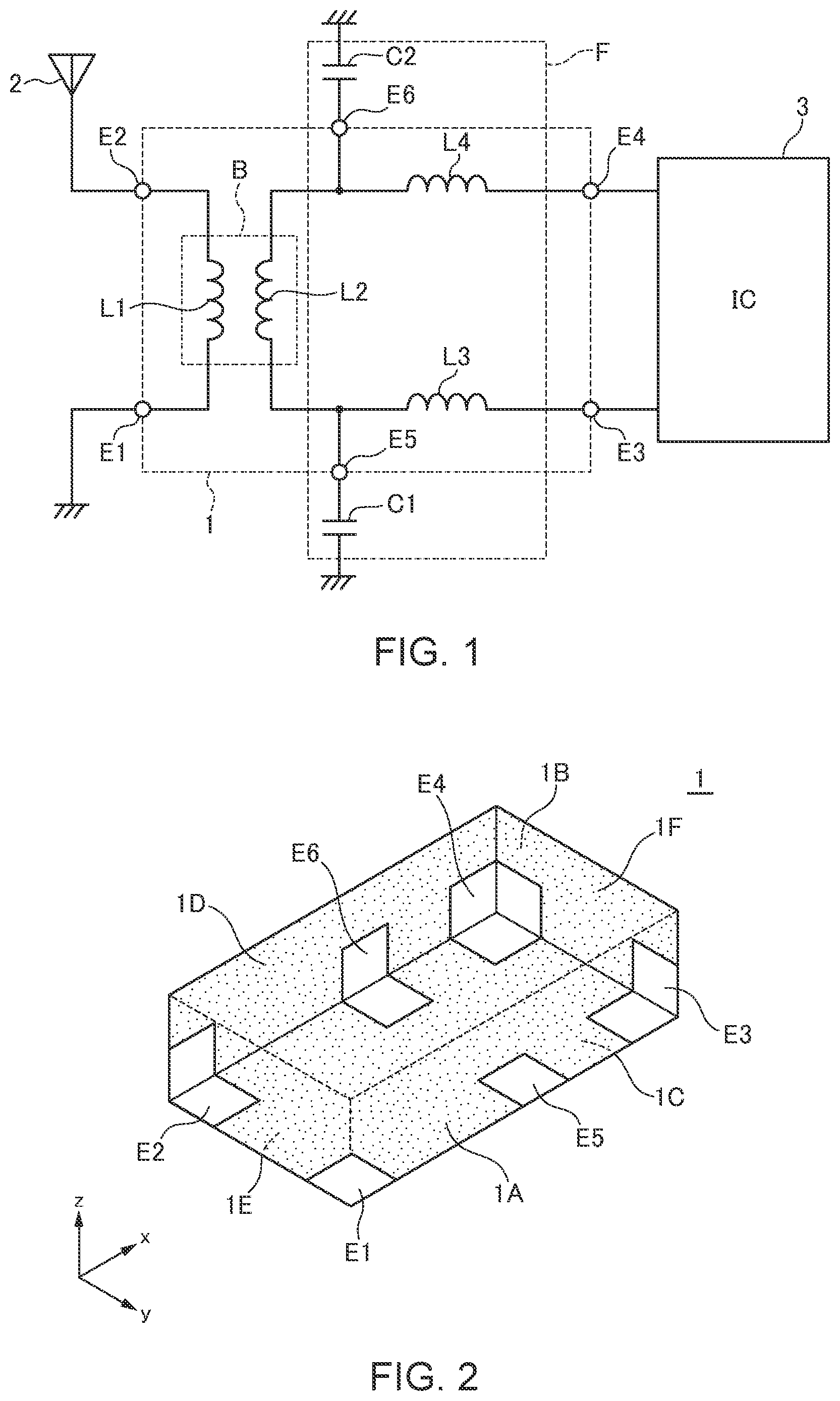
Preferred embodiments of the present invention will now be explained in detail with reference to the drawings. is a circuit diagram of a composite electronic component 1 according to an embodiment of the present invention. As illustrated in , the composite electronic component 1 according to the present embodiment has six terminal electrodes E 1 to E 6 and four inductors L 1 to L 4 . In actual use, the terminal electrode E 1 is grounded, an antenna element 2 is connected to the terminal electrode E 2 , a semiconductor IC 3 is connected to the terminal electrodes E 3 and E 4 , and capacitors C 1 and C 2 are connected respectively between the terminal electrode E 5 and the ground and between the terminal electrode E 6 and the ground. One end of the inductor L 1 is connected to the terminal electrode E 1 and the other end thereof is connected to the terminal electrode E 2 . One end of the inductor L 2 is connected to the terminal electrode E 5 and the other end thereof is connected to the terminal electrode E 6 . One end of the inductor L 3 is connected to the terminal electrode E 5 (one end of the inductor L 2 ) and the other end thereof is connected to the terminal electrode E 3 . One end of the inductor L 4 is connected to the terminal electrode E 6 (the other end of the inductor L 2 ) and the other end thereof is connected to the terminal electrode E 4 . The inductors L 1 and L 2 are magnetically coupled to each other to function as a balun transformer B. The inductors L 3 , L 4 and capacitors C 1 , C 2 function as a low-pass filter F. Thus, an unbalanced signal received by the antenna element 2 is converted into a balanced signal by the balun transformer B, subjected to removal of an unnecessary high-frequency component by the low-pass filter F, and input to the semiconductor IC 3 . is a schematic perspective view illustrating the outer appearance of the composite electronic component 1 according to the present embodiment. As illustrated in , the composite electronic component 1 according to the present embodiment is a surface-mountable single chip component and has a mounting surface 1 A and a top surface 1 B which constitute the xy plane and are positioned opposite to each other, side surfaces 1 C and 1 D which constitute the xz plane and are positioned opposite to each other, and side surfaces 1 E and 1 F which constitute the yz plane and are positioned opposite to each other. The terminal electrodes E 1 to E 6 are exposed to the mounting surface 1 A, the terminal electrodes E 1 , E 3 , and E 5 are exposed to the side surface 1 C, the terminal electrodes E 2 , E 4 , and E 6 are exposed to the side surface 1 D, the terminal electrodes E 1 and E 2 are exposed to the side surface 1 E, and the terminal electrodes E 3 and E 4 are exposed to the side surface 1 F. In actual use, the mounting surface 1 A is mounted so as to face a circuit board. is a schematic exploded perspective view for explaining the internal structure of the composite electronic component 1 according to the present embodiment. is a schematic cross-sectional view taken along the line A-A in , and is a schematic cross-sectional view taken along the line B-B in . As illustrated in to 5 , the composite electronic component 1 according to the present embodiment has four conductor layers 10 , 20 , 30 , and 40 which are stacked in the z-direction. The inductor L 1 is constituted of coil patterns CP 12 and CP 14 formed respectively in the conductor layers 20 and 40 , the inductor L 2 is constituted of coil patterns CP 21 and CP 23 formed respectively in the conductor layers 10 and 30 , the inductor L 3 is constituted of coil patterns CP 31 to CP 34 formed respectively in the conductor layers 10 , 20 , 30 , and 40 , and the inductor L 4 is constituted of coil patterns CP 41 to CP 44 formed respectively in the conductor layers 10 , 20 , 30 , and 40 . The coil patterns CP 21 , CP 12 , CP 23 , and CP 14 constituting the inductors L 1 and L 2 are arranged to overlap one another, the coil patterns CP 31 to CP 34 constituting the inductor L 3 are arranged to overlap one another, and the coil patterns CP 41 to CP 44 constituting the inductor L 4 are arranged to overlap one another. The coil patterns CP 31 to CP 34 constituting the inductor L 3 and the coil patterns CP 41 to 44 constituting the inductor L 4 are smaller in diameter than the coil patterns CP 21 , CP 12 , CP 23 , and CP 14 constituting the inductors L 1 and L 2 . Specifically, the diameter of the inductors L 3 and L 4 is half or less of the diameter of the inductors L 1 and L 2 . A group of the coil patterns CP 31 to CP 34 and a group of the coil patterns CP 41 to CP 44 are arranged in the y-direction, and a group of the coil patterns CP 21 , CP 12 , CP 23 , and CP 14 and a group of the coil patterns CP 31 to CP 34 and CP 41 to CP 44 are arranged in the x-direction. With this configuration, the planar size of the composite electronic component 1 is reduced. Further, the coil patterns CP 31 to CP 34 and the coil patterns CP 41 to CP 44 are symmetric in planar shape with respect to a virtual line X 1 extending in the x-direction. As a result, the coil patterns CP 31 to CP 34 and the coil patterns CP 41 to CP 44 substantially coincide with each other in characteristics. The coil patterns are covered with a magnetic element body M as an exterior body through an insulating layer D made of a resin material. The magnetic element body M is made of a magnetic material obtained by dispersing magnetic fillers in a resin material. The magnetic element body M includes a magnetic layer M 1 covering the coil patterns from one side in the z-direction and constituting the top surface 1 B, a magnetic layer M 2 covering the coil patterns from the other side in the z-direction and constituting the mounting surface 1 A, a magnetic pillar M 3 embedded in the inner diameter areas of the coil patterns CP 21 , CP 12 , CP 23 , and CP 14 and magnetically connecting the magnetic layers M 1 and M 2 , a magnetic shield M 4 provided between the section constituted by the coil patterns CP 21 , CP 12 , CP 23 , CP 14 and the section constituted by the coil patterns CP 31 to CP 34 and CP 41 to CP 44 and magnetically connecting the magnetic layers M 1 and M 2 , and a magnetic layer M 5 constituting the side surfaces 1 C to 1 F. On the other hand, the inner diameter area of the coil patterns CP 31 to CP 34 and the inner diameter area of the coil patterns CP 41 to CP 44 are not provided with the magnetic element body M but are filled with the insulating layer D which is a nonmagnetic material. The magnetic layers M 1 , M 2 , M 5 , the magnetic pillar M 3 , and the magnetic shield M 4 function as a magnetic path for a magnetic field generated from the coil patterns CP 21 , CP 12 , CP 23 , and CP 14 (inductors L 1 and L 2 ). This increases the inductances of the inductors L 1 and L 2 . Further, the magnetic shield M 4 has a role of reducing mutual magnetic interference between the section constituted by the coil patterns CP 21 , CP 12 , CP 23 , and CP 14 (inductors L 1 and L 2 ) and the section constituted by the coil patterns CP 31 to CP 34 (inductor L 3 ) and coil patterns CP 41 to CP 44 (inductor L 4 ). Furthermore, the inductors L 3 and L 4 are covered with the magnetic layers M 1 and M 2 respectively from both sides in the z-direction, covered with the magnetic layer M 5 from both sides in the y-direction, and covered with the magnetic shield M 4 and magnetic layer M 5 respectively from both sides in the x-direction, whereby the influence of external noise is reduced. Further, the inductors L 3 and L 4 each constitute an air-core coil whose inner diameter area is filled with the insulating layer D which is a nonmagnetic material, thus preventing magnetic saturation. to 9 are schematic plan views for explaining the pattern shapes of the conductor layers 10 , 20 , 30 , and 40 , respectively. As illustrated in , the conductor layer 10 has the coil patterns CP 21 , CP 31 , and CP 41 and the terminal electrodes E 1 to E 6 . The outer peripheral ends of the coil patterns CP 21 and CP 41 are connected to the terminal electrode E 6 , and the outer peripheral end of the coil pattern CP 31 is connected to the terminal electrode E 5 . The winding direction from the outer peripheral end to the inner peripheral end is the counterclockwise direction in the coil patterns CP 21 and CP 31 and the clockwise direction in the coil pattern CP 41 . The inner diameter area of the coil pattern CP 21 includes a part of the magnetic pillar M 3 , and the area between the coil pattern CP 21 and the coil patterns CP 31 , CP 41 includes a part of the magnetic shield M 4 . Further, the area between the terminal electrodes adjacent in the x-direction or y-direction includes a part of the magnetic layer M 5 . As illustrated in , the terminal electrode E 6 positioned in the conductor layer 10 may be divided into a part connected to the coil pattern CP 21 and a part connected to the coil pattern CP 41 . The terminal electrode E 5 positioned in the conductor layer 10 may also be divided into two. As illustrated in , the conductor layer 20 has the coil patterns CP 12 , CP 32 , and CP 42 and the terminal electrodes E 1 to E 6 . The outer peripheral end of the coil pattern CP 12 is connected to the terminal electrode E 2 , the inner peripheral end of the coil pattern CP 32 is connected to the inner peripheral end of the coil pattern CP 32 , and the inner peripheral end of the coil pattern CP 42 is connected to the inner peripheral end of the coil pattern CP 41 . The winding direction from the outer peripheral end to the inner peripheral end is the clockwise direction in the coil patterns CP 12 and CP 32 and the counterclockwise direction in the coil pattern 42 . The inner diameter area of the coil pattern CP 12 includes a part of the magnetic pillar M 3 , and the area between the coil pattern CP 12 and the coil patterns CP 32 , CP 42 includes a part of the magnetic shield M 4 . Further, the area between the terminal electrodes adjacent in the x-direction or y-direction includes a part of the magnetic layer M 5 . As illustrated in , the terminal electrodes E 5 and E 6 positioned in the conductor layer 20 may each be divided into two. As illustrated in , the conductor layer 30 has the coil patterns CP 23 , CP 33 , and CP 43 and the terminal electrodes E 1 to E 6 . The outer peripheral end of the coil pattern CP 23 is connected to the terminal electrode E 5 , the inner peripheral end of the coil pattern CP 23 is connected to the inner peripheral end of the coil pattern CP 21 , the inner peripheral end of the coil pattern CP 33 is connected to the inner peripheral end of the coil pattern CP 32 , and the inner peripheral end of the coil pattern CP 43 is connected to the inner peripheral end of the coil pattern CP 42 . The winding direction from the outer peripheral end to the inner peripheral end is the clockwise direction in the coil patterns CP 23 and CP 43 and the counterclockwise direction in the coil pattern 33 . The inner diameter area of the coil pattern CP 23 includes a part of the magnetic pillar M 3 , and the area between the coil pattern CP 23 and the coil patterns CP 33 , CP 43 includes a part of the magnetic shield M 4 . Further, the area between the terminal electrodes adjacent in the x-direction or y-direction includes a part of the magnetic layer M 5 . As illustrated in , the terminal electrodes E 5 and E 6 positioned in the conductor layer 30 may each be divided into two. As illustrated in , the conductor layer 40 has the coil patterns CP 14 , CP 34 , and CP 44 and the terminal electrodes E 1 to E 6 . The outer peripheral end of the coil pattern CP 14 is connected to the terminal electrode E 1 , the inner peripheral end of the coil pattern CP 14 is connected to the inner peripheral end of the coil pattern CP 12 , the outer peripheral end of the coil pattern CP 34 is connected to the terminal electrode E 3 , the inner peripheral end of the coil pattern CP 34 is connected to the inner peripheral end of the coil pattern CP 33 , the outer peripheral end of the coil pattern CP 44 is connected to the terminal electrode E 4 , and the inner peripheral end of the coil pattern CP 44 is connected to the inner peripheral end of the coil pattern CP 43 . The winding direction from the outer peripheral end to the inner peripheral end is the counterclockwise direction in the coil patterns CP 14 and CP 44 and the clockwise direction in the coil pattern 34 . The inner diameter area of the coil pattern CP 14 includes a part of the magnetic pillar M 3 , and the area between the coil pattern CP 14 and the coil patterns CP 34 , CP 44 includes a part of the magnetic shield M 4 . Further, the area between the terminal electrodes adjacent in the x-direction or y-direction includes a part of the magnetic layer M 5 . As illustrated in , the terminal electrodes E 5 and E 6 positioned in the conductor layer 40 may each be divided into two. With the above configuration, the winding direction (counterclockwise direction) of the coil patterns CP 14 and CP 12 starting from the terminal electrode E 1 and the winding direction (clockwise direction) of the coil patterns CP 23 and CP 21 starting from the terminal electrode E 5 are opposite to each other. Further, the winding direction (clockwise direction) of the coil patterns CP 31 to CP 34 starting from the terminal electrode E 3 and the winding direction (counterclockwise direction) of the coil patterns CP 41 to CP 44 starting from the terminal electrode E 4 are opposite to each other. Thus, when current flows from the terminal electrode E 2 toward the terminal electrode E 1 , the current flows from the terminal electrode E 4 toward the terminal electrode E 3 due to magnetic coupling between the inductors L 1 and L 2 constituting the balun transformer B, and an unbalanced signal is converted into a balanced signal. At this time, the direction of the current and the layout of the terminal electrodes on the unbalanced side (input side) coincide with those on the balanced side (output side), so that it is possible to simplify the layout of winding patterns on a substrate mounting the composite electronic component 1 according to the present embodiment. When current flows from the terminal electrode E 4 toward the terminal electrode E 3 , the direction of a magnetic field generated in the inner diameter areas of the coil patterns CP 31 to CP 34 constituting the inductor L 3 and the direction of a magnetic field generated in the inner diameter areas of the coil patterns CP 41 to CP 44 constituting the inductor L 4 coincide with each other. Thus, the magnetic field from the inductor L 3 and the magnetic field from the inductor L 4 cancel each other, reducing magnetic coupling between the inductors L 3 and L 4 , which in turn reduces mutual interference between the inductors L 3 and L 4 . As described above, in the composite electronic component 1 according to the present embodiment, the coil patterns CP 21 , CP 12 , CP 23 , and CP 14 (inductors L 1 and L 2 ) functioning as the balun transformer B and the coil patterns CP 31 to CP 34 (inductor L 3 ) and coil patterns CP 41 to CP 44 (inductor L 4 ) functioning as a part of the low-pass filter F are provided in the same conductor layers, respectively. This makes it possible to reduce the number of conductor layers and to reduce mutual interference between the balun transformer and the inductor. is a schematic perspective view illustrating the outer appearance of a composite electronic component 4 according to a modification. The composite electronic component 4 illustrated in differs from the composite electronic component 1 according to the above embodiment in that the terminal electrodes E 5 and E 6 are exposed not only to the mounting surface 1 A but also to the top surface 1 B. When the terminal electrodes E 5 and E 6 are thus exposed to the top surface 1 B, it is possible to mount a passive component, such as a capacitor, on the top surface 1 B. While the preferred embodiment of the present invention has been described, the present invention is not limited to the above embodiment, and various modifications may be made within the scope of the present invention, and all such modifications are included in the present invention.
Figures (8)
Citations
This patent cites (6)
- US2011/0140806
- US2016/0142031
- US2016/0217917
- US2017/0345551
- US2004304615
- USWO-2014061351