Memory Device Having Load Offset Mismatch Compensation
Abstract
A memory device including a memory cell array which includes a plurality of memory cells connected to each of a plurality of bit lines and word lines, a first bit line sense amplifier electrically connected to a first bit line through a first memory cell and a first connecting wiring and a second bit line sense amplifier electrically connected to a second bit line through a second connecting wiring having a length different from that of the first connecting wiring. A first compensation load of the first bit line and a second compensation load of the second bit line are adjusted to equalize RC loads of the first bit line and the second bit line.
Claims (12)
1 . A memory device comprising: a memory cell array including a plurality of memory cells connected to a plurality of bit lines and a plurality of word lines; a first bit line sense amplifier electrically connected to a first memory cell from among the plurality of memory cells through a first bit line from among the plurality of bit lines and a first connecting wiring having a first length; a first offset compensation transistor electrically connected to the first bit line and the first bit line sense amplifier; a second bit line sense amplifier electrically connected to a second memory cell from among the plurality of memory cells through a second bit line from among the plurality of bit lines and a second connecting wiring having a second length different than the first length; and a second offset compensation transistor electrically connected to the second bit line and the second bit line sense amplifier, wherein the first bit line includes a first compensation load and the second bit line includes a second compensation load to equalize RC loads of the first bit line and the second bit line.
Show 11 dependent claims
2 . The memory device of claim 1 , wherein the first compensation load and the second compensation load are configured to set a ratio of a turn-on resistance of the first offset compensation transistor and a turn-on resistance of the second offset compensation transistor corresponding to a reverse ratio of the first length and the second length.
3 . The memory device of claim 2 , wherein a ratio between a channel width of the first offset compensation transistor and a channel width of the second offset compensation transistor corresponds to the reverse ratio of the first length and the second length.
4 . The memory device of claim 2 , wherein a ratio of a channel length of the first offset compensation transistor and a channel length of the second offset compensation transistor corresponds to a ratio of the first length and the second length.
5 . The memory device of claim 2 , wherein a ratio of channel length per channel width of the first offset compensation transistor to channel length per channel width of the second offset compensation transistor corresponds to the reverse ratio of the first length and the second length.
6 . The memory device of claim 2 , wherein the first bit line sense amplifier is electrically connected to the first memory cell through a first complementary bit line from among the plurality of bit lines, and the second bit line sense amplifier is electrically connected to the second memory cell through a second complementary bit line from among the plurality of bit lines, the memory device further comprising: a first complementary offset compensation transistor electrically connected to the first complementary bit line and the first bit line sense amplifier; and a second complementary offset compensation transistor electrically connected to the second complementary bit line and the second bit line sense amplifier, wherein the first complementary offset compensation transistor has a same turn-on resistance as the second complementary offset compensation transistor.
7 . The memory device of claim 1 , wherein the first bit line sense amplifier further comprises a first switch transistor connected in series to the first offset compensation transistor, and the second bit line sense amplifier comprises a second switch transistor connected in series to the second offset compensation transistor, and wherein the first compensation load and the second compensation load are configured to set a ratio of turn-on resistances of the first switch transistor and the second switch transistor corresponding to a reverse ratio of the first length and the second length.
8 . The memory device of claim 7 , wherein a channel width of the first switch transistor and a channel width of the second switch transistor correspond to a ratio of the first length and the second length.
9 . The memory device of claim 7 , wherein a ratio of a channel length of the first switch transistor to a channel length of the second switch transistor corresponds to the reverse ratio of the first length and the second length.
10 . The memory device of claim 1 , wherein the first bit line sense amplifier further comprises a first compensation transistor connected in series to the first bit line, and the second bit line sense amplifier comprises a second compensation transistor connected in series to the second bit line, and wherein the first compensation load and the second compensation load are configured to set a ratio of turn-on resistances between the first compensation transistor and the second compensation transistor corresponding to a reverse ratio of the first length and the second length.
11 . The memory device of claim 10 , wherein a channel width of the first compensation transistor and a channel width of the second compensation transistor correspond to a ratio of the first length and the second length.
12 . The memory device of claim 10 , wherein a ratio of channel length of the first compensation transistor and channel length of the second compensation transistor corresponds to the reverse ratio of the first length and the second length.
Full Description
Show full text →
CROSS-REFERENCE TO RELATED APPLICATION
(S) This application is based on and claims priority to Korean Patent Application No. 10-2022-0164498, filed on Nov. 30, 2022, in the Korean Intellectual Property Office, the disclosure of which is incorporated by reference herein.
BACKGROUND
The present disclosure relates to memory devices, and more particularly to memory devices including bit line sense amplifiers. Semiconductor memory devices including RAM (Random Access Memory), which is volatile memory, are mainly used as main memory devices of a computer. For example, DRAM (Dynamic Random Access Memory) is a type of volatile RAM made up of memory cells. In order to efficiently sense data stored in the memory cells, a bit line and a complementary bit line are pre-charged with a pre-charge voltage, and then a charge sharing operation is performed to generate a difference between a voltage level of the bit line and a voltage level of the complementary bit line. A bit line sense amplifier senses data stored in a memory cell by amplifying the aforementioned input voltage difference, that is a voltage difference (dVBL) between the bit line and the complementary bit line. Recently, with the development of the electronic industry, there has been increasing demand for high functionality, high speed, and small sized electronic components. Accordingly, to improve the degree of integration of semiconductor memory devices, great effort has been made toward reducing area of the memory cell region, reducing area of peripheral circuitry that is placed adjacent to the memory cell region for driving the memory cells, and increasing the amount of data processing units to speed up data processing. Bit line sense amplifiers may sense and amplify an amount of voltage change of a memory cell. Bit line sense amplifiers typically perform an offset-cancelling operation, a charge-sharing operation, a charge-transfer operation, a sensing operation, and a restore operation, and the offset-cancelling operation is susceptible to affects due to load offset depending on positions of the bit line/complementary bit lines.
SUMMARY
Embodiments of the inventive concepts provide a memory device capable of improving element performance and reliability, and that may evenly adjust a load offset mismatch between the bit lines in a bit line sense amplifier. Embodiments of the inventive concepts provide a memory device having a memory cell array which includes a plurality of memory cells connected to a plurality of bit lines and word lines; a first bit line sense amplifier electrically connected to a first memory cell from among the plurality of memory cells through a first bit line from among the plurality of bot lines and a first connecting wiring having a first length; a first offset compensation transistor electrically connected to the first bit line and the first bit line sense amplifier; a second bit line sense amplifier electrically connected to a second memory cell from among the plurality of memory cells through a second bit line from among the plurality of bit lines and a second connecting wiring having a second length different from the first length; and a second offset compensation transistor electrically connected to the second bit line and the second bit line sense amplifier. The first bit line includes a first compensation load and the second bit line includes a second compensation load to equalize RC loads of the first bit line and the second bit line. Embodiments of the inventive concepts further provide a memory device having a memory cell array including a first memory cell connected between a first bit line node and a first complementary bit line node, and a second memory cell connected between a second bit line node and a second complementary bit line node; a first bit line sense amplifier including a first offset compensation transistor connected between the first bit line node and a first sensing bit line node, and a first complementary offset compensation transistor connected between the first complementary bit line node and a first sensing complementary bit line node; and a second bit line sense amplifier including a second offset compensation transistor connected between the second bit line node and a second sensing bit line node, and a second complementary offset compensation transistor connected between the second complementary bit line node and a second sensing complementary bit line transistor. A first length of a first connecting wiring connecting the first bit line node and one end of the first offset compensation transistor is different from a second length of a second connecting wiring connecting the second bit line node and one end of the second offset compensation transistor. The first bit line includes a first compensation load of the first connecting wiring and the second bit line includes a second compensation load of the second connecting wiring to equalize RC loads of the first connecting wiring and the second connecting wiring. Embodiments of the inventive concepts still further provide a memory device including a memory cell array on a first layer, and including a plurality of memory cells connected between a plurality of bit lines and a plurality of complementary bit lines that are paired; a first offset compensation transistor on a second layer spaced below the first layer, and having one end connected to a first sensing bit line node and an other end connected to a first bit line from among the plurality of bit lines through a first connecting wiring; a first complementary offset compensation transistor on the second layer, and having one end connected to a first complementary sensing bit line node and an other end connected to a first complementary bit line from among the plurality of complementary bit lines through a first complementary connecting wiring having a same length as the first connecting wiring; a second offset compensation transistor on the second layer, and having one end connected to a second sensing bit line node and an other end connected to a second bit line from among the plurality of bit lines through a second connecting wiring having a length different than a length of the first connecting wiring; and a second complementary offset compensation transistor on the second layer, and having one end connected to a second complementary sensing bit line node and an other end connected to a second complementary bit line from among the plurality of complementary bit lines through a second complementary wiring having a same length as the second connecting wiring. One of channel length and channel width of the first offset compensation transistor, or one of channel lengths and channel widths of the second offset compensation transistor and the second complementary offset compensation transistor are set to adjust a first compensation load for the first connecting wiring, and a second compensation load for the second connecting wiring and the second complementary connecting wiring, based on a length ratio of the first connecting wiring and the second connecting wiring.
BRIEF DESCRIPTION OF THE DRAWINGS
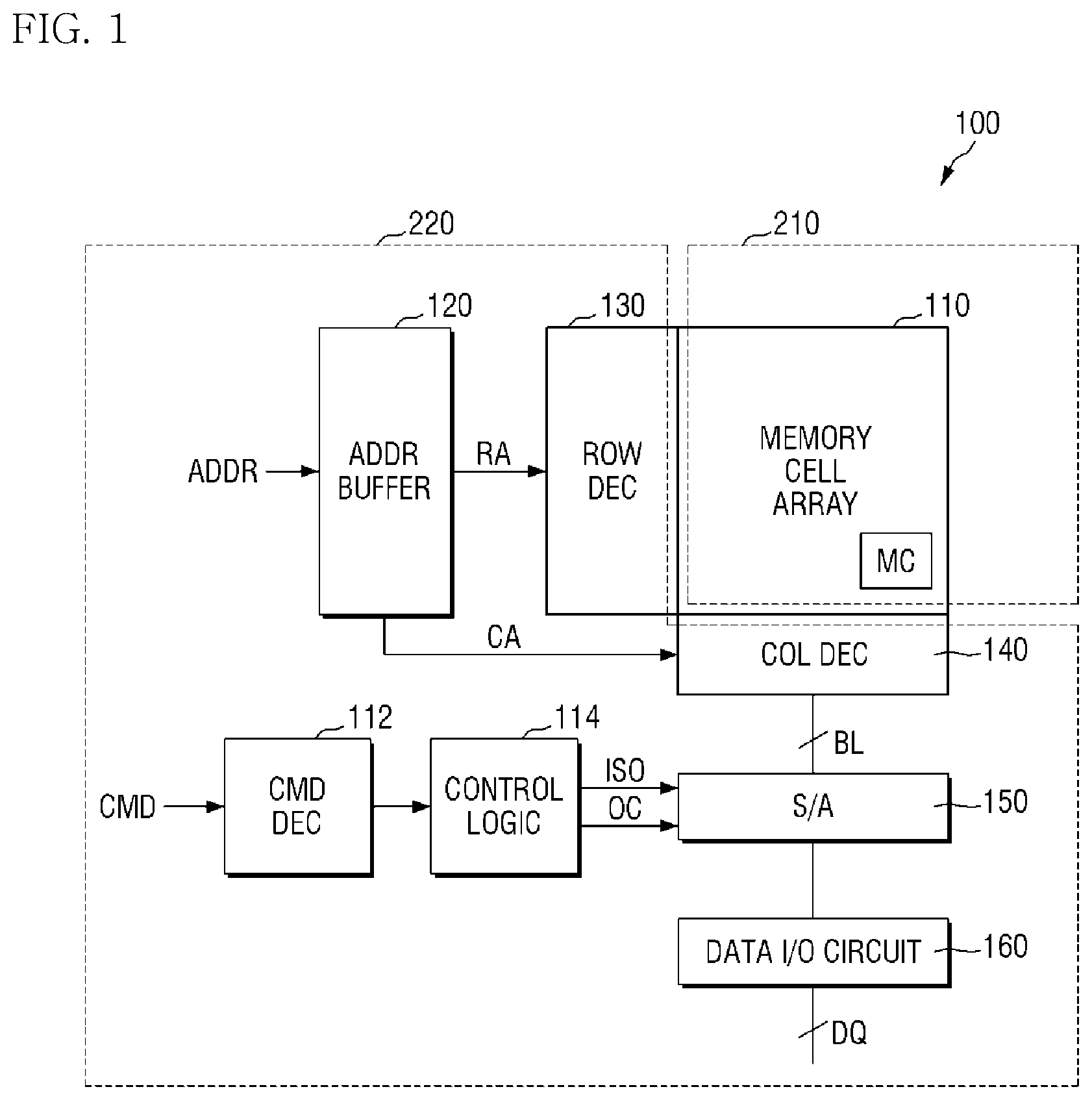
The above and other aspects, features and advantages of the inventive concepts will be more clearly understood from the following detailed description taken in conjunction with the accompanying drawings, in which: illustrates a diagram of a memory device according to embodiments of the inventive concepts. illustrates a diagram of the memory cell of . illustrates a diagram of a memory cell array including bit line sense amplifiers according to embodiments of the inventive concepts. illustrates a conceptual diagram of placement of the memory device according to embodiments of the inventive concepts. illustrates a conceptual diagram explanatory of the second layer 220 of according to embodiments of the inventive concepts. illustrates a circuit diagram of a bit line sense amplifier according to embodiments of the inventive concepts. illustrates a voltage-current graph explanatory of a turn-on resistance that varies depending on the channel length and channel width of a transistor. A illustrates a table explanatory of a channel width of an offset compensation transistor included in the bit line sense amplifier according to embodiments of the inventive concepts. B illustrates a layout diagram of a channel of the offset compensation transistor MN 6 in . A illustrates a table explanatory of a channel length of an offset compensation transistor included in the bit line sense amplifier according to embodiments of the inventive concepts. B illustrates a layout diagram of a channel of the offset compensation transistor MN 6 in . A illustrates a table explanatory of a channel length and a channel width adjusted for an offset compensation transistor included in the bit line sense amplifier according to embodiments of the inventive concepts. B illustrates a layout diagram of a channel of the offset compensation transistor according to A . A and 11 B illustrate circuit diagrams of bit line sense amplifiers according to embodiments of the inventive concepts. illustrate tables explanatory of channel width of a switch transistor included in the bit line sense amplifier according to embodiments of the inventive concepts. illustrates a table explanatory of channel length of the switch transistor included in the bit line sense amplifier according to embodiments of the inventive concepts. illustrates a table explanatory of a ratio of the channel length to the channel width of the switch transistor included in the bit line sense amplifier according to embodiments of the inventive concepts. illustrates a voltage-current graph explanatory of a turn-on resistance change of a transistor according to the gate bias. illustrates a table explanatory of the gate bias setting of a switch transistor included in a bit line sense amplifier according to embodiments of the inventive concepts. A and 18 B illustrate circuit diagrams of bit line sense amplifiers according to embodiments of the inventive concepts. illustrate tables explanatory of a channel width of a compensation transistor included in the bit line sense amplifier according to embodiments of the inventive concepts. illustrates a table explanatory of a channel length of the compensation transistor included in the bit line sense amplifier according to embodiments of the inventive concepts. illustrates a table explanatory of a ratio of the channel length to the channel width of the switch transistor included in the bit line sense amplifier according to embodiments of the inventive concepts. illustrates a table explanatory of gate bias settings of a switch transistor included in the bit line sense amplifier according to embodiments of the inventive concepts. A and 24 B illustrate circuit diagrams of bit line sense amplifiers according to embodiments of the inventive concepts. A and 25 B illustrate circuit diagrams of bit line sense amplifiers according to embodiments of the inventive concepts. A and 26 B illustrate circuit diagrams of bit line sense amplifiers according to embodiments of the inventive concepts.
DETAILED
DESCRIPTION OF THE EMBODIMENTS
Hereinafter, various embodiments will be described with reference to the accompanying drawings. Embodiments may be described and illustrated in terms of blocks which carry out a described function or functions. These blocks, which may be referred to herein as units or modules or the like, are physically and/or electrically implemented by analog and/or digital circuits such as logic gates, integrated circuits, microprocessors, microcontrollers, memory circuits, passive electronic components, active electronic components, optical components, hardwired circuits and the like, and may be driven by firmware and/or software. The circuits may, for example, be embodied in one or more semiconductor chips, or on substrate supports such as printed circuit boards and the like. The circuits constituting a block may be implemented by dedicated hardware, or by a processor (e.g., one or more programmed microprocessors and associated circuitry), or by a combination of dedicated hardware to perform some functions of the block and a processor to perform other functions of the block. Each block of the embodiments may be physically separated into two or more interacting and discrete blocks without departing from the scope of the inventive concepts. Likewise, the blocks of the embodiments may be physically combined into more complex blocks without departing from the scope of the inventive concepts. illustrates a diagram of a memory device according to embodiments of the inventive concepts. Referring to , a memory device 100 may be a storage device based on a semiconductor element. For example, the memory device 100 may include DRAM (Dynamic Random Access Memory) such as a DDR SDRAM (Double Data Rate Static DRAM), a SDR SDRAM (Single Data Rate SDRAM), a LPDDR SDRAM (Low Power DDR SDRAM), a LPSDR SDRAM (Low Power SDR SDRAM), and a Direct RDRAM (Rambus DRAM), or may be an arbitrary volatile memory device. In particular, the memory device 100 may be a device to which standard conventions such as DDR4 or DDR5 are applied. In an embodiment, the number of data pins to which the DDR4 or DDR5 standard conventions are applied may be four, eight or sixteen, and the number of data pins of the semiconductor memory device 100 according to the inventive concepts may be sixteen. The description of the number of data pins of the memory system 50 and the like used in the description herein below may be applied according to the standard conventions of dynamic random access memory, but is not necessarily limited thereto. The memory device 100 may output data through data lines DQ in response to command CMD, address ADDR, and control signals received from an external device, for example, a memory controller. The memory device 100 includes a memory cell array 110 , a command decoder 112 , a control logic (e.g., circuit) 114 , an address buffer 120 , a row decoder 130 , a column decoder 140 , a sense amplifier array (S/A) 150 , and a data input/output (I/O) circuit 160 . The memory cell array 110 includes a plurality of memory cells (MC) provided in the form of a matrix arranged in rows and columns. The memory cell array 110 includes a plurality of word lines and a plurality of bit lines BL connected to the memory cells. The plurality of word lines may be connected to rows of the memory cells, and a plurality of bit lines BL may be connected to columns of the memory cells. According to some embodiments, the memory cells may include a normal memory cell and a redundant memory cell that store data. The redundant memory cell is used to relieve a defective normal memory cell when the normal memory cell becomes defective. The command decoder 112 decodes the command CMD received from the memory controller, which may be for example, a write enable signal (/WE), a row address strobe signal (/RAS), a column address strobe signal (/CAS), a chip select signal (/CS), and the like. The command CMD may include an active command, a read command, a write command, a pre-charge command, and the like. The control logic 114 may generate various control signals necessary for access operation to the memory cell array 110 , for example, the write operation, the read operation, the pre-charge operation, and the like, in response to the decoded command. The address buffer 120 receives the address ADDR from a memory controller, which is an external device. The address ADDR includes a row address RA for addressing a row of the memory cell array 110 , and a column address CA for addressing a column of the memory cell array 110 . The address buffer 120 may transmit the row address RA to the row decoder 130 , and transmit the column address CA to the column decoder 140 . The row decoder 130 may select any one of a plurality of word lines WL connected to the memory cell array 110 . The row decoder 130 may decode the row address RA received from the address buffer 120 , select any one word line corresponding to the row address RA, and activate the selected word line. A high power supply voltage VPP higher than a power supply voltage VDD may be applied to a gate of an access transistor of the memory cell, at the time of activation of the word line, that is, the word line enable operation. The column decoder 140 may select a predetermined bit line among the plurality of bit lines BL of the memory cell array 110 . The column decoder 140 may decode the column address CA received from the address buffer 120 to select a predetermined bit line BL corresponding to the column address CA. The sense amplifier array (S/A) 150 is connected to bit lines BL of the memory cell array 110 . The sense amplifier array 150 senses a voltage change of a bit line selected among the plurality of bit lines BL, amplifies the voltage, and outputs the amplified voltage. The data input/output circuit 160 may output data, which is output on the basis of voltage sensed and amplified by the sense amplifier array 150 , to outside through the data lines DQ. An arbitrary bit line sense amplifier BLSA in the sense amplifier array 150 may be connected to a bit line pair consisting of the first bit line BL and the complementary bit line BLB of the first bit line BL to sense and amplify the potential appearing on the bit lines. A specific connection between the bit line sense amplifier and the bit line pair will be described hereinafter with respect to . The sense amplifier array 150 may receive an isolation signal ISO and an offset removal signal OC from the control logic 114 . The sense amplifier array 150 may perform an offset removal operation according to the isolation signal ISO and the offset removal signal OC. As an example, the offset refers to a difference in characteristics between the semiconductor elements that make up the sense amplifier array 150 , for example, threshold voltages. illustrates a diagram explanatory of the memory cell of . Referring to , the memory cells MC included in the memory cell array are connected to each of the word lines WL and each of the bit lines BL. Although only the bit line BL is shown for convenience of explanation, the memory cell MC is connected to the bit line BL and the complementary bit line BLB. The memory cell MC is made up of a cell transistor MTR and a cell capacitor C. The memory device 100 may perform a read operation or a refresh operation on the basis of the charge amount of the cell capacitor C included in the memory cell MC. For example, the first bit line BL connected to the memory cell MC is pre-charged with a pre-charge voltage Vpre. After that, as the word line WL is activated, a charge sharing operation between the charge of the first bit line BL charged with the pre-charge voltage Vpre and the charge of the cell capacitor C of the memory cell MC occurs. Due to the charge sharing operation, the voltage of the first bit line BL will decrease or increase by the voltage change amount V from the pre-charge voltage Vpre. Each sense amplifier of the sense amplifier array 150 may sense and amplify the voltage change amount V. illustrates a diagram of a memory cell array to which the bit line sense amplifiers according to some embodiments are applied. Referring to , the memory device 100 includes a plurality of memory cell arrays 110 _ 1 to 110 _ n , and a plurality of bit line sense amplifiers 150 _ 1 to 150 _ n. Each of the plurality of bit line sense amplifiers 150 _ 1 to 150 _ n may include a plurality of bit line sense amplifiers (hereafter, referred to as BLSA). The BLSAs may be implemented as the sense amplifier array 150 described with respect to to 3 . A plurality of bit line-complementary bit line pairs (BL-BLB pairs) connected to each of the plurality of memory cell arrays 110 _ 1 to 110 _ n may be connected to each of a plurality of BLSAs. Each BLSA may be a cross-coupled differential sense amplifier implemented as a P-type sense amplifier and an N-type sense amplifier. Each BLSA is a circuit element that normally operates at the time of operation of the semiconductor memory device, and is distinguished from dummy sense amplifiers 150 - 1 and 150 - n implemented in a region other than a region in which the bit line sense amplifiers 150 _ 2 to 150 _ n −1 are implemented. According to some embodiments, the odd bit lines of memory cell array 110 _ 1 may be connected to the first bit line BL, and the even bit lines may be connected to complementary bit line BLB. A BLSA 150 - 2 may be bi-directionally connected to each of the bit line pairs BL and BLB. For example, the BLSA 150 - 2 is connected to odd-numbered bit lines (e.g., BL 1 , BL 3 , BL 5 , . . . etc.) of a left first memory cell array 110 _ 1 , that is, the bit line BL, and the bit line sense amplifier 150 - 2 may be connected to even-numbered bit lines (e.g., BL 0 , BL 2 , BL 4 , . . . etc.) of a right second memory cell array 110 _ 2 , that is, the complementary bit line BLB. When the potential of the bit line BL is a high potential in the sensing operation of BLSA, the potential of the complementary bit line BLB becomes a low potential. On the other hand, when the potential of the bit line BL is a low potential in the sensing operation of BLSA, the potential of the complementary bit line BLB becomes a high potential. Although not shown, the odd-numbered bit lines of the second memory cell array 110 _ 2 may extend in a direction opposite to the BLSA 150 - 2 and be connected to the BLSA 150 - 3 . Although the BLSAs 150 _ 1 to 150 _ n are shown as flat surfaces in , this is for explaining the connections between the memory cell arrays 110 _ 1 , and 110 _ 2 to 110 _ n and the bit line BL or the complementary bit line BLB. According to various embodiments, the BLSA 150 may be placed on the same layer as the memory cell array 110 , or according to other embodiments, the BLSA 150 may be placed on a different layer from the memory cell array 110 along with other logic circuits. illustrates a conceptual diagram of a placement of the memory device according to some embodiments. Referring to , the memory device 100 according to some embodiments may be implemented on a plurality of layers. The first layer 210 and the second layer 220 may be flat surfaces that are vertically spaced apart and parallel to each other. For example, the first layer 210 may be a cell array layer, and the second layer 220 may be a logic layer. According to an embodiment, the memory cell array 110 is placed on the first layer 210 , and the peripheral circuits 120 , 130 , 140 , 150 , 160 , 112 , 114 , and the like for driving the memory cell array 110 may be placed on the second layer 220 . Alternatively, according to an embodiment, the first layer 210 may be placed to include a memory cell array 110 , a row decoder 130 , and a column decoder 140 , and the second layer 220 may be placed to include the remaining peripheral circuits 112 , 114 , 120 , 150 , and 160 . Alternatively, according to an embodiment, the command decoder 112 and the control logic 114 may be placed in separate layers, and the second layer 220 may include the remaining peripheral circuits 120 , 130 , 140 , 150 , and 160 . In the above embodiments, the memory cell MC of the first layer 210 is connected to the bit line BL and the complementary bit line BLB, and the bit line/complementary bit line BL/BLB is connected to the bit line sense amplifier 150 located on the second layer 220 . However, a load offset of the bit line/complementary bit line BL/BLB may occur depending on the position of the memory cell. illustrates a conceptual diagram explanatory of the second layer 220 of according to some embodiments. may be characterized as a top plan view of the second layer 220 which is planar and extends along an X-direction and a Y-direction that is perpendicular to the X-direction. Referring to , 4 and 5 , the second layer 220 may include peripheral circuits for driving the memory cell array 110 . According to some embodiments, the second layer 220 may include sense amplifier regions 221 - 1 and 221 - 2 , and peripheral circuitry regions 223 - 1 and 223 - 2 . A plurality of bit line sense amplifiers 150 connected to each of the bit line BL and the complementary bit line BLB to sense and amplify the voltage change amount of memory cell MC may be placed in the sense amplifier regions 222 - 1 and 221 - 2 . The peripheral circuit regions 223 - 1 and 223 - 2 may include remaining peripheral circuit configurations (e.g., 120 , 130 , 140 , 160 , etc.) of the peripheral circuits of other than the bit line sense amplifier. According to some embodiments, the second layer 220 may include a plurality of sense amplifier regions 221 - 1 and 221 - 2 , and a plurality of peripheral circuit regions 223 - 1 and 223 - 2 . In the shown example, although the second layer 220 will be described as including two sense amplifier regions 221 - 1 and 221 - 2 and two peripheral circuit regions 223 - 1 and 223 - 2 , the embodiments of the inventive concepts are not limited thereto. The memory cell array of the first layer 210 may be placed by being divided into sub-arrays. For example, a first sub-array is placed at a position corresponding to the sense amplifier region 221 - 1 and the peripheral circuit region 223 - 1 , and a second sub-array may be placed at a position corresponding to the sense amplifier region 221 - 2 and the peripheral circuit region 223 - 2 . The sense amplifier regions 221 - 1 and 221 - 2 and the peripheral circuit regions 223 - 1 and 223 - 2 may be placed point-symmetrically. For example, the sense amplifier region 221 - 1 and the peripheral circuit region 223 - 1 are placed in the first row, and the peripheral circuit region 223 - 2 and the sense amplifier region 221 - 2 may be placed in the second row. The sense amplifier regions 221 - 1 and 221 - 2 may be placed point-symmetrically to each other, and the peripheral circuit regions 223 - 1 and 223 - 2 may be placed point-symmetrically to each other. The sense amplifier region 221 - 1 includes a plurality of connecting bit line wirings A 1 , B 1 , C 1 and D 1 , and the connecting bit line wirings A 1 , B 1 , C 1 and D 1 are spaced apart from each other and placed parallel in the Y-direction, while extending in the X-direction. The peripheral circuit region 223 - 1 includes connecting signal wirings A 3 , B 3 , C 3 and D 3 , and the connecting signal wirings A 3 , B 3 , C 3 and D 3 are spaced apart from each other and placed parallel in the Y-direction, while extending in the X-direction. According to some embodiments, the connecting bit line wiring and the connecting signal wiring may be placed on the same axis extending in the X-direction. For example, the connecting bit line wiring A 1 and the connecting signal wiring A 3 may be placed on a same X axis, while being spaced apart from each other. The connecting regions TA, TB, TC, and TD include a plurality of through channels, and the through channels independently send the bit line/complementary bit line (BL/BLB) signal, the word line signal, the control signal, and the like. The connecting regions TA, TB, TC, and TD may connect the connecting bit lines A 1 , B 1 , C 1 , and D 1 and the bit line/complementary bit line BL/BLB of the memory cells of the first layer 210 . The connecting regions TA, TB, TC, and TD may be connected to the connecting signal wirings A 3 , B 3 , C 3 , and D 3 of the peripheral circuit region 223 - 1 through the connecting wirings A 2 , B 2 , C 2 , and D 2 . The connecting regions TA, TB, TC, and TD may be placed inside the sense amplifier region 221 - 1 alternately both in the X-direction and the Y-direction. That is, they may be placed on different Y-axes in the Y-direction, while being placed on different X-axes in the X-direction. For example, the connecting regions TA, TB, TC, and TD may be placed diagonally from a planar viewpoint such that the connecting wirings A 2 , B 2 , C 2 , and D 2 become increasingly longer or gradually shorter. Further, for example, the connecting regions TA, TB, TC, and TD may be placed in a U shape (or reversed U shape) from a planar viewpoint in which the connecting wirings A 2 , B 2 , C 2 , and D 2 become longer and shorter, or become shorter and longer. That is, the connecting bit line wirings A 1 , B 1 , C 1 , and D 1 and the connecting wirings A 3 , B 3 , C 3 , and D 3 have the same length in the respective regions 221 - 1 and 223 - 1 , but the connecting wirings A 2 , B 2 , C 2 and D 2 have different wiring lengths corresponding to the connecting regions TA, TB, TC and TD. The bit line sense amplifiers 150 thus have a load offset corresponding to the lengths of the connecting wirings A 2 , B 2 , C 2 and D 2 . The load offset means that an RC load (Resistive Capacitive Load, hereinafter an RC load) varies depending on the length of the connecting wiring connected between the bit line BL of the memory cell and a bit line sense amplifier 150 , for example. In the shown example, the RC load of the connecting wiring A 2 may have a different value from the RC load of the connecting wiring D 2 . A RC load offset mismatch of the bit line/complementary bit line according to the length of the connecting wiring may affect the offset canceling operation of the bit line sense amplifier 150 . illustrates a circuit diagram of a bit line sense amplifier according to some embodiments. The bit line sense amplifier 10 of may be an embodiment of the bit line sense amplifier 150 of . Referring to , the BLSA 10 according to some embodiments may include amplification transistors MP 1 , MP 2 , MN 1 , and MN 2 , isolation transistors MN 3 and MN 4 , offset compensation transistors MN 5 and MN 6 , and an equalizing enable transistor MP 7 . The amplification transistors MP 1 , MP 2 , MN 1 , and MN 2 are connected between a first supply line (LA, N 1 ) supplied with a first control signal LA and a second supply line (LAB, N 2 ) supplied with a second control signal LAB. For example, a P-type amplification transistor MP 1 and an N-type amplification transistor MN 1 are connected in series between the first supply line N 1 and the second supply line N 2 , and a P-type amplification transistor MP 2 and an N-type amplification transistor MN 2 are connected in series between the first supply line N 1 and the second supply line N 2 . Drain terminals of the P-type amplification transistor MP 1 and the N-type amplification transistor MN 1 are commonly connected to a sensing bit line node N 3 , and drain terminals of the P-type amplification transistor MP 2 and the N-type amplification transistor MN 2 are commonly connected to a complementary sensing bit line node N 4 . The N 3 node may be called a complementary sensing bit line node SBLB, and the N 4 node may be called a sensing bit line node SBL. The P-type transistor MP 1 and the P-type transistor MP 2 are cross-coupled, and gate terminals are connected to drain terminals (the gate of MP 1 is connected to the N 4 node, and the gate of MP 2 is connected to the N 3 node). The N-type transistor MN 1 and the N-type transistor MN 2 are cross-coupled, and gate terminals are connected to drain terminals (the gate of MN 1 is connected to the N 4 node through N-type isolation transistor MN 3 , and the gate of MN 2 is connected to the N 3 node through N-type isolation transistor MN 4 ). On the other hand, the gate of the N-type amplification transistor MN 1 is connected to a bit line node N 5 connected to the bit line BL of the memory cell, and the gate of the N-type amplification transistor MN 2 is connected to a complementary bit line node N 6 connected to a complementary bit line BLB of the memory cell. The isolation transistor MN 3 is connected between the N 5 node and the N 4 node to connect or disconnect the bit line BL and the sensing bit line SBL depending on the isolation control signal P 2 . The isolation transistor MN 4 is connected between the N 6 node and the N 3 node to connect or disconnect the complementary bit line BLB and the complementary sensing bit line SBLB depending on the isolation control signal P 2 . According to some embodiments, the BLSA 10 includes an equalizing enable transistor MP 7 . The equalizing enable transistor MP 7 is connected to the sensing bit line node N 3 according to the equalizing control signal PEQ, and pre-charges the sensing bit line SBL with an equalizing voltage. According to some embodiments, the BLSA 10 includes offset compensation transistors MN 5 and MN 6 . The offset compensation transistors MN 5 and MN 6 remove an offset generated between the bit line BL and the complementary sensing bit line SBLB, or between the complementary bit line BLB and the sensing bit line SBL. The offset compensation transistor is also called an offset removal transistor. The offset compensation transistor MN 5 is connected between the bit line node N 5 and the complementary sensing bit line node N 3 to connect or disconnect the bit line BL and the complementary sensing bit line SBLB to each other depending on the offset control signal P 1 . The offset compensation transistor MN 6 is connected between the complementary bit line node N 6 and the sensing bit line node N 4 to connect or disconnect the complementary bit line BLB and the sensing bit line SBL to each other depending on the offset control signal P 1 . The BLSA 10 according to some embodiments may further include a level balancing transistor MN 8 . The level balancing transistor MN 8 may be turned on during the pre-charge operation to set the node N 3 and the node N 4 to the same level so that a threshold voltage Vth difference between the transistors MP 1 and MP 2 does not occur in the pre-charge operation. The bit line BL may have a parasitic resistance Rb 1 and a parasitic capacitor Cb 1 of the bit line itself. The parasitic resistance Rb 1 and the parasitic capacitor Cb 1 are depicted as connected to each other at node N 7 . The complementary bit line BLB may also have parasitic resistances Rb 1 and Rbp and parasitic capacitors Cb 1 and Cbp of the complementary bit line itself connected to nodes N 8 and N 9 . However, as explained above, depending on the position of BLSA 10 on the layer 220 , the lengths of the connecting wirings (A 2 , B 2 , C 2 , and D 2 of ) to the N 5 and N 6 nodes of the BLSA 10 vary (i.e., may be different). Accordingly, the RC loads (Rb 1 , Cb 1 ) of the bit line BL itself and the RC loads (Rb 1 +Rbp, Cb 1 +Cbp) of the complementary bit line BLB itself may differ by an additional parasitic resistance Rbp and an additional parasitic capacitor Cbp depending on the connecting wiring length. That is, the BLSA 10 may be connected by connecting wirings having lengths different from those of the memory cell array, on the bit line side and the complementary bit line side. For example, the bit line may be connected by a short connecting wiring and the complementary bit line may be connected by a long connecting wiring, or conversely, the bit line may be connected by a long connecting wiring and the complementary bit line may be connected by a short connecting wiring. When the connecting wirings of different lengths are connected to the bit line and the complementary bit line, the extent of a parasitic resistance or a parasitic capacitor may affect differential sensing of the BLSA 10 . Referring to , according to some embodiments, it is assumed that the bit lines BL (e.g., A 1 , B 1 , C 1 and D 1 ) have the same length, and the complementary bit lines BLB have different connecting wiring lengths for each region. It is assumed that among the plurality of BLSAs 10 , the BLSA of the connecting region TA has the shortest connecting wiring length (e.g., A 2 ), the BLSA of the connecting region TD has the longest connecting wiring length (e.g., D 2 ), and the connecting wiring lengths increase at a rate of A 2 :B 2 :C 2 :D 2 =1:2:3:4. Accordingly, when there is no additional compensation load for each bit line, the RC load may increase in order of A 2 , B 2 , C 2 , and D 2 . In , it is assumed that the offset transistor MN 5 included in the BLSA 10 has a channel width of Woc 1 and a channel length of Loc 1 , and the offset transistor MN 6 has a channel width of Woc 2 and a channel length of Loc 2 . For convenience of explanation, although a case where the connecting wiring length of the complementary bit line BLB is different will be described, the embodiments of the inventive concepts may also be similarly applied to a case where the connecting wiring length of the bit line BL is different for each region. The memory device may further include a compensation load for each BLSA 10 to prevent an RC load offset mismatch regardless of the position of the corresponding BSLA 10 . A compensation load adjustment of the memory device according to various embodiments will described below with reference to to 26 A . For example, a first bit line includes a first compensation load of the first connecting wiring and a second bit line includes a second compensation load of the second connecting wiring. The first compensation load and the second compensation load provide to remove a RC load offset to equalize RC loads of the first connecting wiring and the second connecting wiring. illustrates a voltage-current graph explanatory of that a turn-on resistance varies depending on the channel length and channel width of a transistor. The horizontal X-axis represents drain-source voltage (Vds) of a transistor, and the vertical Y-axis represents drain current (Id) of the transistor. Referring to , the transistor may be adjusted in channel width and/or channel length to adjust the turn-on resistance value. A turn-on resistance value R of a transistor is inversely proportional (i.e., R ∝L/A) to the channel cross-sectional area A, and proportional to the channel length L. Since the channel width W is proportional to the cross-sectional area, the turn-on resistance value is inversely proportional to the channel width. When adjusting the channel length of a transistor, adjusting the channel width, or adjusting the ratio of channel length to channel width at the time of designing a memory device according to such a relationship, a turn-on resistance value may be adjusted from R to R′ according to the voltage-current graph of the transistor. According to some embodiments, the turn-on resistance of the offset compensation transistors MN 5 and MN 6 of the memory device may be adjusted to adjust for the compensation load. For example, the compensation load may be adjusted by adjusting the channel widths, adjusting the channel length, or adjusting the ratio of channel width to channel length of the offset compensation transistors MN 5 and MN 6 . A to 10 B are embodiments for adjusting the turn-on resistance of the offset compensation transistor. A illustrates a table explanatory of a channel width of the offset compensation transistor included in the bit line sense amplifier according to some embodiments, and B illustrates a layout diagram that simply shows a channel of the offset compensation transistor (e.g., MN 6 in A ). For example, referring to to 8 A , at the connecting regions TA, TB, TC and TD, the channel widths Woc 1 of the offset compensation transistors MN 5 of the BLSAs have a ratio of 1:1:1:1. That is, the channel width is Woc for the offset compensation transistors MN 5 of the BLSA 10 in each of connecting region TA, connecting region TB, connecting region TC, and connecting region TD. Each of the offset compensation transistors MN 5 of the BLSAs in connecting regions TA, TB, TC and TD have a 40 kohm turn-on resistance value (Roc 1 ). That is, in this example embodiment, the offset compensation transistor MN 5 of the BLSAs in each connecting region has the same channel width and the same turn-on resistance regardless of the BLSA position. On the other hand, in the connecting regions TA, TB, TC and TD, the channel widths Woc 2 of the offset transistors MN 6 of the BLSAs have a ratio of 1:1.3:2:4. That is, the channel width Woc 2 of the offset compensation transistor MN 6 in connecting region TA is Woc, the channel width Woc 2 of the offset compensation transistor MN 6 in connecting region TB is (1.3×Woc), the channel width Woc 2 of the offset compensation transistor MN 6 in connecting region TC is (2×Woc), and the channel width Woc 2 of the offset compensation transistor MN 6 in connecting region TD is (4×Woc), in consideration of the difference in complementary connecting wiring lengths (e.g., A 2 , B 2 , C 2 , and D 2 of ). Because of the difference in the channel widths Woc 2 , the turn-on resistance values Roc 2 of the offset compensation transistors MN 6 in the connecting regions TA, TB, TC and TD of the BLSAs are respectively 40 kohm, 30 kohm, 20 kohm, and 10 kohm. That is, the length of the complementary connecting wirings according to the BLSA positions have a ratio of 1:2:3:4, whereas the turn-on resistance values Roc 2 have a ratio of 4:3:2:1 so that a RC load, which is the sum of the parasitic loads (Rbp, Cbp) of the complementary connecting wiring and the compensation load Roc due to the offset compensation transistor, is made uniform. In other words, the offset compensation transistor MN 6 has a turn-on resistance value Roc 2 according to the reverse ratio of the connecting wiring length ratio. The offset compensation transistor MN 6 may be designed as in B according to the channel width ratio of A . Referring to B , in the offset compensation transistor MN 6 , a gate poly (indicated as gp in B ) extending along the Y-direction while partially overlapping the active regions is placed on a pair of active regions which extend in the Y-direction and which are spaced apart from each other in the X-direction, and small square direct contacts (indicated as dc in B ) are placed on each side of the gate poly on different X-axes. The direct contacts may be source/drain contacts that are each electrically connected to the active region. A channel width (indicated as a in B ) may be defined as a longer length (a length in the Y-direction as shown) on the basis of the direct contacts in the gate poly layer, and an area formed as the channel due to the active region pair below the gate poly layer. For example, the channel width Woc 2 of the offset compensation transistor MN 6 of the BLSA in the connecting region TA may be set as 1 a , the channel width Woc 2 of the offset compensation transistor MN 6 of the BLSA in the connecting region TB may be set as 1 . 3 a , the channel width Woc 2 of the offset compensation transistor MN 6 of the BLSA in the connecting region TC may be set as 2 a , and the channel width Woc 2 of the offset compensation transistor MN 6 of the BLSA in the connecting region TD may be set as 4 a. A illustrates a table explanatory of a channel length of the offset compensation transistor included in the bit line sense amplifier according to some embodiments, and B is a layout diagram that simply shows the channel of the offset compensation transistor MN 6 of A . For example, referring to A , for the connecting regions TA, TB, TC and TD, the channel lengths Loc 1 of the offset compensation transistors MN 5 of the BLSAs have a ratio of 1:1:1:1. That is, the channel length Loc 1 for the offset compensation transistors MN 5 in each of connecting regions TA, TB, TC and TD is (4×Loc), and the turn-on resistance value Roc 1 of the offset compensation transistors MN 5 in each of the connecting regions TA, TB, TC and TD is 40 kohm. That is, in this example embodiment, the offset compensation transistors MN 5 of the BLSAs in each connecting region have the same channel length and have the same turn-on resistance regardless of the BLSA position. On the other hand, as shown in A , in the connecting regions TA, TB, TC and TD, the turn-on resistance values Roc 2 of the offset compensation transistors MN 6 of the BLSAs are respectively 40 kohm, 30 kohm, 20 kohm, and 10 kohm, as a compensation load. For example, the channel lengths Loc 2 of the offset transistors MN 6 have a ratio of 4:3:2:1. That is, the channel length Loc 2 of the offset compensation transistor MN 6 in the connecting region TA is (4×Loc), the channel length Loc 2 of the offset compensation transistor MN 6 in the connecting region TB is (3×Loc), the channel length Loc 2 of the offset compensation transistor MN 6 in the connecting region TC is (2×Loc), and the channel length Loc 2 of the offset compensation transistor MN 6 in the connecting region TD is (Loc), in consideration of a difference in complementary connecting wiring lengths (e.g., A 2 , B 2 , C 2 , and D 2 of ). Since the resistance value R is proportional to the wiring length L according to the difference in the channel length Loc 2 , the ratio of the channel lengths Loc 2 may be set to correspond to the reverse number and reverse ratio (Loc A :Loc B :Loc C :Loc D = 1/1:½:⅓:¼=4:3:2:1) of the ratio of the turn-on resistance value, that is, the ratio (A 2 :B 2 :C 2 :D 2 =1:2:3:4) of the connecting wiring lengths. The offset compensation transistor MN 6 may be designed as in B according to the channel length ratio of A . Referring to B , the offset compensation transistor MN 6 of the BLSA in the connecting region TA for example has a gate poly (gp) extending along the Y-direction, two rectangular active regions each having a long axis in the Y-direction on one side (e.g., the left side) of the gate poly and spaced apart from each other in the Y-direction, and three active regions placed on the other side (e.g., the right side) of the gate poly and spaced apart from each other in the Y-direction. In top plan view, the active regions are configured for example in a left-right flipped number three shape. The direct contacts (dc) are respectively placed on active regions among the three active regions that are formed to be spaced apart from each other in the Y-direction on the other side (e.g., the right side) of the gate poly, that is the active regions on the right side of the gate poly other than the central active region. The direct contacts dc may be source/drain contacts that are each electrically connected to the corresponding active regions. The channel length (b) may be defined as a long length in the X-direction of the area of the channel formed by the gate poly layer directly overlapping (i.e., directly contacting) the layer below the gate poly layer. That is, the channel length (b) may be a channel length in the X-direction between the gate poly directly overlapping the active region thereunder, or in other words a channel length between the active region and the active regions spaced apart from each other in the X-direction around the gate poly. For example, for the offset compensation transistor MN 6 of the BLSA in the connecting region TA, as shown in B , since there are four channel lengths extending in the X-direction and traversing the active regions directly overlapped by and under the gate poly, or in other words four channels formed between the active regions and the active regions spaced apart from each other in the X-direction around the gate poly, the channel length Loc 2 of the offset compensation transistor MN 6 in the connecting region TA may be set as 4 b . Since there are three channel lengths extending in the X-direction and traversing the active regions directly overlapped by and under the gate poly, or in other words three channels formed between the active regions in the X-direction, the channel length Loc 2 of the offset compensation transistor MN 6 of the BLSA in the connecting region TB may be set as 3 b . For somewhat similar reasons, the channel length Loc 2 of the offset compensation transistor MN 6 in the connecting region TC may be set as 2 b , and the channel length Loc 2 of the offset compensation transistor MN 6 in the connecting region TD may be set as 1 b. A illustrates a table explanatory of a channel length and a channel width of the offset compensation transistor included in the bit line sense amplifier according to some embodiments, and B is a layout diagram that simply shows the channel of the offset compensation transistor MN 6 of B . For example, referring to A , for the connecting region TA, TB, TC and TD, a ratio (Loc 1 /Woc 1 ) of the channel lengths to the channel widths of the offset compensation transistors MN 5 are the same regardless of the BLSA position, and each has the same turn-on resistance value. For example, the ratios Loc 1 /Woc 1 of the offset compensation transistors MN 5 have a ratio of 1:1:1:1. That is, the offset compensation transistors MN 5 of the BLSAs in the connecting regions TA, TB, TC and TD have a same ratio Loc 1 /Roc 1 and a turn-on resistance value Roc 1 of 40 kohm. On the other hand, in the connecting regions TA, TB, TC and TD, the offset compensation transistors MN 6 of the BLSAs respectively have turn-on resistance value Roc 2 of 40 kohm, 30 kohm, 20 kohm and 10 kohm, as a regulated compensation load. For example, in consideration of a difference in complementary connecting wiring lengths (e.g., A 2 , B 2 , C 2 , and D 2 of ), the offset compensation transistor MN 6 of the BLSA in connecting region TA has a ratio Loc 2 /Roc 2 that is (2×Loc/Woc), the offset compensation transistor MN 6 of the BLSA in connecting region TB has a ratio Loc 2 /Roc 2 that is ((Loc/0.8)×Woc), the offset compensation transistor MN 6 of the BLSA in connecting region TC has a ratio Loc 2 /Roc 2 that is (Loc/Woc), and the offset compensation transistor MN 6 of the BLSA in connecting region TD has a ratio Loc 2 /Roc 2 that is ((Loc/2)×Woc). The turn-on resistance values Roc 2 of the offset compensation transistors MN 6 have a ratio of 4:3:2:1. As explained above, since the resistance value R is proportional to the channel length L and inversely proportional to the channel width W, the ratios (Loc/Woc) of the channel lengths to the channel widths of the offset compensation transistors MN 6 may be set to correspond to the reverse ratio (Loc_A:Loc_B:Loc_C:Loc_D= 1/1:½:⅓:¼=4:3:2:1) of the connecting wiring length, by adjusting the channel width or the channel length depending on the ratio of the turn-on resistance value. The offset compensation transistor MN 6 may be designed as in B according to the channel length/channel width ratio of A . Referring to B , the offset compensation transistor MN 6 of the BLSA in connecting region TA has a gate poly layer extending in the Y-direction. One active region having a long axis in the Y-direction is placed on one side (e.g., the left side) of the gate poly gp, two active regions having a long axis in the Y-direction and spaced apart from each other in the Y-direction are placed on the other side (e.g., the right side) of the gate poly, and a direct contact is placed in each of the two active regions on the right side of the gate poly. The channel width Woc of the offset compensation transistor MN 6 in the connecting region TA as extending along the Y-direction is 1 a , and the channel length Loc is 2 b . Respective active regions of the offset compensation transistor MN 6 in the connecting region TB are placed on both sides of the gate poly and have different Y-axis length, and respective direct contacts dc are placed in the active regions. The channel width Woc is 0.8a because the channel formed under the gate poly layer is formed on the basis of the short active region on the right side of the gate poly, and the channel length Loc traversing the active region directly overlapped by the gate poly and extending in the X-direction is 1 b . In the connecting region TC, active regions having the same Y-axis length are each placed on both sides of the gate poly, and direct contacts are respectively placed in each of the active regions. In the channel formed under the gate poly layer, the channel width Woc is 1 a and the channel length Loc is 1 b . In the connecting region TD, two gate polys (e.g., first and second gate polys) are spaced apart in the X-direction while extending in the Y-direction, and three active regions are included as each extending in the Y-direction. A first active region is placed on the left side of the first gate poly, a second active region is placed between the first and second gate polys, and a third active region is placed on the right side of the second gate poly. Direct contacts are placed alternately with respect to each other, one for each of the active regions. The channel formed under the gate polys has a channel width Woc of 2 a and a channel length Loc of 1 b. In the case of the embodiments of A and 10 B , there is an advantage that the area of the offset compensation transistor MN 6 can be designed to be optimized for the layout of the memory device, as compared to a case of adjusting only the channel width ( A and 8 B ) or a case of adjusting only the channel length ( A and 9 B ) as described above. A and 11 B illustrate circuit diagrams of bit line sense amplifiers according to some embodiments. The bit line sense amplifier 10 of A and 11 B may be another embodiment of the bit line sense amplifier 150 of . BLSAs 21 and 22 of A and 11 B include similar components as the BLSA shown in , but however further include switch transistors SW 1 and SW 2 not included in the BLSA 10 of . For convenience of explanation, the following description will focus on differences between BLSAs 21 and 22 in A and 11 B and the BLSA 10 in , and repeated explanations of similar components in A and 11 B may be omitted for brevity. According to some embodiments, the switch transistors SW 1 and SW 2 may be connected in series with the offset compensation transistors MN 5 and MN 6 . Specifically, in the memory device, the switch transistors SW 1 and SW 2 may be connected in series to each of the offset compensation transistor MN 5 and the offset compensation transistor MN 6 such as shown in A , depending on the length of the connecting wiring, or the switch transistor SW 1 may be connected in series to any one of offset compensation transistor MN 5 or MN 6 such as shown in B . According to an embodiment, the connecting regions TA, TB, and TC (e.g., see ) each include BLSAs 21 including the switch transistors SW 1 and SW 2 respectively in connection with the offset compensation transistors MN 5 and MN 6 at both ends of the BLSA 21 , such as shown in A . On the other hand, the connecting region TD having the longest connecting wiring may include BLSA 22 including the switch transistor SW 1 in connection with only one offset compensation transistor MN 5 as shown in B . Specifically, the BLSAs 21 of the connecting regions TA, TB, and TC may include an offset compensation transistor MN 5 and a switch transistor SW 1 connected in series between the complementary sensing bit line node N 3 and the bit line node N 5 , and may include an offset compensation transistor MN 6 and a switch transistor SW 2 connected in series between the sensing bit line node N 4 and the complementary bit line node N 6 . The BLSA 22 of the connecting region TD may include an offset compensation transistor MN 5 and a switch transistor SW 1 connected in series between the complementary sensing bit line node N 3 and the bit line node N 5 , and may include an offset compensation transistor MN 6 connected in series between the sensing bit line node N 4 and the complementary bit line node N 6 . illustrate tables explanatory of a channel width of a switch transistor included in the bit line sense amplifier according to some embodiments. In the complementary bit line BLB of the BLSA 22 of the connecting region TD, a RC load is based on a total resistance of the turn-on resistance of the offset compensation transistor MN 6 and the parasitic resistances Rbp and Rb 1 according to the connecting wiring length, as shown in B . In the bit line BL of the BLSA 22 of the connecting region TD, the RC load is based on a total resistance of the turn-on resistance of the offset compensation transistor MN 5 , the turn-on resistance of the switch transistor SW 1 , and the parasitic resistance Rb 1 according to the connecting wirings, as also shown in B . Since the offset compensation transistor MN 5 and the offset compensation transistor MN 6 have the same turn-on resistance, the switch transistor SW 1 is adjusted to have a turn-on resistance value corresponding to the parasitic resistance Rbp due to a difference in connecting wiring length between the bit line side and the complementary bit line side, as the compensation load. For example, as shown in , for the switch transistor SW 1 included in the BLSA 22 of the connecting region TD, the channel width Wsw 1 may be set to a preset width Wsw to have the turn-on resistance value RSW 1 of 30 kohm. As shown in A , the switch transistors SW 1 included in the BLSAs 21 of the connecting regions TA, TB, and TC are adjusted to have a turn-on resistance value of 30 kohm corresponding to the parasitic resistance Rbp due to the difference in connecting wiring length between the bit line side and the complementary bit line side. For example, as shown in , the channel width Wsw 1 of the switch transistors SW 1 in the connecting regions TA, TB and TC may be set as Wsw, as in the connecting region TD. However, as may be understood in view of for example, the switch transistors SW 2 included in the BLSAs 21 of the connecting regions TA, TB, and TC have different lengths of connecting wirings. Therefore, the channel widths of the switch transistors SW 2 of the memory device 100 may be set to have turn-on resistance values corresponding to the reverse ratio of the connecting wiring lengths. That is, the channel widths of the switch transistors between the BLSAs of different positions may be adjusted to correspond to the ratio of the connecting wiring length. For example, as shown in , as the switch transistor SW 2 of the connecting region TA is designed to have a channel width Wsw 2 of Wsw, the switch transistor SW 2 of the connecting region TB is designed to have a channel width Wsw 2 of (1.5×Wsw), and the switch transistor SW 2 of the connecting region TC is designed to have a channel width Wsw 2 of (3×Wsw) (that is, the ratio of the channel width is 1:2:3), the turn-on resistance values Rsw 2 (30 kohm, 20 kohm, and 10 kohm) of the respective switch transistors may have a reverse ratio (3:2:1) corresponding to the lengths of the connecting wirings of the connecting region TA, the connecting region TB, and the connecting region TC. Although a layout of channel width adjustment is not shown or described with respect to A and 11 B , channel width may be set depending on the overlap length of the gate electrode and the source/drain contact, as described with respect to B . illustrates a table explanatory of a channel length of the switch transistor included in the bit line sense amplifier according to some embodiments. Referring to , the switch transistor SW 1 included in the BLSAs 21 (see A ) of the connecting regions TA, TB, and TC are adjusted to have turn-on resistance values Rsw 1 corresponding to the parasitic resistance Rbp due to a difference in connecting wiring length between the bit line side and the complementary bit line side, i.e., 30 kohm, as shown in . As shown in , since the switch transistors SW 2 included in the BLSAs 21 of the connecting regions TA, TB, and TC have different lengths of the connecting wiring, the channel lengths of the switch transistors SW 2 of the memory device 100 may be differently set to have turn-on resistance values corresponding to the reverse ratio of the connecting wiring length. Since the turn-on resistance values are proportional to the channel length, the channel length of the switch transistors of the BLSAs at different positions may be adjusted to correspond to the reverse ratio of the connecting wiring length. For example, as shown in , the switch transistor SW 2 of the BLSA of the connecting region TA has a channel length Lsw 2 of (3×Lsw), the switch transistor SW 2 of the BLSA of the connecting region TB has a channel length Lsw 2 of (2×Lsw), and the switch transistor SW 2 of the BLSA of the connecting region TC has a channel length Lsw 2 of Lsw. That is, the channel length is set to a ratio of 3:2:1, which is the reciprocal of the length ratio 1:2:3 of the connecting wirings of the connecting region TA, the connecting region TB, and the connecting region TC. Accordingly, the turn-on resistance ratio of the switch transistor SW 2 of the connecting region TA, the switch transistor SW 2 of the connecting region TB, and the switch transistor SW 2 of the connecting region TC may be 3:2:1 (e.g., 30 kohm, 20 kohm, and 10 kohm respectively). Although the layout of channel length adjustment is not shown, it may be set depending on the intersecting distances of the gate electrodes and the source/drain contacts between the vias, as described with respect to B . illustrates a table explanatory of a ratio of the channel length to the channel width of the switch transistor included in the bit line sense amplifier according to some embodiments. Referring to , the switch transistors SW 1 included in the BLSAs 21 (see A ) of the connecting regions TA, TB, and TC are adjusted to have turn-on resistance values Rsw 1 corresponding to the parasitic resistance Rbp due to a difference in connecting wiring length between the bit line side and the complementary bit line side, (i.e., 30 kohm). As described with respect to , ratios (Lsw 2 /Wsw 2 ) of the channel length to the channel width of the switch transistors SW 2 of the memory device 100 may be set differently to have turn-on resistance values corresponding to the reverse ratio of the connecting wiring lengths of the connecting regions TA, TB, and TC. Since the turn-on resistance value is inversely proportional to the channel width and proportional to the channel length, the ratios (Lsw/Wsw) of the channel length to the channel width of the switch transistors of the BLSAs at different positions of the memory device 100 may be adjusted to correspond to the reverse ratio of the connecting wiring length. For example, as shown in , the switch transistor SW 2 of the BLSA of the connecting region TA has a channel length Lsw 2 of (1.5×Lsw) and a channel width Wsw 2 of (0.5×Wsw), the switch transistor SW 2 of the BLSA of the connecting region TB has a channel length Lsw 2 of (1.5×Lsw) and a channel width Wsw 2 of (0.75×Wsw), and the switch transistor SW 2 of the connecting region TC has a channel length Lsw 2 of Lsw and a channel width Wsw 2 of Wsw. As a result, the turn-on resistance ratio of the connecting region TA switch transistor SW 2 , the connecting region TB switch transistor SW 2 , and the connecting region TC switch transistor SW 2 may be set to 3:2:1 ( = 1.5 0.5 ; 1.5 0.75 ; 1 1 ) , or in other words for example 30 kohm, 20 kohm, and 10 kohm respectively. Although the layout of ratio adjustment of the channel length to the channel width is not shown, it may be set depending on the overlap length of the gate electrodes and the source/drain contacts and the intersecting distances of the gate electrodes and the source/drain contacts between the vias, as described with respect to B . illustrates a voltage-current graph explanatory of a turn-on resistance change of a transistor according to the gate bias, and illustrates a table explanatory of the gate bias setting of a switch transistor included in a bit line sense amplifier according to some embodiments. The horizontal X-axis represents gate bias voltage (Vg) of a transistor, and the vertical Y-axis represents drain current (Id) of the transistor. Referring to , the turn-on resistance of the transistor may adjusted by adjusting the gate bias. In the signal curve of the voltage-current graph, when the gate bias is Vg 1 , the resistance value is R. However, when the gate bias becomes Vg 2 , the resistance value changes to R′ depending on the slope of the curve. Compared to , in which the turn-on resistance value is adjusted by adjusting the channel width and the channel length of the transistor, the turn-on resistance value may be adjusted more finely by adjusting only the gate bias without changing the design of the transistor element. Referring to , the turn-on resistance values of the switch transistors SW 2 of the BLSAs of the connecting regions TA, TB, and TC may be adjusted by adjusting the gate bias. Since the resistance is proportional to the voltage (R∝V g ), in the memory device 100 the gate bias may be applied to the switch transistors SW 2 of the connecting regions at the reverse ratio of the length of the connecting wiring. As shown in the example of , the gate bias may also be applied by being adjusted to a 3:2:1 ratio, so that the turn-on resistance ratio of the connecting region TA switch transistor SW 2 , the connecting region TB switch transistor SW 2 , and the connecting region TC switch transistor SW 2 becomes 3:2:1. That is, when the gate bias Vbias 2 of the connecting region TA switch transistor SW 2 is set to Vbias, the gate bias Vbias 2 of the connecting region TB switch transistor SW 2 is set to (0.7×Vbias), and the gate bias Vbias 2 of the connecting region TC switch transistor SW 2 is set to (0.5V×Vbias), the respective turn-on resistances Rssw 2 may be 30 kohm, 20 kohm and 10 kohm. A and 18 B illustrate circuit diagrams of bit line sense amplifiers according to some embodiments. The bit line sense amplifiers 31 and 21 of A and 18 B may be still another embodiment of bit line sense amplifier 150 of . BLSAs 31 and 32 of A and 18 B include similar components as the BLSA shown in , but however further include compensation transistors SW 3 and SW 4 , which are not included in the BLSA 10 of . For convenience of explanation, the following description will focus on differences between BLSAs 31 and 32 in A and 11 B and the BLSA 10 in , and repeated explanations of similar components in A and 18 B may be omitted for brevity. According to some embodiments, the compensation transistor SW 3 may be connected in series to the bit line node N 5 , and the compensation transistor SW 4 may be connected in series to the complementary bit line node N 6 . Specifically, depending on the length of the connecting wiring, the compensation transistors SW 3 and SW 4 may be connected in series respectively to the bit line node N 5 and the complementary bit line node N 6 as shown in A , or only the compensation transistor SW 3 may be connected in series to the bit line node N 5 as shown in B . According to an embodiment, the BLSAs 31 of the connecting regions TA, TB, and TC include compensation transistors SW 3 and SW 4 respectively connected in series at bit line node N 5 and the complementary bit line node N 6 as in A , and the BLSA 32 of the connecting region TD having the longest connecting wiring length may include only the compensation transistor SW 3 connected in series at the bit line node N 5 as in B . illustrate tables explanatory of a channel width of a compensation transistor included in the bit line sense amplifier according to some embodiments. The RC load on the complementary bit line of the connecting region TD BLSA 32 is based on the total resistance of the turn-on resistance value of the offset compensation transistor MN 6 and the parasitic resistances Rbp and Rb 1 due to the connecting wiring length. The RC load on the bit line of the connecting region TD BLSA 32 is based on the total resistance of the turn-on resistance value of the offset compensation transistor MN 5 , the turn-on resistance value of the compensation transistor SW 3 , and the parasitic resistance Rb 1 due to the connecting wiring. Since the offset compensation transistor MN 5 and the offset compensation transistor MN 6 have the same turn-on resistance, the compensation transistor SW 3 is adjusted to have the turn-on resistance value corresponding to the parasitic resistance Rbp due to the difference in the connecting wiring length between the bit line side and the complementary bit line side, as a compensation load. For example, the channel width Wsw 1 of the compensation transistor SW 3 included in the BLSA 32 of the connecting region TD may be set to a preset width Wsw to have the turn-on resistance value Rsw 1 of 30 kohm, as shown in . As shown in , the compensation transistor SW 3 included in the BLSAs 31 of the connecting regions TA, TB, and TC are adjusted to have turn-on resistance values Rsw 1 corresponding to the parasitic resistance Rbp due to the difference in connecting wiring length between the bit line side and the complementary bit line side, that is, 30 kohm. For example, as shown in , the channel width Wsw 1 of the compensation transistors SW 3 may be set to Wsw, similarly to the connecting region TD. However, the compensation transistors SW 4 included in the BLSAs 31 of the connecting regions TA, TB, and TC have different lengths of the connecting wiring (see ). Therefore, the parasitic resistances Rbp vary. The channel widths of the compensation transistors SW 4 in the connecting regions TA, TB, and TC may be set differently to have turn-on resistance values corresponding to the reverse ratio of the connecting wiring length. That is, the channel widths of the compensation transistors SW 4 of the BLSAs at different positions may be adjusted to correspond to the ratio of the connecting wiring length. For example, as shown in , when the compensation transistor SW 4 of the BLSA of the connecting region TA is designed to have a channel width Wsw 2 of Wsw, the compensation transistor SW 4 of the BLSA of the connecting region TB is designed to have a channel width Wsw 2 of (1.5×Wsw), and the compensation transistor SW 4 of the BLSA of the connecting region C is designed to have a channel width Wsw 2 of (3×Wsw) (i.e., the channel width has a ratio of 1:2:3), the turn-on resistance values Rsw 2 (e.g., 30 kohm, 20 kohm, and 10 kohm respectively) of the compensation transistors may have the reverse ratio (3:2:1) corresponding to the length of the connecting wiring of the connecting region A, the connecting region B and the connecting region C. Although a layout of the channel width adjustment is not shown, it may be set depending on the overlap lengths of the gate electrodes and the source/drain contacts, as described with respect to B . illustrates a table explanatory of a channel length of the compensation transistor included in the bit line sense amplifier according to some embodiments. Referring to , the compensation transistors SW 3 included in the BLSAs 31 of the connecting regions TA, TB, and TC are adjusted to have turn-on resistance values Rsw 1 corresponding to a parasitic resistance Rbp due to the difference in connecting wiring length between the bit line side and the complementary bit line side, i.e., 30 kohm, as shown in A . For the compensation transistors SW 4 included in the BLSAs 31 of the connecting regions TA, TB, and TC, the channel lengths of the compensation transistors SW 4 of the memory device 100 may be differently set corresponding to the reverse ratio of the connecting wiring length, as shown in A . Since the turn-on resistance value is proportional to the channel length, the channel length of the switch transistors of the BLSAs at different positions may be adjusted to correspond to the reverse ratio of the connecting wiring length. For example, as shown in , the compensation transistor SW 4 of the connecting region TA may be set to a channel length Lsw 2 of (3×Lsw), the compensation transistor SW 4 of the connecting region TB may be set to a channel length Lsw 2 of (2×Lsw), and the compensation transistor SW 4 of the connecting region TC may be set to a channel length Lsw 2 of Lsw. That is, the channel lengths Lsw 2 of the compensation transistors SW 4 are set to a ratio of 3:2:1, which is the reciprocal of the length ratio of the connecting region TA, the connecting region TB, and the connecting region TC connecting wirings that is 1:2:3. Accordingly, the turn-on resistance ratios of the connecting region TA compensation transistor SW 4 , the connecting region TB compensation transistor SW 4 , and the connecting region TC compensation transistor SW 4 may become 3:2:1 (e.g., 30 kohm, 20 kohm, and 10 kohm respectively). Although the layout of the channel length adjustment is not shown, it may be set depending on the intersecting distances of the gate electrodes and the source/drain contacts between the vias, as described with respect to B . illustrates a table explanatory of a ratio of the channel length to the channel width of the switch transistor included in the bit line sense amplifier according to some embodiments. Referring to , the compensation transistors SW 3 included in the BLSAs 31 of the connecting regions TA, TB, and TC are adjusted to have a turn-on resistance value corresponding to a parasitic resistance Rbp due to the difference in connecting wiring length between the bit line side and the complementary bit line side, i.e., 30 kohm, as shown in A . In the memory device 100 , ratios (Lsw 2 /Wsw 2 ) of the channel length to the channel width of the compensation transistors SW 4 may be set differently to have a turn-on resistance value ratio of the compensation transistors SW 4 corresponding to the reverse ratio of the connecting wiring lengths of the connecting regions TA, TB, and TC. Since the turn-on resistance value is inversely proportional to the channel width and proportional to the channel length, the ratios (Lsw 2 /Wsw 2 ) of the channel length to the channel width of the switch transistors of the BLSAs of the memory device 100 at different positions may be adjusted to correspond to the reverse ratio of the connecting wiring length. For example, as shown in , the compensation transistor SW 4 of the BLSA of the connecting region TA has a channel length Lsw 2 of (1.5×Lsw) and a channel width Wsw 2 of (0.5×Wsw), the compensation transistor SW 4 of the BLSA of the connecting region TB has a channel length Lsw 2 of (1.5×Lsw) and a channel width Wsw 2 of (0.75×Wsw), and the compensation transistor SW 4 of the BLSA of the connecting region TC has a channel length Lsw 2 of Lsw, and a channel width Wsw 2 of Wsw. As a result, the turn-on resistance ratio of the connecting region TA compensation transistor SW 4 , the connecting region TB compensation transistor SW 4 and the connecting region TC compensation transistor SW 4 may be set to 3:2:1 ( = 1.5 0.5 : 1.5 0.75 : 1 1 ) , or for example 30 kohm, 20 kohm, and 10 kohm respectively. Although layout of the ratio adjustment of the channel length to the channel width is not shown, it may be set depending on the overlap length of the gate electrodes and the source/drain contacts and the intersecting distance of the gate electrode sand the source/drain contacts between the vias, as described with respect to B . illustrates a table explanatory of gate bias settings of a switch transistor included in the bit line sense amplifier according to some embodiments. Referring to , for the compensation transistors SW 3 of the connecting regions TA, TB, and TC, the gate bias may be adjusted to adjust the turn-on resistance value. Since the resistance is proportional to the voltage (R∝V g ), the gate bias of the memory device 100 may be applied to the gate transistors SW 3 of each region at the reverse ratio of the length of the connecting wiring. In the shown example, the gate bias Vbias 2 may also be applied by being adjusted to a ratio of 3:2:1 so that the turn-on resistance ratio of the connecting region TA compensation transistor SW 4 , the connecting region TB compensation transistor SW 4 , and the connecting region TC compensation transistor SW 4 becomes 3:2:1. That is, when the gate bias Vbias 2 of the connecting region TA compensation transistor SW 4 is applied to be set to Vbias, the gate bias Vbias 2 of the connecting region TB compensation transistor SW 4 is applied to be set to (0.7×Vbias), and the gate bias Vbias 2 of the connecting region TC compensation transistor SW 4 is applied to be set to (0.5×Vbias), the respective turn-on resistance values Rsw 2 may be 30 kohm, 20 kohm, and 10 kohm. A and 24 B illustrate circuit diagrams of bit line sense amplifiers according to some embodiments. The bit line sense amplifiers 41 and 42 of A and 24 B may be still another embodiment of the bit line sense amplifier 150 of . As compared to the BLSA 10 in , the BLSAs 41 and 42 of A and 24 B further include dummy capacitors Cdum 1 and Cdum 2 which are not included in the BLSA 10 of . For convenience of explanation, the following description will focus on differences between BLSAs 41 and 42 in A and 24 B and the BLSA 10 in , and repeated explanations of similar components as described with respect to may be omitted for brevity. According to some embodiments, the BLSAs 41 are disposed in the connecting regions TA, TB, and TC (see ) as including dummy capacitor Cdum 1 connected to the bit line BL, and dummy capacitor Cdum 2 connected to the complementary bit line BLB, as shown in A . BLSA 42 is disposed in the connecting region TD having the longest connecting wiring length, and may include dummy capacitor Cdum 1 connected to bit line BL, as shown in B . The BLSAs 41 of the connecting regions TA, TB, and TC include a dummy capacitor Cdum 1 connected in parallel to the bit line node N 5 , and a dummy capacitor Cdum 2 connected in parallel to the complementary bit line node N 6 , as shown in A . The dummy capacitor Cdum 1 connected to the bit line node N 5 may have a capacitance greater than the dummy capacitor Cdum 2 connected to the complementary bit line node N 6 by the parasitic capacitance Cbp of the complementary bit line node N 6 . For example, when the dummy capacitance Cdum 2 is assumed to have a capacitance C, the dummy capacitance Cdum 1 may be a capacitance reflecting the capacitance C and the parasitic capacitance Cbp. As described previously, the memory device includes a plurality of BLSAs each having a compensation load adjusted corresponding to the connecting wiring length for each connecting region. For example, the compensation load of the BLSA 41 of the connecting region TA may be adjusted by varying the channel width, the channel length, the ratio of the channel length to the channel width of the offset compensation transistors MN 5 and MN 6 as described with respect to B , and the capacitance of the dummy capacitors Cdum 1 and Cdum 2 may be adjusted to equalize a total RC load of each bit line/complementary bit line as described with respect to A and 24 B . A and 25 B illustrate circuit diagrams of bit line sense amplifiers according to some embodiments. The bit line sense amplifiers 51 and 52 in A and 25 B may be still another embodiment of bit line sense amplifier 150 of . As compared to the BLSA 10 in , BLSAs 51 and 52 of A and 25 B further include switch capacitors SW 1 and SW 2 and dummy capacitors Cdum 1 and Cdum 2 , which are not included in the BLSA 10 of . For convenience of explanation, the following description will focus on differences between BLSAs 51 and 52 in A and 25 B and the BLSA 10 in , and repeated explanations of similar components as described with respect to may be omitted for brevity. According to some embodiments, the switch transistor SW 1 may be connected in series to the offset compensation transistor MN 5 , and switch transistor SW 2 may be connected in series to the offset compensation transistor MN 6 . According to an embodiment, the BLSA 51 as shown in A are disposed in the connecting regions TA, TB, and TC (see ) and include switch transistors SW 1 and SW 2 respectively connected in series to the offset compensation transistors MN 5 and MN 6 at both ends of the BLSA 51 , and further include dummy capacitor Cdum 1 connected to the bit line BL and dummy capacitor Cdum 2 connected to the complementary bit line BLB. The BLSA 52 as shown in B is disposed in connecting region TD having the longest connecting wiring length and may include only switch transistor SW 1 and the offset compensation transistor MN 5 , and may further include a dummy capacitor Cdum 1 connected to the bit line BL. Specifically, the BLSAs 51 of the connecting regions TA, TB, and TC include an offset compensation transistor MN 5 and a switch transistor SW 1 connected in series between the complementary sensing bit line node N 3 and the bit line node N 5 , and include a dummy capacitor Cdum 1 connected in parallel to the bit line node N 5 . The BLSAs 51 further include an offset compensation transistor MN 6 and a switch transistor SW 2 connected in series between the sensing bit line node N 4 and the complementary bit line node N 6 , and further include a dummy capacitor Cdum 2 connected in parallel to the complementary bit line node N 6 . The BLSA 52 of the connecting region D includes an offset compensation transistor MN 5 and a switch transistor SW 1 connected in series between the complementary sensing bit line node N 3 and the bit line node N 5 , and may further include an offset compensation transistor MN 6 connected between the sensing bit line node N 4 and the complementary bit line node N 6 . The BLSA 52 may further include a dummy capacitor Cdum 1 connected in parallel to the bit line node N 5 . As described previously, the memory device includes a plurality of BLSAs each having a compensation load adjusted corresponding to the connecting wiring length for each region. For example, the compensation load of the BLSA 51 of the connecting region TA may be adjusted by varying the channel width, the channel length, the ratio of the channel length to the channel width, or the gate bias of the switch transistors SW 1 and SW 2 to adjust the turn-on resistance value, as described with respect to A to 17 , and the capacitances of the dummy capacitors Cdum 1 and Cdum 2 may be adjusted to equalize the total RC load of each bit line/complementary bit line as described with respect to A and 24 B . A and 26 B illustrate circuit diagrams of bit line sense amplifiers according to some embodiments. The bit line sense amplifiers 61 and 62 of A and 26 B may be still another embodiment of bit line sense amplifier 150 of . As compared to the BLSA 10 of , BLSAs 61 and 62 of A and 26 B further include compensation capacitors SW 3 and SW 4 and dummy capacitors Cdum 1 and Cdum 2 , which are not included in the BLSA 10 of . For convenience of explanation, the following description will focus on differences between BLSAs 61 and 62 in A and 26 B and the BLSA 10 in , and repeated explanations of similar components as described with respect to may be omitted for brevity. According to some embodiments, the compensation transistor SW 3 may be connected in series to the bit line BL and the compensation transistor SW 4 may be connected in series to the complementary bit line BLB. According to an embodiment, the BLSA 61 as shown in A may be disposed in the connecting regions TA, TB, and TC (see ) and may include compensation transistors SW 3 and SW 4 respectively connected in series to the bit line node N 5 and the complementary bit line node N 6 at both ends of the BLSA 61 , and may further include dummy capacitor Cdum 1 connected to the bit line node N 5 and capacitor Cdum 2 connected to the complementary bit line node N 6 . The BLSA 62 as shown in B may be disposed in the connecting region TD having the longest connecting wiring length and may include a compensation transistor SW 3 connected only to the bit line BL (or only to the complementary bit line BL), and may further include a dummy capacitor Cdum 1 connected to the bit line BL (or the complementary bit line BLB). Specifically, as shown in A the BLSA 61 of the connecting regions TA, TB, and TC include a compensation transistor SW 3 connected in series to the bit line node N 5 , and a dummy capacitor Cdum 1 connected in parallel to the bit line node N 5 . The BLSA 61 further includes a compensation transistor SW 4 connected in series to the complementary bit line node N 6 , and a dummy capacitor Cdum 2 connected in parallel to the complementary bit line node N 6 . The BLSA 22 of the connecting region TD includes a compensation transistor SW 3 connected in series between the bit line node N 5 , and may further include a dummy capacitor Cdum 1 connected in parallel to the bit line node N 5 , as shown in B . As described above, the memory device includes a plurality of BLSAs each having a compensation load adjusted corresponding to the connecting wiring length for each connecting region. For example, the compensation load of the BLSA 61 of the connecting region A may be adjusted by varying the channel width, the channel length, the ratio of the channel length to the channel width, or the gate bias of the compensation transistors SW 3 and SW 4 to adjust the turn-on resistance value as described with respect to A to 23 , and the capacitances of the dummy capacitors Cdum 1 and Cdum 2 may be adjusted to equalize the total RC load of each bit line/complementary bit line as described with respect to A and 24 B . Although embodiments of the inventive concepts have been described with reference to the accompanying drawings, those skilled in the art will appreciate that the inventive concepts may be embodied in other specific forms without changing the technical spirit or essential features of the inventive concepts. Accordingly, the above-described embodiments are to be considered as illustrative and not restrictive in any respect.
Figures (17)
Citations
This patent cites (9)
- US10074408
- US10224093
- US10269410
- US10950279
- US11956376
- US2018/0233192
- US2022/0013152
- US2022/0076732
- US2022/0157351