Pulse Signal Generator System for a Magnetoresistive Random Access Memory Array
Abstract
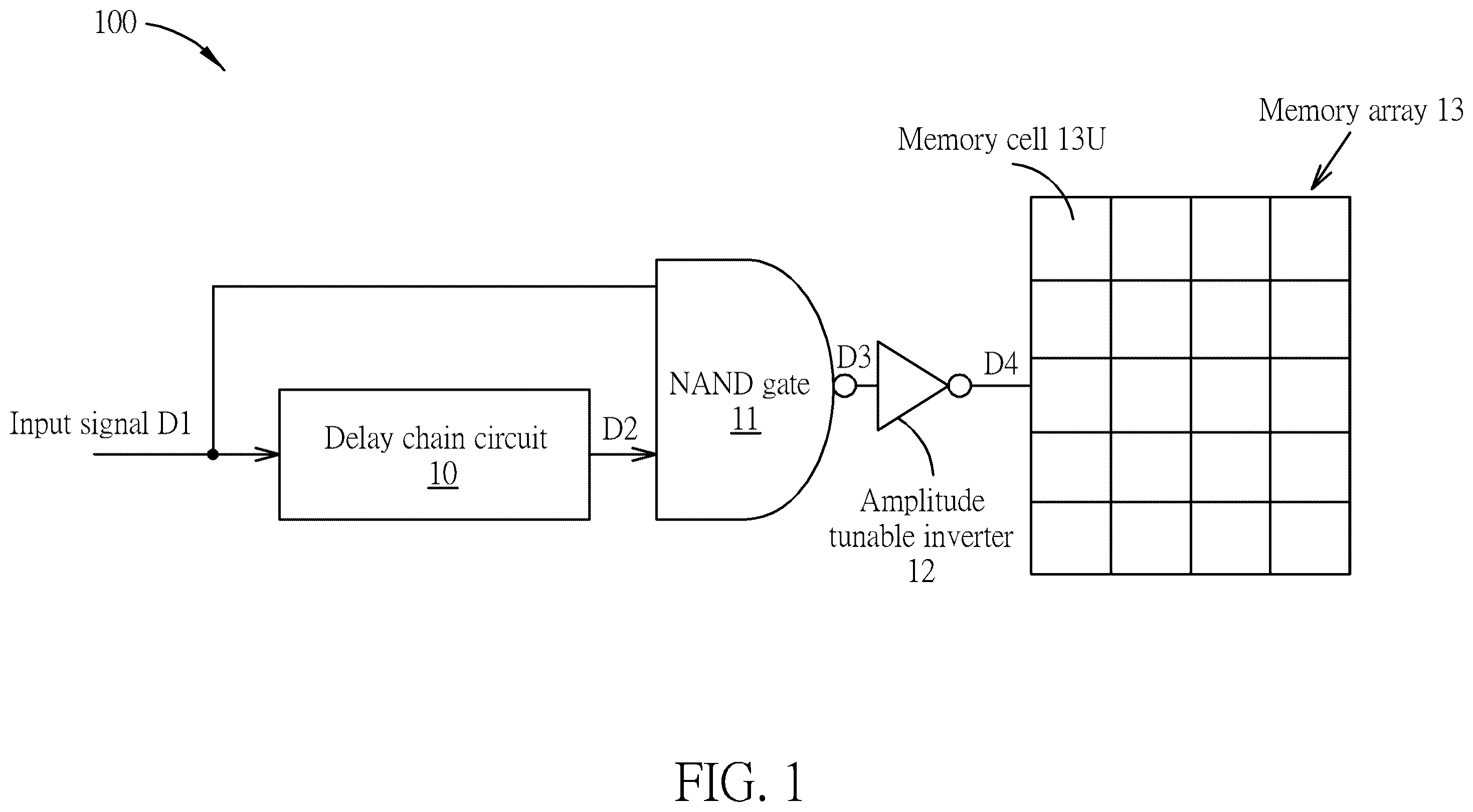
A pulse signal generator system for a magnetoresistive random access memory includes a delay chain circuit, a NAND gate, an amplitude tunable inverter, and a memory array. The delay chain circuit is used to receive an input signal and generate a delayed output signal. The NAND gate is coupled to the delay chain circuit. The NAND gate includes a first input terminal for receiving the input signal, a second input terminal for receiving the delayed output signal, and an output terminal for outputting a first pulse signal. The amplitude tunable inverter is coupled to the NAND gate. The amplitude tunable inverter includes an input terminal for receiving the first pulse signal, and an output terminal for outputting a second pulse signal. The memory array is coupled to the amplitude tunable inverter.
Claims (14)
1 . A pulse signal generator system for a magnetoresistive random access memory array comprising: a delay chain circuit configured to receive an input signal and generate a delayed output signal; a NAND gate coupled to the delay chain circuit, the NAND gate comprising: a first input terminal configured to receive the input signal; a second input terminal configured to receive the delayed output signal; and an output terminal configured to output a first pulse signal; an amplitude tunable inverter coupled to the NAND gate, the amplitude tunable inverter comprising: an input terminal configured to receive the first pulse signal; and an output terminal configured to output a second pulse signal; and a memory array coupled to the amplitude tunable inverter, the memory array comprising a plurality of memory cells each being controlled according to the second pulse signal.
Show 13 dependent claims
2 . The system of claim 1 , wherein the delay chain circuit comprises: a plurality of first inverters, wherein two adjacent first inverters of the plurality of first inverters are coupled in series through a first switch; a plurality of second switches coupled to the plurality of first inverters and the second input terminal of the NAND gate, and configured to control conduction states and cut-off states between the plurality of first inverters and the second input terminal of the NAND gate; wherein the plurality of first inverters are configured to convert the input signal to the delayed output signal.
3 . The system of claim 2 , wherein a plurality of first switches and the plurality of second switches are configured to enable odd number of first inverters of the plurality of first inverters so that a phase of the input signal and a phase of the delayed output signal are complementary.
4 . The system of claim 1 , wherein the input signal comprises a rising edge and/or a falling edge.
5 . The system of claim 1 , wherein each of the plurality of memory cells comprises: a first transistor comprising: a first terminal configured to receive a bit line voltage; a second terminal; and a control terminal; a magnetic tunnel junction component comprising: a first terminal coupled to the second terminal of the first transistor; and a second terminal; a second transistor comprising: a first terminal coupled to the second terminal of the magnetic tunnel junction component; a second terminal coupled to a ground terminal; and a control terminal coupled to the output terminal of the amplitude tunable inverter and configured to receive the second pulse signal; and at least one second inverter coupled in series between the control terminal of the second transistor and the control terminal of the first transistor.
6 . The system of claim 5 , wherein the first transistor is a P-type metal oxide semiconductor field effect transistor, the second transistor is an N-type metal oxide semiconductor field effect transistor, and when the first transistor and the second transistor are turned on, a bit line current is transmitted from the first transistor to the second transistor through the magnetic tunnel junction component.
7 . The system of claim 1 , wherein each of the plurality of memory cells comprises: a first transistor comprising: a first terminal coupled to a ground terminal; a second terminal; and a control terminal; a magnetic tunnel junction component comprising: a first terminal coupled to the second terminal of the first transistor; and a second terminal; a second transistor comprising: a first terminal coupled to the second terminal of the magnetic tunnel junction component; a second terminal configured to receive a bit line voltage; and a control terminal coupled to the output terminal of the amplitude tunable inverter and configured to receive the second pulse signal; and at least one second inverter coupled in series between the control terminal of the second transistor and the control terminal of the first transistor.
8 . The system of claim 7 , wherein the first transistor is a P-type metal oxide semiconductor field effect transistor, the second transistor is an N-type metal oxide semiconductor field effect transistor, and when the first transistor and the second transistor are turned on, a bit line current is transmitted from the second transistor to the first transistor through the magnetic tunnel junction component.
9 . The system of claim 1 , wherein when the input signal is at a high voltage and the delayed output signal is at a high voltage, the first pulse signal is at a low voltage and the second pulse signal is at a high voltage.
10 . The system of claim 1 , wherein when the input signal is at a high voltage and the delayed output signal is at a low voltage, the first pulse signal is at a high voltage and the second pulse signal is at a low voltage.
11 . The system of claim 1 , wherein when the input signal is at a low voltage and the delayed output signal is at a high voltage, the first pulse signal is at a high voltage and the second pulse signal is at a low voltage.
12 . The system of claim 1 , wherein when the input signal is at a low voltage and the delayed output signal is at a low voltage, the first pulse signal is at a high voltage and the second pulse signal is at a low voltage.
13 . The system of claim 1 , wherein the amplitude tunable inverter is an inverting amplifier, and the amplitude tunable inverter is configured to adjust an amplitude of the second pulse signal.
14 . The system of claim 1 , wherein a voltage of the second pulse signal is between 1.2 volts and 1.8 volts, and an amplitude of the input signal is smaller than an amplitude of the second pulse signal.
Full Description
Show full text →
BACKGROUND OF THE INVENTION
1. Field of the Invention The present invention relates to a pulse signal generator system for a magnetoresistive random access memory array, and more particularly, a pulse signal generator system capable of generating a pulse signal having user-defined pulse width and user-defined pulse amplitude. 2. Description of the Prior Art Magnetoresistive random access memory (MRAM) is a new type of non-volatile memory (NVM) composed of a large number of magnetic tunnel junctions (MTJs). An MTJ is a three-layer structure composed of two ferromagnetic layers sandwiching an insulating layer. The resistance of the MTJ changes depending on the relative orientation of the magnetization of the two ferromagnetic layers. The MRAM has several advantages, including non-volatility, high operational speed, high endurance, and low power consumption, which make it a promising candidate for applications in a flash memory, a dynamic random-access memory, and a static random-access memory. Further, read/write operations of the MTJ can be performed according to its resistance. Conventional method of testing the MRAM requires an MTJ data source. The MTJ data source requires to generate very short pulse signals (i.e., pulse width<500 μs) to the memory array. This may lead to high cost and throughput bottlenecks for the MTJ data source. Alternatively, additional tools, interfaces, and hardware components may be required to assisting testing operations of the MTJ data source. Therefore, developing a pulse signal generation system having high operational flexibility and low complexity for testing various MRAMs is an important design issue.
SUMMARY OF THE INVENTION
In an embodiment of the present invention, a pulse signal generator system for a magnetoresistive random access memory array is disclosed. The pulse signal generator system comprises a delay chain circuit, a NAND gate, an amplitude tunable inverter, and a memory array. The delay chain circuit is configured to receive an input signal and generate a delayed output signal. The NAND gate is coupled to the delay chain circuit. The NAND gate comprises a first input terminal configured to receive the input signal, a second input terminal configured to receive the delayed output signal, and an output terminal configured to output a first pulse signal. The amplitude tunable inverter is coupled to the NAND gate. The amplitude tunable inverter comprises an input terminal configured to receive the first pulse signal, and an output terminal configured to output a second pulse signal. The memory array is coupled to the amplitude tunable inverter. The memory array comprises a plurality of memory cells each being controlled according to the second pulse signal. These and other objectives of the present invention will no doubt become obvious to those of ordinary skill in the art after reading the following detailed description of the preferred embodiment that is illustrated in the various figures and drawings.
BRIEF DESCRIPTION OF THE DRAWINGS
is a block diagram of a pulse signal generator system for a magnetoresistive random access memory array according to an embodiment of the present invention. is an illustration of a delay chain circuit of the pulse signal generator system in . is a first circuit structure of a memory cell of the pulse signal generator system in . is a second circuit structure of the memory cell of the pulse signal generator system in . is an illustration of waveforms of an input signal, a delayed output signal, a first pulse signal, and a second pulse signal under a first state of the pulse signal generator system in . is an illustration of waveforms of the input signal, the delayed output signal, the first pulse signal, and the second pulse signal under a second state of the pulse signal generator system in . is an illustration of waveforms of the input signal, the delayed output signal, the first pulse signal, and the second pulse signal under a third state of the pulse signal generator system in . is an illustration of waveforms of the input signal, the delayed output signal, the first pulse signal, and the second pulse signal under a fourth state of the pulse signal generator system in . is an illustration of waveforms of the input signal and second pulse signals having various amplitudes of the pulse signal generator system in .
DETAILED DESCRIPTION
is a block diagram of a pulse signal generator system 100 for a magnetoresistive random access memory (MRAM) array according to an embodiment of the present invention. For presentation simplicity, it is called as the pulse signal generator system 100 hereafter. The pulse signal generator system 100 can be used for generating pulse signals having various user-defined pulse widths and amplitudes. Therefore, it can be applied to different applications of testing read/write channels of various MRAM arrays. As shown in , the pulse signal generator system 100 includes a delay chain circuit 10 , a NAND gate 11 , an amplitude tunable inverter 12 , and a memory array 13 . The delay chain circuit 10 is used for receiving an input signal D 1 to generate a delayed output signal D 2 . The NAND gate 11 is coupled to the delay chain circuit 10 . The NAND gate 11 includes a first input terminal for receiving the input signal D 1 , a second input terminal for receiving the delayed output signal D 2 , and an output terminal for outputting a first pulse signal D 3 . The amplitude tunable inverter 12 is coupled to the NAND gate 11 . The amplitude tunable inverter 12 includes an input terminal for receiving the first pulse signal D 1 , and an output terminal for outputting a second pulse signal D 4 . The memory array 13 is coupled to the amplitude tunable inverter 12 . The memory array 13 includes a plurality of memory cells 13 U. Each memory cell 13 U is controlled according to the second pulse signal D 4 . It should be understood that the memory array 13 can be an MRAM array. The structure of the MRAM array is composed of many magnetic tunnel junctions (MTJs). Further, the second pulse signal D 4 can be used for controlling at least one memory cell 13 U in the memory array 13 through a multiplexer or a selector. Any reasonable technology or hardware modification of the pulse signal generator system 100 falls into the scope of the present invention. is an illustration of the delay chain circuit 10 of the pulse signal generator system 100 . The delay chain circuit 10 includes a plurality of first inverters INVA 1 to INVAN, a plurality of first switches SW 1 ( 1 ) to SW 1 (N−1), and a plurality of second switches SW 2 ( 1 ) to SW 2 (N−1). For the plurality of first inverters INVA 1 to INVAN, two adjacent first inverters are coupled in series through a first switch. For example, the first inverter INVA 1 is coupled in series with the first inverter INVA 2 through the first switch SW 1 ( 1 ). The first inverter INVA 2 is coupled in series with the first inverter INVA 3 through the first switch SW 1 ( 2 ), and so on. The plurality of second switches SW 2 ( 1 ) to SW 2 (N−1) are coupled to the first inverters INVA 1 to INVAN and the second input terminal of the NAND gate 11 for controlling conduction states and cut-off states between the plurality of first inverters INVA 1 to INVAN and the second input terminal of the NAND gate 11 . For example, the second switch SW 2 ( 1 ) is used for controlling the conduction state and cut-off state between the output terminal of the first inverter INVA 1 and the second input terminal of the NAND gate 11 . The second switch SW 2 ( 2 ) is used for controlling the conduction state and cut-off state between the output terminal of first inverter INVA 2 and the second input terminal of the NAND gate 11 , and so on. In , the delay chain circuit 10 includes N first inverters INVA 1 to INVAN, N−1 first switches SW 1 ( 1 ) to SW 1 (N−1), and N−1 second switches SW 2 ( 1 ) to SW 2 (N−1). N can be an odd number. The first inverters INVA 1 to INVAN are used for converting an input signal D 1 into a delayed output signal D 2 . However, in other embodiments, N can also be an even number. Any reasonable design of N falls into the scope of the present invention. In the pulse signal generator system 100 , the input signal D 1 can include a rising edge and/or a falling edge. For example, a waveform of the input signal D 1 can be a square wave. After the input signal D 1 is received by delay chain circuit 10 , when an odd number of first inverters are enabled by using the first switches SW 1 ( 1 ) to SW 1 (N−1) and the second switches SW 2 ( 1 ) to SW 2 (N−1), a phase of the input signal D 1 and a phase of the delayed output signal D 2 are complementary. In other words, the delayed output signal D 2 can be regarded as the “delayed” and “inverted” input signal D 1 . is a first circuit structure of a memory cell 13 U of the pulse signal generator system 100 . As previously mentioned, the memory cell 13 U can be a magnetic tunnel junction (MTJ) memory cell. The memory cell 13 U can include a first transistor T 1 , an MTJ component 20 , a second transistor T 2 , and at least one second inverter INVB 1 to INVBM. The first transistor T 1 includes a first terminal for receiving a bit line voltage Vwr, a second terminal, and a control terminal. The MTJ component 20 includes a first terminal coupled to the second terminal of the first transistor T 1 , and a second terminal. The second transistor T 2 includes a first terminal coupled to the second terminal of the MTJ component 20 , a second terminal coupled to the ground terminal, and a control terminal coupled to the output terminal of the amplitude tunable inverter 12 for receiving the second pulse signal D 4 . At least one second inverter INVB 1 to INVBM is coupled in series between the control terminal of the second transistor T 2 and the control terminal of the first transistor T 1 . Mis a positive integer. Further, the first transistor T 1 can be a P-type metal-oxide-semiconductor field-effect transistor (P-MOS). The second transistor T 2 can be an N-type metal-oxide-semiconductor field-effect transistor (N-MOS). It should be understood that the MTJ component 20 is a three-layer structure composed of two ferromagnetic layers sandwiching an insulating layer. Its resistance changes with the relative direction of magnetization of the two ferromagnetic layers. Particularly, the read/write operations of the MTJ can be performed according to its resistance. In , when the first transistor T 1 and the second transistor T 2 are turned on, a bit line current IB 1 is transmitted from the first transistor T 1 to the second transistor T 2 through the MTJ component 20 . In other words, the pulse width (i.e., a high voltage duration) of the second pulse signal D 4 determines a time length of turning on the first transistor T 1 and the second transistor T 2 . The pulse amplitude of the second pulse signal D 4 determines a magnitude of the bit line current IB 1 transmitted from the first transistor T 1 to the second transistor T 2 . Adjustments of the pulse width and the pulse amplitude of the second pulse signal D 4 are illustrated later. is a second circuit structure of the memory cell 13 U of the pulse signal generator system 100 . In , the memory cell 13 U can include the first transistor T 1 , the MTJ component 20 , the second transistor T 2 , and the at least one second inverter INVB 1 to INVBM. Specifically, since the circuit structure of the memory cell 13 U in is similar to the circuit structure of the memory cell 13 U in , all component symbols are reused. A difference between and lies in that the first terminal of the first transistor T 1 is coupled to the ground terminal. The second terminal of the second transistor T 2 is used for receiving the bit line voltage Vwr. Therefore, in , when the first transistor T 1 and the second transistor T 2 are turned on, the bit line current IB 2 is transmitted from the second transistor T 2 to the first transistor T 1 through the MTJ component 20 . Similarly, the pulse width (i.e., a high voltage duration) of the second pulse signal D 4 determines a time length of turning on the first transistor T 1 and the second transistor T 2 . The pulse amplitude of the second pulse signal D 4 determines a magnitude of the bit line current IB 2 transmitted from the second transistor T 2 to the first transistor T 1 . In the pulse signal generator system 100 , as previously mentioned, the delayed output signal D 2 can be regarded as the “delayed” and “inverted” input signal D 1 . The input signal D 1 and the delayed output signal D 2 are inputted to the NAND gate 11 . Moreover, a truth table of the NAND gate 11 can be listed in Table T 1 . TABLE T1 input delayed output first pulse signal D1 signal D2 signal D3 Low voltage Low voltage High voltage Low voltage High voltage High voltage High voltage Low voltage High voltage High voltage High voltage Low voltage As shown in Table T 1 , when both the input signal D 1 and the delayed output signal D 2 are at a high voltage for a certain time period, the first pulse signal D 3 is at a low voltage for the time period. Moreover, the amplitude tunable inverter 11 can be an inverting amplifier. After the first pulse signal D 3 is received by the amplitude tunable inverter 11 , the amplitude tunable inverter 11 adjusts its amplitude, inverts its phase, and then generates the output as the second pulse signal D 4 . Therefore, by using the amplitude tunable inverter 11 , when both the input signal D 1 and the delayed output signal D 2 are at the high voltage for a certain time period, the second pulse signal D 4 is at a high voltage for the time period. It should be understood that an overlap time length of high voltage states of the input signal D 1 and the delayed output signal D 2 can be adjusted according to a delay time of the delayed output signal D 2 . The delay time of the delayed output signal D 2 can be adjusted according to the number of inverters turned on in the delay chain circuit 10 . Therefore, in the pulse signal generator system 100 , by adjusting the number of inverters in the delay chain circuit 10 that are turned on by the first switches and the second switches, the pulse width of the second pulse signal D 4 can be user-defined. Moreover, the pulse amplitude of the second pulse signal D 4 can also be adjusted by using the amplitude tunable inverter 11 . Therefore, the pulse signal generator system 100 can generate pulse signals having user-defined pulse widths and amplitudes in a low-complexity manner. is an illustration of waveforms of the input signal D 1 , the delayed output signal D 2 , the first pulse signal D 3 , and the second pulse signal D 4 under a first state of the pulse signal generator system. X-axis is denoted as a time line. Y-axis is denoted as a voltage line. The input signal D 1 is a square wave having a fixed width (i.e., 500 μs) and amplitude Vcc. The delayed output signal D 2 can be regarded as an inverted waveform of the input signal D 1 delayed by a time period Tdelay (say, a delay time Tdelay, hereafter). In the first time period P 1 , the input signal D 1 is at a low voltage. The delayed output signal D 2 is at a high voltage. According to the truth table of the NAND gate 11 (as shown in Table 1), the first pulse signal D 3 is at a high voltage. The second pulse signal D 4 is at a low voltage. Therefore, when phases of the input signal D 1 and the delayed output signal D 2 are different (i.e. low voltage and high voltage) during the first time period P 1 , the voltage of the second pulse signal D 4 cannot be boosted during the first time period P 1 . is an illustration of waveforms of the input signal D 1 , the delayed output signal D 2 , the first pulse signal D 3 , and the second pulse signal D 4 under a second state of the pulse signal generator system. X-axis is denoted as the time line. Y-axis is denoted as the voltage line. The input signal D 1 is the square wave having the fixed width (i.e., 500 μs) and the amplitude Vcc. The delayed output signal D 2 can be regarded as the inverted waveform of the input signal D 1 delayed by the delay time Tdelay. In the second time period P 2 , the input signal D 1 is at a high voltage. The delayed output signal D 2 is at a high voltage. According to the truth table of the NAND gate 11 (as shown in Table 1), the first pulse signal D 3 is at a low voltage. The second pulse signal D 4 is at a high voltage. Its pulse amplitude can be adjusted as Vcc′. Therefore, when both the input signal D 1 and the delayed output signal D 2 are at the high voltages during the second time period P 2 , the voltage of the second pulse signal D 4 can be boosted during the second time period P 1 . is an illustration of waveforms of the input signal D 1 , the delayed output signal D 2 , the first pulse signal D 3 , and the second pulse signal D 4 under a third state of the pulse signal generator system 100 . X-axis is denoted as the time line. Y-axis is denoted as the voltage line. The input signal D 1 is the square wave having the fixed width (i.e., 500 μs) and the amplitude Vcc. The delayed output signal D 2 can be regarded as the inverted waveform of the input signal D 1 delayed by the delay time Tdelay. In the third time period P 3 , the input signal D 1 is at a high voltage. The delayed output signal D 2 is at a low voltage. According to the truth table of the NAND gate 11 (as shown in Table 1), the first pulse signal D 3 is at a high voltage. The second pulse signal D 4 is at a low voltage. Therefore, when phases of the input signal D 1 and the delayed output signal D 2 are different (i.e. high voltage and low voltage) during the third time period P 3 , the voltage of the second pulse signal D 4 cannot be boosted during the third time period P 3 . is an illustration of waveforms of the input signal D 1 , the delayed output signal D 2 , the first pulse signal D 3 , and the second pulse signal D 4 under a fourth state of the pulse signal generator system 100 . X-axis is denoted as the time line. Y-axis is denoted as the voltage line. The input signal D 1 is the square wave having the fixed width (i.e., 500 μs) and the amplitude Vcc. The delayed output signal D 2 can be regarded as the inverted waveform of the input signal D 1 delayed by the delay time Tdelay. In the fourth time period P 4 , the input signal D 1 is at a low voltage. The delayed output signal D 2 is at a low voltage. According to the truth table of the NAND gate 11 (as shown in Table 1), the first pulse signal D 3 is at a high voltage. The second pulse signal D 4 is at a low voltage. Therefore, when both the input signal D 1 and the delayed output signal D 2 are at the low voltages during the fourth time period P 4 , the voltage of the second pulse signal D 4 cannot be boosted during the fourth time period P 4 . As shown in to , the delay time Tdelay is introduced between the input signal D 1 and the delayed output signal D 2 . During the delay time Tdelay, both the input signal D 1 and the output signal D 2 are at high voltages. Therefore, a time period of the second pulse signal D 4 being at a high voltage (say, “pulse width” of the second pulse signal D 4 ) is equal to the delay time Tdelay. Therefore, in the pulse signal generator system 100 , by adjusting the delay time Tdelay, the second pulse signal D 4 having a pulse width equal to Tdelay can be generated. is an illustration of waveforms of the input signal D 1 and second pulse signals D 4 having various amplitudes of the pulse signal generator system 100 . X-axis is denoted as the time line. Y-axis is denoted as the voltage line. As previously mentioned, in the pulse signal generator system 100 , the pulse amplitude of the second pulse signal D 4 can be adjusted by using the amplitude tunable inverter 12 . For example, the pulse amplitude Amp 1 of the input signal D 1 is one volt (1V). After adjusting the pulse amplitude by using the amplitude tunable inverter 12 , the pulse amplitude Amp 2 of the second pulse signal D 4 can be 1.2 volts (1.2V). In other embodiments, the pulse amplitude Amp 3 of the second pulse signal D 4 can be 1.4 volts (1.4V). The pulse amplitude Amp 4 of the second pulse signal D 4 can also be 1.8 volts (1.8V). In other words, in the embodiment of , the pulse amplitude of the second pulse signal D 4 is between 1.2 volts and 1.8 volts. Further, an amplitude of the input signal D 1 is smaller than an amplitude of the second pulse signal D 4 . However, the present invention is not limited thereto. In other embodiments, the pulse amplitude of the second pulse signal D 4 can be adjusted to any voltage supported by the amplitude tunable inverter 12 . To sum up, the present invention discloses a pulse signal generator system for a magnetoresistive random access memory array. The pulse signal generator system introduces the delay chain circuit for delaying the input signal. Further, the pulse signal generator system introduces the NAND gate and the amplitude tunable inverter. After receiving the input signal and the delayed output signal by the NAND gate, the amplitude tunable inverter can output the pulse signal having user-defined pulse width and user-defined pulse amplitude. Moreover, in the pulse signal generator system, the pulse width of the output pulse signal can be determined according to the number of inverters in the delay chain circuit turned on by the first switches and the second switches. Furthermore, the pulse amplitude of the output pulse signal can also be adjusted according to a voltage gain of the amplitude tunable inverter. Therefore, the pulse signal generator system can generate pulse signals having user-defined pulse widths and amplitudes in the low-complexity manner. Those skilled in the art will readily observe that numerous modifications and alterations of the device and method may be made while retaining the teachings of the invention. Accordingly, the above disclosure should be construed as limited only by the metes and bounds of the appended claims.
Figures (9)
Citations
This patent cites (9)
- US9741455
- US11335387
- US2003/0179612
- US2008/0151656
- US2016/0352350
- US2018/0039532
- US2025/0374554
- USI427906
- US2017176217