Display Device and Mobile Electronic Device Including the Same
Abstract
A display device and a mobile electronic device including the display device each include a substrate, a driving element layer on the substrate and including pixel driving circuits for driving pixels, and a light emitting element layer on the driving element layer and including a light emitting element of each pixel. Transistors included in each pixel driving circuit are divided into a first transistor group and a second transistor group connected to a first well region and a second well region of the substrate, respectively, the first and second well regions in each pixel are spaced apart from each other by a first interval, the pixels include a first pixel and a second pixel adjacent to each other in a first direction, and well regions adjacent to each other in the first pixel and the second pixel are spaced apart from each other by the first interval.
Claims (20)
1 . A display device comprising: a substrate; a driving element layer disposed on the substrate and including a plurality of pixel driving circuits for driving a plurality of pixels; and a light emitting element layer disposed on the driving element layer and including a light emitting element of each of the plurality of pixels, wherein transistors included in each of the plurality of pixel driving circuits are divided into a first transistor group connected to a first well region of the substrate and a second transistor group connected to a second well region of the substrate, the first well region and the second well region in each of the plurality of pixels are defined in a same surface portion of the substrate, the first well region and the second well region in each of the plurality of pixels are spaced apart from each other by a first interval when viewed in a thickness direction of the substrate, the plurality of pixels includes a first pixel and a second pixel adjacent to each other in a first direction, and well regions adjacent to each other in the first pixel and the second pixel are spaced apart from each other by the first interval when viewed in the thickness direction of the substrate, wherein the first pixel is adjacent to the second pixel in the first direction, and wherein the first well region included in the first pixel is spaced apart from the first well region or the second well region of the second pixel by a second interval which is greater than the first interval.
11 . A mobile electronic device comprising: a display device including a display panel in which a light emitting element is disposed on a substrate, wherein the display panel includes: a driving element layer disposed on the substrate and including a plurality of pixel driving circuits for driving a plurality of pixels; and a light emitting element layer disposed on the driving element layer and including the light emitting element of each of the plurality of pixels, wherein transistors included in each of the plurality of pixel driving circuits are divided into a first transistor group connected to a first well region of the substrate and a second transistor group connected to a second well region of the substrate, the first well region and the second well region in each of the plurality of pixels are defined in a same surface portion of the substrate, the first well region and the second well region in each of the plurality of pixels are spaced apart from each other by a first interval when viewed in a thickness direction of the substrate, the plurality of pixels include a first pixel and a second pixel adjacent to each other in a first direction, and well regions adjacent to each other in the first pixel and the second pixel are spaced apart from each other by the first interval when viewed in the thickness direction of the substrate, wherein the first pixel is adjacent to the second pixel in the first direction, and wherein the first well region included in the first pixel is spaced apart from the first well region or the second well region of the second pixel by a second interval which is greater than the first interval.
Show 18 dependent claims
2 . The display device of claim 1 , wherein a first body voltage is input to the first well region as a body bias voltage of the first transistor group, and a second body voltage is input to the second well region as a body bias voltage of the second transistor group.
3 . The display device of claim 2 , wherein the first well region and the second well region in each of the plurality of pixels are spaced apart from each other by the first interval in the first direction.
4 . The display device of claim 3 , wherein the first well region included in the first pixel is spaced apart from the first well region or the second well region included in the second pixel by the first interval in the first direction.
5 . The display device of claim 4 , wherein the plurality of pixels further includes a third pixel adjacent to the first pixel in a second direction perpendicular to the first direction, and the first well region included in the first pixel is spaced apart from the first well region or the second well region included in the third pixel by the second interval.
6 . The display device of claim 4 , wherein the plurality of pixels further includes a third pixel adjacent to the first pixel in a second direction perpendicular to the first direction, and the first well region included in the first pixel is spaced apart from the first well region or the second well region included in the third pixel by the first interval in the second direction.
7 . The display device of claim 6 , wherein the first direction is a short side direction of the display device, and the second direction is a long side direction of the display device.
8 . The display device of claim 6 , wherein the first direction is a long side direction of the display device, and the second direction is a short side direction of the display device.
9 . The display device of claim 1 , wherein the first transistor group includes a driving transistor which supplies a driving current to the light emitting element, and the second transistor group includes at least one switching transistor which controls a voltage of a node included in the pixel driving circuit.
10 . The display device of claim 1 , wherein the transistors included in each of the plurality of pixel driving circuits are P-type metal oxide semiconductor field effect transistors or N-type metal oxide semiconductor field effect transistors.
12 . The mobile electronic device of claim 11 , wherein a first body voltage is input to the first well region as a body bias voltage of the first transistor group, and a second body voltage is input to the second well region as a body bias voltage of the second transistor group.
13 . The mobile electronic device of claim 12 , wherein the first well region and the second well region in each of the plurality of pixels are spaced apart from each other by the first interval in the first direction.
14 . The mobile electronic device of claim 13 , wherein the first well region included in the first pixel is spaced apart from the first well region or the second well region included in the second pixel by the first interval in the first direction.
15 . The mobile electronic device of claim 14 , wherein the plurality of pixels further includes a third pixel adjacent to the first pixel in a second direction perpendicular to the first direction, and the first well region included in the first pixel is spaced apart from the first well region or the second well region included in the third pixel by the second interval.
16 . The mobile electronic device of claim 14 , wherein the plurality of pixels further includes a third pixel adjacent to the first pixel in a second direction perpendicular to the first direction, and the first well region included in the first pixel is spaced apart from the first well region or the second well region included in the third pixel by the first interval in the second direction.
17 . The mobile electronic device of claim 16 , wherein the first direction is a short side direction of the display device, and the second direction is a long side direction of the display device.
18 . The mobile electronic device of claim 16 , wherein the first direction is a long side direction of the display device, and the second direction is a short side direction of the display device.
19 . The mobile electronic device of claim 11 , wherein the first transistor group includes a driving transistor which supplies a driving current to the light emitting element, and the second transistor group includes at least one switching transistor which controls a voltage of a node included in the pixel driving circuit.
20 . The mobile electronic device of claim 11 , wherein the transistors included in each of the plurality of pixel driving circuits are P-type metal oxide semiconductor field effect transistors or N-type metal oxide semiconductor field effect transistors.
Full Description
Show full text →
This application claims priority to Korean Patent Application No. 10-2023-0093185, filed on Jul. 18, 2023, and all the benefits accruing therefrom under 35 U.S.C. 119, the content of which in its entirety is herein incorporated by reference.
BACKGROUND
1. Field The disclosure relates to a display device and a mobile electronic device including the display device. 2. Description of the Related Art A wearable device that is developed in the form of glasses or a helmet and focuses on a distance close to the user's eyes is being developed. For example, the wearable device may be a head mounted display (HMD) device or augmented reality (AR) glass. Such a wearable device provides a user with an AR screen or a virtual reality (VR) screen. The wearable device such as the HMD device or the AR glass may be desired to have a display specification of at least 2000 pixels per inch (PPI) to allow the user to use the device for a long time without feeling dizzy. Accordingly, organic light emitting diode on silicon (OLEDoS) technology, which is a small organic light emitting display device with high resolution, may be used to realize the wearable device. The OLEDoS is a technology that disposes organic light emitting diodes (OLEDs) on a semiconductor wafer substrate on which a complementary metal oxide semiconductor (CMOS) is disposed.
SUMMARY
Embodiments of the disclosure provide a display device capable of increasing the degree of integration of pixels and providing an ultra-high resolution display panel by reducing a separation distance between transistors forming a pixel driving circuit, and a mobile electronic device including the same. According to an embodiment of the disclosure, a display device includes a substrate, a driving element layer disposed on the substrate and including a plurality of pixel driving circuits for driving a plurality of pixels, and a light emitting element layer disposed on the driving element layer and including a light emitting element of each of the plurality of pixel. In such an embodiment, transistors included in each of the plurality of pixel driving circuits are divided into a first transistor group connected to a first well region of the substrate and a second transistor group connected to a second well region of the substrate, the first well region and the second well region are disposed to be spaced apart from each other by a first interval, the plurality of pixels include a first pixel and a second pixel disposed to be adjacent to each other in a first direction, and well regions adjacent to each other in the first pixel and the second pixel are disposed to be spaced apart from each other by the first interval. In an embodiment, a first body voltage may be input to the first well region as a body bias voltage of the first transistor group, and a second body voltage may be input to the second well region as a body bias voltage of the second transistor group. In an embodiment, the first well region and the second well region in each of the plurality of pixels may be disposed to be spaced apart from each other by the first interval in a first direction. In an embodiment, a first well region included in the first pixel may be disposed to be spaced apart from a first well region or a second well region included in the second pixel by the first interval in the first direction. In an embodiment, the plurality of pixels may further include a third pixel disposed to be adjacent to the first pixel in a second direction perpendicular to the first direction, and the first well region included in the first pixel may be disposed to be spaced apart from a first well region or a second well region included in the third pixel by a second interval greater than the first interval in the second direction. In an embodiment, the plurality of pixels may further include a third pixel disposed to be adjacent to the first pixel in a second direction perpendicular to the first direction, and the first well region included in the first pixel may be disposed to be spaced apart from a first well region or a second well region included in the third pixel by the first interval in the second direction. In an embodiment, the first direction may be a short side direction of the display device, and the second direction may be a long side direction of the display device. In an embodiment, the first direction may be a long side direction of the display device, and the second direction may be a short side direction of the display device. In an embodiment, the first transistor group may include a driving transistor which supplies a driving current to the light emitting element, and the second transistor group includes at least one switching transistor which controls a voltage of a node included in the pixel driving circuit. In an embodiment, the transistors included in each of the plurality of pixel driving circuits may be P-type metal oxide semiconductor field effect transistors (MOSFETs) or N-type MOSFETs. According to an embodiment of the disclosure, a mobile electronic device includes a display device including a display panel in which a light emitting element is disposed on a substrate. In such an embodiment, the display panel includes a driving element layer disposed on the substrate and including a plurality of pixel driving circuits for driving a plurality of pixels, and a light emitting element layer disposed on the driving element layer and including the light emitting element of each of the plurality of pixels, where transistors included in each of the plurality of pixel driving circuits are divided into a first transistor group connected to a first well region of the substrate and a second transistor group connected to a second well region of the substrate, the first well region and the second well region in each of the plurality of pixels are disposed to be spaced apart from each other by a first interval, the plurality of pixels include a first pixel and a second pixel disposed to be adjacent to each other in a first direction, and well regions adjacent to each other in the first pixel and the second pixel are disposed to be spaced apart from each other by the first interval. In an embodiment, a first body voltage may be input to the first well region as a body bias voltage of the first transistor group, and a second body voltage may be input to the second well region as a body bias voltage of the second transistor group. In an embodiment, the first well region and the second well region in each of the plurality of pixels may be disposed to be spaced apart from each other by the first interval in a first direction. In an embodiment, a first well region included in the first pixel may be disposed to be spaced apart from a first well region or a second well region included in the second pixel by the first interval in the first direction. In an embodiment, the plurality of pixels may further include a third pixel disposed to be adjacent to the first pixel in a second direction perpendicular to the first direction, and the first well region included in the first pixel may be disposed to be spaced apart from a first well region or a second well region included in the third pixel by a second interval greater than the first interval in the second direction. In an embodiment, the plurality of pixels may further include a third pixel disposed to be adjacent to the first pixel in a second direction perpendicular to the first direction, and the first well region included in the first pixel may be disposed to be spaced apart from a first well region or a second well region included in the third pixel by the first interval in the second direction. In an embodiment, the first direction may be a short side direction of the display device, and the second direction may be a long side direction of the display device. In an embodiment, the first direction may be a long side direction of the display device, and the second direction may be a short side direction of the display device. In an embodiment, the first transistor group may include a driving transistor which supplies a driving current to the light emitting element, and the second transistor group includes at least one switching transistor which controls a voltage of a node included in the pixel driving circuit. In an embodiment, the transistors included in each of the plurality of pixel driving circuits may be P-type MOSFETs or N-type MOSFETs. According to embodiments of the display device and the mobile electronic device including the display device, by reducing the separation distance between the transistors of the pixel driving circuit, the degree of integration of pixels may be increased and the ultra-high resolution display panel may be provided. However, embodiments of the disclosure are not restricted to those set forth herein. The above and other features of embodiments of the disclosure will become more apparent to one of ordinary skill in the art to which the present disclosure pertains by referencing the detailed description below.
BRIEF DESCRIPTION OF THE DRAWINGS
The above and other features of embodiments of the disclosure will become more apparent by describing in detail embodiments thereof with reference to the attached drawings, in which: is a perspective view illustrating a display device according to an embodiment; is a plan view illustrating a display panel according to an embodiment; is a configuration block diagram of the display device according to an embodiment; is a circuit diagram of one pixel of the display device according to an embodiment; is a view schematically illustrating a cross-section of a portion of the display panel of the display device according to an embodiment; are plan views illustrating a first well region and a second well region disposed in one pixel of the display device according to an embodiment; is a plan view schematically illustrating a portion of a display panel according to a comparative example; is a cross-sectional view schematically illustrating a cross-section of a portion of the display panel according to the comparative example taken along line A-A′ of ; is a plan view schematically illustrating a portion of the display panel according to an embodiment; is a cross-sectional view schematically illustrating a cross-section of a portion of the display panel according to an embodiment taken along line B-B′ of ; is a plan view schematically illustrating a display panel according to an embodiment in which an interval between well regions between two pixels adjacent in a first direction is adjusted; is a plan view schematically illustrating a display panel according to an embodiment in which an interval between well regions between two pixels adjacent in a second direction is adjusted; is a view illustrating a virtual reality device including the display device according to an embodiment; and are views illustrating an HMD device to which the display device according to an embodiment is applied.
DETAILED DESCRIPTION
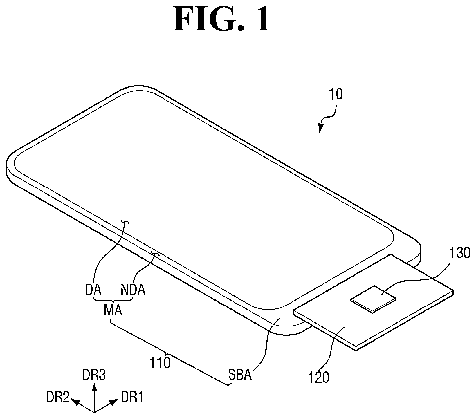
The invention now will be described more fully hereinafter with reference to the accompanying drawings, in which various embodiments are shown. This invention may, however, be embodied in many different forms, and should not be construed as limited to the embodiments set forth herein. Rather, these embodiments are provided so that this disclosure will be thorough and complete, and will fully convey the scope of the invention to those skilled in the art. Like reference numerals refer to like elements throughout. It will be understood that when an element is referred to as being “on” another element, it can be directly on the other element or intervening elements may be present therebetween. In contrast, when an element is referred to as being “directly on” another element, there are no intervening elements present. It will be understood that, although the terms “first,” “second,” etc. may be used herein to describe various elements, these elements should not be limited by these terms. These terms are only used to distinguish one element from another element. For instance, a first element discussed below could be termed a second element without departing from the teachings of the present invention. Similarly, the second element could also be termed the first element. The terminology used herein is for the purpose of describing particular embodiments only and is not intended to be limiting. As used herein, “a”, “an,” “the,” and “at least one” do not denote a limitation of quantity, and are intended to include both the singular and plural, unless the context clearly indicates otherwise. Thus, reference to “an” element in a claim followed by reference to “the” element is inclusive of one element and a plurality of the elements. For example, “an element” has the same meaning as “at least one element,” unless the context clearly indicates otherwise. “At least one” is not to be construed as limiting “a” or “an.” “Or” means “and/or.” As used herein, the term “and/or” includes any and all combinations of one or more of the associated listed items. It will be further understood that the terms “comprises” and/or “comprising,” or “includes” and/or “including” when used in this specification, specify the presence of stated features, regions, integers, steps, operations, elements, and/or components, but do not preclude the presence or addition of one or more other features, regions, integers, steps, operations, elements, components, and/or groups thereof. Furthermore, relative terms, such as “lower” or “bottom” and “upper” or “top,” may be used herein to describe one element's relationship to another element as illustrated in the Figures. It will be understood that relative terms are intended to encompass different orientations of the device in addition to the orientation depicted in the Figures. For example, if the device in one of the figures is turned over, elements described as being on the “lower” side of other elements would then be oriented on “upper” sides of the other elements. The term “lower,” can therefore, encompasses both an orientation of “lower” and “upper,” depending on the particular orientation of the figure. Similarly, if the device in one of the figures is turned over, elements described as “below” or “beneath” other elements would then be oriented “above” the other elements. The terms “below” or “beneath” can, therefore, encompass both an orientation of above and below. “About” or “approximately” as used herein is inclusive of the stated value and means within an acceptable range of deviation for the particular value as determined by one of ordinary skill in the art, considering the measurement in question and the error associated with measurement of the particular quantity (i.e., the limitations of the measurement system). For example, “about” can mean within one or more standard deviations, or within ±30%, 20%, 10% or 5% of the stated value. Unless otherwise defined, all terms (including technical and scientific terms) used herein have the same meaning as commonly understood by one of ordinary skill in the art to which this disclosure belongs. It will be further understood that terms, such as those defined in commonly used dictionaries, should be interpreted as having a meaning that is consistent with their meaning in the context of the relevant art and the disclosure, and will not be interpreted in an idealized or overly formal sense unless expressly so defined herein. Embodiments are described herein with reference to cross section illustrations that are schematic illustrations of idealized embodiments. As such, variations from the shapes of the illustrations as a result, for example, of manufacturing techniques and/or tolerances, are to be expected. Thus, embodiments described herein should not be construed as limited to the particular shapes of regions as illustrated herein but are to include deviations in shapes that result, for example, from manufacturing. For example, a region illustrated or described as flat may, typically, have rough and/or nonlinear features. Moreover, sharp angles that are illustrated may be rounded. Thus, the regions illustrated in the figures are schematic in nature and their shapes are not intended to illustrate the precise shape of a region and are not intended to limit the scope of the present claims. Hereinafter, embodiments of the disclosure will be described in detail with reference to the accompanying drawings. is a perspective view illustrating a display device according to an embodiment. Referring to , an embodiment of a display device 10 may be applied to portable electronic devices such as a mobile phone, a smartphone, a tablet personal computer (PC), a mobile communication terminal, an electronic notebook, an electronic book, a portable multimedia player (PMP), navigation, and an ultra mobile PC (UMPC). In an embodiment, for example, the display device 10 may be applied to a display unit of a television, a laptop computer, a monitor, a billboard, or the Internet of Things (IOT) device. In an embodiment, for example, the display device 10 may be applied to a wearable device such as a smart watch, a watch phone, a glasses-type display, and a head mounted display (HMD). The display device 10 may be formed in a planar shape similar to a quadrangle. In an embodiment, for example, the display device 10 may have a planar shape similar to a quadrangle having a short side in a first direction DR 1 and a long side in a second direction DR 2 . Alternatively, the display device 10 may have a planar shape similar to a quadrangle having a long side in a first direction DR 1 and a short side in a second direction DR 2 crossing the first direction DR 1 . In , a third direction DR 3 indicates a normal direction perpendicular to a plane defined by the first direction DR 1 and the second direction DR 2 . The third direction DR 3 may be a thickness direction of the display device 10 . A corner where the short side and the long side meet may be formed to be rounded to have a predetermined curvature or formed at a right angle. In embodiments, the planar shape of the display device 10 is not limited to the quadrangle, and may be formed similarly to other polygons, circles, or ovals. In an embodiment, the display device 10 includes a display panel 110 , a circuit board 120 , and a power supply unit 130 . The display panel 110 is a display panel 110 including a semiconductor wafer substrate ( 200 in ) as a base substrate. The display panel 110 may include a main area MA and a sub-area SBA. The main area MA may include a display area DA including pixels (PX in ) for displaying an image, and a non-display area NDA disposed around the display area DA. The non-display area NDA may refer to an area other than the display area DA. The display area DA may emit light from a plurality of light emitting areas or a plurality of opening areas. In an embodiment, for example, the display panel 110 may include a pixel driving circuit (PC in ) including switching elements, a pixel defining film defining a light emitting area or an opening area, and a light emitting element (LEL in ) that is a self-light emitting element. The light emitting element LEL may include at least one selected from an organic light emitting diode (LED) including an organic light emitting layer, a quantum dot LED including a quantum dot light emitting layer, an inorganic LED including an inorganic semiconductor, and a micro LED, but is not limited thereto. The non-display area NDA may be an area outside the display area DA. The non-display area NDA may be defined as an edge area of the main area MA of the display panel 110 . The non-display area NDA may include fan-out lines (not illustrated) extending from lines (e.g., a gate line, a data line, and an emission control line) of the display area DA and a display pad portion (not illustrated). The sub-area SBA may extend from one side of the main area MA. The sub-area SBA may include a main pad portion connected to the circuit board 120 . Optionally, the sub-area SBA may be omitted, and the main pad portion may be disposed in the non-display area NDA. The circuit board 120 may be attached onto the main pad portion of the display panel 110 using an anisotropic conductive film (ACF). Lead lines of the circuit board 120 may be electrically connected to the main pad portion of the display panel 110 . The circuit board 120 may be a flexible printed circuit board, a printed circuit board, or a flexible film such as a chip on film. The power supply unit 130 may be disposed on the circuit board 120 , and may supply a power voltage to the display driving circuit ( 210 in ) and the display panel 110 . The power supply unit 130 may generate a driving voltage and supply the driving voltage to a driving voltage line. In an embodiment, for example, the driving voltage may include a high-potential voltage (a first driving voltage, ELVDD in ), a low-potential voltage (a second driving voltage, ELVSS in ), and an initialization voltage (VINT in ) for driving the light emitting element LEL. is a plan view illustrating a display panel according to an embodiment. Referring to , an embodiment of the display panel 110 may be an organic light emitting diode on silicon (OLEDoS) panel including the semiconductor wafer substrate 200 as a base substrate. In an embodiment, for example, the display panel 110 may include the semiconductor wafer substrate 200 , and the pixel driving circuit (PC in ) and the display driving circuit 210 for controlling the pixel driving circuit PC may be disposed on a front surface 201 of the semiconductor wafer substrate 200 . The pixel driving circuit PC is disposed to overlap the light emitting element (LEL in ) of each pixel (PX in ) in the display area DA. The display driving circuit 210 is disposed in the non-display area NDA and serves to drive the pixel driving circuits PC. Herein, the semiconductor wafer substrate 200 may be referred to as a “substrate” or a “circuit board”. The pixel driving circuit (PC in ) and the display driving circuit 210 may be formed on a metal oxide semiconductor field effect transistor (MOSFET) layer 501 disposed on the front surface 201 of the semiconductor wafer substrate 200 . The MOSFET layer 501 may include, for example, an N-type MOSFET and/or a P-type MOSFET. Herein, the MOSFET layer ( 501 in ) may be referred to as a “drive element layer”. is a configuration block diagram of the display device according to an embodiment. Referring to , an embodiment of the display device 10 includes a display panel 110 based on the semiconductor wafer substrate 200 . The display driving circuit 210 may be embedded in the display panel 110 . In an embodiment, the display driving circuit 210 may be formed on the MOSFET layer 501 disposed on the front surface 201 of the semiconductor wafer substrate 200 . The display driving circuit 210 may include a timing controller 310 , a gate driver 320 , an emission control driver 330 , and a data driver 340 , but the disclosure is not limited thereto. Although not illustrated, the display driving circuit 210 may further include a memory (e.g., a one-time-programmable memory (OTP)), an interface circuit (I/F), an image processing circuit (e.g., logic circuitry), and/or a gamma processing circuit. The display area DA of the display panel 110 includes a plurality of pixels PX disposed in a matrix form. Each of the plurality of pixels PX may be connected to a first driving voltage line VDL, a second driving voltage line VSL, a gate line GL, an emission control line EML, an initialization line VIL, and a data line DL. The first driving voltage line VDL supplies the first driving voltage (ELVDD in ) input from the power supply unit 130 to the plurality of pixels PX. The second driving voltage line VSL supplies the second driving voltage (ELVSS in ) input from the power supply unit 130 to the plurality of pixels PX. The gate line GL supplies gate signals (GI and GW in ) input from the gate driver 320 to the plurality of pixels PX. The emission control line EML supplies the emission control signal (EM in ) input from the emission control driver 330 to the plurality of pixels PX. The initialization line VIL supplies the initialization voltage (VINT in ) input from the power supply unit 130 to the plurality of pixels PX. The data line DL supplies analog data voltages input from the data driver 340 to the pixels PX. The first driving voltage ELVDD may be a high-potential voltage, and the second driving voltage ELVSS may be a low-potential voltage. In an embodiment, for example, the first driving voltage ELVDD may have a potential higher than that of the second driving voltage ELVSS. The initialization voltage (VINT in ) may have a potential for initializing the pixel driving circuit (PC in ) for each frame. One gate line GL illustrated in may include a first gate line GWL and a second gate line GIL, but the disclosure is not limited thereto. Each of the plurality of pixels PX includes the light emitting element (LEL in ), and may include a plurality of transistors and one or more capacitors as the pixel driving circuit (PC in ) for driving the light emitting element LEL. The timing controller 310 may receive a data signal DATA and timing signals from the circuit board 120 . The timing controller 310 may control an operation timing of the data driver 340 by generating a data control signal DCS based on the timing signals. The timing controller 310 may control an operation timing of the gate driver 320 by generating a gate control signal GCS based on the timing signals. The timing controller 310 may control an operation timing of the emission control driver 330 by generating an emission control signal ECS based on the timing signals. The data driver 340 may convert the data signal DATA into analog data voltages and supply the converted analog data voltages to the pixels PX through the data lines DL. The gate signals of the gate driver 320 may select the pixels PX to which the data voltage is supplied, and the selected pixels PX may receive the data voltage through the data lines DL. The power supply unit 130 may be disposed on the circuit board 120 , and may supply a power voltage to the display driving circuit 210 and the display panel 110 . The power supply unit 130 may generate a driving voltage and supply the driving voltage to the first driving voltage line VDL, and may generate a common voltage and supply the common voltage to a common electrode (e.g., a cathode electrode CAE in ) common to the light emitting elements LEL of the plurality of pixels PX. The gate driver 320 may supply the gate signals (GI and GW in ) to the pixels PX through the gate lines GL. The emission control driver 330 may supply the emission signal (EM in ) to the pixels PX through the emission control lines EML. is a circuit diagram of one pixel of the display device according to an embodiment. Referring to , in an embodiment, the pixel PX may include the light emitting element LEL (e.g., an organic light emitting diode) as a display element and the pixel driving circuit PC connected to the light emitting element LEL. The pixel driving circuit PC may include first to fourth transistors T 1 , T 2 , T 3 , and T 4 and a first capacitor C 1 , but the disclosure is not limited thereto. The first to fourth transistors T 1 , T 2 , T 3 , and T 4 may be implemented as N-type MOSFETs and/or P-type MOSFETs. illustrates an embodiment where the first to fourth transistors T 1 , T 2 , T 3 , and T 4 are P-type MOSFETs, but the disclosure is not limited thereto. The first transistor T 1 may be a driving transistor whose source-drain current is determined based on a gate-source voltage, and each of the second to fourth transistors T 2 to T 4 may be a switching transistor that is turned on/off based on a gate-source voltage, substantially a gate voltage. Therefore, the transistors T 1 , T 2 , T 3 , and T 4 included in the pixel driving circuit PC may include a first transistor group TG 1 including the first transistor T 1 that is the driving transistor, and a second transistor group TG 2 including the second to fourth transistors T 2 , T 3 , and T 4 that are the switching transistors. That is, the first transistor group TG 1 may be a group including the driving transistor, and the second transistor group TG 2 may be a group including at least one switching transistor. A body bias voltage BD 1 of the first transistor group TG 1 may be designed differently from body bias voltages BD 2 , BD 3 , and BD 4 of the second transistor group TG 2 to optimize a performance of the pixel driving circuit PC. For example, considering that the driving transistor is a transistor for supplying a driving current to the light emitting element LEL (i.e., OLED), an appropriate body bias voltage is desired for the driving transistor. In addition, the switching transistor is desired to receive an appropriate body bias voltage to rapidly control voltages of respective nodes (e.g., N 1 , N 2 , and N 3 ) included in the pixel driving circuit PC. To this end, as will be described later with reference to , the first transistor group TG 1 is disposed in a first well region (W 1 in ), and the second transistor group TG 2 is disposed in a second well region (W 2 in ). A first body voltage is input to the first well region W 1 as the body bias voltage BD 1 of the first transistor group TG 1 . A second body voltage is input to the second well region W 2 as the body bias voltages BD 2 , BD 3 , and BD 4 of the second transistor group TG 2 . The first transistor T 1 includes a gate connected to a first node N 1 , a source connected to a second node N 2 , and a drain connected to a third node N 3 . The first transistor T 1 is turned on or off based on a voltage level of the first node N 1 . The turned-on first transistor T 1 connects the second node N 2 and the third node N 3 to each other. The second node N 2 is a node connected to a source of the third transistor T 3 , and is a node to which the first driving voltage ELVDD is supplied when the third transistor T 3 is turned on in response to the emission control signal EM. The third node N 3 is a node to which an anode electrode (ANE in ) of the light emitting element LEL and a drain of the fourth transistor T 4 are connected. The third node N 3 is a node to which the initialization voltage VINT is supplied when the fourth transistor T 4 is turned on in response to the second gate signal GI. The second transistor T 2 includes a gate connected to the first gate line GWL, a source connected to the data line DL, and a drain connected to the first node N 1 . The second transistor T 2 is turned on in response to the first gate signal GW supplied from the first gate line GWL. The turned-on second transistor T 2 supplies a data signal Vdat supplied from the data line DL to the first node N 1 . The third transistor T 3 includes a gate connected to the emission control line EML, a source connected to the first driving voltage line VDL to which the first driving voltage ELVDD is supplied, and a drain connected to the second node N 2 . The third transistor T 3 is turned on in response to the emission control signal EM supplied from the emission control line EML. The turned-on third transistor T 3 supplies the first driving voltage ELVDD to the second node N 2 . The fourth transistor T 4 includes a gate connected to the second gate line GIL, a source connected to the initialization line VIL to which the initialization voltage VINT is supplied, and a drain connected to the third node N 3 . The fourth transistor T 4 is turned on in response to the second gate signal GI supplied from the second gate line GIL. The turned-on fourth transistor T 4 supplies the initialization voltage VINT to the third node N 3 . The first capacitor C 1 is disposed between the first node N 1 and the second node N 2 . The first capacitor C 1 serves to store the data signal Vdat input through the second transistor T 2 . The light emitting element LEL may include a pixel electrode (e.g., an anode electrode ANE in ) and a common electrode (e.g., a cathode electrode CAE in ) facing the pixel electrode, and the common electrode may be applied with the second driving voltage ELVSS. The common electrode may be connected to the second driving voltage line VSL that transmits the second driving voltage ELVSS. The common electrode may be commonly connected to the plurality of pixels PX. is a view schematically illustrating a cross-section of a portion of the display panel of the display device according to an embodiment. Particularly, is a view schematically illustrating a stacked structure of each of the non-display area and the display area of the display panel according to an embodiment. In the description with reference to , the expression “on” may mean being in a third direction DR 3 toward which the front surface of the semiconductor wafer substrate faces. The front surface of the semiconductor wafer substrate may refer to a direction in which light emitting elements LEL disposed in the display area emit light for displaying an image. Referring to , the display panel 110 includes the semiconductor wafer substrate 200 as a base substrate. A MOSFET layer 501 including the display driving circuit 210 and the pixel driving circuit PC, at least one wiring layer 502 , the light emitting element layer 503 including the light emitting element LEL, an encapsulation layer 504 covering the light emitting element LEL, a color filter layer 505 including a color filter CF, a light control layer 506 including a refractive film MLA, and a protective layer 507 including a cover glass CV may be sequentially stacked on the front surface of the semiconductor wafer substrate 200 . At least some of the light emitting element layer 503 , the encapsulation layer 504 , the color filter layer 505 , the light control layer 506 , and the protective layer 507 may not be disposed in the non-display area NDA. The semiconductor wafer substrate 200 may be a silicon substrate, a germanium substrate, or a silicon-germanium substrate. The semiconductor wafer substrate 200 may be a substrate doped with first-type impurities. A MOSFET layer 501 including an N-type MOSFET and/or a P-type MOSFET is disposed on the semiconductor wafer substrate 200 . The first type impurity may be a P-type impurity, and the second type impurity may be an N-type impurity. Alternatively, the first type impurity may be an N-type impurity, and the second type impurity may be a P-type impurity. Herein, an N-type MOSFET (MOS) included in the MOSFET layer 501 will be described as an example. The N-type MOSFET (MOS) may include a first well region W 1 doped with an N-type impurity in a substrate doped with a P-type impurity. The first well region W 1 illustrated in may be the first well region W 1 among the first well region W 1 and the second well region W 2 disposed in each pixel PX. The first well region W 1 may include a first low-concentration impurity region LDD 1 and a second low-concentration impurity region LDD 2 having a relatively lower impurity concentration than other portions. The first low-concentration impurity region LDD 1 may define a source region S 1 , and the second low-concentration impurity region LDD 2 may define a drain region D 1 . A source electrode SE of the MOSFET (MOS) may be connected to the source region S 1 , and a drain electrode DE of the MOSFET (MOS) may be connected to the drain region D 1 . A channel CH disposed to overlap the gate G 1 is defined between the first low-concentration impurity region LDD 1 and the second low-concentration impurity region LDD 2 . An oxide film, which is an insulating layer, may be disposed between the gate G 1 and the first well region W 1 . The MOSFETs (MOS) constitute the display driving circuit 210 , and the display driving circuit 210 is disposed in the non-display area NDA of the display panel 110 . In addition, the MOSFETs (MOS) constitute the transistors T 1 , T 2 , T 3 , and T 4 included in the pixel driving circuit PC, and the pixel driving circuit PC is disposed in the display area DA of the display panel 110 . That is, each pixel driving circuit PC is a circuit including a combination of MOSFETs (MOS) disposed in the MOSFET layer 501 to correspond to the display area DA. In addition, the display driving circuit 210 is a circuit including a combination of MOSFETs (MOS) disposed in the MOSFET layer 501 to correspond to the non-display area NDA. exemplarily illustrates one MOSFET (MOS) of the pixel driving circuit PC disposed in the display area DA of the display panel 110 for convenience of illustration and description. At least one wiring layer 502 is disposed on the MOSFET layer 501 . At least one wiring layer 502 includes insulating layers VIA sequentially stacked on the MOSFET layer 501 , and an electrode CE and a wiring (not illustrated) connected to the MOSFET (MOS) through contact holes CT 1 defined through at least a portion of the insulating layers VIA. The electrodes CE disposed in the wiring layer 502 include a first vertical connection electrode CE for connecting some of the plurality of MOSFETs (MOS) disposed in the MOSFET layer 501 corresponding to the pixel driving circuit PC and the light emitting element LEL disposed on the wiring layer 502 in a vertical direction. Here, the vertical direction refers to the normal direction or the third direction DR 3 of the display panel 110 . The wirings (not illustrated) disposed in the wiring layer 502 include lines (e.g., GL, DL, and EML in ) connected to the pixel driving circuit PC. The wirings disposed in the wiring layer 502 further include fan-out lines (not illustrated) extending from the lines (e.g., GL, DL, and EML in ) connected to the pixel driving circuit PC and disposed in the non-display area NDA. The wiring layer 502 may include pad electrodes PD 1 , PD 2 , PD 3 , PD 4 , PD 5 , PD 6 , and PD 7 disposed to correspond to the non-display area NDA. The pad electrodes PD 1 , PD 2 , PD 3 , PD 4 , PD 5 , PD 6 , and PD 7 may include a first gate pad PD 1 to which the first gate line GWL is connected, a second gate pad PD 2 to which the second gate line GIL is connected, an initialization pad PD 3 to which the initialization line VIL is connected, a light emitting pad PD 4 to which the emission control line EML is connected, a data pad PD 5 to which the data line DL is connected, a first driving voltage pad PD 6 to which the first driving voltage line VDL is connected, and a second driving voltage pad PD 7 to which the second driving voltage line VSL is connected. However, the pad electrodes PD 1 , PD 2 , PD 3 , PD 4 , PD 5 , PD 6 , and PD 7 illustrated in are only examples, and the disclosure is not limited thereto. A light emitting element layer 503 including the light emitting element LEL may be disposed on at least one wiring layer 502 including a planarization film FL. The light emitting element LEL includes an anode electrode ANE connected to the MOSFET (MOS) included in the pixel driving circuit PC through the first vertical connection electrode CE, a light emitting layer EL disposed on the anode electrode ANE, and a cathode electrode CAE disposed on the light emitting layer EL. In an embodiment, the anode electrode ANE of the light emitting element LEL may be connected to the first vertical connection electrode CE through a contact hole CT 2 passing through the planarization film FL. The light emitting element layer 503 may further include a pixel defining film PDL that partitions each of the plurality of pixels PX, and a separator SP disposed on the pixel defining film PDL. The separator SP may be referred to as a partition wall or a spacer. An encapsulation layer 504 including at least one organic encapsulation layer and at least one inorganic encapsulation layer may be disposed on the light emitting element layer 503 . In an embodiment, for example, the encapsulation layer 504 may include a first encapsulation inorganic film TFE 1 , an encapsulation organic film TFE 2 , and a second encapsulation inorganic film TFE 3 , but the disclosure is not limited thereto. A color filter layer 505 including a color filter CF may be disposed on the encapsulation layer 504 . The color filter CF may include a red color filter that transmits red light, a green color filter that transmits green light, and a blue color filter that transmits blue light, but the disclosure is not limited thereto. The color filter layer 505 is provided when the light emitting element LEL of the light emitting element layer 503 emits white light. In an embodiment where the light emitting element LEL of the light emitting element layer 503 directly emits red light, green light, and blue light, the color filter layer 505 may be omitted. A light control layer 506 including a refractive film MLA is disposed on the color filter layer 505 . The refractive film MLA may refract incident light so that the light emitted from the light emitting element layer 503 is directed toward the normal direction or the third direction DR 3 of the display panel 110 . Such a refractive film MLA may also be referred to as a light control pattern. A protective layer 507 serving as a cover layer may be disposed on the light control layer 506 . The protective layer 507 may include a cover glass CV including or made of glass, but the disclosure is not limited thereto. The protective layer 507 may include, for example, a protective film. are plan views illustrating a first well region and a second well region disposed in one pixel of the display device according to an embodiment. Referring to , in an embodiment, the transistors T 1 , T 2 , T 3 , and T 4 included in each of the plurality of pixel driving circuits PC are divided into the first transistor group TG 1 connected to the first well region W 1 and the second transistor group TG 2 connected to the second well region W 2 . The first well region W 1 and the second well region W 2 are disposed side by side on a plane defined by the first direction DR 1 and the second direction DR 2 perpendicular to the first direction DR 1 . In one pixel PX, the first well region W 1 and the second well region W 2 may be disposed to be spaced apart from each other by a designated or predetermined interval, for example, a first interval D 1 . In , S 1 denotes a first area S 1 , which is an area of the first well region W 1 , and S 2 denotes a second area S 2 , which is an area of the second well region W 2 . In an embodiment, as shown in , the first area S 1 and second area S 2 may be the same as each other, but not being limited thereto. Alternatively, the first area S 1 and the second area S 2 may be different from each other. In an embodiment, for example, the first area S 1 may be greater than the second area S 2 , or the second area S 2 may be greater than the first area S 1 . In one pixel PX, the first well region W 1 and the second well region W 2 may be disposed to be adjacent to each other by the first interval D 1 in the second direction DR 2 as illustrated in . Alternatively, in one pixel PX, the first well region W 1 and the second well region W 2 may be disposed to be adjacent to each other by the first interval D 1 in the first direction DR 1 as illustrated in . In one pixel PX, the first transistor group (TG 1 in ) is disposed in the first well region W 1 , and the second transistor group (TG 2 in ) is disposed in the second well region W 2 . A first body voltage is input to the first well region W 1 as the body bias voltage BD 1 of the first transistor group TG 1 . A second body voltage is input to the second well region W 2 as the body bias voltages BD 2 , BD 3 , and BD 4 of the second transistor group TG 2 . The first body voltage may be set to a voltage different from the second body voltage. is a plan view schematically illustrating a portion of a display panel according to a comparative example. is a cross-sectional view schematically illustrating a cross-section of a portion of a display panel according to the comparative example taken along line A-A′ of . illustrates two pixels (e.g., PX 11 and PX 21 ) disposed to be adjacent to each other in the first direction DR 1 , and two pixels (e.g., PX 11 and PX 12 ) disposed to be adjacent to each other in the second direction DR 2 therefrom. In , PX 11 denotes a first pixel PX 11 disposed in a first row R 1 and a first column C 1 , and a boundary of the first pixel PX 11 is illustrated by a solid line. In , PX 21 denotes a second pixel PX 21 disposed in a second row R 2 and the first column C 1 adjacent to the first pixel PX 11 , and a boundary of the second pixel PX 21 is illustrated by a solid line. The first pixel PX 11 and the second pixel PX 21 are disposed to be adjacent to each other in the first direction DR 1 . In , PX 12 denotes a third pixel PX 12 disposed in the first row R 1 and a second column C 2 adjacent to the first pixel PX 11 , and a boundary of the third pixel PX 12 is illustrated by a solid line. The first pixel PX 11 and the third pixel PX 12 are disposed to be adjacent to each other in the second direction DR 2 . In , PX 22 denotes a fourth pixel PX 22 disposed in the second row R 2 and the second column C 2 adjacent to the first pixel PX 11 , and a boundary of the fourth pixel PX 22 is illustrated by a solid line. The first pixel PX 11 and the fourth pixel PX 22 are disposed to be adjacent to each other in a diagonal direction. In , a multi-layer 901 disposed on the semiconductor wafer substrate 200 denotes a layer including the MOSFET layer 501 , at least one wiring layer 502 , the light emitting element layer 503 , the encapsulation layer 504 , the color filter layer 505 , the light control layer 506 , and the protective layer 507 described above with reference to . Referring to , in a comparative example, each of the first pixel PX 11 , the second pixel PX 21 , the third pixel PX 12 , and the fourth pixel PX 22 includes a first well region W 1 and a second well region W 2 . In one pixel PX, the first well region W 1 and the second well region W 2 are disposed to be spaced apart from each other by a first interval D 1 . For example, the first pixel PX 11 includes the first well region W 1 ( 811 ) and the second well region W 2 ( 821 ) spaced apart from the first well region W 1 ( 811 ) by the first interval D 1 in the first direction DR 1 . The second pixel PX 21 includes the first well region W 1 ( 813 ) and the second well region W 2 ( 823 ) spaced apart from the first well region W 1 ( 813 ) by the first interval D 1 in the first direction DR 1 . The third pixel PX 12 includes the first well region W 1 ( 812 ) and the second well region W 2 ( 822 ) spaced apart from the first well region W 1 ( 812 ) by the first interval D 1 in the first direction DR 1 . The fourth pixel PX 22 includes the first well region W 1 ( 814 ) and the second well region W 2 ( 824 ) spaced apart from the first well region W 1 ( 814 ) by the first interval D 1 in the first direction DR 1 . In the comparative example, an interval between the well regions between two pixels (e.g., PX 11 and PX 21 ) disposed to be adjacent to each other may have a second interval D 2 greater than the first interval D 1 . For example, the second well region W 2 ( 821 ) of the first pixel PX 11 and the first well region W 1 ( 813 ) of the second pixel PX 21 may be disposed to be spaced apart from each other by the second interval D 2 in the first direction DR 1 . Alternatively, the first well region W 1 ( 811 ) (or the second well region W 2 ( 821 )) of the first pixel PX 11 and the first well region W 1 ( 812 ) (or the second well region W 2 ( 822 )) of the third pixel PX 12 may be disposed to be spaced apart from each other by the second interval D 2 in the second direction DR 2 . In the comparative example, a wide interval between the well regions between the two pixels (e.g., PX 11 and PX 21 ) disposed to be adjacent to each other may be a factor in lowering the degree of integration of the pixels PX. On the other hand, according to an embodiment of the disclosure, display specifications of about 4000 pixels per inch (PPI) or higher may be met by increasing the degree of integration of the pixels PX as will be described later with reference to to 13 . is a plan view schematically illustrating a portion of the display panel according to an embodiment. is a cross-sectional view schematically illustrating a cross-section of a portion of the display panel according to an embodiment taken along line B-B′ of . illustrates two pixels (e.g., PX 11 and PX 21 ) disposed to be adjacent to each other in the first direction DR 1 , and two pixels (e.g., PX 11 and PX 12 ) disposed to be adjacent to each other in the second direction DR 2 therefrom. In , PX 11 denotes a first pixel PX 11 disposed in a first row R 1 and a first column C 1 , and a boundary of the first pixel PX 11 is illustrated by a solid line. In , PX 21 denotes a second pixel PX 21 disposed in a second row R 2 and the first column C 1 adjacent to the first pixel PX 11 , and a boundary of the second pixel PX 21 is illustrated by a solid line. The first pixel PX 11 and the second pixel PX 21 are disposed to be adjacent to each other in the first direction DR 1 . In , PX 12 denotes a third pixel PX 12 disposed in the first row R 1 and a second column C 2 adjacent to the first pixel PX 11 , and a boundary of the third pixel PX 12 is illustrated by a solid line. The first pixel PX 11 and the third pixel PX 12 are disposed to be adjacent to each other in the second direction DR 2 . In , PX 22 denotes a fourth pixel PX 22 disposed in the second row R 2 and the second column C 2 adjacent to the first pixel PX 11 , and a boundary of the fourth pixel PX 22 is illustrated by a solid line. The first pixel PX 11 and the fourth pixel PX 22 are disposed to be adjacent to each other in a diagonal direction. In , a multi-layer 1101 disposed on the semiconductor wafer substrate 200 denotes a layer including the MOSFET layer 501 , at least one wiring layer 502 , the light emitting element layer 503 , the encapsulation layer 504 , the color filter layer 505 , the light control layer 506 , and the protective layer 507 described with reference to . Referring to , in an embodiment of the disclosure, each of the first pixel PX 11 , the second pixel PX 21 , the third pixel PX 12 , and the fourth pixel PX 22 includes a first well region W 1 and a second well region W 2 . In one pixel PX, the first well region W 1 and the second well region W 2 are disposed to be spaced apart from each other by a first interval D 1 . For example, the first pixel PX 11 includes the first well region W 1 ( 811 ) and the second well region W 2 ( 821 ) spaced apart from the first well region W 1 ( 811 ) by the first interval D 1 in the first direction DR 1 . The second pixel PX 21 includes the first well region W 1 ( 813 ) and the second well region W 2 ( 823 ) spaced apart from the first well region W 1 by the first interval D 1 in the first direction DR 1 . The third pixel PX 12 includes the first well region W 1 ( 812 ) and the second well region W 2 ( 822 ) spaced apart from the first well region W 1 ( 812 ) by the first interval D 1 in the first direction DR 1 . The fourth pixel PX 22 includes the first well region W 1 ( 814 ) and the second well region W 2 ( 824 ) spaced apart from the first well region W 1 ( 814 ) by the first interval D 1 in the first direction DR 1 . According to an embodiment, an interval between the well regions between two pixels (e.g., PX 11 and PX 21 ) disposed to be adjacent to each other may have a first interval D 1 . For example, the second well region W 2 ( 821 ) of the first pixel PX 11 and the first well region W 1 ( 813 ) of the second pixel PX 21 may be disposed to be spaced apart from each other by the first interval D 1 in the first direction DR 1 . Accordingly, as indicated by an arrow 1001 in , the interval between the well regions between the two pixels (e.g., PX 11 and PX 21 ) disposed to be adjacent to each other in the first direction DR 1 is narrower compared to the comparative example described with reference to . In addition, the first well region W 1 ( 811 ) (or the second well region W 2 ( 821 )) of the first pixel PX 11 and the first well region W 1 ( 812 ) (or the second well region W 2 ( 822 )) of the third pixel PX 12 may be disposed to be spaced apart from each other by the first interval D 1 in the second direction DR 2 . Accordingly, as indicated by an arrow 1002 in , the interval between the well regions between the two pixels (e.g., PX 11 and PX 12 ) disposed to be adjacent to each other in the second direction DR 2 is narrower compared to the comparative example described with reference to . In , an area hatched in an oblique pattern as illustrated by reference numeral 1003 denotes a difference between an area used (or occupied) to dispose the 2×2 pixels PX according to an embodiment and an area used to dispose the 2×2 pixels PX according to the comparative example. According to an embodiment of the disclosure, in disposing the pixels PX of 2×2, a smaller space is used as much as the area hatched in the oblique pattern as illustrated by reference numeral 1003 . Therefore, according to an embodiment of the disclosure, compared to the comparative example, the degree of integration of disposing the pixels PX may be increased by the area hatched in the oblique pattern as illustrated by reference numeral 1003 . is a plan view schematically illustrating a display panel according to an embodiment in which an interval between well regions between two pixels adjacent in a first direction is adjusted. An embodiment of may be at least partially similar to the embodiment of . Hereinafter, for convenience of description, only features of the embodiment of that are different from those of the embodiment of will be described. Accordingly, features that are not described with reference to may be the same as those of the embodiment of . In an embodiment, as shown in , the interval between the well regions between two pixels PX adjacent to each other is adjusted only in the first direction DR 1 . Referring to , the interval between the well regions of the two pixels PX disposed to be adjacent to each other may have a first interval D 1 in the first direction DR 1 and a second interval D 2 in the second direction DR 2 . For example, the second well region W 2 ( 821 ) of the first pixel PX 11 and the first well region W 1 ( 813 ) of the second pixel PX 21 may be disposed to be spaced apart from each other by the first interval D 1 in the first direction DR 1 . Accordingly, as indicated by an arrow 1201 in , the interval between the well regions between the two pixels (e.g., PX 11 and PX 21 ) disposed to be adjacent to each other in the first direction DR 1 is narrower compared to the comparative example described with reference to . In such an embodiment, the first well region W 1 ( 811 ) (or the second well region W 2 ( 821 )) of the first pixel PX 11 and the first well region W 1 ( 812 ) (or the second well region W 2 ( 822 )) of the third pixel PX 12 may be disposed to be spaced apart from each other by the second interval D 2 greater than the first interval D 1 in the second direction DR 2 . Accordingly, the interval between the well regions between the two pixels (e.g., PX 11 and PX 12 ) disposed to be adjacent to each other in the second direction DR 2 may not be different compared to the comparative example described with reference to . In , an area hatched in an oblique pattern as illustrated by reference numeral 1203 denotes a difference between an area used to dispose the 2×2 pixels PX according to an embodiment and an area used to dispose the 2×2 pixels PX according to the comparative example. According to an embodiment of the disclosure, in disposing the pixels PX of 2×2, a smaller space is used as much as the area hatched in the oblique pattern as illustrated by reference numeral 1203 . Therefore, according to an embodiment of the disclosure, compared to the comparative example, the degree of integration of disposing the pixels PX may be increased by the area hatched in the oblique pattern as illustrated by reference numeral 1203 . is a plan view schematically illustrating a display panel according to an embodiment in which an interval between well regions between two pixels adjacent in a second direction is adjusted. An embodiment of may be at least partially similar to the embodiment of . Hereinafter, for convenience of description, only features of the embodiment of that are different from those of the embodiment of will be described. Accordingly, features that are not described with reference to may be of the same as those the embodiment of . In an embodiment, as shown in 13 , the interval between the well regions between two pixels PX adjacent to each other is adjusted only in the second direction DR 2 . Referring to , the interval between the well regions of the two pixels PX disposed to be adjacent to each other may have a second interval D 2 in the first direction DR 1 and a first interval D 1 in the second direction DR 2 . For example, the second well region W 2 ( 821 ) of the first pixel PX 11 and the first well region W 1 ( 813 ) of the second pixel PX 21 may be disposed to be spaced apart from each other by the second interval D 2 in the first direction DR 1 . Accordingly, the interval between the well regions between the two pixels (e.g., PX 11 and PX 21 ) disposed to be adjacent to each other in the first direction DR 1 may not be different compared to the comparative example described with reference to . In such an embodiment, the first well region W 1 ( 811 ) (or the second well region W 2 ( 821 )) of the first pixel PX 11 and the first well region W 1 ( 812 ) (or the second well region W 2 ( 822 )) of the third pixel PX 12 may be disposed to be spaced apart from each other by the first interval D 1 smaller than the second interval D 2 in the second direction DR 2 . Accordingly, as indicated by an arrow 1301 in , the interval between the well regions between the two pixels (e.g., PX 11 and PX 12 ) disposed to be adjacent to each other in the second direction DR 2 is narrower compared to the comparative example described with reference to . In , an area hatched in an oblique pattern as illustrated by reference numeral 1303 denotes a difference between an area used to dispose the 2×2 pixels PX according to an embodiment and an area used to dispose the 2×2 pixels PX according to the comparative example. According to an embodiment of the disclosure, in disposing the pixels PX of 2×2, a smaller space is used as much as the area hatched in the oblique pattern as illustrated by reference numeral 1303 . Therefore, according to an embodiment of the disclosure, compared to the comparative example, the degree of integration of disposing the pixels PX may be increased by the area hatched in the oblique pattern as illustrated by reference numeral 1303 . is a view illustrating a virtual reality device including the display device according to an embodiment. The display device 10 according to an embodiment may be a display device 10 included in a mobile electronic device. The display device 10 according to an embodiment may be included in a wearable device that is developed in the form of glasses or a helmet and focused at a distance close to the user's eyes. For example, the wearable device may be a head mounted display (HMD) device or AR glass. Such a wearable device provides a user with an augmented reality (AR) screen or a virtual reality (VR) screen. An embodiment of a virtual reality device 1400 , to which a display device 1460 according to an embodiment is applied, is illustrated in . Here, the display device 1460 may be, for example, a display device 1460 including the components of to 13 described above. Referring to , the virtual reality device 1400 according to an embodiment may be AR glasses in the form of glasses. The virtual reality device 1400 according to an embodiment may include the display device 1460 , a left eye lens 1411 , a right eye lens 1412 , a support frame 1420 , eyeglass frame legs 1431 and 1432 , a reflective member 1440 , and an accommodating portion 1450 . In , the virtual reality device 1400 in the form of AR glass is shown as an example, but the virtual reality device 1400 according to an embodiment may also be applied to an HMD. That is, the virtual reality device 1400 according to an embodiment is not limited to that illustrated in , and may be applied in various forms in various other mobile electronic devices. The accommodating portion 1450 may include the display device 1460 and the reflective member 1440 . An image displayed on the display device 1460 may be reflected by the reflective member 1440 and provided to a user's right eye through the right eye lens 1412 . Accordingly, the user may view a virtual reality image displayed on the display device 1460 through the right eye. In an embodiment, as shown in , the accommodating portion 1450 may be disposed at a right distal end of the support frame 1420 , but an embodiment of the disclosure is not limited thereto. For example, the accommodating portion 1450 may be disposed at a left distal end of the support frame 1420 . In this case, an image displayed on the display device 1460 may be reflected by the reflective member 1440 and provided to a user's left eye through the left eye lens 1411 . Accordingly, the user may view a virtual reality image displayed on the display device 1460 through the left eye. Alternatively, the accommodating portions 1450 may be disposed at both the left and right distal ends of the support frame 1420 . In this case, the user may view a virtual reality image displayed on the display device 1460 through both the left and right eyes. are views illustrating an HMD device to which the display device according to an embodiment is applied. Referring to , the display device 10 according to an embodiment may be applied to an HMD device. The HMD device includes a first display device 1610 and a second display device 1620 , each of which may be the display device 10 according to an embodiment. The first display device 1610 provides an image to the user's right eye, and the second display device 1620 provides an image to the user's left eye. A first lens array 1630 may be disposed between the first display device 1610 and an accommodating portion cover 1510 . The first lens array 1630 may include a plurality of lenses 1631 . The plurality of lenses 1631 may be formed as convex lenses that are convex in a direction toward the accommodating portion cover 1510 . A second lens array 1640 may be disposed between the second display device 1620 and the accommodating portion cover 1510 . The second lens array 1640 may include a plurality of lenses 1641 . The plurality of lenses 1641 may be formed as convex lenses that are convex in a direction toward the accommodating portion cover 1510 . The accommodating portion 1530 serves to accommodate the first display device 1610 , the second display device 1620 , the first lens array 1630 , and the second lens array 1640 . In an embodiment, one surface of the accommodating portion 1530 may be opened to accommodate the first display device 1610 , the second display device 1620 , the first lens array 1630 , and the second lens array 1640 . The accommodating portion cover 1510 is disposed to cover the opened surface of the accommodating portion 1530 . The accommodating portion cover 1510 may include a first opening 1521 where the user's right eye is disposed and a second opening 1522 where the user's left eye is disposed. In an embodiment, as shown in , the first opening 1521 and the second opening 1522 may be defined or formed in a quadrangular shape, but the disclosure is not limited thereto. The first opening 1521 and the second opening 1522 may be defined or formed in a circular shape or an elliptical shape. Alternatively, the first opening 1521 and the second opening 1522 may be combined to form one opening. The first opening 1521 may be aligned with the first display device 1610 and the first lens array 1630 , and the second opening 1522 may be aligned with the second display device 1620 and the second lens array 1640 . Therefore, the user may view the image of the first display device 1610 magnified as a virtual image by the first lens array 1630 through the first opening 1521 , and may view the image of the second display device 1620 magnified as a virtual image by the second lens array 1640 through the second opening 1522 . A head mounting band 1540 serves to fix the accommodating portion 1530 to a user's head so that the first opening 1521 and the second opening 1522 of the accommodating portion cover 1510 are disposed on the user's right and left eyes, respectively. The head mounting band 1540 may be connected to upper, left side, and right side surfaces of the accommodating portion 1530 . The invention should not be construed as being limited to the embodiments set forth herein. Rather, these embodiments are provided so that this disclosure will be thorough and complete and will fully convey the concept of the invention to those skilled in the art. While the invention has been particularly shown and described with reference to embodiments thereof, it will be understood by those of ordinary skill in the art that various changes in form and details may be made therein without departing from the spirit or scope of the invention as defined by the claims.
Figures (16)
Citations
This patent cites (5)
- US2013/0050067
- US2024/0268150
- US205159323
- US1020190016857
- US102297000