Display Driving Circuit and Display Device
Abstract
The present disclosure provides a display driving circuit and a display device. The display driving circuit includes two gate driving circuits, the gate driving circuit includes a plurality of cascaded driving circuits; the driving circuit includes N clock signal terminals, N output sub-circuits and N driving signal output terminals; N is an integer greater than or equal to 2; the N output sub-circuits share a first pull-up node; an ith driving signal output terminal of one driving circuit is electrically connected to an (i+j)th driving signal output terminal of the other driving circuit, and both i and j are positive integers, i is a positive integer less than or equal to N, j is a positive integer less than or equal to N, and i+j is a positive integer less than or equal to N.
Claims (19)
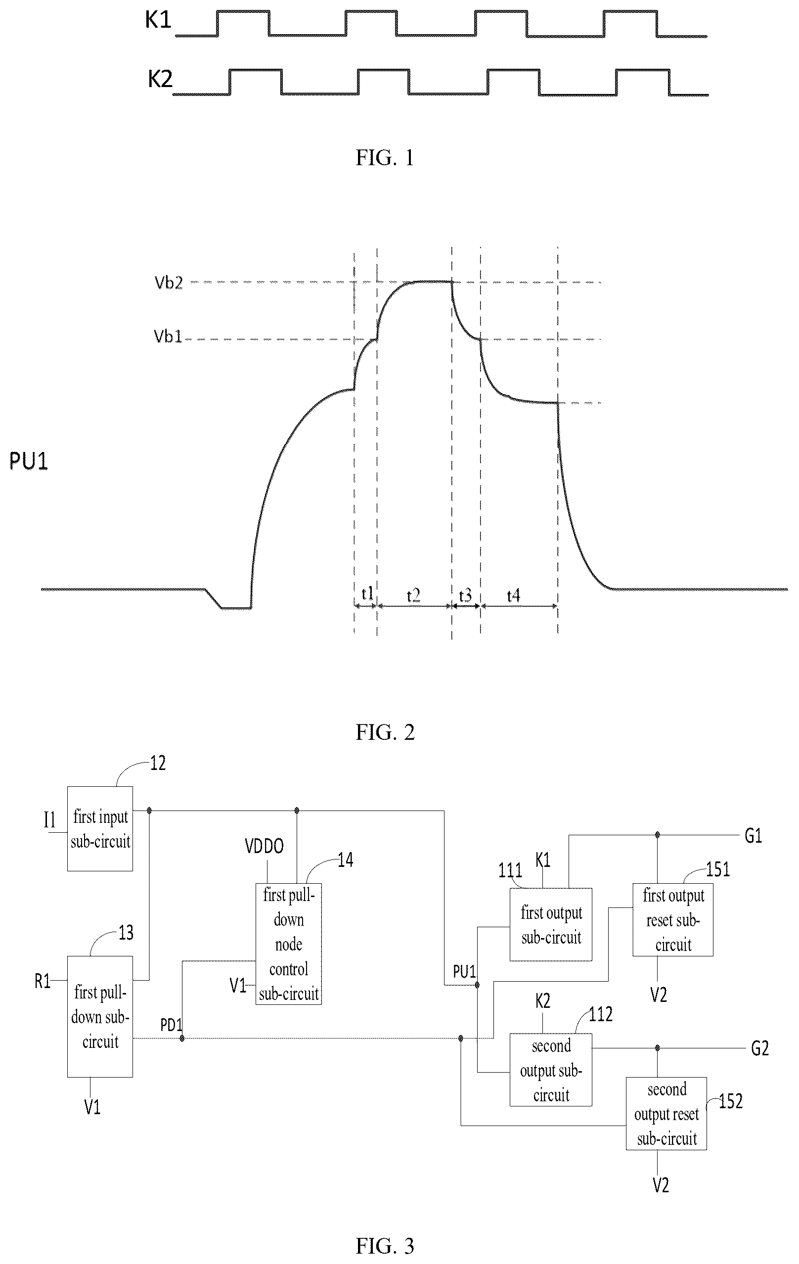
1 . A display driving circuit, comprising two gate driving circuits, wherein the two gate driving circuits are respectively arranged on two opposite sides of a display panel; the gate driving circuit includes a plurality of cascaded driving circuits; the driving circuit includes N clock signal terminals, N output sub-circuits and N driving signal output terminals; N is an integer greater than or equal to 2; the N output sub-circuits share a first pull-up node; an nth output sub-circuit is used to control to output an nth driving signal through an nth driving signal output terminal according to an nth clock signal provided by an nth clock signal terminal under the control of a potential of the first pull-up node; n is a positive integer less than or equal to N; an ith driving signal output terminal of one of the two driving circuits is electrically connected to an (i+j)th driving signal output terminal of the other of the two driving circuits, and both i and j are positive integers, i is a positive integer less than or equal to N, j is a positive integer less than or equal to N, and i+j is a positive integer less than or equal to N; when a potential of an ith clock signal provided by the ith clock signal terminal among the N clock signal terminals jumps from an invalid level to a valid level, the potential of the first pull-up node is a first voltage value, when a potential of an (i+j)th clock signal provided by the (i+j)th clock signal terminal among the N clock signal terminals jumps from an invalid level to a valid level, the potential of the first pull-up node is a second voltage value; the first voltage value is not equal to the second voltage value; a time period during which the potential of the ith clock signal continues to be at the valid level and a time period during which the potential of the (i+j)th clock signal continues to be at the valid level at least partially overlap; a time point when the potential of the ith clock signal jumps from the valid level to the invalid level is different from a time point when the potential of the (i+j)th clock signal jumps from the valid level to the invalid level; wherein the driving circuit further includes a first input sub-circuit, a first pull-down sub-circuit, a first pull-down node control sub-circuit, and N output reset sub-circuits; the N output reset sub-circuits share the first pull-down node; the first input sub-circuit is configured to control the potential of the first pull-up node under the control of a first input signal provided by the first input terminal; the first pull-down sub-circuit is electrically connected to the first pull-up node, the first pull-down node, a first reset terminal and the first voltage terminal respectively, and is used to control to connect the first pull-up node and the first voltage terminal under the control of the potential of the first pull-down node, and control to connect the first pull-up node and the first voltage terminal under the control of a first reset signal provided by the first reset terminal; the first pull-down node control sub-circuit is electrically connected to a first control voltage terminal, the first pull-up node, the first pull-down node and the first voltage terminal, and is configured to control the potential of the first pull-down node under the control of a first control voltage provided by the first control voltage terminal and the potential of the first pull-up node, according to a first voltage signal provided by the first voltage terminal; an nth output reset sub-circuit is electrically connected to the first pull-down node, a second voltage terminal, and an nth driving signal output terminal, and is used to control to connect the nth driving signal output terminal and the second voltage terminal under the control of the potential of the first pull-down node.
Show 18 dependent claims
2 . The display driving circuit according to claim 1 , wherein when the potential of the ith clock signal jumps from the valid level to the invalid level, the potential of the first pull-up node is a third voltage value; when the potential of the (i+j)th clock signal jumps from the valid level to the invalid level, the potential of the first pull-up node is a fourth voltage value; the third voltage value is not equal to the fourth voltage value.
3 . The display driving circuit according to claim 1 , wherein when the potential of the ith clock signal jumps from the invalid level to the valid level, within a first time period, the potential of the first pull-up node rises by a first potential height; when the potential of the (i+j)th clock signal jumps from the invalid level to the valid level, within a second time, the potential of the first pull-up node rises by a second potential height; the first potential height is not equal to the second potential height, and/or, the first time is not equal to the second time.
4 . The display driving circuit according to claim 3 , wherein the driving circuit includes a capacitor arranged between an ath driving signal terminal and the first pull-up node, the first time is less than the second time, and the first potential height is smaller than the second potential height; a is an even number, and a is a positive integer; or; the driving circuit includes a capacitor arranged between a bth driving signal terminal and the first pull-up node, the first time is greater than the second time, and the first potential height is greater than the second potential height; b is an odd number, and b is a positive integer.
5 . The display driving circuit according to claim 1 , wherein when the potential of the ith clock signal jumps from the valid level to the invalid level, within a third time period, the potential of the first pull-up node drops by a third potential height; when the potential of the (i+j)th clock signal jumps from the valid level to the invalid level, within a fourth time, the potential of the first pull-up node drops by a fourth potential height; the third potential height is not equal to the fourth potential height, and/or, the third time is not equal to the fourth time.
6 . The display driving circuit according to claim 5 , wherein the driving circuit includes a capacitor arranged between the ath driving signal terminal and the first pull-up node, the third time is less than the fourth time, and the third potential height is greater than the fourth potential height; a is an even number, and a is a positive integer; or; the driving circuit includes a capacitor arranged between the bth driving signal terminal and the first pull-up node, the third time is greater than the fourth time, and the third potential height is less than the fourth potential height; b is an odd number, and b is a positive integer.
7 . The display driving circuit according to claim 1 , wherein the driving circuit further includes a first carry signal output terminal and a first carry output sub-circuit; the first carry output sub-circuit is electrically connected to the first pull-up node, the first carry signal output terminal and a first carry clock signal terminal respectively, and is configured to control to connect the first carry signal output terminal and the first carry clock signal terminal under the control of the potential of the first pull-up node, wherein the first input sub-circuit is respectively electrically connected to the first input terminal, the first input voltage terminal and the first pull-up node, is configured to control to connect the first pull-up node and the first input voltage terminal under the control of the first input signal provided by the first input terminal; the first input terminal is a first carry signal output terminal of an adjacent previous stage of driving circuit; the first input voltage terminal is a first carry signal output terminal of the adjacent previous stage of driving circuit, a cth driving signal output terminal included in the adjacent previous stage of driving circuit or a third voltage terminal; c is a positive integer less than or equal to N.
8 . The display driving circuit according to claim 7 , wherein the nth output sub-circuit comprises an nth output transistor; a control electrode of the nth output transistor is electrically connected to the first pull-up node, a first electrode of the nth output transistor is electrically connected to the nth clock signal terminal, and a second electrode of the nth output transistor is electrically connected to the nth driving signal output terminal; the first carry output sub-circuit includes a first carry output transistor; a control electrode of the first carry output transistor is electrically connected to the first pull-up node, a first electrode of the first carry output transistor is electrically connected to the first carry clock signal terminal, and a second electrode of the first carry output transistor is electrically connected to the first carry signal output terminal; the nth output reset sub-circuit includes an nth output reset transistor; a control electrode of the nth output reset transistor is electrically connected to the first pull-down node, a first electrode of the nth output reset transistor is electrically connected to the nth driving signal output terminal, and a second electrode of the nth output reset transistor is electrically connected to the second voltage terminal.
9 . The display driving circuit according to claim 8 , wherein the driving circuit further comprises a first on-off control sub-circuit; the first on-off control sub-circuit is electrically connected to a touch enable terminal, a first connection node and the first pull-up node respectively, and is configured to control to connect or disconnect the first connection node and the first pull-up node under the control of a touch enable signal provided by the touch enable terminal, wherein the first on-off control sub-circuit comprises a first on-off control transistor; a control electrode of the first on-off control transistor is electrically connected to the touch enable terminal, a first electrode of the first on-off control transistor is connected to the first pull-up node, and a second electrode of the first on-off control transistor is electrically connected to the first connection node.
10 . The display driving circuit according to claim 1 , wherein the driving circuit further comprises N capacitors; a first terminal of an nth capacitor among the N capacitors is electrically connected to the first pull-up node, and a second terminal of the nth capacitor among the N capacitors is electrically connected to the nth driving signal output terminal.
11 . The display driving circuit according to claim 1 , wherein the driving circuit further includes M clock signal terminals, M output sub-circuits, a second carry output sub-circuit, M driving signal output terminals and a second carry signal output terminal; the M output sub-circuits share a second pull-up node; an (N+m)th output sub-circuit is configured to output an (N+m)th driving signal through an (N+m)th driving signal output terminal according to an (N+m)th clock signal provided by the (N+m)th clock signal terminal under the control of a potential of the second pull-up node, m is a positive integer less than or equal to M, and M is a positive integer greater than or equal to 2; the second carry output sub-circuit is electrically connected to the second pull-up node, the second carry signal output terminal and the second carry clock signal terminal, and is configured to control to connect the second carry signal output terminal and the second carry clock signal terminal under the control of the potential of the second pull-up node.
12 . The display driving circuit according to claim 11 , wherein the driving circuit further comprises M capacitors; a first terminal of an mth capacitor among the M capacitors is electrically connected to the second pull-up node, and a second terminal of the mth capacitor among the M capacitors is connected to the (N+m)th driving signal output terminal.
13 . The display driving circuit according to claim 11 , wherein the driving circuit further includes a second input sub-circuit, a second pull-down sub-circuit, a second pull-down node control sub-circuit, and M output reset sub-circuits; the M output reset sub-circuits share a second pull-down node; the second input sub-circuit is configured to control the potential of the second pull-up node under the control of a second input signal provided by the second input terminal; the second pull-down sub-circuit is respectively electrically connected to the second pull-up node, the second pull-down node, the second reset terminal and the first voltage terminal, and is used to control to connect the second pull-up node and the first voltage terminal under the control of a potential of the second pull-down node, and control to connect the second pull-up node and the first voltage terminal under the control of a second reset signal provided by the second reset terminal; the second pull-down node control sub-circuit is electrically connected to a second control voltage terminal, the second pull-up node, the second pull-down node, and the first voltage terminal, is configured to control the potential of the second pull-down node under the control of a second control voltage provided by the second control voltage terminal and the potential of the second pull-up node according to the first voltage signal provided by the first voltage terminal; the (N+m)th output reset sub-circuit is electrically connected to the second pull-down node, the second voltage terminal, and the (N+m)th driving signal output terminal, and is used to control to connect the (N+m)th driving signal output terminal and the second voltage terminal under the control of the potential of the second pull-down node.
14 . The display driving circuit according to claim 13 , wherein the driving circuit further comprises a second carry reset sub-circuit; the second carry reset sub-circuit is electrically connected to the second pull-down node, the second carry signal output terminal and the first voltage terminal, and is used to control to connect the second carry signal output terminal and the first voltage terminal under the control of the potential of the second pull-down node, wherein the second carry reset sub-circuit comprises a third carry reset transistor and a fourth carry reset transistor; a control electrode of the third carry reset transistor is electrically connected to the second pull-down node, a first electrode of the third carry reset transistor is electrically connected to the second carry signal output terminal, and a second electrode of the third carry reset transistor is electrically connected to the first voltage terminal; a control electrode of the fourth carry reset transistor is electrically connected to the first pull-down node, a first electrode of the fourth carry reset transistor is electrically connected to the second carry signal output terminal, and a second electrode of the fourth carry reset transistor is electrically connected to the first voltage terminal.
15 . The display driving circuit according to claim 13 , wherein the second input sub-circuit is respectively electrically connected to the second input terminal, the second input voltage terminal and the second pull-up node, is configured to control to connect the second pull-up node and the second input voltage terminal under the control of the second input signal provided by the second input terminal; the second input terminal is a second carry signal output terminal of an adjacent previous stage of driving circuit; the second input voltage terminal is the second carry signal output terminal of the adjacent previous stage of driving circuit, a dth driving signal output terminal included in the adjacent previous stage of driving circuit or the third voltage terminal; d is a positive integer less than or equal to M, wherein the second carry clock signal terminal is a dth clock signal terminal among the M clock signal terminals; the second pull-down sub-circuit is further electrically connected to the second input voltage terminal, and is used to control to connect the second pull-down node and the first voltage terminal under the control of the second input voltage provided by the second input voltage terminal; the second input sub-circuit is also electrically connected to the frame reset terminal, and is also used to control to connect the second pull-up node and the first voltage terminal under the control of the frame reset signal provided by the frame reset terminal.
16 . The display driving circuit according to claim 13 , wherein the second pull-down sub-circuit comprises a twelfth transistor; a control electrode of the twelfth transistor is electrically connected to the first pull-down node, a first electrode of the twelfth transistor is electrically connected to the second pull-up node, and a second electrode of the twelfth transistor is electrically connected to the first voltage terminal; the second pull-down node control sub-circuit includes a thirteenth transistor; a control electrode of the thirteenth transistor is electrically connected to the first pull-up node, a first electrode of the thirteenth transistor is electrically connected to the second pull-down control node, and a second electrode of the thirteenth transistor is electrically connected to the first voltage terminal.
17 . The display driving circuit according to claim 13 , wherein the driving circuit further comprises a second on-off control sub-circuit; the second on-off control sub-circuit is electrically connected to a touch enable terminal, a second connection node and the second pull-up node, and is configured to control to connect or disconnect the second connection node and the second pull-up node under the control of a touch enable signal provided by the touch enable terminal.
18 . The display driving circuit according to claim 1 , wherein the first pull-down sub-circuit further comprises a tenth transistor; a control electrode of the tenth transistor is electrically connected to the second pull-down node, a first electrode of the tenth transistor is electrically connected to the first pull-up node, and a second electrode of the tenth transistor is electrically connected to the first voltage terminal; the first pull-down node control sub-circuit further includes an eleventh transistor; a control electrode of the eleventh transistor is electrically connected to the second pull-up node, a first electrode of the eleventh transistor is electrically connected to the first pull-down control node, and a second electrode of the eleventh transistor is electrically connected to the first voltage terminal.
19 . A display device comprising the display driving circuit according to claim 1 .
Full Description
Show full text →
CROSS REFERENCE TO RELATED APPLICATION
The present disclosure is the U.S. national phase of PCT Application No. PCT/CN2022/102548 filed on Jun. 29, 2022, which are incorporated herein by reference in their entireties.
TECHNICAL FIELD
The present disclosure relates to the field of display technology, in particular to a display driving circuit and a display device.
BACKGROUND
Related display products are designed using a bilaterally symmetrical Gate On Array (GOA, gate driving circuit on the array substrate) model design, which is difficult to achieve the narrow frame. For full screens and increasingly stringent product frames, wiring space are severely restricted, and it is difficult to meet the product requirements of high resolution and high refresh rate.
SUMMARY
In one aspect, the present disclosure provides in some embodiments a display driving circuit, including two gate driving circuits, wherein the two gate driving circuits are respectively arranged on two opposite sides of a display panel; the gate driving circuit includes a plurality of cascaded driving circuits; the driving circuit includes N clock signal terminals, N output sub-circuits and N driving signal output terminals; N is an integer greater than or equal to 2; the N output sub-circuits share a first pull-up node; an nth output sub-circuit is used to control to output an nth driving signal through an nth driving signal output terminal according to an nth clock signal provided by an nth clock signal terminal under the control of a potential of the first pull-up node; n is a positive integer less than or equal to N; an ith driving signal output terminal of one of the two driving circuits is electrically connected to an (i+j)th driving signal output terminal of the other of the two driving circuits, and both i and j are positive integers, i is a positive integer less than or equal to N, j is a positive integer less than or equal to N, and i+j is a positive integer less than or equal to N; when a potential of an ith clock signal provided by the ith clock signal terminal among the N clock signal terminals jumps from an invalid level to a valid level, the potential of the first pull-up node is a first voltage value, when a potential of an (i+j)th clock signal provided by the (i+j)th clock signal terminal among the N clock signal terminals jumps from an invalid level to a valid level, the potential of the first pull-up node is a second voltage value; the first voltage value is not equal to the second voltage value; a time period during which the potential of the ith clock signal continues to be at the valid level and a time period during which the potential of the (i+j)th clock signal continues to be at the valid level at least partially overlap; a time point when the potential of the ith clock signal jumps from the valid level to the invalid level is different from a time point when the potential of the (i+j)th clock signal jumps from the valid level to the invalid level. Optionally, when the potential of the ith clock signal jumps from the valid level to the invalid level, the potential of the first pull-up node is a third voltage value; when the potential of the (i+j)th clock signal jumps from the valid level to the invalid level, the potential of the first pull-up node is a fourth voltage value; the third voltage value is not equal to the fourth voltage value. Optionally, when the potential of the ith clock signal jumps from the invalid level to the valid level, within a first time period, the potential of the first pull-up node rises by a first potential height; when the potential of the (i+j)th clock signal jumps from the invalid level to the valid level, within a second time, the potential of the first pull-up node rises by a second potential height; the first potential height is not equal to the second potential height, and/or, the first time is not equal to the second time. Optionally, when the potential of the ith clock signal jumps from the valid level to the invalid level, within a third time period, the potential of the first pull-up node drops by a third potential height; when the potential of the (i+j)th clock signal jumps from the valid level to the invalid level, within a fourth time, the potential of the first pull-up node drops by a fourth potential height; the third potential height is not equal to the fourth potential height, and/or, the third time is not equal to the fourth time. Optionally, the driving circuit includes a capacitor arranged between an ath driving signal terminal and the first pull-up node, the first time is less than the second time, and the first potential height is smaller than the second potential height; a is an even number, and a is a positive integer; or; the driving circuit includes a capacitor arranged between a bth driving signal terminal and the first pull-up node, the first time is greater than the second time, and the first potential height is greater than the second potential height; b is an odd number, and b is a positive integer. Optionally, the driving circuit includes a capacitor arranged between the ath driving signal terminal and the first pull-up node, the third time is less than the fourth time, and the third potential height is greater than the fourth potential height; a is an even number, and a is a positive integer; or; the driving circuit includes a capacitor arranged between the bth driving signal terminal and the first pull-up node, the third time is greater than the fourth time, and the third potential height is less than the fourth potential height; b is an odd number, and b is a positive integer. Optionally, the driving circuit further includes a first input sub-circuit, a first pull-down sub-circuit, a first pull-down node control sub-circuit, and N output reset sub-circuits; the N output reset sub-circuits share the first pull-down node; the first input sub-circuit is configured to control the potential of the first pull-up node under the control of a first input signal provided by the first input terminal; the first pull-down sub-circuit is electrically connected to the first pull-up node, the first pull-down node, a first reset terminal and the first voltage terminal respectively, and is used to control to connect the first pull-up node and the first voltage terminal under the control of the potential of the first pull-down node, and control to connect the first pull-up node and the first voltage terminal under the control of a first reset signal provided by the first reset terminal; the first pull-down node control sub-circuit is electrically connected to a first control voltage terminal, the first pull-up node, the first pull-down node and the first voltage terminal, and is configured to control the potential of the first pull-down node under the control of a first control voltage provided by the first control voltage terminal and the potential of the first pull-up node, according to a first voltage signal provided by the first voltage terminal; an nth output reset sub-circuit is electrically connected to the first pull-down node, a second voltage terminal, and an nth driving signal output terminal, and is used to control to connect the nth driving signal output terminal and the second voltage terminal under the control of the potential of the first pull-down node. Optionally, the driving circuit further includes a first carry signal output terminal and a first carry output sub-circuit; the first carry output sub-circuit is electrically connected to the first pull-up node, the first carry signal output terminal and a first carry clock signal terminal respectively, and is configured to control to connect the first carry signal output terminal and the first carry clock signal terminal under the control of the potential of the first pull-up node. Optionally, the driving circuit further comprises a first carry reset sub-circuit; the first carry reset sub-circuit is electrically connected to the first pull-down node, the first carry signal output terminal and the first voltage terminal, and is used to control to connect the first carry signal output terminal and the first voltage terminal under the control of the potential of the first pull-down node. Optionally, the first input sub-circuit is respectively electrically connected to the first input terminal, the first input voltage terminal and the first pull-up node, is configured to control to connect the first pull-up node and the first input voltage terminal under the control of the first input signal provided by the first input terminal; the first input terminal is a first carry signal output terminal of an adjacent previous stage of driving circuit; the first input voltage terminal is a first carry signal output terminal of the adjacent previous stage of driving circuit, a cth driving signal output terminal included in the adjacent previous stage of driving circuit or a third voltage terminal; c is a positive integer less than or equal to N. Optionally, the first carry clock signal terminal is a cth clock signal terminal among the N clock signal terminals; the first pull-down sub-circuit is electrically connected to the first input voltage terminal, is configured to control to connect the first pull-down node and the first voltage terminal under the control of the first input voltage provided by the first input voltage terminal; the first input sub-circuit is also electrically connected to a frame reset terminal, is configured to control to connect the first pull-up node and the first voltage terminal under the control of a frame reset signal provided by the frame reset terminal. Optionally, the driving circuit further comprises N capacitors; a first terminal of an nth capacitor among the N capacitors is electrically connected to the first pull-up node, and a second terminal of the nth capacitor among the N capacitors is electrically connected to the nth driving signal output terminal. Optionally, the first input sub-circuit includes a first transistor, the first pull-down sub-circuit includes a second transistor and a third transistor; the first pull-down node control sub-circuit includes a fourth transistor, a fifth a transistor, a sixth transistor and a seventh transistor; a control electrode of the first transistor is electrically connected to the first input terminal, a first electrode of the first transistor is electrically connected to the first input voltage terminal, and a second electrode of the first transistor is electrically connected to the first pull-up node; a control electrode of the second transistor is electrically connected to the first reset terminal, a first electrode of the second transistor is electrically connected to the first pull-up node, and a second electrode of the second transistor is electrically connected to the first voltage terminal; a control electrode of the third transistor is electrically connected to the first pull-down node, a first electrode of the third transistor is electrically connected to the first pull-up node, and a second electrode of the third transistor is electrically connected to the first voltage terminal; both a control electrode of the fourth transistor and a first electrode of the fourth transistor are electrically connected to the first control voltage terminal, and a second electrode of the fourth transistor is electrically connected to the first pull-down control node; a control electrode of the fifth transistor is electrically connected to the first pull-down control node, a first electrode of the fifth transistor is electrically connected to the first control voltage terminal, and a second electrode of the fifth transistor is electrically connected to the first pull-down node; a control electrode of the sixth transistor is electrically connected to the first pull-up node, a first electrode of the sixth transistor is electrically connected to the first pull-down node, and a second electrode of the sixth transistor is electrically connected to the first voltage terminal; a control electrode of the seventh transistor is electrically connected to the first pull-up node, a first electrode of the seventh transistor is electrically connected to the first pull-down control node, and a second electrode of the seventh transistor is electrically connected to the first voltage terminal. Optionally, the first pull-down sub-circuit includes an eighth transistor, and the first input sub-circuit further includes a ninth transistor; a control electrode of the eighth transistor is electrically connected to the first input voltage terminal, a first electrode of the eighth transistor is electrically connected to the first pull-down node, and a second electrode of the eighth transistor is electrically connected to the first voltage terminal; a control electrode of the ninth transistor is electrically connected to the frame reset terminal, a first electrode of the ninth transistor is electrically connected to the first pull-up node, and a second electrode of the ninth transistor is electrically connected to the first voltage terminal. Optionally, the nth output sub-circuit comprises an nth output transistor; a control electrode of the nth output transistor is electrically connected to the first pull-up node, a first electrode of the nth output transistor is electrically connected to the nth clock signal terminal, and a second electrode of the nth output transistor is electrically connected to the nth driving signal output terminal; the first carry output sub-circuit includes a first carry output transistor; a control electrode of the first carry output transistor is electrically connected to the first pull-up node, a first electrode of the first carry output transistor is electrically connected to the first carry clock signal terminal, and a second electrode of the first carry output transistor is electrically connected to the first carry signal output terminal; the nth output reset sub-circuit includes an nth output reset transistor; a control electrode of the nth output reset transistor is electrically connected to the first pull-down node, a first electrode of the nth output reset transistor is electrically connected to the nth driving signal output terminal, and a second electrode of the nth output reset transistor is electrically connected to the second voltage terminal. Optionally, the first carry reset sub-circuit comprises a first carry reset transistor; a control electrode of the first carry reset transistor is electrically connected to the first pull-down node, a first electrode of the first carry reset transistor is electrically connected to the first carry signal output terminal, and a second electrode of the first carry reset transistor is electrically connected to the first voltage terminal. Optionally, the driving circuit further comprises a first on-off control sub-circuit; the first on-off control sub-circuit is electrically connected to a touch enable terminal, a first connection node and the first pull-up node respectively, and is configured to control to connect or disconnect the first connection node and the first pull-up node under the control of a touch enable signal provided by the touch enable terminal. Optionally, the first on-off control sub-circuit comprises a first on-off control transistor; a control electrode of the first on-off control transistor is electrically connected to the touch enable terminal, a first electrode of the first on-off control transistor is connected to the first pull-up node, and a second electrode of the first on-off control transistor is electrically connected to the first connection node. Optionally, the driving circuit further comprises a first output capacitor; a first terminal of the first output capacitor is electrically connected to the pull-up node circuit, and a second terminal of the first output capacitor is electrically connected to one of the N driving signal output terminals. Optionally, the driving circuit further includes M clock signal terminals, M output sub-circuits, a second carry output sub-circuit, M driving signal output terminals and a second carry signal output terminal; the M output sub-circuits share a second pull-up node; an (N+m)th output sub-circuit is configured to output an (N+m)th driving signal through an (N+m)th driving signal output terminal according to an (N+m)th clock signal provided by the (N+m)th clock signal terminal under the control of a potential of the second pull-up node, m is a positive integer less than or equal to M, and M is a positive integer greater than or equal to 2; the second carry output sub-circuit is electrically connected to the second pull-up node, the second carry signal output terminal and the second carry clock signal terminal, and is configured to control to connect the second carry signal output terminal and the second carry clock signal terminal under the control of the potential of the second pull-up node. Optionally, the driving circuit further comprises M capacitors; a first terminal of an mth capacitor among the M capacitors is electrically connected to the second pull-up node, and a second terminal of the mth capacitor among the M capacitors is connected to the (N+m)th driving signal output terminal. Optionally, the driving circuit further includes a second input sub-circuit, a second pull-down sub-circuit, a second pull-down node control sub-circuit, and M output reset sub-circuits; the M output reset sub-circuits share a second pull-down node; the second input sub-circuit is configured to control the potential of the second pull-up node under the control of a second input signal provided by the second input terminal; the second pull-down sub-circuit is respectively electrically connected to the second pull-up node, the second pull-down node, the second reset terminal and the first voltage terminal, and is used to control to connect the second pull-up node and the first voltage terminal under the control of a potential of the second pull-down node, and control to connect the second pull-up node and the first voltage terminal under the control of a second reset signal provided by the second reset terminal; the second pull-down node control sub-circuit is electrically connected to a second control voltage terminal, the second pull-up node, the second pull-down node, and the first voltage terminal, is configured to control the potential of the second pull-down node under the control of a second control voltage provided by the second control voltage terminal and the potential of the second pull-up node according to the first voltage signal provided by the first voltage terminal; the (N+m)th output reset sub-circuit is electrically connected to the second pull-down node, the second voltage terminal, and the (N+m)th driving signal output terminal, and is used to control to connect the (N+m)th driving signal output terminal and the second voltage terminal under the control of the potential of the second pull-down node. Optionally, the driving circuit further comprises a second carry reset sub-circuit; the second carry reset sub-circuit is electrically connected to the second pull-down node, the second carry signal output terminal and the first voltage terminal, and is used to control to connect the second carry signal output terminal and the first voltage terminal under the control of the potential of the second pull-down node. Optionally, the second input sub-circuit is respectively electrically connected to the second input terminal, the second input voltage terminal and the second pull-up node, is configured to control to connect the second pull-up node and the second input voltage terminal under the control of the second input signal provided by the second input terminal; the second input terminal is a second carry signal output terminal of an adjacent previous stage of driving circuit; the second input voltage terminal is the second carry signal output terminal of the adjacent previous stage of driving circuit, a dth driving signal output terminal included in the adjacent previous stage of driving circuit or the third voltage terminal; d is a positive integer less than or equal to M. Optionally, the second carry clock signal terminal is a dth clock signal terminal among the M clock signal terminals; the second pull-down sub-circuit is further electrically connected to the second input voltage terminal, and is used to control to connect the second pull-down node and the first voltage terminal under the control of the second input voltage provided by the second input voltage terminal; the second input sub-circuit is also electrically connected to the frame reset terminal, and is also used to control to connect the second pull-up node and the first voltage terminal under the control of the frame reset signal provided by the frame reset terminal. Optionally, the driving circuit further comprises M capacitors; a first terminal of an mth capacitor among the M capacitors is electrically connected to the second pull-up node, and a second terminal of the mth capacitor among the M capacitors is connected to the (N+m)th driving signal output terminal. Optionally, the first pull-down sub-circuit further comprises a tenth transistor; a control electrode of the tenth transistor is electrically connected to the second pull-down node, a first electrode of the tenth transistor is electrically connected to the first pull-up node, and a second electrode of the tenth transistor is electrically connected to the first voltage terminal; the first pull-down node control sub-circuit further includes an eleventh transistor; a control electrode of the eleventh transistor is electrically connected to the second pull-up node, a first electrode of the eleventh transistor is electrically connected to the first pull-down control node, and a second electrode of the eleventh transistor is electrically connected to the first voltage terminal. Optionally, the nth output reset sub-circuit further comprises an nth reset transistor; a control electrode of the nth reset transistor is electrically connected to the second pull-down node, a first electrode of the nth reset transistor is electrically connected to the nth driving signal output terminal, and a second electrode of the nth reset transistor is electrically connected to the second voltage terminal. Optionally, the first carry reset sub-circuit further comprises a second carry reset transistor; a control electrode of the second carry reset transistor is electrically connected to the second pull-down node, a first electrode of the second carry reset transistor is electrically connected to the first carry signal output terminal, and a second electrode of the second carry reset transistor is electrically connected to the first voltage terminal. Optionally, the second pull-down sub-circuit comprises a twelfth transistor; a control electrode of the twelfth transistor is electrically connected to the first pull-down node, a first electrode of the twelfth transistor is electrically connected to the second pull-up node, and a second electrode of the twelfth transistor is electrically connected to the first voltage terminal; the second pull-down node control sub-circuit includes a thirteenth transistor; a control electrode of the thirteenth transistor is electrically connected to the first pull-up node, a first electrode of the thirteenth transistor is electrically connected to the second pull-down control node, and a second electrode of the thirteenth transistor is electrically connected to the first voltage terminal. Optionally, the (N+m)th output reset sub-circuit comprises an (N+m)th reset transistor; a control electrode of the (N+m)th reset transistor is electrically connected to the first pull-down node, a first electrode of the (N+m)th reset transistor is electrically connected to the (N+m)th driving signal output terminal, and a second electrode of the (N+m)th reset transistor is electrically connected to the second voltage terminal. Optionally, the second carry reset sub-circuit comprises a third carry reset transistor and a fourth carry reset transistor; a control electrode of the third carry reset transistor is electrically connected to the second pull-down node, a first electrode of the third carry reset transistor is electrically connected to the second carry signal output terminal, and a second electrode of the third carry reset transistor is electrically connected to the first voltage terminal; a control electrode of the fourth carry reset transistor is electrically connected to the first pull-down node, a first electrode of the fourth carry reset transistor is electrically connected to the second carry signal output terminal, and a second electrode of the fourth carry reset transistor is electrically connected to the first voltage terminal. Optionally, the driving circuit further comprises a second on-off control sub-circuit; the second on-off control sub-circuit is electrically connected to a touch enable terminal, a second connection node and the second pull-up node, and is configured to control to connect or disconnect the second connection node and the second pull-up node under the control of a touch enable signal provided by the touch enable terminal. Optionally, the second on-off control sub-circuit comprises a second on-off control transistor; a control electrode of the second on-off control transistor is electrically connected to the touch enable terminal, a first electrode of the second on-off control transistor is connected to the second pull-up node, and a second electrode of the second on-off control transistor is electrically connected to the second connection node. Optionally, the display driving includes a second output capacitor; a first terminal of the second output capacitor is electrically connected to the second pull-up node, and a second terminal of the second output capacitor is electrically connected to one of the M driving signal output terminals. In a second aspect, an embodiment of the present disclosure provides a display device comprising the display driving circuit. Optionally, the display device further includes a plurality of rows of gate lines, a plurality of columns of data lines, and a plurality of rows and a plurality of columns of pixel circuits; wherein the pixel circuit includes a display control transistor and a pixel electrode; a gate electrode of the display control transistor is electrically connected to the gate line, a first electrode of the display control transistor is electrically connected to the data line, and a second electrode of the display control transistor is electrically connected to the pixel electrode; the pixel electrode has a plurality of slits; an angle between slit directions of two pixel electrodes included in a same pixel electrode group is greater than 90 degrees and less than 180 degrees; the pixel electrode group is arranged in a display area formed by adjacent rows of gate lines and adjacent columns of data lines. Optionally, two rows of gate lines are arranged between two rows of adjacent pixel electrodes; a gate electrode of one of the two transistors electrically connected to a same column of data line is electrically connected to one of the two rows of gate lines, and a gate electrode of the other of the two transistor electrically connected to the same column of data lines is electrically connected to the other of the two rows of gate lines; a width along a first direction of a conductive connection portion between the two transistors electrically connected to the same column of data line and the column of data line is greater than a minimum width of the data line along the first direction; the first direction is an extending direction of the gate lines. Optionally, the display device further includes a plurality of rows and a plurality of columns of common electrodes; wherein two adjacent rows of common electrodes are electrically connected by a crossing line, and the crossing line is arranged on a same layer as the pixel electrode. Optionally, pixel electrodes corresponding to two ends of the crossing line have an avoiding portion. Optionally, a line width of the gate line is smaller than a maximum line width of the gate line at an overlapping position between the crossing line and the gate line.
BRIEF DESCRIPTION OF THE DRAWINGS
is a waveform diagram of a first clock signal and a second clock signal; is a waveform diagram of the potential of the first pull-up node; is a structural diagram of a driving circuit in a display driving circuit according to at least one embodiment of the present disclosure; is a structural diagram of the driving circuit according to at least embodiment; is a structural diagram of the driving circuit according to at least embodiment; is a structural diagram of the driving circuit according to at least embodiment; is a structural diagram of the driving circuit according to at least embodiment; is a circuit diagram of the driving circuit according to at least embodiment; is a working timing diagram of the driving circuit shown in ; is a circuit diagram of the driving circuit according to at least embodiment; is a waveform diagram of the potential of the first pull-up node PU 1 when the driving circuit shown in is in operation according to at least one embodiment of the present disclosure; is a circuit diagram of the driving circuit according to at least one embodiment of the present disclosure; is a circuit diagram of the driving circuit according to at least one embodiment of the present disclosure; is a circuit diagram of the driving circuit according to at least one embodiment of the present disclosure; is a circuit diagram of the driving circuit according to at least one embodiment of the present disclosure; is a circuit diagram of the driving circuit according to at least one embodiment of the present disclosure; is a circuit diagram of the driving circuit according to at least one embodiment of the present disclosure; is a circuit diagram of the driving circuit according to at least one embodiment of the present disclosure; is a circuit diagram of the driving circuit according to at least one embodiment of the present disclosure; is a circuit diagram of the driving circuit according to at least one embodiment of the present disclosure; is a circuit diagram of the driving circuit according to at least one embodiment of the present disclosure; is a circuit diagram of the driving circuit according to at least one embodiment of the present disclosure; is a circuit diagram of the driving circuit according to at least one embodiment of the present disclosure; is a circuit diagram of the driving circuit according to at least one embodiment of the present disclosure; is a circuit diagram of the driving circuit according to at least one embodiment of the present disclosure; is a working timing diagram of the driving circuit shown in ; is a circuit diagram of the driving circuit according to at least one embodiment of the present disclosure; is a circuit diagram of the driving circuit according to at least one embodiment of the present disclosure; is a structural diagram of a display driving circuit according to at least one embodiment of the present disclosure; is a waveform diagram of ten clock signals; is a structural diagram of a display driving circuit according to at least one embodiment of the present disclosure; is a structural diagram of a part of a display driving circuit according to at least one embodiment of the present disclosure; is a structural diagram of a part of a display driving circuit according to at least one embodiment of the present disclosure; is a structural diagram of a display substrate in a display device according to at least one embodiment of the present disclosure; A, 35 B and 35 C are layout diagrams of a display substrate including pixel circuits shown in according to at least embodiment of the present disclosure; is a layout diagram of the common electrode, the gate electrodes of display control transistor and each gate line in B ; is a layout diagram of the data line, the source electrode of each display control transistor, the drain electrode of each display control transistor, and the active layer of each display control transistor in B ; is a layout diagram of pixel electrodes and crossing lines in B .
DETAILED DESCRIPTION
The following will clearly and completely describe the technical solutions in the embodiments of the present disclosure with reference to the accompanying drawings. Apparently, the described embodiments are only some of the embodiments of the present disclosure, not all of them. Based on the embodiments in the present disclosure, all other embodiments obtained by persons of ordinary skill in the art without making creative efforts belong to the protection scope of the present disclosure. The transistors used in all the embodiments of the present disclosure may be triodes, thin film transistors or field effect transistors or other devices with the same characteristics. In the embodiments of the present disclosure, in order to distinguish the two electrodes of the transistor except the control electrode, one electrode is called the first electrode, and the other electrode is called the second electrode. In actual operation, when the transistor is a triode, the control electrode can be a base, the first electrode can be a collector, and the second electrode can be an emitter; or, the control electrode can be a base electrode, the first electrode may be an emitter, and the second electrode may be a collector. In actual operation, when the transistor is a thin film transistor or a field effect transistor, the control electrode may be a gate electrode, the first electrode may be a drain electrode, and the second electrode may be a source electrode; or, the control electrode may be a gate electrode, the first electrode may be a source electrode, and the second electrode may be a drain electrode. The display driving circuit described in the embodiment of the present disclosure includes two gate driving circuits, and the two gate driving circuits are respectively arranged on opposite sides of the display panel; the gate driving circuit includes a plurality of cascaded driving circuits; The driving circuit includes N clock signal terminals, N output sub-circuits and N driving signal output terminals; N is an integer greater than or equal to 2; the N output sub-circuits share a first pull-up node; The nth output sub-circuit is used to control to output an nth driving signal through an nth driving signal output terminal according to an nth clock signal provided by an nth clock signal terminal under the control of a potential of the first pull-up node; n is a positive integer less than or equal to N; An ith driving signal output terminal of one of the two driving circuits is electrically connected to an (i+j)th driving signal output terminal of the other of the two driving circuits, and both i and j are positive integers, i is a positive integer less than or equal to N, jis a positive integer less than or equal to N, and i+j is a positive integer less than or equal to N; When a potential of an ith clock signal provided by the ith clock signal terminal among the N clock signal terminals jumps from an invalid level to a valid level, a potential of the first pull-up node is a first voltage value, when the potential of the (i+j)th clock signal provided by the (i+j)th clock signal terminal among the N clock signal terminals jumps from an invalid level to a valid level, the potential of the first pull-up node is a second voltage value; the first voltage value is not equal to the second voltage value; The time period during which the potential of the ith clock signal continues to be at a valid level and the time period during which the potential of the (i+j)th clock signal continues to be at a valid level at least partially overlap; A time point when the potential of the ith clock signal junmps from a valid level to an invalid level is different from a time point when the potential of the (i+j)th clock signal jumps from a valid level to an invalid level. In the display driving circuit described in the embodiment of the present disclosure, the driving capabilities of the driving signals output by different driving signal output terminals included in the same driving circuit are different, and the ith driving signal output terminal of one of the two driving circuits is electrically connected to the (i+j)th driving signal output terminal of the other of the two driving circuits to form a complement, so that the driving ability of the driving signal received by each row of gate line (the left terminal of the gate line can be connected to the ith driving signal output terminal, and the right terminal of the gate line can be electrically connected to the (i+j)th driving signal output terminal) is roughly the same, and the display quality of the display screen is improved. In at least one embodiment of the present disclosure, if the N output sub-circuits share the first pull-up node, the number of transistors for controlling the potential of the pull-up node is reduced, which is beneficial to realize a narrow frame. In at least one embodiment of the present disclosure, when the transistor controlled by the driving signal is an n-type transistor, the valid level may be a high level, and the invalid level may be a low level; or, when the transistor controlled by the driving signal is a p-type transistor, the valid level may be a low level, and the invalid level may be a high level; but not limited to this. In at least one embodiment of the present disclosure, the ratio between the first voltage value and the second voltage value may be greater than or equal to 0.4 and less than or equal to 1, for example, the ratio between the first voltage value and the second voltage value may be 0.5, 0.52, 0.55, 0.57, 0.6, 0.65, 0.62, 0.67, 0.7, 0.72, 0.75 or 0.8, 0.82, 0.85, 0.9, 0.92, 0.95, etc., but not limited thereto. In at least one embodiment of the present disclosure, the structure of the driving circuits included in the gate driving circuits respectively arranged on opposite sides of the display panel may be the same, and the first gate driving circuit may be arranged on the first side of the display panel, the second gate driving circuit may be arranged on the second side of the display panel, and the first side and the second side may be two opposite sides. At this time, the (i+j)th clock signal may be the (i+j)th clock signal among the N clock signals connected to the first gate driving circuit, or may be the (i+j)th clock signal among the N clock signals connected to the second gate driving circuit. Optionally, the first side may be the left side, and the second side may be the right side, but not limited thereto. In at least one embodiment of the present disclosure, it is illustrated by taking N equal to 2 as an example, but in actual operation, N may also be any integer greater than 2, such as 3, 4, 5 and so on. In at least one embodiment of the present disclosure, when the potential of the ith clock signal jumps from a valid level to an invalid level, the potential of the first pull-up node is a third voltage value; when the potential of the (i+j)th clock signal jumps from a valid level to an invalid level, the potential of the first pull-up node is a fourth voltage value; The third voltage value is not equal to the fourth voltage value. Optionally, the ratio between the fourth voltage value and the third voltage value may be greater than or equal to 0.4 and less than or equal to 1, for example, the ratio between the fourth voltage value and the third voltage value may be 0.5, 0.55, 0.6, 0.65 or 0.7, 0.75, 0.8, 0.85, 0.9, 0.95, but not limited thereto. In at least one embodiment of the present disclosure, when the potential of the ith clock signal jumps from an invalid level to a valid level, within a first time period, the potential of the first pull-up node rises by a first potential height; When the potential of the (i+j)th clock signal jumps from an invalid level to a valid level, within a second time, the potential of the first pull-up node rises by a second potential height; The first potential height is not equal to the second potential height, and/or, the first time is not equal to the second time. Optionally, the ratio between the second potential height and the first potential height may be greater than or equal to 0.5 and less than or equal to 4, for example, the ratio between the second potential height and the first potential height can be 0.5, 1, 1.5, 2, 2.4, 2.8, 3, 3.2, 3.6 or 4. Optionally, the ratio between the second time and the first time may be greater than or equal to 1 and less than or equal to 4, for example, the ratio between the second time and the first time may be 1.2, 1.4, 1.6, 2, 2.4, 2.5, 2.6, or 3, 3.4, 3.6, 3.8, etc., but not limited thereto. In at least one embodiment of the present disclosure, when the potential of the ith clock signal jumps from a valid level to an invalid level, within a third time period, the potential of the first pull-up node drops by a third potential height; When the potential of the (i+j)th clock signal jumps from a valid level to an invalid level, within a fourth time, the potential of the first pull-up node drops by a fourth potential height; The third potential height is not equal to the fourth potential height, and/or, the third time is not equal to the fourth time. Optionally, the ratio between the fourth potential height and the third potential height may be greater than or equal to 0.4 and less than or equal to 1.5, for example, the ratio between the fourth potential height and the third potential height may be 0.4, 0.6, 0.89, 0.7, 0.8, 0.9, 1, 1.2, 1.3, 1.4 or 1.5, but not limited thereto. Optionally, the ratio between the fourth time and the third time may be greater than or equal to 1 and less than or equal to 5, for example, the ratio between the fourth time and the third time may be 1.5, 1.8, 2, 2.4, 2.8, 3, 3.2, 3.6, 3.8 or 4, 4.8, etc., but not limited thereto. In at least one embodiment of the present disclosure, the driving circuit includes a capacitor arranged between an ath driving signal terminal and the first pull-up node, the first time is less than the second time, and the first potential height is smaller than the second potential height; a is an even number, and a is a positive integer; or; The driving circuit includes a capacitor arranged between a bth driving signal terminal and the first pull-up node, the first time is greater than the second time, and the first potential height is greater than the second potential height; b is an odd number, and b is a positive integer. In a specific implementation, the capacitor can be arranged between the output terminal of the even-numbered stage of driving signal and the first pull-up node, so as to reduce the pull-down effect on the potential of the first pull-up node when the output terminal of the odd-numbered row of driving signal is pulled down; or, The capacitors can be arranged between the odd-numbered stage of driving signal output terminal and the first pull-up node to reduce the pull-down effect on the potential of the first pull-up node when the odd-numbered row of driving signal output terminal is pulled down. Optionally, the driving circuit includes a capacitor arranged between the ath driving signal terminal and the first pull-up node, the third time is shorter than the fourth time, and the third potential height is greater than the fourth potential height; a is an even number, and a is a positive integer; or; The driving circuit includes a capacitor arranged between the bth driving signal terminal and the first pull-up node, the third time is greater than the fourth time, and the third potential height is less than the fourth potential height; b is an odd number, and b is a positive integer. In at least one embodiment of the present disclosure, the driving circuit further includes a first input sub-circuit, a first pull-down sub-circuit, a first pull-down node control sub-circuit, and N output reset sub-circuits; the N output reset sub-circuits share the first pull-down node; The first input sub-circuit is configured to control the potential of the first pull-up node under the control of the first input signal provided by the first input terminal; The first pull-down sub-circuit is electrically connected to the first pull-up node, the first pull-down node, the first reset terminal and the first voltage terminal respectively, and is used to control to connect the first pull-up node and the first voltage terminal under the control of the potential of the first pull-down node, and control to connect the first pull-up node and the first voltage terminal under the control of the first reset signal provided by the first reset terminal; The first pull-down node control sub-circuit is electrically connected to the first control voltage terminal, the first pull-up node, the first pull-down node and the first voltage terminal, and is configured to control the potential of the first pull-down node under the control of the first control voltage provided by the first control voltage terminal and the potential of the first pull-up node, according to the first voltage signal provided by the first voltage terminal; The nth output reset sub-circuit is electrically connected to the first pull-down node, the second voltage terminal, and the nth driving signal output terminal, and is used to control to connect the nth driving signal output terminal and the second voltage terminal under the control of the potential of the first pull-down node. In at least one embodiment of the present disclosure, the N output reset sub-circuits share the first pull-down node, so as to reduce the number of transistors controlling the potential of the pull-down node, which is beneficial to realize the narrow frame. In at least one embodiment of the present disclosure, the first driving signal output terminal of one of the two driving circuits is electrically connected to the second driving signal output terminal of the other of the two driving circuits; the one of the two driving circuits and the other of the two driving circuits are both connected to the first clock signal terminal and the second clock signal terminal; As shown in , when the potential of the first clock signal provided by the first clock signal terminal K 1 jumps from a low level to a high level, the potential of the first pull-up node PU 1 is the first voltage value Vb 1 , when the potential of the second clock signal provided by the second clock signal terminal K 2 jumps from a low level to a high level, the potential of the first pull-up node PU 1 is the second voltage value Vb 2 ; the first voltage value Vb 1 and the second voltage values Vb 2 are not equal; As shown in , the time period during which the potential of the first clock signal continues to be at a high level and the time period during which the potential of the second clock signal continues to be at a high level at least partially overlap; the time point when the potential of the first clock signal jumps from a high level to low level is different from the time point when the potential of the second clock signal jumps from a high level to a low level. In , the one labeled t 1 is the first time, the one labeled t 2 is the second time, the one labeled t 3 is the third time, and the one labeled t 4 is the fourth time. The display driving circuit described in at least one embodiment of the present disclosure will be described below by taking N equal to 2 as an example. As shown in , in at least one embodiment of the present disclosure, the driving circuit includes a first clock signal terminal K 1 , a second clock signal terminal K 2 , a first output sub-circuit 111 , a second output sub-circuit 112 , a first driving signal output terminal G 1 , a second driving signal output terminal G 2 ; The first output sub-circuit 111 and the second output sub-circuit 112 share the first pull-up node PU 1 ; The first output sub-circuit 111 is respectively electrically connected to the first pull-up node PU 1 , the first clock signal terminal K 1 , and the first driving signal output terminal G 1 , and is used to controls to output the first driving signal through the first driving signal output terminal G 1 under the control of the potential of the first pull-up node PU 1 according to the first clock signal provided by the first clock signal terminal K 1 ; The second output sub-circuit 112 is respectively electrically connected to the first pull-up node PU 1 , the second clock signal terminal K 2 , and the second driving signal output terminal G 2 , and is used to controls to output the second driving signal through the second driving signal output terminal G 2 under the control of the potential of the first pull-up node PU 1 according to the second clock signal provided by the second clock signal terminal K 2 ; The driving circuit also includes a first input sub-circuit 12 , a first pull-down sub-circuit 13 , a first pull-down node control sub-circuit 14 , a first output reset sub-circuit 151 and a second output reset sub-circuit 152 ; the first output reset sub-circuit 151 and the second output reset sub-circuit 152 share the first pull-down node PD 1 ; The first input sub-circuit 12 is electrically connected to the first input terminal I 1 and the first pull-up node PU 1 , and is used to control the potential of the first pull-up node PU 1 under the control of the first input signal provided by the first input terminal I 1 ; The first pull-down sub-circuit 13 is respectively electrically connected to the first pull-up node PU 1 , the first pull-down node PD 1 , the first reset terminal R 1 and the first voltage terminal V 1 , is configured to control to connect the first pull-up node PU 1 and the first voltage terminal V 1 under the control of the potential of the first pull-down node PD 1 , and control to connect the first pull-up node PU 1 and the first voltage terminal V 1 under the control of the first reset signal provided by the first reset terminal R 1 ; The first pull-down node control sub-circuit 14 is electrically connected to the first control voltage terminal VDDO, the first pull-up node PU 1 , the first pull-down node PD 1 , and the first voltage terminal V 1 , respectively, is configured to control the potential of the first pull-down node PD 1 under the control of the first control voltage provided by the first control voltage terminal VDDO and the potential of the first pull-up node PU 1 according to the first voltage signal provided by the first voltage terminal V 1 ; The first output reset sub-circuit 151 is respectively electrically connected to the first pull-down node PD 1 , the second voltage terminal V 2 and the first driving signal output terminal G 1 , and is used to control to connect the first driving signal output terminal G 1 and the second voltage terminal V 2 under the control of the potential of the first pull-down node PD 1 ; The second output reset sub-circuit 152 is respectively electrically connected to the first pull-down node PD 1 , the second voltage terminal V 2 and the second driving signal output terminal G 2 , I configured to control to connect the second driving signal output terminal G 2 and the second voltage terminal V 2 under the control of the potential of the first pull-down node PD 1 . Optionally, the first voltage terminal may be a first low voltage terminal, and the second voltage terminal may be a second low voltage terminal. Optionally, the voltage value of the first low voltage signal provided by the first low voltage terminal is lower than the voltage value of the second low voltage signal provided by the second low voltage terminal, but not limited thereto. In at least one embodiment of the present disclosure, the driving circuit further includes a first carry signal output terminal and a first carry output sub-circuit; The first carry output sub-circuit is electrically connected to the first pull-up node, the first carry signal output terminal and the first carry clock signal terminal respectively, and is configured to control to connect the first carry signal output terminal and the first carry clock signal terminal under the control of the potential of the first pull-up node. In a specific implementation, the first carry output sub-circuit is used to control the first carry signal output terminal to output a first carry signal, and the first carry signal output terminal can be used for cascading. As shown in , on the basis of the driving circuit shown in , the driving circuit further includes a first carry signal output terminal Co 1 and a first carry output sub-circuit 41 ; The first carry output sub-circuit 41 is electrically connected to the first pull-up node PU 1 , the first carry signal output terminal Co 1 and the first carry clock signal terminal Kc 1 , is configured to control to electrically connect the first carry signal output terminal Co 1 and the first carry clock signal terminal Kc 1 under the control of the potential of first pull-up PU 1 . In at least one embodiment of the present disclosure, the first carry clock signal terminal Kc 1 may be different from the clock signal terminal among the N clock signal terminals, that is, an independent carry clock signal terminal is used for carry, so that the carry can be independently controlled. Optionally, the driving circuit further includes a first carry reset sub-circuit; The first carry reset sub-circuit is electrically connected to the first pull-down node, the first carry signal output terminal and the first voltage terminal, and is used to control to connect the first carry signal output terminal and the first voltage terminal under the control of the potential of the first pull-down node, so as to reset the potential of the first carry signal output by the first carry signal output terminal. As shown in , on the basis of the driving circuit shown in , the driving circuit further includes a first carry reset sub-circuit 51 ; The first carry reset sub-circuit 51 is respectively electrically connected to the first pull-down node PD 1 , the first carry signal output terminal Co 1 and the first voltage terminal V 1 , and is configured to control to connect the first carry signal output terminal Co 1 and the first voltage terminal V 1 under the control of the potential of the first pull-down node PD 1 , so as to reset the potential of the first carry signal output by the first carry signal output terminal Co 1 . In at least one embodiment of the present disclosure, the first input sub-circuit is respectively electrically connected to the first input terminal, the first input voltage terminal and the first pull-up node, is configured to control to connect the first pull-up node and the first input voltage terminal under the control of the first input signal provided by the first input terminal; The first input terminal is the first carry signal output terminal of the adjacent previous stage of driving circuit; The first input voltage terminal is the first carry signal output terminal of the adjacent previous stage of driving circuit, the cth driving signal output terminal included in the adjacent previous stage of driving circuit or the third voltage terminal; c is a positive integer less than or equal to N. It should be noted that the adjacent previous stage may refer to one adjacent previous stage, or several previous stages, such as two previous stages, three previous stages, four previous stages, five previous stages, etc., which is not limited here. In specific implementation, the first input terminal may be the first carry signal output terminal of the adjacent previous stage of driving circuit, the first input voltage terminal may be the first carry signal output terminal of the adjacent previous stage of driving circuit, the cth driving signal output terminal included in the adjacent previous stage of driving circuit or the third voltage terminal. As shown in , on the basis of the driving circuit shown in , the first input sub-circuit 12 is connected to the first input terminal I 1 , the first input voltage terminal VI 1 and the first pull-up node PU 1 , is configured to control to connect the first pull-up node PU 1 and the first input voltage terminal VI 1 under the control of the first input signal provided by the first input terminal I 1 . Optionally, the first carry clock signal terminal is the cth clock signal terminal among the N clock signal terminals; that is, one of the N clock signal terminals can be multiplexed as the first carry clock signal terminal; The first input voltage terminal is the first carry signal output terminal of the adjacent previous stage of driving circuit or the cth driving signal output terminal included in the adjacent previous stage of driving circuit. In at least one embodiment of the present disclosure, the first carry clock signal terminal may be one of the N clock signal terminals, and at this time, the first input voltage terminal may be the first carry signal output terminal of the adjacent previous stage of driving circuit or the cth driving signal output terminal included in the adjacent previous stage of driving circuit. In at least one embodiment of the present disclosure, the first pull-down sub-circuit may also be electrically connected to the first input voltage terminal, is configured to control to connect the first pull-down node and the first voltage terminal under the control of the first input voltage provided by the first input voltage terminal; The first input sub-circuit can also be electrically connected to the frame reset terminal, and is also configured to control to connect the first pull-up node and the first voltage terminal under the control of the frame reset signal provided by the frame reset terminal. As shown in , on the basis of the driving circuit shown in , the first pull-down sub-circuit 13 can also be electrically connected to the first input voltage terminal VI 1 , is configured to control to connect the first pull-down node PD 1 and the first voltage terminal V 1 under the control of the first input voltage provided by the first input voltage terminal VI 1 , so as to reset the potential of the first pull-down node PD 1 ; The first input sub-circuit 12 can also be electrically connected to the frame reset terminal TR, and is also used to control to connect the first pull-up node PU 1 and the first pull-up node PU 1 under the control of the frame reset signal provided by the frame reset terminal TR, so as to reset the potential of the first pull-up node PU 1 . The display driving circuit described in at least one embodiment of the present disclosure may further include N capacitors; The first terminal of the nth capacitor among the N capacitors is electrically connected to the first pull-up node, and the second terminal of the nth capacitor among the N capacitors is electrically connected to the nth driving signal output terminal. In at least one embodiment of the present disclosure, the display driving circuit may further include N capacitors, and one capacitor may be respectively provided at each driving signal output terminal and the first pull-up node. Optionally, the first input sub-circuit includes a first transistor, the first pull-down sub-circuit includes a second transistor and a third transistor; the first pull-down node control sub-circuit includes a fourth transistor, a fifth a transistor, a sixth transistor and a seventh transistor; A control electrode of the first transistor is electrically connected to the first input terminal, a first electrode of the first transistor is electrically connected to the first input voltage terminal, and a second electrode of the first transistor is electrically connected to the first pull-up node; A control electrode of the second transistor is electrically connected to the first reset terminal, a first electrode of the second transistor is electrically connected to the first pull-up node, and a second electrode of the second transistor is electrically connected to the first voltage terminal; A control electrode of the third transistor is electrically connected to the first pull-down node, a first electrode of the third transistor is electrically connected to the first pull-up node, and a second electrode of the third transistor is electrically connected to the first voltage terminal; Both a control electrode of the fourth transistor and a first electrode of the fourth transistor are electrically connected to the first control voltage terminal, and a second electrode of the fourth transistor is electrically connected to the first pull-down control node; A control electrode of the fifth transistor is electrically connected to the first pull-down control node, a first electrode of the fifth transistor is electrically connected to the first control voltage terminal, and a second electrode of the fifth transistor is electrically connected to the first pull-down node; A control electrode of the sixth transistor is electrically connected to the first pull-up node, a first electrode of the sixth transistor is electrically connected to the first pull-down node, and a second electrode of the sixth transistor is electrically connected to the first voltage terminal; A control electrode of the seventh transistor is electrically connected to the first pull-up node, a first electrode of the seventh transistor is electrically connected to the first pull-down control node, and a second electrode of the seventh transistor is electrically connected to the first voltage terminal. Optionally, the first pull-down sub-circuit includes an eighth transistor, and the first input sub-circuit further includes a ninth transistor; A control electrode of the eighth transistor is electrically connected to the first input voltage terminal, a first electrode of the eighth transistor is electrically connected to the first pull-down node, and a second electrode of the eighth transistor is electrically connected to the first voltage terminal; A control electrode of the ninth transistor is electrically connected to the frame reset terminal, a first electrode of the ninth transistor is electrically connected to the first pull-up node, and a second electrode of the ninth transistor is electrically connected to the first voltage terminal. Optionally, the nth output sub-circuit includes an nth output transistor; A control electrode of the nth output transistor is electrically connected to the first pull-up node, a first electrode of the nth output transistor is electrically connected to the nth clock signal terminal, and a second electrode of the nth output transistor is electrically connected to the nth driving signal output terminal; The first carry output sub-circuit includes a first carry output transistor; A control electrode of the first carry output transistor is electrically connected to the first pull-up node, a first electrode of the first carry output transistor is electrically connected to the first carry clock signal terminal, and a second electrode of the first carry output transistor is electrically connected to the first carry signal output terminal; The nth output reset sub-circuit includes an nth output reset transistor; A control electrode of the nth output reset transistor is electrically connected to the first pull-down node, a first electrode of the nth output reset transistor is electrically connected to the nth driving signal output terminal, and a second electrode of the nth output reset transistor is electrically connected to the second voltage terminal. Optionally, the first carry reset sub-circuit includes a first carry reset transistor; A control electrode of the first carry reset transistor is electrically connected to the first pull-down node, a first electrode of the first carry reset transistor is electrically connected to the first carry signal output terminal, and a second electrode of the first carry reset transistor is electrically connected to the first voltage terminal. As shown in , on the basis of the driving circuit shown in , The first input sub-circuit 12 includes a first transistor M 1 , the first pull-down sub-circuit 13 includes a second transistor M 2 and a third transistor M 3 ; the first pull-down node control sub-circuit 14 includes a fourth transistor M 4 , a fifth transistor M 5 , a sixth transistor M 6 and a seventh transistor M 7 ; the driving circuit also includes a first capacitor C 1 and a second capacitor C 2 ; The gate electrode of the first transistor M 1 is electrically connected to the first input terminal I 1 , the source electrode of the first transistor M 1 is electrically connected to the first input voltage terminal VI 1 , and the drain electrode of the first transistor M 1 is electrically connected to the first pull-up node PU 1 ; The gate electrode of the second transistor M 2 is electrically connected to the first reset terminal R 1 , the source electrode of the second transistor M 2 is electrically connected to the first pull-up node PU 1 , and the drain electrode of the second transistor M 2 is electrically connected to the first low voltage terminal LVSS; The gate electrode of the third transistor M 3 is electrically connected to the first pull-down node PD 1 , the source electrode of the third transistor M 3 is electrically connected to the first pull-up node PU 1 , and the drain electrode of the third transistor M 3 is electrically connected to the first low voltage terminal LVSS; Both the gate electrode of the fourth transistor M 4 and the source electrode of the fourth transistor M 4 are electrically connected to the first control voltage terminal VDDO, and the drain electrode of the fourth transistor M 4 is electrically connected to the first pull-down control node; The gate electrode of the fifth transistor M 5 is electrically connected to the first pull-down control node, the source electrode of the fifth transistor M 5 is electrically connected to the first control voltage terminal VDDO, and the drain electrode of the fifth transistor M 5 is electrically connected to the first pull-down node PD 1 ; The gate electrode of the sixth transistor M 6 is electrically connected to the first pull-up node PU 1 , the source electrode of the sixth transistor M 6 is electrically connected to the first pull-down node PD 1 , and the drain electrode of the sixth transistor M 6 is electrically connected to the first low voltage terminal LVSS; The gate electrode of the seventh transistor M 7 is electrically connected to the first pull-up node PU 1 , the source electrode of the seventh transistor M 7 is electrically connected to the first pull-down control node, and the drain electrode of the seventh transistor M 7 is electrically connected to the first low voltage terminal LVSS; The first pull-down sub-circuit 13 includes an eighth transistor M 8 , and the first input sub-circuit 12 also includes a ninth transistor M 9 ; The gate electrode of the eighth transistor M 8 is electrically connected to the first input voltage terminal VI 1 , the source electrode of the eighth transistor M 8 is electrically connected to the first pull-down node PD 1 , and the drain electrode of the eighth transistor M 8 is electrically connected to the first low voltage terminal LVSS; The gate electrode of the ninth transistor M 9 is electrically connected to the frame reset terminal TR, the source electrode of the ninth transistor M 9 is electrically connected to the first pull-up node PU 1 , and the drain electrode of the ninth transistor M 9 is electrically connected to the first low voltage terminal LVSS; The first output sub-circuit 111 includes a first output transistor MO 1 ; the second output sub-circuit 112 includes a second output transistor MO 2 ; The gate electrode of the first output transistor MO 1 is electrically connected to the first pull-up node PU 1 , the source electrode of the first output transistor MO 1 is electrically connected to the first clock signal terminal K 1 , and the drain electrode of the first output transistor MO 1 is electrically connected to the first driving signal output terminal G 1 ; The gate electrode of the second output transistor MO 2 is electrically connected to the first pull-up node PU 1 , the source electrode of the second output transistor MO 2 is electrically connected to the second clock signal terminal K 2 , and the drain electrode of the second output transistor MO 2 is electrically connected to the second driving signal output terminal G 2 ; The first carry output sub-circuit 41 includes a first carry output transistor MC 1 ; The gate electrode of the first carry output transistor MC 1 is electrically connected to the first pull-up node PU 1 , the source electrode of the first carry output transistor MC 1 is electrically connected to the first carry clock signal terminal KC 1 , and the drain electrode of the first carry output transistor MC 1 is electrically connected to the first carry signal output terminal Co 1 ; The first output reset sub-circuit 151 includes a first output reset transistor MF 1 ; the second output reset sub-circuit 152 includes a second output reset transistor MF 2 ; The gate electrode of the first output reset transistor MF 1 is electrically connected to the first pull-down node PD 1 , the source electrode of the first output reset transistor MF 1 is electrically connected to the first driving signal output terminal G 1 , and the drain electrode of the first output reset transistor MF 1 is electrically connected to the second low voltage terminal VSS; The gate electrode of the second output reset transistor MF 2 is electrically connected to the first pull-down node PD 1 , the source electrode of the second output reset transistor MF 2 is electrically connected to the second driving signal output terminal G 2 , and the drain electrode of the second output reset transistor MF 2 is electrically connected to the second low voltage terminal VSS; The first carry reset sub-circuit 51 includes a first carry reset transistor MR 1 ; The gate electrode of the first carry reset transistor MR 1 is electrically connected to the first pull-down node PD 1 , the source electrode of the first carry reset transistor MR 1 is electrically connected to the first carry signal output terminal Co 1 , and the drain electrode of the first carry reset transistor MR 1 is electrically connected to the first low voltage terminal LVSS; The first terminal of the first capacitor C 1 is electrically connected to the first pull-up node PU 1 , and the second terminal of the first capacitor C 1 is electrically connected to the first driving signal output terminal G 1 ; A first terminal of the second capacitor C 2 is electrically connected to the first pull-up node PU 1 , and a second terminal of the second capacitor C 2 is electrically connected to the second driving signal output terminal G 2 . In at least one embodiment of the driving circuit shown in , all transistors may be n-type transistors, but not limited thereto. In at least one embodiment of the driving circuit shown in , the gate electrode of the first transistor M 1 and the source electrode of the first transistor M 1 may be connected to different signals, but not limited thereto; during operation, the gate electrode of the first transistor M 1 and the source electrode of the first transistor M 1 can also be connected to the same signal. In at least one embodiment of the present disclosure, the first input terminal I 1 may be a first carry signal output terminal of an adjacent previous stage of driving circuit; According to a specific implementation manner, the first input voltage terminal VI 1 may be a first driving signal output terminal of an adjacent previous stage of driving circuit; According to another specific implementation, the first input voltage terminal VI 1 may be a high voltage terminal; According to yet another specific implementation, the first input voltage terminal VI 1 may be a first carry signal output terminal of an adjacent previous stage of driving circuit; Optionally, the “adjacent previous stage” here may be one adjacent previous stage or several adjacent previous stages, which are not limited here. In at least one embodiment of the present disclosure, when the first input terminal I 1 is the first carry signal output terminal of the adjacent previous stage of driving circuit, the first input voltage terminal VI 1 is the first driving signal output terminal of the adjacent previous stage of driving circuit, the low voltage value of the signal provided by the first carry signal output terminal of the adjacent previous stage of driving circuit can be controlled to a volt, and the low voltage value of the signal provided by the first driving signal output terminal of the adjacent previous stage of driving circuit is b volt, a can be set to be smaller than b, so that when both the gate electrode of M 1 and the source electrode of M 1 are connected to a low voltage signal, the gate-source voltage of M 1 is a negative value, so that the leakage current of M 1 is small. In at least one embodiment of the present disclosure, when the first input voltage terminal VI 1 can be a high voltage terminal, during the time period when the potential of the first pull-up node PU 1 continuous to be a high level, the leakage current of M 1 can continue to charge the capacitor to achieve the compensation effect. In at least one embodiment of the present disclosure, when the first input voltage terminal VI 1 is a first carry signal output terminal of an adjacent previous stage of driving circuit, the gate electrode of M 1 and the source electrode of M 1 may be electrically connected to each other. is a working timing diagram of the driving circuit shown in of at least one embodiment of the present disclosure. When the driving circuit shown in of at least one embodiment of the present disclosure is in operation, when I 1 is electrically connected to the first carry signal output terminal of the adjacent previous stage of driving circuit, VI 1 is connected to the first driving signal output terminal of the adjacent previous stage of driving circuit; When I 1 provides a high voltage signal, M 1 is turned on to pull up the potential of PU 1 to a high voltage. At this time, K 1 , K 2 , and KC 1 all provide a low voltage signal, so G 1 , G 2 , and Co 1 all output a low voltage signal; M 4 is turned on, M 6 and M 7 are turned on to control the potential of PD 1 to be a low voltage, and the transistors whose gate electrodes are electrically connected to PD 1 are turned off; The potential of the first clock signal provided by K 1 jumps from a low level to a high level, and the potential of PU 1 rises to a higher potential. Within the first time t 1 , the potential of the first pull-up node PU 1 rises by a first potential height, the potential of the first pull-up node PU 1 becomes a first voltage value Vb 1 ; The potential of the second clock signal provided by K 2 jumps from a low level to a high level, and the potential of PU 1 rises to a higher potential, and within the second time t 2 , the potential of the first pull-up node PU 1 rises a second potential height, the potential of the first pull-up node PU 1 becomes a second voltage value Vb 2 ; The potential of the first clock signal provided by K 1 jumps from a high level to a low level, the potential of PU 1 is reduced to a lower potential, and within the third time t 3 , the potential of the first pull-up node PU 1 drops by a third potential height, the potential of the first pull-up node PU 1 becomes a third voltage value Vb 3 ; The potential of the second clock signal provided by K 2 jumps from a high level to a low level, the potential of PU 1 is reduced to a lower potential, and within the fourth time t 4 , the potential of the first pull-up node PU 1 drops by a fourth potential height, the potential of the first pull-up node PU 1 becomes a fourth voltage value Vb 4 , at this time, the potential of the first pull-up node PU 1 can be at a low level; When the potential of PU 1 is a high voltage, MO 1 , MO 2 and MC 1 are turned on, G 1 and K 1 are connected, G 2 and K 2 are connected, Co 1 and KC 1 are connected, G 1 outputs the corresponding first driving signal, and G 2 outputs the corresponding second driving signal, Co 1 outputs the corresponding first carry signal; When the potential of PU 1 is a low voltage, M 4 is turned on, M 6 and M 7 are turned off, the potential of the first pull-down control node is a high voltage, M 5 is turned on, the potential of PD 1 is a high voltage, MF 1 , MF 2 and MR 1 are turned on, G 1 , G 2 and Co 1 output a low level. In at least one embodiment of the driving circuit shown in , a first capacitor C 1 is set between PU 1 and G 1 , and a second capacitor C 2 is set between PU 1 and G 2 ; In actual operation, a capacitor may be provided only between PU 1 and G 2 , or a capacitor may be provided only between PU 1 and G 1 . The difference between at least one embodiment of the driving circuit shown in and at least one embodiment of the driving circuit shown in is that there is no capacitor between PU 1 and G 1 ; and the output capacitor CO 1 is set between PU 1 and G 2 . When at least one embodiment of the driving circuit shown in of the present disclosure is in operation, when I 1 is electrically connected to the first carry signal output terminal of the adjacent previous stage of driving circuit, VI 1 is connected to the first driving signal output terminal of the adjacent previous stage of driving circuit; When I 1 provides a high voltage signal, M 1 is turned on, as shown in , to pull up the potential of PU 1 to a high voltage. At this time, K 1 , K 2 , and KC 1 all provide a low voltage signal, so G 1 , G 2 and Co 1 all output a low voltage signal; M 4 is turned on, M 6 and M 7 are turned on to control the potential of PD 1 to be a low voltage, and the transistors whose gate electrodes are electrically connected to PD 1 are all turned off; The potential of the first clock signal provided by K 1 jumps from a low level to a high level, as shown in , the potential of PU 1 is raised to a higher potential, and within the first time t 1 , the potential of the first pull-up node PU 1 rises by a first potential height Vg 1 , and the potential of the first pull-up node PU 1 becomes a first voltage value Vb 1 ; The potential of the second clock signal provided by K 2 jumps from a low level to a high level. As shown in , the potential of PU 1 is raised to a higher potential, within the second time t 2 , the potential of the pull-up node PU 1 rises by a second potential height Vg 2 , and the potential of the first pull-up node PU 1 becomes a second voltage value Vb 2 ; The potential of the first clock signal provided by K 1 jumps from a high level to a low level. As shown in , the potential of PU 1 is reduced to a lower potential, within the third time t 3 , the potential of the pull-up node PU 1 drops by a third potential height Vg 3 , and the potential of the first pull-up node PU 1 becomes a third voltage value Vb 3 ; The potential of the second clock signal provided by K 2 jumps from a high level to a low level. As shown in , the potential of PU 1 is lowered to a lower potential, within the third time t 4 , the potential of the pull-up node PU 1 drops by a fourth potential height Vg 4 , and the potential of the first pull-up node PU 1 becomes a fourth voltage value Vb 4 , at this time, the potential of the first pull-up node PU 1 may be at a low level; When the potential of PU 1 is a high voltage, MO 1 , MO 2 and MC 1 are turned on, G 1 and K 1 are connected, G 2 and K 2 are connected, Co 1 and KC 1 are connected, G 1 outputs the corresponding first driving signal, and G 2 outputs the corresponding second driving signal, Co 1 outputs the corresponding first carry signal; When the potential of PU 1 is a low voltage, M 4 is turned on, M 6 and M 7 are turned off, the potential of the first pull-down control node is a high voltage, M 5 is turned on, the potential of PD 1 is a high voltage, MF 1 , MF 2 and MR 1 are turned on, G 1 , G 2 and Co 1 output a low level. When at least one embodiment of the driving circuit shown in of the present disclosure is in operation, t 1 can be greater than or equal to 2 us and less than or equal to 6 us, t 2 can be greater than or equal to 5 us and less than or equal to 14 us, t 3 can be greater than or equal to 2 us and less than or equal to 6 us, t 4 can be greater than or equal to 5 us and less than or equal to 14 us; Vb 1 can be greater than or equal to 18V and less than or equal to 30V, Vb 2 can be greater than or equal to 30V and less than or equal to 36V, Vb 3 can be greater than or equal to 18V and less than or equal to 30V, Vb 4 can be greater than or equal to 13V and less than or equal to 20V; Vg 1 can be greater than or equal to 2V and less than or equal to 12V, Vg 2 can be greater than or equal to 6V and less than or equal to 18V, Vg 3 can be greater than or equal to 6V and less than or equal to 18V, Vg 4 can be greater than or equal to 2V and less than or equal to 17V; but not limited to this. In at least one embodiment of the present disclosure, the first potential height Vg 1 may be smaller than the second potential height Vg 2 , and the third potential height Vg 3 may be greater than the fourth potential height Vg 4 ; or; The first potential height Vg 1 may be greater than the second potential height Vg 2 , and the third potential height Vg 3 may be smaller than the fourth potential height Vg 4 ; or, The first potential height Vg 1 may be equal to the second potential height Vg 2 , and the third potential height Vg 3 may be equal to the fourth potential height Vg 4 . In at least one embodiment of the present disclosure, the first time t 1 may be less than the second time t 2 , and the third time t 3 may be less than the fourth time t 4 ; or, The first time t 1 may be less than the second time t 2 , and the third time t 3 may be less than the fourth time t 4 ; or, The first time t 1 may be greater than the second time t 2 , and the third time t 3 may be greater than the fourth time t 4 ; or, The first time t 1 may be equal to the second time t 2 , and the third time t 3 may be equal to the fourth time t 4 . In at least one embodiment of the present disclosure, the ratio between the first voltage value Vb 1 and the second voltage value Vb 2 may be greater than or equal to 0.5 and less than or equal to 0.9; The ratio between the fourth voltage value Vb 4 and the third voltage value Vb 3 may be greater than or equal to 0.4 and less than or equal to 0.9; but not limited to this. In at least one embodiment of the present disclosure, the driving circuit further includes a first on-off control sub-circuit; The first on-off control sub-circuit is electrically connected to a touch enable terminal, a first connection node and the first pull-up node respectively, and is configured to control to connect or disconnect the first connection node and the first pull-up node under the control of a touch enable signal provided by the touch enable terminal. Optionally, the first on-off control sub-circuit includes a first on-off control transistor; A control electrode of the first on-off control transistor is electrically connected to the touch enable terminal, a first electrode of the first on-off control transistor is connected to the first pull-up node, and a second electrode of the first on-off control transistor is electrically connected to the first connection node. As shown in , on the basis of at least one embodiment of the driving circuit shown in , the driving circuit further includes a first on-off control sub-circuit 121 ; the first on-off control sub-circuit includes a first on-off control transistor MK 1 ; The gate electrode of the first on-off control transistor MK 1 is electrically connected to the touch enable terminal TE, the source electrode of the first on-off control transistor MK 1 is connected to the first pull-up node PU 1 , and the second electrode of the first on-off control transistor is electrically connected to the first connection node. The drain electrode of the first transistor M 1 is electrically connected to the first connection node. On the basis of at least one embodiment of the driving circuit shown in , the driving circuit shown in is added with a first on-off control transistor MK 1 ; In the normal display phase, TE provides a high level signal, and MK 1 is turned on to ensure the charging and charge retention of PU 1 ; In the touch phase, TE provides a low level signal, MK 1 is turned off, and the number of transistors that the leakage current of PU 1 needs to pass through increases, the leakage current is smaller, and the voltage retention capacity of PU 1 is stronger. In at least one embodiment of the driving circuit shown in , , and , the source electrode of the first carry output transistor MC 1 is electrically connected to the first carry clock signal terminal KC 1 , and the source electrode of the first output transistor MO 1 is electrically connected to the first clock signal terminal K 1 , and the source electrode of the second output transistor MO 2 is electrically connected to the second clock signal terminal K 2 ; KC 1 , K 1 and K 2 are different clock signal terminals; The gate driving circuit including the driving circuit may control predetermined stages of driving circuits to output corresponding driving signals, and may also control a plurality of stages of driving circuits included in the gate driving circuit to sequentially output corresponding driving signals. In at least one embodiment of the present disclosure, the source electrode of the first carry output transistor may also be electrically connected to the first clock signal terminal or the second clock signal terminal, but not limited thereto. The difference between the driving circuit shown in and the driving circuit shown in is that: the source electrode of the first carry output transistor MC 1 is electrically connected to the first clock signal terminal K 1 . In at least one embodiment of the driving circuit shown in , the two output sub-circuits share the first pull-up node PU 1 , so the number of carry signal output terminals is reduced by half, and the first carry signal and the odd-numbered stage of driving signal output together. The size of M 1 and the size of M 2 can be increased to improve the charging and discharging capability of the first pull-up node PU 1 . The display driving circuit described in at least one embodiment of the present disclosure may further include a first output capacitor; A first terminal of the first output capacitor is electrically connected to the pull-up node circuit, and a second terminal of the first output capacitor is electrically connected to one of the N driving signal output terminals. In at least one embodiment of the present disclosure, the driving circuit further includes M clock signal terminals, M output sub-circuits, a second carry output sub-circuit, M driving signal output terminals and a second carry signal output terminal; the M output sub-circuits share the second pull-up node; The (N+m)th output sub-circuit is configured to output (N+m)th driving signal through the (N+m)th driving signal output terminal according to the (N+m)th clock signal provided by the (N+m)th clock signal terminal under the control of the potential of the second pull-up node, m is a positive integer less than or equal to M, and M is a positive integer greater than or equal to 2; The second carry output sub-circuit is electrically connected to the second pull-up node, the second carry signal output terminal and the second carry clock signal terminal, and is configured to control to connect the second carry signal output terminal and the second carry clock signal terminal under the control of the potential of the second pull-up node. In specific implementation, the driving circuit may also include M driving signal output terminals and a second carry signal output terminal, and M output sub-circuits respectively controlling the M driving signal output terminals, and the second carry output sub-circuit controlling the second carry signal output terminal, the M output sub-circuits share the second pull-up node. In the following, M is equal to 2 as an example for illustration, but in actual operation, M may also be an integer greater than 2. As shown in , on the basis of at least one embodiment of the driving circuit shown in , the driving circuit further includes a third clock signal terminal K 3 , a fourth clock signal terminal K 4 , a third output sub-circuit 113 , a fourth output sub-circuit 114 , a second carry output sub-circuit 42 , a third driving signal output terminal G 3 , a fourth driving signal output terminal G 4 and a second carry signal output terminal Co 2 ; the third output sub-circuit 113 and the fourth output sub-circuit 114 share the second pull-up node PU 2 ; The third output sub-circuit 113 is respectively electrically connected to the second pull-up node PU 2 , the third clock signal terminal K 3 and the third driving signal output terminal G 3 , and is used to control to connect the third driving signal output terminal G 3 and the third clock signal terminal K 3 under the control of the potential of the second pull-up node PU 2 ; The fourth output sub-circuit 114 is respectively electrically connected to the second pull-up node PU 2 , the fourth clock signal terminal K 4 and the fourth driving signal output terminal G 4 , and is configured to control to connect the fourth driving signal output terminal G 4 and the fourth clock signal terminal K 4 under the control of the potential of the second pull-up node PU 2 ; The second carry output sub-circuit 42 is electrically connected to the second pull-up node PU 2 , the second carry signal output terminal Co 2 and the second carry clock signal terminal KC 2 , respectively, is configured to control to connect the second carry signal output terminal Co 2 and the second carry clock signal terminal Kc 2 under the control of the potential of the second pull-up node PU 2 . In at least one embodiment of the present disclosure, the driving circuit may further include M capacitors; The first terminal of the mth capacitor among the M capacitors is electrically connected to the second pull-up node, and the second terminal of the mth capacitor among the M capacitors is connected to the (N+m)th driving signal output terminal. In at least one embodiment of the present disclosure, the driving circuit further includes a second input sub-circuit, a second pull-down sub-circuit, a second pull-down node control sub-circuit, and M output reset sub-circuits; the M output reset sub-circuits share the second pull-down node; The second input sub-circuit is configured to control the potential of the second pull-up node under the control of a second input signal provided by the second input terminal; The second pull-down sub-circuit is respectively electrically connected to the second pull-up node, the second pull-down node, the second reset terminal and the first voltage terminal, and is used to control to connect the second pull-up node and the first voltage terminal under the control of the potential of the second pull-down node, and control to connect the second pull-up node and the first voltage terminal under the control of the second reset signal provided by the second reset terminal; The second pull-down node control sub-circuit is electrically connected to the second control voltage terminal, the second pull-up node, the second pull-down node, and the first voltage terminal, is configured to control the potential of the second pull-down node under the control of the second control voltage provided by the second control voltage terminal and the potential of the second pull-up node according to the first voltage signal provided by the first voltage terminal; The (N+m)th output reset sub-circuit is electrically connected to the second pull-down node, the second voltage terminal, and the (N+m)th driving signal output terminal, and is used to control to connect the (N+m)th driving signal output terminal and the second voltage terminal under the control of the potential of the second pull-down node. As shown in , on the basis of at least one embodiment of the driving circuit shown in , the driving circuit further includes a second input sub-circuit 61 , a second pull-down sub-circuit 62 , a second pull-down node control sub-circuit 63 , a third output reset sub-circuit 153 and a fourth output reset sub-circuit 154 ; the third output reset sub-circuit 153 and the fourth output reset sub-circuit 154 share the second pull-down node PD 2 ; The second input sub-circuit 61 is electrically connected to the second input terminal I 2 and the second pull-up node PU 2 , and is used to control the potential of the second pull-up node PU 2 under the control of the second input signal provided by the second input terminal I 2 ; The second pull-down sub-circuit 62 is electrically connected to the second pull-up node PU 2 , the second pull-down node PD 2 , the second reset terminal R 2 and the first low voltage terminal LVSS, respectively, is configured to control to connect the second pull-up node PU 2 and the first low voltage terminal LVSS under the control of the potential of the second pull-down node PD 2 , and control to connect the second pull-up node PU 2 and the first low voltage terminal LVSS under the control of the second reset signal provided by the second reset terminal R 2 ; The second pull-down node control sub-circuit 63 is electrically connected to the second control voltage terminal VDDE, the second pull-up node PU 2 , the second pull-down node PD 2 and the first low voltage terminal LVSS, respectively, is configured to control of the potential of the second pull-down node PD 2 under the control of the second control voltage provided by the second control voltage terminal VDDE and the potential of the second pull-up node PU 2 according to the first low voltage signal provided by the first low voltage terminal LVSS; The third output reset sub-circuit 153 is respectively electrically connected to the second pull-down node PD 2 , the second low voltage terminal VSS and the third driving signal output terminal G 3 , and is configured to control to connect the third driving signal output terminal G 3 and the second low voltage terminal VSS under the control of the potential of the second pull-down node PD 2 ; The fourth output reset sub-circuit 154 is electrically connected to the second pull-down node PD 2 , the second low voltage terminal VSS, and the fourth driving signal output terminal G 4 , respectively, is configured to control to connect the fourth driving signal output terminal G 4 and the second low voltage terminal VSS under the control of the potential of the second pull-down node PD 2 . In at least one embodiment of the present disclosure, the driving circuit further includes a second carry reset sub-circuit; The second carry reset sub-circuit is electrically connected to the second pull-down node, the second carry signal output terminal and the first voltage terminal, and is used to control to connect the second carry signal output terminal and the first voltage terminal under the control of the potential of the second pull-down node. As shown in , on the basis of at least one embodiment of the driving circuit shown in , the driving circuit further includes a second carry reset sub-circuit 52 ; The second carry reset sub-circuit 52 is electrically connected to the second pull-down node PD 2 , the second carry signal output terminal Co 2 and the first low voltage terminal LVSS, respectively, is configured to control to connect the second carry signal output terminal Co 2 and the first low voltage terminal LVSS under the control of the potential of the second pull-down node PD 2 . In at least one embodiment of the present disclosure, the second input sub-circuit is respectively electrically connected to the second input terminal, the second input voltage terminal and the second pull-up node, is configured to control to connect the second pull-up node and the second input voltage terminal under the control of the second input signal provided by the second input terminal; The second input terminal may be a second carry signal output terminal of an adjacent previous stage of driving circuit; The second input voltage terminal may be the second carry signal output terminal of the adjacent previous stage of driving circuit, the dth driving signal output terminal included in the adjacent previous stage of driving circuit or the third voltage terminal; d is a positive integer less than or equal to M. As shown in , on the basis of at least one embodiment of the driving circuit shown in , the second input sub-circuit 61 is also electrically connected to the second input voltage terminal VI 2 , is configured to control to connect the second pull-up node PU 2 and the second input voltage terminal VI 2 under the control of the second input signal provided by the second input terminal I 2 . In at least one embodiment of the present disclosure, the second input terminal may be a second carry signal output terminal of an adjacent previous stage of driving circuit, and the second input voltage terminal and the second input terminal may be the same voltage terminal; or, the second input voltage terminal may be a different voltage terminal from the second input terminal. When the second input voltage terminal may be a different voltage terminal from the second input terminal, The second input voltage terminal may be the first driving signal output terminal of an adjacent previous stage of driving circuit or the second driving signal output terminal of an adjacent previous stage of driving circuit; or, The second input voltage terminal may be a high voltage terminal; but not limited to this. Optionally, the second carry clock signal terminal is a dth clock signal terminal among the M clock signal terminals. In a specific implementation, the second carry clock signal terminal may also be one of the M clock signal terminals, so as to reduce the number of clock signal terminals. In at least one embodiment of the present disclosure, the second pull-down sub-circuit is further electrically connected to the second input voltage terminal, and is used to control to connect the second pull-down node and the first voltage terminal under the control of the second input voltage provided by the second input voltage terminal, to control the potential of the second pull-down node; The second input sub-circuit is also electrically connected to the frame reset terminal, and is also used to control to connect the second pull-up node and the first voltage terminal under the control of the frame reset signal provided by the frame reset terminal, to reset the potential of the second pull-up node. As shown in , on the basis of at least one embodiment of the driving circuit shown in , the second pull-down sub-circuit 62 is also electrically connected to the second input voltage terminal VI 2 , is configured to control to connect the second pull-down node PD 2 and the first low voltage terminal LVSS under the control of the second input voltage provided by the second input voltage terminal VI 2 ; The second input sub-circuit 61 is also electrically connected to the frame reset terminal TR, and is also used to control to connect the second pull-up node PU 2 and the first low voltage terminals LVSS under the control of the frame reset signal provided by the frame reset terminal TR, to reset the potential of the second pull-up node PU 2 . In at least one embodiment of the present disclosure, the driving circuit may further include M capacitors; The first terminal of the mth capacitor among the M capacitors is electrically connected to the second pull-up node, and the second terminal of the mth capacitor among the M capacitors is connected to the (N+m)th driving signal output terminal. In specific implementation, the driving circuit may also include M capacitors, the first terminals of the M capacitors are all electrically connected to the second pull-up node, and the second terminals of the M capacitors are respectively connected to the M driving signal output terminals. Optionally, the first pull-down sub-circuit further includes a tenth transistor; A control electrode of the tenth transistor is electrically connected to the second pull-down node, a first electrode of the tenth transistor is electrically connected to the first pull-up node, and a second electrode of the tenth transistor is electrically connected to the first voltage terminal; The first pull-down node control sub-circuit further includes an eleventh transistor; A control electrode of the eleventh transistor is electrically connected to the second pull-up node, a first electrode of the eleventh transistor is electrically connected to the first pull-down control node, and a second electrode of the eleventh transistor is electrically connected to the first voltage terminal. Optionally, the nth output reset sub-circuit further includes an nth reset transistor; A control electrode of the nth reset transistor is electrically connected to the second pull-down node, a first electrode of the nth reset transistor is electrically connected to the nth driving signal output terminal, and a second electrode of the nth reset transistor is electrically connected to the second voltage terminal. In at least one embodiment of the present disclosure, the first carry reset sub-circuit may further include a second carry reset transistor; A control electrode of the second carry reset transistor is electrically connected to the second pull-down node, a first electrode of the second carry reset transistor is electrically connected to the first carry signal output terminal, and a second electrode of the second carry reset transistor is electrically connected to the first voltage terminal. As shown in , on the basis of at least one embodiment of the driving circuit shown in , the first pull-down sub-circuit 13 further includes a tenth transistor M 10 ; The gate electrode of the tenth transistor M 10 is electrically connected to the second pull-down node PD 2 , the source electrode of the tenth transistor M 10 is electrically connected to the first pull-up node PU 1 , and the drain electrode of the tenth transistor M 10 is electrically connected to the first low voltage terminal LVSS; The first pull-down node control sub-circuit 14 further includes an eleventh transistor M 11 ; The gate electrode of the eleventh transistor M 11 is electrically connected to the second pull-up node PU 2 , the source electrode of the eleventh transistor M 11 is electrically connected to the first pull-down control node, and the drain electrode of the eleventh transistor M 11 is electrically connected to the first low voltage terminal LVSS; The first output reset sub-circuit further includes a first reset transistor MW 1 ; the second output reset sub-circuit further includes a second reset transistor MW 2 ; The gate electrode of the first reset transistor MW 1 is electrically connected to the second pull-down node PD 2 , the source electrode of the first reset transistor is electrically connected to the first driving signal output terminal G 1 , and the drain electrode of the nth reset transistor MW 1 is electrically connected to the second low voltage terminal VSS; The gate electrode of the second reset transistor MW 2 is electrically connected to the second pull-down node PD 2 , the source electrode of the second reset transistor MW 2 is electrically connected to the second driving signal output terminal G 2 , and the drain electrode of the second reset transistor MW 2 is electrically connected to the second low voltage terminal VSS; The first carry reset sub-circuit 51 may also include a second carry reset transistor MR 2 ; The gate electrode of the second carry reset transistor MR 2 is electrically connected to the second pull-down node PD 2 , the source electrode of the second carry reset transistor MR 2 is electrically connected to the first carry signal output terminal Co 1 , and the drain electrode of the second carry reset transistor MR 2 is electrically connected to the first low voltage terminal LVSS. The difference between at least one embodiment of the driving circuit shown in and at least one embodiment of the driving circuit shown in is that: the source electrode of the first carry output transistor MC 1 is electrically connected to the first clock signal terminal K 1 . In at least one embodiment of the present disclosure, the second pull-down sub-circuit may include a twelfth transistor; A control electrode of the twelfth transistor is electrically connected to the first pull-down node, a first electrode of the twelfth transistor is electrically connected to the second pull-up node, and a second electrode of the twelfth transistor is electrically connected to the first voltage terminal; The second pull-down node control sub-circuit includes a thirteenth transistor; A control electrode of the thirteenth transistor is electrically connected to the first pull-up node, a first electrode of the thirteenth transistor is electrically connected to the second pull-down control node, and a second electrode of the thirteenth transistor is electrically connected to the first voltage terminal. Optionally, the (N+m)th output reset sub-circuit includes an (N+m)th reset transistor; A control electrode of the (N+m)th reset transistor is electrically connected to the first pull-down node, a first electrode of the (N+m)th reset transistor is electrically connected to the (N+m)th driving signal output terminal, and a second electrode of the (N+m)th reset transistor is electrically connected to the second voltage terminal. Optionally, the second carry reset sub-circuit includes a third carry reset transistor and a fourth carry reset transistor; A control electrode of the third carry reset transistor is electrically connected to the second pull-down node, a first electrode of the third carry reset transistor is electrically connected to the second carry signal output terminal, and a second electrode of the third carry reset transistor is electrically connected to the first voltage terminal; A control electrode of the fourth carry reset transistor is electrically connected to the first pull-down node, a first electrode of the fourth carry reset transistor is electrically connected to the second carry signal output terminal, and a second electrode of the fourth carry reset transistor is electrically connected to the first voltage terminal. Optionally, the second input sub-circuit includes a fourteenth transistor, the second pull-down sub-circuit includes a fifteenth transistor and a sixteenth transistor; the second pull-down node control sub-circuit includes a seventeenth transistor, an eighteenth transistor, a nineteenth transistor, and a twentieth transistor; A control electrode of the fourteenth transistor is electrically connected to the second input terminal, a first electrode of the fourteenth transistor is electrically connected to the second input voltage terminal, and a second electrode of the fourteenth transistor is electrically connected to the second pull-up node; A control electrode of the fifteenth transistor is electrically connected to the second reset terminal, a first electrode of the fifteenth transistor is electrically connected to the second pull-up node, and a second electrode of the fifteenth transistor electrically connected to the first voltage terminal; A control electrode of the sixteenth transistor is electrically connected to the second pull-down node, a first electrode of the sixteenth transistor is electrically connected to the second pull-up node, and a second electrode of the sixteenth transistor is electrically connected to the first voltage terminal; A control electrode of the seventeenth transistor and a first electrode of the seventeenth transistor are both electrically connected to the second control voltage terminal, and a second electrode of the seventeenth transistor is electrically connected to the second pull-down control node; A control electrode of the eighteenth transistor is electrically connected to the second pull-down control node, a first electrode of the eighteenth transistor is electrically connected to the second control voltage terminal, and a second electrode of the eighteenth transistor is electrically connected to the second pull-down node; A control electrode of the nineteenth transistor is electrically connected to the second pull-up node, a first electrode of the nineteenth transistor is electrically connected to the second pull-down node, and a second electrode of the nineteenth transistor is electrically connected to the first voltage terminal; A control electrode of the twentieth transistor is electrically connected to the second pull-up node, a first electrode of the twentieth transistor is electrically connected to the second pull-down control node, and a second electrode of the twentieth transistor is electrically connected to the first voltage terminal. Optionally, the second pull-down sub-circuit includes a twenty-first transistor, and the second input sub-circuit further includes a twenty-second transistor; A control electrode of the twenty-first transistor is electrically connected to the first input voltage terminal, a first electrode of the twenty-first transistor is electrically connected to the second pull-down node, and a second electrode of the twenty-first transistor is electrically connected to the first voltage terminal; A control electrode of the twenty-second transistor is electrically connected to the frame reset terminal, a first electrode of the twenty-second transistor is electrically connected to the second pull-up node, and a second electrode of the twenty-second transistor is electrically connected to the first voltage terminal. Optionally, the second pull-down node control sub-circuit further includes a twenty-third transistor and a twenty-fourth transistor; A control electrode of the twenty-third transistor is electrically connected to the second pull-up node, a first electrode of the twenty-third transistor is electrically connected to the first pull-down node, and a second electrode of the twenty-third transistor is electrically connected to the first voltage terminal; A control electrode of the twenty-fourth transistor is electrically connected to the second pull-up node, a first electrode of the twenty-fourth transistor is electrically connected to the second pull-down node, and a second electrode of the twenty-fourth transistor is electrically connected to the first voltage terminal. Optionally, the (N+m)th output sub-circuit includes an (N+m)th output transistor; A control electrode of the (N+m)th output transistor is electrically connected to the second pull-up node, a first electrode of the (N+m)th output transistor is electrically connected to the (N+m)th clock signal terminal, and a second electrode of the (N+m)th output transistor is electrically connected to the (N+m)th driving signal output terminal; The second carry output sub-circuit includes a second carry output transistor; A control electrode of the second carry output transistor is electrically connected to the second pull-up node, a first electrode of the second carry output transistor is electrically connected to the second carry clock signal terminal, and a second electrode of the second carry output transistor is electrically connected to the second carry signal output terminal; The (N+m)th output reset sub-circuit includes an (N+m)th output reset transistor; A control electrode of the (N+m)th output reset transistor is electrically connected to the second pull-down node, and a first electrode of the (N+m)th output reset transistor is electrically connected to the (N+m)th driving signal output terminal, a second electrode of the (N+m)th output reset transistor is electrically connected to the second voltage terminal. As shown in , on the basis of at least one embodiment of the driving circuit shown in , the second pull-down sub-circuit 62 may include a twelfth transistor M 12 ; the driving circuit further includes a third capacitor C 3 and a fourth capacitor C 4 ; The gate electrode of the twelfth transistor M 12 is electrically connected to the first pull-down node PD 1 , the source electrode of the twelfth transistor M 12 is electrically connected to the second pull-up node PU 2 , and the drain electrode of the twelfth transistor M 12 is electrically connected to the first low voltage terminal LVSS; The second pull-down node control sub-circuit 63 includes a thirteenth transistor M 13 ; The gate electrode of the thirteenth transistor M 13 is electrically connected to the first pull-up node PU 1 , the source electrode of the thirteenth transistor M 13 is electrically connected to the second pull-down control node, and the second electrode of the thirteenth transistor M 13 is electrically connected to the first low voltage terminal LVSS; The third output reset sub-circuit includes a third reset transistor MW 3 ; the fourth output reset sub-circuit includes a fourth reset transistor MW 4 ; The gate electrode of the third reset transistor MW 3 is electrically connected to the first pull-down node PD 1 , the source electrode of the third reset transistor MW 3 is electrically connected to the third driving signal output terminal G 3 , and the drain electrode of the third reset transistor MW 3 is electrically connected to the second low voltage terminal VSS; The gate electrode of the fourth reset transistor MW 4 is electrically connected to the first pull-down node PD 1 , the source electrode of the fourth reset transistor MW 4 is electrically connected to the fourth driving signal output terminal G 4 , and the drain electrode of the fourth reset transistor MW 4 is electrically connected to the second low voltage terminal VSS; The second carry reset sub-circuit 52 includes a third carry reset transistor MR 3 and a fourth carry reset transistor MR 4 ; The gate electrode of the third carry reset transistor MR 3 is electrically connected to the second pull-down node PD 2 , the source electrode of the third carry reset transistor MR 3 is electrically connected to the second carry signal output terminal Co 2 , and the drain electrode of the third carry reset transistor MR 3 is electrically connected to the first low voltage terminal LVSS; The gate electrode of the fourth carry reset transistor MR 4 is electrically connected to the first pull-down node PD 1 , the source electrode of the fourth carry reset transistor MR 4 is electrically connected to the second carry signal output terminal Co 2 , and the drain electrode of the fourth carry reset transistor MR 4 is electrically connected to the first low voltage terminal LVSS; The second input sub-circuit 61 includes a fourteenth transistor M 14 , the second pull-down sub-circuit 62 includes a fifteenth transistor M 15 and a sixteenth transistor M 16 ; the second pull-down node control sub-circuit 63 includes a seventeenth transistor M 17 , an eighteenth transistor M 18 , a nineteenth transistor M 19 and a twentieth transistor M 20 ; The gate electrode of the fourteenth transistor M 14 is electrically connected to the second input terminal I 2 , the source electrode of the fourteenth transistor M 14 is electrically connected to the second input voltage terminal VI 2 , and the drain electrode of the fourteenth transistor M 14 is electrically connected to the second pull-up node PU 2 ; The gate electrode of the fifteenth transistor M 15 is electrically connected to the second reset terminal R 2 , the source electrode of the fifteenth transistor M 15 is electrically connected to the second pull-up node PU 2 , and the drain electrode of the fifteenth transistor M 15 is electrically connected to the first low voltage terminal LVSS; The gate electrode of the sixteenth transistor M 16 is electrically connected to the second pull-down node PD 2 , the source electrode of the sixteenth transistor M 16 is electrically connected to the second pull-up node PU 2 , and the drain electrode of the sixteenth transistor M 16 is electrically connected to the first low voltage terminal LVSS; Both the gate electrode of the seventeenth transistor M 17 and the source electrode of the seventeenth transistor M 17 are electrically connected to the second control voltage terminal VDDE, and the drain electrode of the seventeenth transistor M 17 is connected to the second pull-down control node; The gate electrode of the eighteenth transistor M 18 is electrically connected to the second pull-down control node, the source electrode of the eighteenth transistor M 18 is electrically connected to the second control voltage terminal VDDE, and the drain electrode of the eighteenth transistor M 18 is electrically connected to the second pull-down node PD 2 ; The gate electrode of the nineteenth transistor M 19 is electrically connected to the second pull-up node PU 2 , the source electrode of the nineteenth transistor M 19 is electrically connected to the second pull-down node PD 2 , and the drain electrode of the nineteenth transistor M 19 is electrically connected to the first low voltage terminal LVSS; The gate electrode of the twentieth transistor M 20 is electrically connected to the second pull-up node PU 2 , the source electrode of the twentieth transistor M 20 is electrically connected to the second pull-down control node, and the drain electrode of the twentieth transistor M 20 is electrically connected to the first low voltage terminal LVSS; The second pull-down sub-circuit 62 includes a twenty-first transistor M 21 , and the second input sub-circuit 61 also includes a twenty-second transistor M 22 ; The gate electrode of the twenty-first transistor M 21 is electrically connected to the first input voltage terminal VI 1 , the source electrode of the twenty-first transistor M 21 is electrically connected to the second pull-down node PD 2 , and the drain electrode of the twenty-first transistor M 21 is electrically connected to the first low voltage terminal LVSS; The gate electrode of the twenty-second transistor M 22 is electrically connected to the frame reset terminal TR, the source electrode of the twenty-second transistor M 22 is electrically connected to the second pull-up node PU 2 , and the drain electrode of the twenty-second transistor M 22 is electrically connected to the first low voltage terminal LVSS; The third output sub-circuit 113 includes a third output transistor MO 3 ; the fourth output sub-circuit 114 includes a fourth output transistor MO 4 ; The gate electrode of the third output transistor MO 3 is electrically connected to the second pull-up node PU 2 , the source electrode of the third output transistor MO 3 is electrically connected to the third clock signal terminal K 3 , and the drain electrode of the third output transistor MO 3 is electrically connected to the third driving signal output terminal G 3 ; The gate electrode of the fourth output transistor MO 4 is electrically connected to the second pull-up node PU 2 , the source electrode of the fourth output transistor MO 4 is electrically connected to the fourth clock signal terminal K 4 , and the drain electrode of the fourth output transistor MO 4 is electrically connected to the fourth driving signal output terminal G 4 ; The second carry output sub-circuit 42 includes a second carry output transistor MC 2 ; The gate electrode of the second carry output transistor MC 2 is electrically connected to the second pull-up node PU 2 , and the source electrode of the second carry output transistor MC 2 is electrically connected to the second carry clock signal terminal Kc 2 . The drain electrode of the second carry output transistor MC 2 is electrically connected to the second carry signal output terminal Co 2 ; The third output reset sub-circuit includes a third output reset transistor MF 3 ; the fourth output reset sub-circuit includes a fourth output reset transistor MF 4 ; The gate electrode of the third output reset transistor MF 3 is electrically connected to the second pull-down node PD 2 , the source electrode of the third output reset transistor MF 3 is electrically connected to the third driving signal output terminal G 3 , and the drain electrode of the third output reset transistor MF 3 is electrically connected to the second low voltage terminal VSS; The gate electrode of the fourth output reset transistor MF 4 is electrically connected to the second pull-down node PD 2 , the source electrode of the fourth output reset transistor MF 4 is electrically connected to the fourth driving signal output terminal G 4 , and the drain electrode of the fourth output reset transistor MF 4 is electrically connected to the second low voltage terminal VSS; The first terminal of the third capacitor C 3 is electrically connected to the second pull-up node PU 2 , and the second terminal of the third capacitor C 3 is electrically connected to the third driving signal output terminal G 3 ; A first terminal of the fourth capacitor C 4 is electrically connected to the second pull-up node PU 2 , and a second terminal of the fourth capacitor C 4 is electrically connected to the fourth driving signal output terminal G 4 . The difference between at least one embodiment of the driving circuit shown in and at least one embodiment of the driving circuit shown in is that the first pull-down node control sub-circuit 14 further includes a twenty-third transistor M 23 , so the second pull-down node control sub-circuit 63 also includes a twenty-fourth transistor M 24 ; The gate electrode of the twenty-third transistor M 23 is electrically connected to the second pull-up node PU 2 , the source electrode of the twenty-third transistor M 23 is electrically connected to the first pull-down node PD 1 , and the drain electrode of the twenty-third transistor M 23 is electrically connected to the first low voltage terminal LVSS; The gate electrode of the twenty-fourth transistor M 24 is electrically connected to the first pull-up node PU 1 , the source electrode of the twenty-fourth transistor M 24 is electrically connected to the second pull-down node PD 2 , and the drain electrode of the twenty-fourth transistor M 24 is electrically connected to the first low voltage terminal LVSS. At least one embodiment of the driving circuit shown in is added with the twenty-third transistor M 23 and the twenty-fourth transistor M 24 , and the second pull-up node PU 2 is used to pull down the potential of the first pull-down node PD 1 , and the first pull-up node PU 2 is used to pull down the potential of the second pull-down node PD 2 , which is used to reduce the noise of the first pull-down node PD 1 after the first pull-up node PU 1 is noise-reduced and the second pull-up node PU 2 is not reset, and reduces the noise of the second pull-down node PD 1 after the first pull-up node PU 1 is lifted and the second pull-up node PU 2 is not lifted. The difference between at least one embodiment of the driving circuit shown in and at least one embodiment of the driving circuit shown in is that: the source electrode of the first carry output transistor MC 1 is electrically connected to the first clock signal terminal K 1 , the source electrode of the second carry output transistor MC 2 is electrically connected to the third clock signal terminal K 3 . The difference between at least one embodiment of the driving circuit shown in and at least one embodiment of the driving circuit shown in is that there is no capacitor between the second pull-up node PU 2 and the third driving signal output terminal G 3 ; A second output capacitor C 02 is provided between the second pull-up node PU 2 and the fourth driving signal output terminal G 4 . In at least one embodiment of the present disclosure, the driving circuit may further include a second on-off control sub-circuit; The second on-off control sub-circuit is electrically connected to the touch enable terminal, the second connection node and the second pull-up node, and is configured to control to connect or disconnect the second connection node and the second pull-up node under the control of the touch enable signal provided by the touch enable terminal. Optionally, the second on-off control sub-circuit includes a second on-off control transistor; A control electrode of the second on-off control transistor is electrically connected to the touch enable terminal, a first electrode of the second on-off control transistor is connected to the second pull-up node, and a second electrode of the second on-off control transistor is electrically connected to the second connection node. As shown in , on the basis of at least one embodiment of the driving circuit shown in , the driving circuit further includes a first on-off control sub-circuit and a second on-off control sub-circuit; The first on-off sub-circuit includes a first on-off control transistor MK 1 ; The second on-off control sub-circuit includes a second on-off control transistor MK 2 ; The gate electrode of the first on-off control transistor MK 1 is electrically connected to the touch enable terminal TE, the source electrode of the first on-off control transistor MK 1 is connected to the first pull-up node PU 1 , and a second electrode of the first on-off control transistor MK 1 is electrically connected to the first connection node; The drain electrode of the first transistor M 1 is electrically connected to the first connection node; The gate electrode of the second on-off control transistor MK 2 is electrically connected to the touch enable terminal TE, the source electrode of the second on-off control transistor MK 2 is electrically connected to the second pull-up node PU 2 , and the drain electrode of the second on-off control transistor MK 2 is electrically connected to the second connection node; The second connection node is electrically connected to the drain electrode of the fourteenth transistor M 14 . In at least one embodiment of the driving circuit shown in , a first on-off control transistor MK 1 and a second on-off control transistor MK 2 are added; In the normal display phase, TE provides a high-level signal, and MK 1 and MK 2 are turned on to ensure that PU 1 and PU 2 are charged and maintained; In the touch phase, TE provides a low-level signal, MK 1 and MK 2 are turned off, and the leakage current of PU 1 and PU 2 becomes smaller when the number of transistors is increased, and the voltage retention capacity of PU 2 is stronger. is a working timing diagram of the driving circuit shown in . The display driving circuit described in at least one embodiment of the present disclosure may further include a second output capacitor; A first terminal of the second output capacitor is electrically connected to the second pull-up node, and a second terminal of the second output capacitor is electrically connected to one of the M driving signal output terminals. The difference between at least one embodiment of the driving circuit shown in and at least one embodiment of the driving circuit shown in is that MR 1 , MR 2 , MR 3 and MR 4 are not provided to reduce GOA layout, considering that the parasitic capacitance of the carry signal output terminal is small, the coupling pull noise is small, and the pull-down node is used for noise reduction of the pull-up node, which can eliminate the increasing of the potential of the pull-up node caused by the noise of the carry signal output terminal. The difference between at least one embodiment of the driving circuit shown in and at least one embodiment of the driving circuit shown in is that: both the gate electrode of M 1 and the source electrode of M 1 are electrically connected to the first input terminal I 1 ; Both the gate electrode of M 14 and the source electrode of M 14 are electrically connected to the second input terminal I 2 . In at least one embodiment of the present disclosure, since the four driving signal output terminals share a set of noise reduction units, the noise reduction load is relatively large, so it is necessary to increase the channel width of the fourth transistor M 4 , the channel width of the fifth transistor M 5 , the channel width of the seventeenth transistor M 17 and the channel width of the eighteenth transistor M 18 , to improve the noise reduction capability. In at least one embodiment of the present disclosure, the channel width of M 4 and the channel width of M 17 may be greater than 50 um, for example, the channel width of M 4 and the channel width of M 17 may be 60 um, 80 um, 90 um or 100 um, but not limited thereto; The channel width of M 5 and the channel width of M 18 can be greater than 500 um, for example, the channel width of M 5 and the channel width of M 18 can be 550 um, 600 um, 700 um, 800 um or 900 um, but not limited thereto. In at least one embodiment of the present disclosure, the channel width of M 1 may be greater than 1500 um, for example, may be 1600 um, 1800 um, 2000 um or 2200 um; The channel width of M 2 may be greater than 800 um, for example, may be 800 um, 900 um, 1000 um or 1200 um; The channel width of M 3 , the channel width of M 10 , the channel width of M 12 and the channel width of M 16 can be greater than 700 um, for example, can be 700 um, 800 um, 900 um, 1000 um or 1100 um; The channel width of each output reset transistor and the channel width of each reset transistor may be greater than 700 um, for example, may be 700 um, 800 um, 900 um, 1000 um or 1100 um; The channel width of each carry reset transistor may be greater than 320 um, for example, may be 340 um, 360 um or 400 um; but not limited to this. As shown in , the display driving circuit includes a first gate driving circuit and a second gate driving circuit; The first gate driving circuit is arranged on the left side of the display panel, and the second gate driving circuit is arranged on the right side of the display panel; The first gate driving circuit includes a plurality of cascaded first driving circuits, and the second gate driving circuit includes a plurality of cascaded second driving circuits; The structure of the first driving circuit may be the same as that of the second driving circuit; In , the one labeled S 11 is the first stage of first driving circuit, the one labeled S 12 is the second stage of the first driving circuit, the one labeled S 13 is the third stage of first driving circuit, and the one labeled S 14 is the fourth stage of first driving circuit, the one labeled S 15 is the fifth stage of first driving circuit; The one labeled S 21 is the first stage of second driving circuit, the one labeled S 22 is the second stage of second driving circuit, the one labeled S 23 is the third stage of second driving circuit, and the one labeled S 24 is the fourth stage of second driving circuit, the one labeled S 25 is the fifth stage of second driving circuit; The first driving signal output terminal of S 12 is electrically connected to the second driving signal output terminal of S 22 ; the first driving signal output terminal of S 12 is electrically connected to the first row of gate line GT 1 ; The second driving signal output terminal of S 12 is electrically connected to the third driving signal output terminal of S 22 ; the second driving signal output terminal of S 12 is electrically connected to the second row of gate line GT 2 ; The third driving signal output terminal of S 12 is electrically connected to the fourth driving signal output terminal of S 22 ; the third driving signal output terminal of S 12 is electrically connected to the third row of gate line GT 3 ; The fourth driving signal output terminal of S 12 is electrically connected to the first driving signal output terminal of S 23 ; the fourth driving signal output terminal of S 12 is electrically connected to the fourth row of gate line GT 4 ; The first driving signal output terminal of S 13 is electrically connected to the second driving signal output terminal of S 23 ; the first driving signal output terminal of S 13 is electrically connected to the fifth row of gate line GT 5 ; The second driving signal output terminal of S 13 is electrically connected to the third driving signal output terminal of S 23 ; the second driving signal output terminal of S 13 is electrically connected to the sixth row of gate line GT 6 ; The third driving signal output terminal of S 13 is electrically connected to the fourth driving signal output terminal of S 23 ; the third driving signal output terminal of S 13 is electrically connected to the seventh row of gate line GT 7 ; The fourth driving signal output terminal of S 13 is electrically connected to the first driving signal output terminal of S 24 ; the fourth driving signal output terminal of S 13 is electrically connected to the eighth row of gate line GT 8 ; The first driving signal output terminal of S 14 is electrically connected to the second driving signal output terminal of S 24 ; the first driving signal output terminal of S 14 is electrically connected to the ninth row of gate line GT 9 ; The second driving signal output terminal of S 14 is electrically connected to the third driving signal output terminal of S 24 ; the second driving signal output terminal of S 14 is electrically connected to the tenth row of gate line GT 10 ; The third driving signal output terminal of S 14 is electrically connected to the fourth driving signal output terminal of S 24 ; the third driving signal output terminal of S 14 is electrically connected to the eleventh row of gate line GT 11 ; The fourth driving signal output terminal of S 14 is electrically connected to the first driving signal output terminal of S 25 ; the fourth driving signal output terminal of S 14 is electrically connected to the twelfth row of gate line GT 12 ; The first driving signal output terminal of S 15 is electrically connected to the second driving signal output terminal of S 25 ; the first driving signal output terminal of S 15 is electrically connected to the thirteenth row of gate line GT 13 ; The second driving signal output terminal of S 15 is electrically connected to the third driving signal output terminal of S 25 ; the second driving signal output terminal of S 15 is electrically connected to the fourteenth row of gate line GT 14 ; The third driving signal output terminal of S 15 is electrically connected to the fourth driving signal output terminal of S 25 ; the third driving signal output terminal of S 15 is electrically connected to the fifteenth row of gate lines GT 15 ; The fourth driving signal output terminal of S 15 is electrically connected to the twelfth row of gate line GT 12 ; The first driving signal output terminal of S 11 is electrically connected to the first row of dummy pixel circuit DU 1 , the second driving signal output terminal of S 11 is electrically connected to the second row of dummy pixel circuit DU 2 , and the third driving signal output terminal of S 11 is connected to the third row of dummy pixel circuit DU 3 , and the fourth driving signal output terminal of S 11 is electrically connected to the fourth row of dummy pixel circuit DU 4 ; The first driving signal output terminal of S 21 is electrically connected to the first row of dummy pixel circuit DU 0 ; The second driving signal output terminal of S 21 is electrically connected to the first row of dummy pixel circuit DU 1 , the third driving signal output terminal of S 21 is electrically connected to the second row of dummy pixel circuit DU 2 , and the fourth driving signal output terminal of S 21 is connected to the third row of dummy pixel circuit DU 3 , and the first driving signal output terminal of S 22 is electrically connected to the fourth row of dummy pixel circuit DU 4 ; In , the one labeled CLK 1 is the first clock signal, the one labeled CLK 2 is the second clock signal, the one labeled CLK 3 is the third clock signal, the one labeled CLK 4 is the fourth clock signal, and the one labeled CLK 5 is the fifth clock signal, the one labeled CLK 6 is the sixth clock signal, the one labeled CLK 7 is the seventh clock signal, the one labeled CLK 8 is the eighth clock signal, the one labeled CLK 9 is the ninth clock signal, and the one labeled CLK 10 is tenth clock signal; The one labeled CLKC 1 is the first carry clock signal, the one labeled CLKC 2 is the second carry clock signal, the one labeled CLKC 3 is the third carry clock signal, the one labeled CLKC 4 is the fourth carry clock signal, and the one labeled CLKC 5 is the fifth carry clock signal, the one labeled CLKC 6 is the sixth carry clock signal, the one labeled CLKC 7 is the seventh carry clock signal, the one labeled CLKC 8 is the eighth carry clock signal, and the one labeled CLKC 9 is the ninth carry clock signal, the one labeled CLKC 10 is the tenth carry clock signal, The one labeled STV is the start signal terminal. In at least one embodiment shown in , in the first driving circuit and the second driving circuit, the first electrode of the first carry output transistor is electrically connected to the first carry clock signal terminal, and the first electrode of the second carry output transistor is electrically connected to the second carry clock signal terminal. When the display driving circuit shown in of at least one embodiment of the present disclosure is in operation, the odd-numbered stage of driving signal output terminal and the even-numbered stage of driving signal output terminal output separately, and has the function of frequency multiplication display (HSR). Refer to and , the circuit of the present disclosure may realize any row or at least part of the row display function, and the display power consumption can be reduced compared with the display of the entire screen. For example, for any row display or at least part of the row display, continuous carry clock signals are input to the carry clock signal terminal to ensures that the cascading relationship is normal, and for the first clock signal terminal K 1 , the second clock signal terminal K 2 connected to G 1 and G 2 , or the clock signals of other rows, only a valid clock signal needs to be given to the corresponding display row, for example, when displaying the entire screen, shows the timing of the clock signal, and when displaying any row or part of display or only displaying odd-numbered rows, or only displaying even-numbered rows, when a corresponding row does not need to be displayed, the clock signal sets the valid level setting to an invalid level. In the display driving circuit shown in of at least one embodiment of the present disclosure, the carry clock signal and the clock signal for output are independent of each other, so that in the case of normal cascading, only part of the clock signal for output can be provided to control part of the driving signal output terminals of the driving circuit to output corresponding driving signals. shows waveform diagrams of the first clock signal CLK 1 , the second clock signal CLK 2 , the third clock signal CLK 3 , the fourth clock signal CLK 4 , the fifth clock signal CLK 5 , the sixth clock signal CLK 6 , the seventh clock signal CLK 7 , the eighth clock signal CLK 8 , the ninth clock signal CLK 9 and the tenth clock signal CLK 10 . As shown in , the display driving circuit includes a first gate driving circuit and a second gate driving circuit; The first gate driving circuit is arranged on the left side of the display panel, and the second gate driving circuit is arranged on the right side of the display panel; The first gate driving circuit includes a plurality of cascaded first driving circuits, and the second gate driving circuit includes a plurality of cascaded second driving circuits; The structure of the first driving circuit may be the same as that of the second driving circuit; In , the one labeled S 11 is the first stage of first driving circuit, the one labeled S 12 is the second stage of first driving circuit, the one labeled S 13 is the third stage of first driving circuit, and the one labeled S 14 is the fourth stage of first driving circuit and the one labeled S 15 is the fifth stage of first driving circuit; The one labeled S 21 is the first stage of second driving circuit, the one labeled S 22 is the second stage of second driving circuit, the one labeled S 23 is the third stage of second driving circuit, and the one labeled S 24 is the fourth stage of second driving circuit, the one labeled S 25 is the fifth stage of second driving circuit; The first driving signal output terminal of S 12 is electrically connected to the second driving signal output terminal of S 22 ; the first driving signal output terminal of S 12 is electrically connected to the first row of gate line GT 1 ; The second driving signal output terminal of S 12 is electrically connected to the third driving signal output terminal of S 22 ; the second driving signal output terminal of S 12 is electrically connected to the second row of gate line GT 2 ; The third driving signal output terminal of S 12 is electrically connected to the fourth driving signal output terminal of S 22 ; the third driving signal output terminal of S 12 is electrically connected to the third row of gate line GT 3 ; The fourth driving signal output terminal of S 12 is electrically connected to the first driving signal output terminal of S 23 ; the fourth driving signal output terminal of S 12 is electrically connected to the fourth row of gate line GT 4 ; The first driving signal output terminal of S 13 is electrically connected to the second driving signal output terminal of S 23 ; the first driving signal output terminal of S 13 is electrically connected to the fifth row of gate line GT 5 ; The second driving signal output terminal of S 13 is electrically connected to the third driving signal output terminal of S 23 ; the second driving signal output terminal of S 13 is electrically connected to the sixth row of gate line GT 6 ; The third driving signal output terminal of S 13 is electrically connected to the fourth driving signal output terminal of S 23 ; the third driving signal output terminal of S 13 is electrically connected to the seventh row of gate line GT 7 ; The fourth driving signal output terminal of S 13 is electrically connected to the first driving signal output terminal of S 24 ; the fourth driving signal output terminal of S 13 is electrically connected to the eighth row of gate line GT 8 ; The first driving signal output terminal of S 14 is electrically connected to the second driving signal output terminal of S 24 ; the first driving signal output terminal of S 14 is electrically connected to the ninth row of gate line GT 9 ; The second driving signal output terminal of S 14 is electrically connected to the third driving signal output terminal of S 24 ; the second driving signal output terminal of S 14 is electrically connected to the tenth row of gate line GT 10 ; The third driving signal output terminal of S 14 is electrically connected to the fourth driving signal output terminal of S 24 ; the third driving signal output terminal of S 14 is electrically connected to the eleventh row of gate line GT 11 ; The fourth driving signal output terminal of S 14 is electrically connected to the first driving signal output terminal of S 25 ; the fourth driving signal output terminal of S 14 is electrically connected to the twelfth row of gate line GT 12 ; The first driving signal output terminal of S 15 is electrically connected to the second driving signal output terminal of S 25 ; the first driving signal output terminal of S 15 is electrically connected to the thirteenth row of gate lines GT 13 ; The second driving signal output terminal of S 15 is electrically connected to the third driving signal output terminal of S 25 ; the second driving signal output terminal of S 15 is electrically connected to the fourteenth row of gate line GT 14 ; The third driving signal output terminal of S 15 is electrically connected to the fourth driving signal output terminal of S 25 ; the third driving signal output terminal of S 15 is electrically connected to the fifteenth row of gate lines GT 15 ; The fourth driving signal output terminal of S 15 is electrically connected to the twelfth row of gate line GT 12 ; The first driving signal output terminal of S 11 is electrically connected to the first row of dummy pixel circuit DU 1 , the second driving signal output terminal of S 11 is electrically connected to the second row of dummy pixel circuit DU 2 , and the third driving signal output terminal of S 11 is connected to the third row of dummy pixel circuit DU 3 , and the fourth driving signal output terminal of S 11 is electrically connected to the fourth row of dummy pixel circuit DU 4 ; The first driving signal output terminal of S 21 is electrically connected to the first row of dummy pixel circuit DU 0 ; The second driving signal output terminal of S 21 is electrically connected to the first row of dummy pixel circuit DU 1 , the third driving signal output terminal of S 21 is electrically connected to the second row of dummy pixel circuit DU 2 , and the fourth driving signal output terminal of S 21 is connected to the third row of dummy pixel circuit DU 3 , and the first driving signal output terminal of S 22 is electrically connected to the fourth row of dummy pixel circuit DU 4 ; In , the one labeled CLK 1 is the first clock signal, the one labeled CLK 2 is the second clock signal, the one labeled CLK 3 is the third clock signal, the one labeled CLK 4 is the fourth clock signal, and the one labeled CLK 5 is the fifth clock signal, the one labeled CLK 6 is the sixth clock signal, the one labeled CLK 7 is the seventh clock signal, the one labeled CLK 8 is the eighth clock signal, the one labeled CLK 9 is the ninth clock signal, and the one labeled CLK 10 is tenth clock signal; The one labeled STV is the start signal terminal. In at least one embodiment shown in , in the first driving circuit and the second driving circuit, the first electrode of the first carry output transistor is connected to the same clock signal as the first electrode of the first output transistor. The first electrode of the second carry output transistor and the first electrode of the second output transistor are connected to the same clock signal, so as to reduce the number of clock signal lines and facilitate the realization of a narrow frame. As shown in and , the display device includes 4320 rows of gate lines as an example for illustration, the first driving circuit included in the first gate driving circuit and the second driving circuit included in the second gate driving circuit are in a cascade connection in a staggered manner. In , the one labeled S 11 is the first stage of first driving circuit included in the first gate driving circuit, and the one labeled S 12 is the second stage of first driving circuit included in the first gate driving circuit, labeled S 13 is the third stage of first driving circuit included in the first gate driving circuit, and the one labeled S 14 is the fourth stage of first driving circuit included in the first gate driving circuit; The one labeled S 21 is the first stage of second driving circuit included in the second gate driving circuit, the one labeled S 22 is the second stage of second driving circuit included in the second gate driving circuit, and the one labeled S 23 is the third stage of second driving circuit included in the second gate driving circuit, and the one labeled S 24 is the fourth stage of second driving circuit included in the second gate driving circuit; In and , the one labeled STV is the start signal terminal, the one labeled CLK 1 is the first clock signal, the one labeled CLK 2 is the second clock signal, the one labeled CLK 3 is the third clock signal, and the one labeled CLK 4 is the fourth clock signal, the one labeled CLK 5 is the fifth clock signal, the one labeled CLK 6 is the sixth clock signal, the one labeled CLK 7 is the seventh clock signal, the one labeled CLK 8 is the eighth clock signal, the one labeled CLK 9 is the ninth clock signal, and the one labeled CLK 10 is the tenth clock signal; As shown in , the second driving signal output terminal of S 12 is electrically connected to the first driving signal output terminal of S 22 , and both the second driving signal output terminal of S 12 and the first driving signal output terminal of S 22 are electrically connected to the 4320 th row of gate line GT 4320 ; The third driving signal output terminal of S 12 is electrically connected to the second driving signal output terminal of S 22 , and the third driving signal output terminal of S 12 and the second driving signal output terminal of S 22 are both electrically connected to the 4319th row of gate line GT 4319 ; The fourth driving signal output terminal of S 12 is electrically connected to the third driving signal output terminal of S 22 , and both the fourth driving signal output terminal of S 12 and the third driving signal output terminal of S 22 are electrically connected to the 4318th row of gate line GT 4318 ; The first driving signal output terminal of S 13 is electrically connected to the fourth driving signal output terminal of S 22 , and the first driving signal output terminal of S 13 and the fourth driving signal output terminal of S 22 are both electrically connected to the 4317th row of gate line GT 4317 ; The second driving signal output terminal of S 13 is electrically connected to the first driving signal output terminal of S 23 , and both the second driving signal output terminal of S 13 and the first driving signal output terminal of S 23 are electrically connected to the 4316th gate line GT 4316 ; The third driving signal output terminal of S 13 is electrically connected to the second driving signal output terminal of S 23 , and the third driving signal output terminal of S 13 and the second driving signal output terminal of S 23 are both electrically connected to the 4315th row of gate line GT 4315 ; The fourth driving signal output terminal of S 13 is electrically connected to the third driving signal output terminal of S 23 , and the fourth driving signal output terminal of S 13 and the third driving signal output terminal of S 23 are both electrically connected to the 4314th row of gate line GT 4314 ; The first driving signal output terminal of S 14 is electrically connected to the fourth driving signal output terminal of S 23 , and the first driving signal output terminal of S 14 and the fourth driving signal output terminal of S 23 are both electrically connected to the 4313th row of gate line GT 4313 ; The second driving signal output terminal of S 14 is electrically connected to the first driving signal output terminal of S 24 , and both the second driving signal output terminal of S 14 and the first driving signal output terminal of S 24 are electrically connected to the 4312th row of gate line GT 4312 ; The third driving signal output terminal of S 14 is electrically connected to the second driving signal output terminal of S 24 , and the third driving signal output terminal of S 14 and the second driving signal output terminal of S 24 are both electrically connected to the 4311th row of gate line GT 4311 ; The fourth driving signal output terminal of S 14 is electrically connected to the third driving signal output terminal of S 24 , and both the fourth driving signal output terminal of S 14 and the third driving signal output terminal of S 24 are electrically connected to the 4310th row of gate line GT 4310 ; In , the one labeled S 11081 is the 1081st stage of first driving circuit, and the one labeled S 21081 is the 1081st stage of second driving circuit; The one marked with DM 11 is the first stage of first dummy driving circuit, the one marked with DM 12 is the second stage of first dummy driving circuit, and the one marked with DM 13 is the third stage of first dummy driving circuit The one labeled DM 21 is the first stage of second dummy driving circuit, the one labeled DM 22 is the second stage of second dummy driving circuit, and the one labeled DM 23 is the third stage of second dummy driving circuit; The first driving signal output terminal of S 11081 is electrically connected to the fifth row of gate line GT 5 ; The second driving signal output terminal of S 11081 is electrically connected to the first driving signal output terminal of S 21081 ; the second driving signal output terminal of S 11081 is electrically connected to the fourth row of gate line GT 4 ; The third driving signal output terminal of S 11081 is electrically connected to the second driving signal output terminal of S 21081 ; the third driving signal output terminal of S 11081 is electrically connected to the third row of gate line GT 3 ; The fourth driving signal output terminal of S 11081 is electrically connected to the first driving signal output terminal of S 21081 ; the fourth driving signal output terminal of S 11081 is electrically connected to the second row of gate line GT 2 ; The first driving signal output terminal of DM 11 is electrically connected to the first row of gate line GT 1 . The display device described in the embodiment of the present disclosure includes the above-mentioned display driving circuit. The display device described in at least one embodiment of the present disclosure may further include a plurality of rows of gate lines, a plurality of columns of data lines, and a plurality of rows and a plurality of columns of pixel circuits; The pixel circuit includes a display control transistor and a pixel electrode; A gate electrode of the display control transistor is electrically connected to the gate line, a first electrode of the display control transistor is electrically connected to the data line, and a second electrode of the display control transistor is electrically connected to the pixel electrode; The pixel electrode has a plurality of slits; an angle between slit directions of two pixel electrodes included in a same pixel electrode group is greater than 90 degrees and less than 180 degrees; The pixel electrode group is a pixel electrode group arranged in a display area formed by adjacent rows of gate lines and adjacent columns of data lines. In at least one embodiment of the present disclosure, the domains of the two pixel electrodes included in the same pixel electrode group are opposite, which can improve the color shift. In at least one embodiment of the present disclosure, the two rows of gate lines between two adjacent rows of pixel circuits are respectively electrically connected to the two driving signal output terminals included in the driving circuit, or two rows of gate lines arranged on upper and lower sides of a row of pixel circuits are respectively electrically connected to the two driving signal output terminals included in the driving circuit. As shown in , the display device according to at least one embodiment of the present disclosure includes a first row of gate lines GT 1 , a second row of gate lines GT 2 , a third row of gate lines GT 3 , a fourth row of gate lines GT 4 , a fifth row of gate lines. GT 5 , a sixth row of gate line GT 6 , a first column of data line D 1 , a second column of data line D 2 , a third column of data line D 3 , a fourth column of data line D 4 , a fifth column of data line D 5 , a sixth column of data line D 6 , the first row and the first column of pixel circuit, the first row and the second column of the pixel circuit, the first row and the third column of the pixel circuit, the first row and the fourth column of the pixel circuit, the first row and the fifth column of the pixel circuit, the first row and the sixth column of pixel circuit, the first row and the seventh column of the pixel circuit, the first row and the eighth column of the pixel circuit, the first row and the ninth column of the pixel circuit, the first row and the tenth column of the pixel circuit, the first row and the eleventh column of the pixel circuit, the first row and the twelfth column of the pixel circuit, the second row and the first column of pixel circuit, the second row and the second column of the pixel circuit, the second row and the third column of the pixel circuit, the second row and the fourth column of the pixel circuit, the second row and the fifth column of the pixel circuit, the second row and the sixth column of pixel circuit, the second row and the seventh column of the pixel circuit, the second row and the eighth column of the pixel circuit, the second row and the ninth column of the pixel circuit, the second row and the tenth column of the pixel circuit; The first row and the first column of pixel circuit includes in the first row and the first column of pixel electrode P 11 and the first row and the first column of display control transistor T 11 ; The gate electrode of T 11 is electrically connected to GT 2 , the source electrode of T 11 is electrically connected to D 1 , and the drain electrode of T 11 is electrically connected to P 11 ; The first row and the second column of pixel circuit includes the first row and the second column of pixel electrode P 12 and the first row and the second column of display control transistor T 12 ; The gate electrode of T 12 is electrically connected to GT 3 , the source electrode of T 12 is electrically connected to D 1 , and the drain electrode of T 12 is electrically connected to P 12 ; The first row and the third column of pixel circuit includes the first row and the third column of pixel electrode P 13 and the first row and the third column of display control transistor T 13 ; The gate electrode of T 13 is electrically connected to GT 2 , the source electrode of T 13 is electrically connected to D 2 , and the drain electrode of T 13 is electrically connected to P 13 ; The first row and the fourth column of pixel circuit includes the first row and the fourth column of pixel electrode P 14 and the first row and the fourth column of display control transistor T 14 ; The gate electrode of T 14 is electrically connected to GT 3 , the source electrode of T 14 is electrically connected to D 2 , and the drain electrode of T 14 is electrically connected to P 14 ; The first row and the fifth column of pixel circuit includes the first row and the fifth column of pixel electrode P 15 and the first row and the fifth column of display control transistor T 15 ; The gate electrode of T 15 is electrically connected to GT 2 , the source electrode of T 15 is electrically connected to D 3 , and the drain electrode of T 15 is electrically connected to P 15 ; The first row and sixth column of pixel circuit includes the first row and sixth column of pixel electrode P 16 and the first row and the sixth column of display control transistor T 16 ; The gate electrode of T 16 is electrically connected to GT 3 , the source electrode of T 16 is electrically connected to D 3 , and the drain electrode of T 16 is electrically connected to P 16 ; The first row and the seventh column of pixel circuit includes the first row and the seventh column of pixel electrode P 17 and the first row and the seventh column of display control transistor T 17 ; The gate electrode of T 17 is electrically connected to GT 2 , the source electrode of T 17 is electrically connected to D 4 , and the drain electrode of T 17 is electrically connected to P 17 ; The first row and eighth column of pixel circuit includes the first row and eighth column of pixel electrode P 18 and the first row and eighth column of display control transistor T 18 ; The gate electrode of T 18 is electrically connected to GT 3 , the source electrode of T 18 is electrically connected to D 4 , and the drain electrode of T 18 is electrically connected to P 18 ; The first row and ninth column of pixel circuit includes the first row and ninth column of pixel electrode P 19 and the first row and ninth column of display control transistor T 19 ; The gate electrode of T 19 is electrically connected to GT 2 , the source electrode of T 19 is electrically connected to D 5 , and the drain electrode of T 19 is electrically connected to P 19 ; The first row and tenth column of pixel circuit includes the first row and tenth column of pixel electrode P 110 and the first row and tenth column of display control transistor T 110 ; The gate electrode of T 110 is electrically connected to GT 3 , the source electrode of T 110 is electrically connected to D 5 , and the drain electrode of T 110 is electrically connected to P 110 ; The second row and the first column of pixel circuit includes the second row and the first column of pixel electrode P 21 and the second row and the first column of display control transistor T 21 ; The gate electrode of T 21 is electrically connected to GT 4 , the source electrode of T 21 is electrically connected to D 2 , and the drain electrode of T 21 is electrically connected to P 21 ; The second row and the second column of pixel circuit includes the second row and second column of pixel electrode P 22 and the second row and second column of display control transistor T 22 ; The gate electrode of T 22 is electrically connected to GT 5 , the source electrode of T 22 is electrically connected to D 2 , and the drain electrode of T 22 is electrically connected to P 22 ; The second row and the third column of pixel circuit includes the second row and the third column of pixel electrode P 23 and the second row and the third column of display control transistor T 23 ; The gate electrode of T 23 is electrically connected to GT 4 , the source electrode of T 23 is electrically connected to D 3 , and the drain electrode of T 23 is electrically connected to P 23 ; The second row and the fourth column of pixel circuit includes the second row and the fourth column of pixel electrode P 24 and the second row and the fourth column of display control transistor T 24 ; The gate electrode of T 24 is electrically connected to GT 5 , the source electrode of T 24 is electrically connected to D 3 , and the drain electrode of T 24 is electrically connected to P 24 ; The second row and the fifth column of pixel circuit includes the second row and the fifth column of pixel electrode P 25 and the second row and the fifth column of display control transistor T 25 ; The gate electrode of T 25 is electrically connected to GT 4 , the source electrode of T 25 is electrically connected to D 4 , and the drain electrode of T 25 is electrically connected to P 25 ; The second row and the sixth column of pixel circuit includes the second row and the sixth column of pixel electrode P 26 and the second row and the sixth column of display control transistor T 26 ; The gate electrode of T 26 is electrically connected to GT 5 , the source electrode of T 26 is electrically connected to D 4 , and the drain electrode of T 26 is electrically connected to P 26 ; The second row and the seventh column of pixel circuit includes the second row and the seventh column of pixel electrode P 27 and the second row and the seventh column of display control transistor T 27 ; The gate electrode of T 27 is electrically connected to GT 4 , the source electrode of T 27 is electrically connected to D 5 , and the drain electrode of T 27 is electrically connected to P 27 ; The second row and eighth column of pixel circuit includes the second row and eighth column of pixel electrode P 28 and the second row and eighth column of display control transistor T 28 ; The gate electrode of T 28 is electrically connected to GT 5 , the source electrode of T 28 is electrically connected to D 5 , and the drain electrode of T 28 is electrically connected to P 28 ; The second row and the ninth column of pixel circuit includes the second row and the ninth column of pixel electrode P 29 and the second row and the ninth column of display control transistor T 29 ; The gate electrode of T 29 is electrically connected to GT 4 , the source electrode of T 29 is electrically connected to D 6 , and the drain electrode of T 29 is electrically connected to P 29 ; The second row and tenth column of pixel circuit includes the second row and tenth column of pixel electrode P 210 and the second row and tenth column of display control transistor T 210 ; The gate electrode of T 210 is electrically connected to GT 5 , the source electrode of T 210 is electrically connected to D 6 , and the drain electrode of T 210 is electrically connected to P 210 . In at least one embodiment of the present disclosure, the first driving signal output terminal G 1 included in the driving circuit may be electrically connected to GT 1 in , and the second driving signal output terminal G 2 included in the driving circuit may be connected to GT 2 in , the third driving signal output terminal G 3 included in the driving circuit can be electrically connected to GT 3 in , and the fourth driving signal output terminal G 4 included in the driving circuit can be electrically connected to GT 4 in ; or, The first driving signal output terminal G 1 included in the driving circuit may be electrically connected to GT 2 in , and the second driving signal output terminal G 2 included in the driving circuit may be electrically connected to GT 3 in . The third driving signal output terminal G 3 included in the driving circuit may be electrically connected to GT 3 in , and the fourth driving signal output terminal G 4 included in the driving circuit may be electrically connected to GT 4 in , but not limited to this. In at least one embodiment shown in , P 11 and P 12 form a pixel electrode group, P 13 and P 14 form a pixel electrode group, P 15 and P 16 form a pixel electrode group, P 17 and P 18 form a pixel electrode group, and P 19 and P 110 form a pixel electrode group, P 21 and P 22 form a pixel electrode group, P 23 and P 24 form a pixel electrode group, P 25 and P 26 form a pixel electrode group, P 27 and P 28 form a pixel electrode group, P 29 and P 210 form a pixel electrode group. In at least one embodiment of the present disclosure, two rows of gate lines are arranged between two rows of adjacent pixel electrodes; The gate electrode of one of the two transistors electrically connected to the same row of data line is electrically connected to one of the two rows of gate lines, and the gate electrode of the other of the two transistor electrically connected to the same column of data lines is electrically connected to the other of the two rows of gate lines; The width along the first direction of the conductive connection portion between the two transistors electrically connected to the same column of data line and the column of data line is greater than the minimum width of the data line along the first direction; The first direction is the extending direction of the gate lines. Optionally, the first direction may be a horizontal direction, but not limited thereto. The display device described in at least one embodiment of the present disclosure may further include a plurality of rows and a plurality of columns of common electrodes; The two adjacent rows of common electrodes are electrically connected by a crossing line, and the crossing line is arranged on the same layer as the pixel electrode. In at least one embodiment of the present disclosure, the pixel electrodes corresponding to the two ends of the crossing line have avoiding portions. Optionally, at the overlapping position of the crossing line and the gate line, the line width of the gate line is smaller than the maximum line width of the gate line. As shown in , in at least one embodiment of the present disclosure, the gate lines are in a zigzag design, and the two gate lines located between two adjacent rows of pixel circuits are designed approximately axisymmetrically, so that the blank area between two adjacent gate lines is just enough to set the wider part of the data line. A , B and C are layout diagrams of a display substrate including pixel circuits shown in . is a layout diagram of the common electrode, the gate electrode of each display control transistor and each gate line in B ; is a layout diagram of the data line, the source electrode of each display control transistor, the drain electrode of each display control transistor, and the active layer of each display control transistor in B ; is a layout diagram of pixel electrodes and crossing lines in B . In C , the one labeled D 2 is the second column of data line, the one labeled T 13 is the first row and the third column of display control transistor, the one labeled Y 1 is the first extension line, and the one labeled P 14 is the first row and the fourth column of pixel electrode. As shown in C , the source electrode of T 13 is electrically connected to the first row and fourth column of pixel electrode P 14 through the first extension line Y 1 . As shown in A- 38 , the common electrode is a plate-shaped electrode, and the common electrode can be located on the same layer as the gate electrode of each display control transistor and the gate line; the pixel electrode may arranged at a side of the common electrode away from the base substrate, or the common electrode can also be set on the side of the pixel electrode away from the base substrate, that is, the pixel electrode is on the bottom and the common electrode is on the top. At this time, the common electrode is designed with a slit, which is not limited herein. The semiconductor layer of the transistor in this disclosure may be an amorphous silicon semiconductor layer, a low-temperature polysilicon semiconductor layer, or an oxide semiconductor layer, etc., which is not limited herein. In , the one labeled D 23 is the drain electrode of T 23 , the one labeled S 23 is the source electrode of T 23 , the one labeled D 16 is the drain electrode of T 16 , and the one labeled S 16 is the source electrode of T 16 . As shown in , the one labeled L 1 is the conductive connection portion between T 13 , T 22 and D 2 . The width of L 1 along the horizontal direction is greater than the minimum width of D 2 along the horizontal direction, so that the pillar spacer (PS) can be arranged on the conductive connection portion to support the display panel; optionally, the PS can be arranged on the color filter substrate or on the array substrate. In , the one labeled CM 11 is the first row and the first column of common electrode, the one labeled CM 12 is the first row and the second column of common electrode, and the one labeled CM 13 is the first row and the third column of common electrode, the one labeled CM 14 is the first row and the fourth column of common electrode, the ones labeled CM 15 are the first row and the fifth column of common electrode, the one labeled CM 16 is the first row and the sixth column of common electrode, and the one labeled CM 17 is the first row and the seventh column of common electrode, the one labeled CM 18 is the first row and eighth column of common electrode, the one labeled CM 19 is the first row and ninth column of common electrode, and the one labeled CM 110 is the first row and tenth column of common electrode. The one labeled CM 21 is the second row and the first column of common electrode, the one labeled CM 22 is the second row and the second column of common electrode, and the one labeled CM 23 is the second row and the third column of common electrode, the one labeled CM 24 is the second row and the fourth column of common electrode, the ones labeled CM 25 are the second row and the fifth column of common electrode, the one labeled CM 26 is the second row and the sixth column of common electrode, and the one labeled CM 27 is the second row and the seventh column of common electrode, the one labeled CM 28 is the second row and eighth column of common electrode, the one labeled CM 29 is the second row and ninth column of common electrode, and the one labeled CM 210 is the second row and tenth column of common electrode. As shown in and B , the one labeled GT 1 is the first row of gate line, the one labeled GT 2 is the second row of gate line, the one labeled GT 3 is the third row of gate line, and the one labeled GT 4 is the fourth row of gate line, the one labeled GT 5 is the fifth row of gate line, and the one labeled GT 6 is the sixth row of gate line. In at least one embodiment of the present disclosure, CM 11 , CM 12 , CM 13 , CM 14 , CM 15 , CM 16 , CM 17 , CM 18 , CM 19 and CM 110 are electrically connected to each other to form a strip-shaped common electrode; CM 21 , CM 22 , CM 23 , CM 24 , CM 25 , CM 26 , CM 27 , CM 28 , CM 29 and CM 210 are electrically connected to each other to form a strip-shaped common electrode. In B , the one labeled T 16 is the first row and the sixth column of display control transistor, and the one labeled T 23 is the second row and the third column of display control transistor. In and B , the one labeled D 1 is the first data line, the one labeled D 2 is the second data line, the one labeled D 3 is the third data line, the one labeled D 4 is the fourth data line, the one labeled D 5 is the fifth data line, and the one labeled D 6 is the sixth data line. In and B , the one labeled P 11 is the first row and the first column of pixel electrode, the one labeled P 12 is the first row and the second column of pixel electrode, the one labeled P 13 is the first row and the third column of pixel electrode, the one labeled P 14 is the first row and the fourth column of pixel electrode, the one labeled P 15 is the first row and the fifth column of pixel electrode, the one labeled P 16 is the first row and the sixth column of pixel electrode, the one labeled P 17 is the first row and the seventh column of pixel electrode, the one labeled P 18 is the first row and the eighth column of pixel electrode, the one labeled P 19 is the first row and the ninth column of pixel electrode, the one labeled P 110 is the first row and the tenth column of pixel electrode; the one labeled P 21 is the second row and the first column of pixel electrode, the one labeled P 22 is the second row and the second column of pixel electrode, the one labeled P 23 is the second row and the third column of pixel electrode, the one labeled P 24 is the second row and the fourth column of pixel electrode, the one labeled P 25 is the second row and the fifth column of pixel electrode, the one labeled P 26 is the second row and the sixth column of pixel electrode, the one labeled P 27 is the second row and the seventh column of pixel electrode, the one labeled P 28 is the second row and the eighth column of pixel electrode, the one labeled P 29 is the second row and the ninth column of pixel electrode, the one labeled P 210 is the second row and the tenth column of pixel electrode; The one labeled KX 1 is the first crossing line, and the first crossing line KX 1 is located on the same layer as each pixel electrode; KX 1 is used to electrically connect CM 15 , CM 16 , CM 25 and CM 26 . As shown in , the upper terminal of KX 1 corresponds to P 15 and P 16 , and P 15 and P 16 have a first avoiding portion B 1 in order to set KX 1 ; The lower terminal of KX 1 corresponds to P 25 and P 26 , and P 25 and P 26 have a second avoiding portion B 2 in order to set KX 1 . In at least one embodiment of the present disclosure, taking P 11 , P 12 , P 21 and P 22 as one unit, P 21 can be rotated 180 degrees in the horizontal direction, and P 22 can also be rotated 180 degrees in the horizontal direction, so that the domains of P 11 and P 22 are the same, the domain of P 12 is the same as that of P 21 ; Taking P 13 , P 14 , P 23 , and P 24 as one unit, P 23 can be rotated 180 degrees in the horizontal direction, and P 24 can also be rotated 180 degrees in the horizontal direction, so that the domain of P 13 is the same as that of P 24 , and the domain of P 14 is the same as that of P 23 ; Taking P 15 , P 16 , P 25 , and P 26 as one unit, P 25 can be rotated 180 degrees in the horizontal direction, and P 26 can also be rotated 180 degrees in the horizontal direction, so that the domain of P 15 is the same as that of P 26 , and the domain of P 16 is the same as that of P 25 ; Taking P 17 , P 18 , P 27 , and P 28 as one unit, P 27 can be rotated 180 degrees in the horizontal direction, and P 28 can also be rotated 180 degrees in the horizontal direction, so that the domain of P 17 is the same as that of P 28 , and the domain of P 18 is the same as that of P 27 ; Taking P 19 , P 110 , P 29 , and P 210 as one unit, P 29 can be rotated 180 degrees in the horizontal direction, and P 210 can also be rotated 180 degrees in the horizontal direction, so that the domain of P 19 is the same as that of P 210 , and the domain of P 110 is the same as that of P 29 . In a specific implementation, each pixel electrode may be provided with an avoiding portion, and it is not limited that the pixel electrode corresponding to the crossing line has an avoiding portion. As shown in A - , at the overlapping position of the first crossing line KX 1 and the third row of gate line GT 3 , the line width of the third row of gate line GT 3 is smaller than the maximum width of the third row of gate line GT 3 , which can reduce the parasitic capacitance formed by the overlapping portion between the crossing line and the gate line; At the overlapping position of the first crossing line KX 1 and the fourth row of gate line GT 4 , the line width of the fourth row of gate line GT 4 is smaller than the maximum line width of the fourth row of gate line GT 4 . The display device provided by the embodiments of the present disclosure may be any product or component with a display function, such as a mobile phone, a tablet computer, a television, a monitor, a notebook computer, a digital photo frame, a navigator, and the like. The above embodiments are for illustrative purposes only, but the present disclosure is not limited thereto. Obviously, a person skilled in the art may make further modifications and improvements without departing from the spirit of the present disclosure, and these modifications and improvements shall also fall within the scope of the present disclosure.
Figures (20)
Citations
This patent cites (23)
- US11151943
- US2004/0165692
- US2017/0213515
- US2017/0365204
- US2018/0018920
- US2020/0051655
- US2020/0286570
- US2020/0302844
- US2021/0065829
- US2021/0150988
- US2021/0327387
- US105304011
- US105632565
- US106128380
- US107622758
- US109272960
- US110390903
- US109841194
- US111402774
- US110517637
- US113539197
- US200421352
- US2020098310