Abstract
A semiconductor device includes a substrate including an overlay key region and a plurality of key patterns on the overlay key region. The plurality of key patterns include first to seventh key patterns. The second to seventh key patterns are arranged to enclose the first key pattern in a clockwise direction and to have center points forming a hexagonal shape.
Claims (20)
1 . A semiconductor device, comprising: a substrate including an overlay key region; and a plurality of key patterns on the overlay key region, wherein the plurality of key patterns comprise first to seventh key patterns, wherein the second to seventh key patterns are arranged to enclose the first key pattern in a clockwise direction and to have center points forming a hexagonal shape, wherein one of the sides of the hexagon shape is offset from a center point of the first key pattern in a second direction by a first distance, wherein a center point of the second key pattern is offset from the center point of the first key pattern in a first direction by a second distance, wherein a ratio of half of the first distance to the second distance ranges from 1.4 to 1.8, and wherein the second direction is perpendicular to the first direction.
11 . A semiconductor device, comprising: a substrate including an overlay key region; and a plurality of key patterns on the overlay key region, wherein the plurality of key patterns comprise: a first column including first key patterns arranged in a first direction; and a second column including second key patterns arranged in the first direction, wherein a center point of a first one of the second key patterns of the second column is offset from a center point of a first one of the first key patterns of the first column in a second direction by a first distance, wherein the center point of the first one of the second key patterns of the second column is offset from the center point of the first one of the first key patterns of the first column corresponding thereto in the first direction by a second distance, and wherein a ratio of the first distance to the second distance ranges from 1.4 to 1.8.
16 . A semiconductor device, comprising: a substrate including a logic cell region and an overlay key region; an active pattern on the logic cell region; a source/drain pattern and a channel pattern on the active pattern; a gate electrode crossing the channel pattern; an active contact electrically connected to the source/drain pattern; a gate contact electrically connected to the gate electrode; a first metal layer electrically connected to the active contact and the gate contact; a second metal layer on the first metal layer; and a plurality of key patterns on the overlay key region, wherein a plurality of unit key regions are defined by boundaries between adjacent sides of the plurality of key patterns, wherein the plurality of key patterns are disposed in the plurality of unit key regions, respectively, wherein each of the plurality of unit key regions has a hexagonal shape, wherein the plurality of key patterns comprise a first column including first patterns arranged in a first direction and a second column including second key patterns arranged in the first direction, wherein a center point of a first one of the second key patterns of the second column is offset from a center point of a first one of the first key patterns of the first column in a second direction by a first distance, wherein one of the sides of the hexagon shape is offset from a center point of one of the key patterns in the first direction by a second distance, wherein a ratio of the first distance to the second distance ranges from 1.4 to 1.8, and wherein the second direction is perpendicular to the first direction.
Show 17 dependent claims
2 . The semiconductor device of claim 1 , wherein a first virtual line is defined to connect the center point of the first key pattern to the center point of the second key pattern, wherein a second virtual line is defined to connect the center point of the first key pattern to the center point of the third key pattern, wherein a third virtual line is defined to connect the center point of the second key pattern to the center point of the third key pattern, and wherein a length of the first virtual line is substantially equal to a length of the third virtual line.
3 . The semiconductor device of claim 2 , wherein an angle between the first virtual line and the third virtual line ranges from 30° to 90°.
4 . The semiconductor device of claim 1 , wherein a plurality of unit key regions are defined by boundaries between the plurality of key patterns, wherein the plurality of key patterns are disposed in the unit key regions, respectively, and wherein each of the unit key regions has a hexagonal shape.
5 . The semiconductor device of claim 4 , wherein each of the unit key regions comprises: a dummy region enclosing the key pattern; a blank region between the dummy region and the key pattern; and dummy patterns in the dummy region, wherein the dummy patterns are spaced apart from the key pattern with the blank region interposed therebetween.
6 . The semiconductor device of claim 4 , wherein each of the plurality of unit key regions has a first width in a first direction and a second width in a second direction, wherein a rectangular unit key region is defined to have the first width in the first direction and to have the same area as each of the plurality of unit key regions, and wherein a third width of the rectangular unit key region in the second direction is smaller than the second width.
7 . The semiconductor device of claim 6 , wherein a ratio of the third width to the second width ranges from 0.7 to 0.9.
8 . The semiconductor device of claim 1 , wherein each of the plurality of key patterns has a rectangular shape, a hexagonal shape, or an octagonal shape.
9 . The semiconductor device of claim 1 , wherein the overlay key region is provided in a scribe lane.
10 . The semiconductor device of claim 1 , wherein the overlay key region is provided in a functional unit including a logic cell region.
12 . The semiconductor device of claim 11 , wherein the first column and the second column are repeatedly arranged in the second direction.
13 . The semiconductor device of claim 11 , wherein a pitch between the first key patterns is substantially equal to a distance between the center point of the Erst one of the second key patterns and the center point of the first one of the first key patterns corresponding thereto.
14 . The semiconductor device of claim 11 , wherein a plurality of unit key regions are defined by boundaries between the plurality of key patterns, wherein the plurality of key patterns are disposed in the unit key regions, respectively, and wherein each of the unit key regions has a hexagonal shape.
15 . The semiconductor device of claim 14 , wherein each of the unit key regions comprises: a dummy region enclosing the key pattern; a blank region between the dummy region and the key pattern; and dummy patterns in the dummy region, wherein the dummy patterns are spaced apart from the key pattern with the blank region interposed therebetween.
17 . The semiconductor device of claim 16 , wherein the unit key regions are arranged to be in contact with each other, and the key patterns are arranged in a honeycomb shape.
18 . The semiconductor device of claim 16 , wherein one of the key patterns comprises first sub-key patterns, which are disposed at the same level as the first metal layer, and wherein another of the key patterns comprises second sub-key patterns, which are disposed at the same level as the second metal layer.
19 . The semiconductor device of claim 16 , wherein each of the plurality of unit key regions has a first width in a first direction and a second width in a second direction, wherein a rectangular unit key region is defined to have the first width in the first direction and to have the same area as each of the plurality of unit key regions, and wherein a third width of the rectangular unit key region in the second direction is smaller than the second width.
20 . The semiconductor device of claim 16 , wherein each of the unit key regions comprises: a dummy region enclosing the key pattern; a blank region between the dummy region and the key pattern; and dummy patterns in the dummy region, and wherein the dummy patterns are spaced apart from the key pattern with the blank region interposed therebetween.
Full Description
Show full text →
CROSS-REFERENCE TO RELATED APPLICATIONS
This U.S. non-provisional patent application claims priority under 35 U.S.C. § 119 to Korean Patent Application No. 10-2022-0019534, filed on Feb. 15, 2022, in the Korean Intellectual Property Office, the entire contents of which are hereby incorporated by reference.
BACKGROUND OF THE INVENTION
The present disclosure relates to a semiconductor device including an overlay key. Due to their small-sized, multifunctional, and/or low-cost characteristics, semiconductor devices are being esteemed as important elements in the electronics industry. The semiconductor devices are classified into a semiconductor memory device for storing data, a semiconductor logic device for processing data, and a hybrid semiconductor device including both of memory and logic elements. As the electronic industry advances, there is an increasing demand for semiconductor devices with improved characteristics. For example, there is an increasing demand for semiconductor devices with high reliability, high performance, and/or multiple functions. To meet this demand, structural complexity and/or integration density of semiconductor devices are being increased. As an integration density of a semiconductor device increases, a density of patterns formed on a unit area of a substrate increases. In addition, as a semiconductor device with multiple functions and high performance is required, the number of layers formed on the substrate increases. Accordingly, a fabrication process of the semiconductor device should be performed to accurately form patterns at desired positions. An alignment key or an overlay key is used to realize an accurate alignment between layers stacked on a substrate.
SUMMARY
An embodiment of the inventive concept provides a semiconductor device with an increased integration density and improved reliability. According to an embodiment of the inventive concept, a semiconductor device may include a substrate including an overlay key region and a plurality of key patterns on the overlay key region. The key patterns may include first to seventh key patterns. The second to seventh key patterns may be arranged to enclose the first key pattern in a clockwise direction and to have center points forming a hexagonal shape. According to an embodiment of the inventive concept, a semiconductor device may include a substrate including an overlay key region and a plurality of key patterns on the overlay key region. The plurality of key patterns may include a first column including first key patterns arranged in a first direction and a second column including second key patterns arranged in the first direction. The second column may be offset from the first column in a second direction by a first distance. The second key pattern of the second column may be offset from the first key pattern of the first column corresponding thereto in the first direction by a second distance. A ratio of the first distance to the second distance may range from 1.4 to 1.8. According to an embodiment of the inventive concept, a semiconductor device may include a substrate including a logic cell region and an overlay key region, an active pattern on the logic cell region, a source/drain pattern and a channel pattern on the active pattern, a gate electrode crossing the channel pattern, an active contact electrically connected to the source/drain pattern, a gate contact electrically connected to the gate electrode, a first metal layer electrically connected to the active contact and the gate contact, a second metal layer on the first metal layer, and a plurality of key patterns on the overlay key region. A plurality of unit key regions may be defined by boundaries between the plurality of key patterns. The plurality of key patterns may be disposed in the unit key regions, respectively, and each of the unit key regions may have a hexagonal shape.
BRIEF DESCRIPTION OF THE DRAWINGS
is a plan view illustrating an overlay key region according to an example embodiment of the inventive concept. is a plan view illustrating one of unit key regions of . A is a plan view illustrating an overlay key region according to a comparative example. B is a plan view illustrating an overlay key region according to another comparative example. A and 4 B are plan views, each of which illustrates key patterns according to an example embodiment of the inventive concept. is a plan view illustrating a semiconductor device according to an example embodiment of the inventive concept. is a plan view illustrating a semiconductor device according to an example embodiment of the inventive concept and in particular illustrating a logic cell region and an overlay key region of . A to 7 E are sectional views illustrating lines A-A′, B-B′, C-C′, D-D′, and E-E′ of .
DETAILED DESCRIPTION
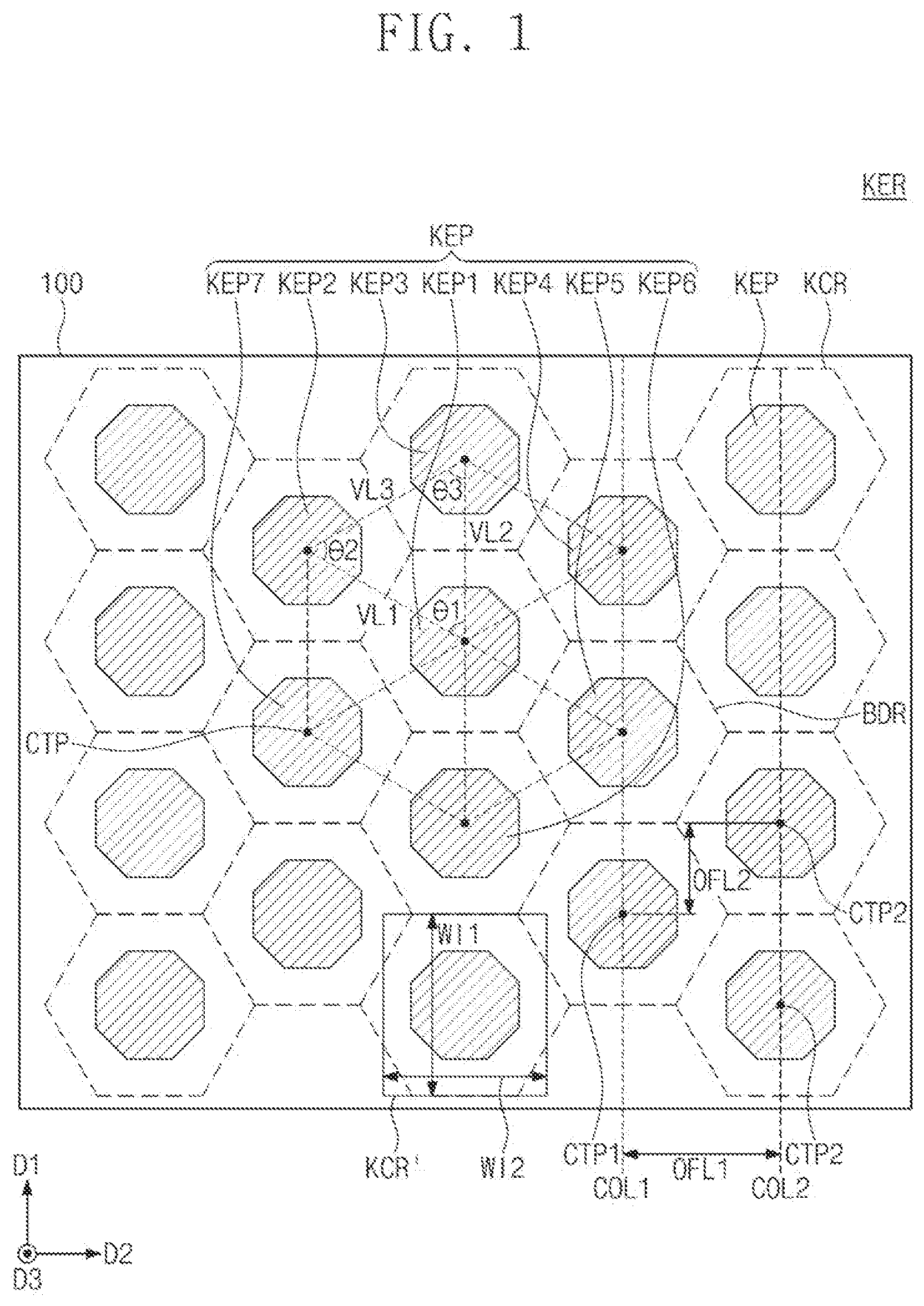
Example embodiments of the inventive concepts will now be described more fully with reference to the accompanying drawings, in which example embodiments are shown. Like numbers refer to like elements throughout. is a plan view illustrating an overlay key region according to an example embodiment of the inventive concept. Referring to , a substrate 100 including an overlay key region KER may be provided. A plurality of key patterns KEP may be disposed on the overlay key region KER. The key patterns KEP may be two-dimensionally arranged at a specific pitch. The key patterns KEP may be arranged in a honeycomb shape, under a specific rule. Each of the key patterns KEP may be provided in a unit key region KCR. The unit key region KCR may be a region enclosing the key pattern KEP. The unit key region KCR may be a unit cell of the key pattern KEP in the overlay key region KER. One key pattern KEP may be provided in one of the unit key regions KCR. The key pattern KEP may be disposed at a center of the unit key region KCR. In the present embodiment, the key pattern KEP may have an octagonal shape. However, the shape of the key pattern KEP is not limited to this example and may be variously changed (e.g., see A and 4 B ). A boundary BDR may be defined between adjacent ones of the key patterns KEP. The boundary BDR may be a border of the unit key region KCR. A planar shape of the unit key region KCR may be a hexagon. The unit key regions KCR may be disposed such that the borders BDR thereof are in contact with each other. Thus, the unit key regions KCR may be arranged in a honeycomb shape. The unit key regions KCR, which are arranged in this manner, may constitute the overlay key region KER of . In an embodiment, the key patterns KEP of may include first to seventh key patterns KEP 1 -KEP 7 . The second to seventh key patterns KEP 2 -KEP 7 may be arranged around the first key pattern KEP 1 to enclose the first key pattern KEP 1 in a clockwise direction. A center point CTP may be defined at a center of each of the first to seventh key patterns KEP 1 -KEP 7 . Six triangles may be defined by lines, which are drawn to connect the center points CTP of the first to seventh key patterns KEP 1 -KEP 7 to each other. The six triangles may constitute one hexagon. For example, the hexagon may be defined by lines connecting the center points CTP of the second to seventh key patterns KEP 2 -KEP 7 . In an embodiment, a first virtual line VL 1 may be defined to connect the center point CTP of the first key pattern KEP 1 to the center point CTP of the second key pattern KEP 2 . A second virtual line VL 2 may be defined to connect the center point CTP of the first key pattern KEP 1 to the center point CTP of the third key pattern KEP 3 . A third virtual line VL 3 may be defined to connect the center point CTP of the second key pattern KEP 2 to the center point CTP of the third key pattern KEP 3 . A length of the first virtual line VL 1 may be substantially equal to a length of the third virtual line VL 3 . The length of the first virtual line VL 1 may be equal to or different from a length of the second virtual line VL 2 . A first angle θ 1 may be defined between the first virtual line VL 1 and the second virtual line VL 2 . A second angle θ 2 may be defined between the first virtual line VL 1 and the third virtual line VL 3 . A third angle θ 3 may be defined between the second virtual line VL 2 and the third virtual line VL 3 . The first angle θ 1 may be substantially equal to the third angle θ 3 . The second angle θ 2 may be equal to or different from the first angle θ 1 . As an example, the second angle θ 2 may range from 30° to 90°. Terms such as “same,” “equal,” “planar,” or “coplanar,” as used herein when referring to orientation, layout, location, shapes, sizes, amounts, or other measures, do not necessarily mean an exactly identical orientation, layout, location, shape, size, amount, or other measure, but are intended to encompass nearly identical orientation, layout, location, shapes, sizes, amounts, or other measures within acceptable variations that may occur, for example, due to manufacturing processes. The term “substantially” may be used herein to emphasize this meaning, unless the context or other statements indicate otherwise. For example, items described as “substantially the same,” “substantially equal,” or “substantially planar,” may be exactly the same, equal, or planar, or may be the same, equal, or planar within acceptable variations that may occur, for example, due to manufacturing processes. The triangle, which is defined by the first to third virtual line VL 1 , VL 2 , and VL 3 , may be an isosceles triangle, in which the first and third virtual lines VL 1 and VL 3 have the same length. Alternatively, the triangle may be a regular or equilateral triangle. In an embodiment, the hexagonal unit key region KCR may be reduced to a rectangular unit key region KCR′ of the same area. For example, the area of the rectangular unit key region KCR′ of may be equal to the area of the hexagonal unit key region KCR. The rectangular unit key region KCR′ may have a first width WI 1 in a first direction D 1 and a second width WI 2 in a second direction D 2 . The first direction D 1 and the second direction D 2 may be perpendicular to one another. The first width WI 1 may be equal to a length in the first direction D 1 of the hexagonal unit key region KCR. The first width WI 1 may be equal to the length of the second virtual line VL 2 . For example, the first width WI 1 may be equal to a pitch between the key patterns KEP. The second width WI 2 may be smaller than the first width WI 1 . The second width WI 2 may be smaller than a length of the hexagonal unit key region KCR in the second direction D 2 . A ratio WI 2 /WI 1 of the second width WI 2 to the first width WI 1 may range from 0.7 to 0.9. An area of the overlay key region KER may be equal to a product of the number of the key patterns KEP and the area of the unit key region KCR. For example, the area of the overlay key region KER may be proportional to the area of the unit key region KCR. The smaller the area of the unit key region KCR, the smaller the area of the overlay key region KER. According to the present embodiment, for the rectangular unit key region KCR′, since the second width WI 2 is smaller than the first width WI 1 , the area of the rectangular unit key region KCR′ may be relatively decreased. Accordingly, the area of the overlay key region KER may be reduced, and this will be described in more detail with reference to A . The key patterns KEP may constitute columns, each of which includes a plurality of key patterns KEP arranged in the first direction D 1 . For example, the key patterns KEP, which are arranged in the first direction D 1 , may constitute a first column COL 1 , and the key patterns KEP, which are adjacent to the first column COL 1 in the second direction D 2 , may constitute a second column COL 2 . The first column COL 1 and the second column COL 2 may be repeatedly disposed in the second direction D 2 , and in this case, the key patterns KEP may be arranged to form the afore-described honeycomb shape. For example, one of the key patterns KEP in the first column COL 1 may have a first center point CTP 1 . A corresponding one of the key patterns KEP in the second column COL 2 , which is adjacent to the one of the key patterns KEP in the first column COL 1 , may have a second center point CTP 2 . The second column COL 2 may be offset from the first column COL 1 in the second direction D 2 by a first distance OFL 1 . In detail, the first distance OFL 1 may be a measure representing the offset between the second center point CTP 2 of the key pattern KEP of the second column COL 2 and the first center point CTP 1 of the key pattern KEP of the first column COL 1 in the second direction D 2 . The first distance OFL 1 may be equal to the second width WI 2 of the rectangular unit key region KCR′. The key patterns KEP of the second column COL 2 may be respectively offset from the key patterns KEP of the first column COL 1 in the first direction D 1 by a second distance OFL 2 . In detail, the second distance OFL 2 may be a measure representing the offset between the second center point CTP 2 of the key pattern KEP of the second column COL 2 and the first center point CTP 1 of the key pattern KEP of the first column COL 1 in the first direction D 1 . The second distance OFL 2 may be half of the first width WI 1 of the rectangular unit key region KCR′. The first distance OFL 1 may be larger than the second distance OFL 2 . The first distance OFL 1 may be larger than the second distance OFL 2 but may be smaller than two times of the second distance OFL 2 . In an embodiment, a ratio OFL 1 /OFL 2 of the first distance OFL 1 to the second distance OFL 2 may range from 1.4 to 1.8. In the present embodiment, since the ratio OFL 1 /OFL 2 ranges from 1.4 to 1.8, the arrangement shape of the key patterns KEP may be close to a regular hexagon. Accordingly, it may be possible to minimize the area of the overlay key region KER and to maximize a distance between adjacent ones of the key patterns KEP. The key patterns KEP may be placed in different layers from each other. For example, at least one of the first to seventh key patterns KEP 1 -KEP 7 may be placed in a front-end-of-line (FEOL) layer, another of the first to seventh key patterns KEP 1 -KEP 7 may be placed in a middle-of-line (MOL) layer, and other of the first to seventh key patterns KEP 1 -KEP 7 may be placed in a back-end-of-line (BEOL) layer. For example, the key patterns KEP according to the present embodiment may be arranged to be adjacent to each other and to form a honeycomb shape, when viewed in a plan view, but may be placed at vertically-different levels. is a plan view illustrating one of unit key regions of . Referring to , the unit key region KCR may include the key pattern KEP provided at a center thereof. The key pattern KEP may include a plurality of first sub-key patterns SKP 1 and a plurality of second sub-key patterns SKP 2 . For example, the first sub-key patterns SKP 1 may be bar-shaped patterns extending lengthwise in the second direction D 2 . The second sub-key patterns SKP 2 may be bar-shaped patterns extending lengthwise in the first direction D 1 . Each key pattern KEP may be composed of a combination of the first and second sub-key patterns SKP 1 and SKP 2 . A blank region BLKR may be defined around the key pattern KEP. More specifically, a blank boundary BLBD may be placed to define the blank region BLKR around the key pattern KEP. The blank boundary BLBD may be an imaginary boundary. An empty region, which does not have any pattern, may be provided between the blank boundary BLBD and the key pattern KEP. The blank boundary BLBD may have a shape corresponding to the key pattern KEP. Since the key pattern KEP according to the present embodiment has an octagonal shape, the blank boundary BLBD may also have an octagonal shape. A dummy region DMR may be provided between the blank boundary BLBD and the boundary BDR of the unit key region KCR. Dummy patterns CLP may be disposed in the dummy region DMR. For example, the dummy patterns CLP may include a cell-like pattern, which has the same shape as a cell pattern that is formed when a layer of the key pattern KEP is formed. The dummy patterns CLP may include a test element group (TEG) pattern. The dummy patterns CLP may be spaced apart from the key pattern KEP with the blank region BLKR interposed therebetween. A is a plan view illustrating an overlay key region according to a comparative example. Referring to A , the key patterns KEP may be two-dimensionally arranged on the overlay key region KER′ according to the present comparative example. The key patterns KEP according to the present comparative example may be disposed to form a checkerboard shape in the first and second directions D 1 and D 2 . As an example, the key patterns KEP may include first to fourth key patterns KEP 1 -KEP 4 . A tetragon or rectangle may be defined by lines connecting the center points CTP of the first to fourth key patterns KEP 1 -KEP 4 . For example, the key patterns KEP according to the comparative example may be arranged to form a rectangular checkerboard shape. The first virtual line VL 1 may be defined to connect the center point CTP of the first key pattern KEP 1 to the center point CTP of the second key pattern KEP 2 . The second virtual line VL 2 may be defined to connect the center point CTP of the first key pattern KEP 1 to the center point CTP of the third key pattern KEP 3 . The first virtual line VL 1 may be parallel to the second direction D 2 , and the second virtual line VL 2 may be parallel to the first direction D 1 . The first virtual line VL 1 and the second virtual line VL 2 may be orthogonal to each other. A length of the first virtual line VL 1 and a length of the second virtual line VL 2 may be substantially equal to each other. The length of the first virtual line VL 1 in the present comparative example may be equal to the length of the first virtual line VL 1 of . In the present comparative example, the key patterns KEP may be arranged at a first pitch in the first or second direction D 1 or D 2 . The first pitch between the key patterns KEP may be equal to the length of the first virtual line VL 1 or the length of the second virtual line VL 2 . A distance between the key patterns KEP according to the present comparative example may be substantially equal to the distance between the key patterns KEP in the embodiment previously described with reference to . In the present comparative example, the key pattern KEP may be provided in the rectangular unit key region KCR. The unit key region KCR may have a third width WI 3 in the first direction D 1 and a fourth width WI 4 in the second direction D 2 . The third width WI 3 may be equal to the length of the second virtual line VL 2 , and the fourth width WI 4 may be equal to the length of the first virtual line VL 1 . The third width WI 3 may be equal to the fourth width WI 4 . For example, the unit key region KCR according to the present comparative example may have a square shape. The unit key regions KCR according to the present comparative example may be disposed such that the borders BDR thereof are in contact with each other. In this case, the unit key regions KCR may be arranged to form a checkerboard shape. Referring back to A , an area of the rectangular unit key region KCR′ of may be smaller than that of the unit key region KCR of A . In detail, the first width WI 1 of the rectangular unit key region KCR′ of may be equal to the third width WI 3 of the unit key region KCR of A . However, the second width WI 2 of the rectangular unit key region KCR′ of may be smaller than the fourth width WI 4 of the unit key region KCR of A . A distance between the center points CTP of adjacent ones of the key patterns KEP of may be equal to a distance between the center points CTP of adjacent ones of the key patterns KEP′ of A . For example, a pitch or distance between adjacent one of the key patterns KEP in the embodiment of may be equal to that in the comparative example of A . However, an area of the unit key region KCR of may be smaller than an area of the unit key region KCR of A . As a result, the area of the overlay key region KER in the present embodiment may be smaller than the area of the overlay key region KER′ in the comparative example. According to an example embodiment of the inventive concept, since the key patterns KEP are arranged in a honeycomb shape, the area of the overlay key region KER may be decreased even when the distance between the key patterns KEP is unchanged. Thus, it may be possible to relatively reduce the area of the overlay key region KER and thereby to increase an integration density of the semiconductor device. B is a plan view illustrating an overlay key region according to another comparative example. Referring to B , the key patterns KEP may be two-dimensionally arranged on an overlay key region KER″ according to the present comparative example. The key patterns KEP according to the present comparative example may be disposed to form a checkerboard shape in the first and second directions D 1 and D 2 . The unit key region KCR according to the present comparative example may be defined to have the same area as the rectangular unit key region KCR′ of A . In detail, the unit key region KCR in the present comparative example may have a fifth width WI 5 in the first direction D 1 and a sixth width WI 6 in the second direction D 2 . The fifth width WI 5 may be equal to the sixth width WI 6 . A product of the fifth width WI 5 and the sixth width WI 6 may be equal to a product of the first width WI 1 and the second width WI 2 of . For example, an area of the unit key region KCR of B may be equal to the area of the rectangular unit key region KCR′ of A . In the present comparative example, the key patterns KEP may be arranged at a second pitch in the first or second direction D 1 or D 2 . The second pitch between the key patterns KEP may be the same as a distance between the center points CTP of the key patterns KEP. For example, the second pitch between the key patterns KEP may be equal to the length of the first or second virtual line VL 1 or VL 2 of B . The length of the first virtual line VL 1 of B may be smaller than the length of the first virtual line VL 1 of . The length of the second virtual line VL 2 of B may be smaller than the length of the second virtual line VL 2 of . The second pitch between the key patterns KEP may be smaller than the first pitch previously described with reference to A . The second pitch between the key patterns KEP may be smaller than the pitch between the key patterns KEP of . For example, the second pitch between the key patterns KEP may be smaller than the length of the first or second virtual line VL 1 or VL 2 of . Referring back to B , the area of the unit key region KCR of B may be equal to the area of the unit key region KCR of . That is, if the number of the key patterns KEP is unchanged, an area of the overlay key region KER″ of B may be equal to the area of the overlay key region KER of . However, a distance between adjacent ones of the key patterns KEP of B may be smaller than a distance between adjacent ones of the key patterns KEP of . Due to this small distance between the key patterns KEP, adjacent ones of the key patterns KEP in the comparative example of B may not be accurately recognized by an inspection system, and this may lead to a failure in a subsequent process. According to the embodiment shown in , it may be possible to maximize the distance between the key patterns KEP, even when the area of the overlay key region KER is unchanged. Thus, due to this increase in the distance between the key patterns KEP, the key patterns KEP may be accurately recognized by an inspection system during a semiconductor fabrication process. As a result, it may be possible to improve reliability in the semiconductor fabrication process. A and 4 B are plan views, each of which illustrates key patterns according to an example embodiment of the inventive concept. Referring to A , each of the key patterns KEP may have a tetragonal or rectangular shape. Referring to B , each of the key patterns KEP may have a hexagonal shape. According to an example embodiment of the inventive concept, the unit key region KCR may have a hexagonal shape, regardless of the shape of the key pattern KEP. The unit key region KCR may be provided to enclose the polygonal key pattern KEP placed at the center thereof. The hexagonal unit key regions KCR may be arranged such that the borders BDR thereof are in contact with each other, and thus, the key patterns KEP may be arranged to form a honeycomb shape. is a plan view illustrating a semiconductor device according to an example embodiment of the inventive concept. Referring to , the semiconductor device may include a main chip MC and a cut scribe lane CSL enclosing the main chip MC. The main chip MC may include first to fifth functional units FE 1 -FE 5 , which are integrated on the substrate 100 . The substrate 100 may be a diced portion of a semiconductor wafer. The substrate 100 may support the first to fifth functional units FE 1 -FE 5 . The main chip MC may include first to fourth boundaries CB 1 -CB 4 . The first to fourth boundaries CB 1 -CB 4 may be defined between the cut scribe lane CSL and the main chip MC. The cut scribe lane CSL may enclose the first to fourth boundaries CB 1 -CB 4 of the main chip MC. In an embodiment, the cut scribe lane CSL may include a first overlay key region KER 1 , which is provided to be adjacent to the first boundary CB 1 of the main chip MC. For example, the first overlay key region KER 1 may be left on the cut scribe lane CSL, even after a dicing process on the wafer. Each of the first to fifth functional units FE 1 -FE 5 may be a functional block constituting an integrated circuit. Each of the first to fifth functional units FE 1 -FE 5 may include one of a memory block, an analog logic block, an input/output (I/O) logic block, a central processing unit (CPU) block, and a radio frequency block. In an embodiment, the first functional unit FE 1 may include a logic cell region CER and a second overlay key region KER 2 . For example, the overlay key region may be provided not only in the scribe lane but also the functional block. The third overlay key region KER 3 may be provided in a region between the first functional unit FE 1 and the second functional unit FE 2 . Each of the first to third overlay key regions KER 1 , KER 2 , and KER 3 may be substantially the same as the overlay key region KER previously described with reference to . At least one of the first to third overlay key regions KER 1 , KER 2 , and KER 3 mentioned above may be omitted from a semiconductor device (i.e., a semiconductor chip). is a plan view illustrating a semiconductor device according to an example embodiment of the inventive concept and in particular illustrating a logic cell region and an overlay key region of . A to 7 E are sectional views illustrating lines A-A′, B-B′, C-C′, D-D′, and E-E′ of . Referring to , 6 , and 7 A to 7 E , the first functional unit FE 1 of the semiconductor chip of may include the logic cell region CER. The overlay key region KER of one of the first to third overlay key regions KER 1 , KER 2 , and KER 3 of the semiconductor chip of is exemplarily illustrated in . In an embodiment, the overlay key region KER of may be the first overlay key region KER 1 , which is provided in the cut scribe lane CSL of . In another embodiment, the overlay key region KER of may be the second overlay key region KER 2 provided in the first functional unit FE 1 of . In other embodiment, the overlay key region KER of may be the third overlay key region KER 3 , which is provided between the first and second functional units FE 1 and FE 2 of . The logic cell region CER provided on the substrate 100 may be first described in more detail. Referring to A to 7 D , the logic cell region CER may include a logic cell including a logic circuit (e.g., AND, OR, XOR, XNOR, or inverter circuit), which is configured for a specific function. For example, the logic cell of the logic cell region CER may include transistors constituting the logic device and interconnection lines connecting transistors to each other. The substrate 100 may be a semiconductor substrate that is formed of or includes silicon, germanium, silicon germanium, a compound semiconductor material, or the like. In an embodiment, the substrate 100 may be a silicon wafer. The substrate 100 may include a first active region AR 1 and a second active region AR 2 . Each of the first and second active regions AR 1 and AR 2 may be extended lengthwise in the second direction D 2 . In an embodiment, the first active region AR 1 may be an NMOSFET region, and the second active region AR 2 may be a PMOSFET region. A first active pattern AP 1 and a second active pattern AP 2 may be defined by a trench TR, which is formed in an upper portion of the substrate 100 . The first active pattern AP 1 may be provided on the first active region AR 1 , and the second active pattern AP 2 may be provided on the second active region AR 2 . The first and second active patterns AP 1 and AP 2 may be extended lengthwise in the second direction D 2 . Each of the first and second active patterns AP 1 and AP 2 may be a vertically-protruding portion of the substrate 100 . A device isolation layer ST may be provided on the substrate 100 . The device isolation layer ST may be provided to fill the trench TR. The device isolation layer ST may include a silicon oxide layer. The device isolation layer ST may not cover first and second channel patterns CH 1 and CH 2 to be described below. A first channel pattern CH 1 may be provided on the first active pattern AP 1 . A second channel pattern CH 2 may be provided on the second active pattern AP 2 . Each of the first and second channel patterns CH 1 and CH 2 may include a first semiconductor pattern SP 1 , a second semiconductor pattern SP 2 , and a third semiconductor pattern SP 3 , which are sequentially stacked. The first to third semiconductor patterns SP 1 , SP 2 , and SP 3 may be spaced apart from each other in a vertical direction (i.e., a third direction D 3 ). Each of the first to third semiconductor patterns SP 1 , SP 2 , and SP 3 may be formed of or may include at least one of silicon (Si), germanium (Ge), or silicon germanium (SiGe). For example, each of the first to third semiconductor patterns SP 1 , SP 2 , and SP 3 may be formed of or may include crystalline silicon. A plurality of first source/drain patterns SD 1 may be provided on the first active pattern AP 1 . A plurality of first recesses RS 1 may be formed in an upper portion of the first active pattern AP 1 . The first source/drain patterns SD 1 may be provided in the first recesses RS 1 , respectively. The first source/drain patterns SD 1 may be impurity regions of a first conductivity type (e.g., n-type). The first channel pattern CH 1 may be interposed between each pair of the first source/drain patterns SD 1 . For example, each pair of the first source/drain patterns SD 1 may be connected to each other by the stacked first to third semiconductor patterns SP 1 , SP 2 , and SP 3 . A plurality of second source/drain patterns SD 2 may be provided on the second active pattern AP 2 . A plurality of second recesses RS 2 may be formed in an upper portion of the second active pattern AP 2 . The second source/drain patterns SD 2 may be provided in the second recesses RS 2 , respectively. The second source/drain patterns SD 2 may be impurity regions of a second conductivity type (e.g., p-type). The second channel pattern CH 2 may be interposed between each pair of the second source/drain patterns SD 2 . For example, each pair of the second source/drain patterns SD 2 may be connected to each other by the stacked first to third semiconductor patterns SP 1 , SP 2 , and SP 3 . The first and second source/drain patterns SD 1 and SD 2 may be epitaxial patterns, which are formed by a selective epitaxial growth (SEG) process. In an embodiment, each of the first and second source/drain patterns SD 1 and SD 2 may have a top surface that is higher than a top surface of the third semiconductor pattern SP 3 . In another embodiment, a top surface of at least one of the first and second source/drain patterns SD 1 and SD 2 may be located at substantially the same level as the top surface of the third semiconductor pattern SP 3 . In an embodiment, the first source/drain patterns SD 1 may be formed of or may include the same semiconductor element (e.g., Si) as the substrate 100 . The second source/drain patterns SD 2 may include a semiconductor material (e.g., SiGe) whose lattice constant is greater than that of the substrate 100 . In this case, the pair of the second source/drain patterns SD 2 may exert a compressive stress on the second channel pattern CH 2 therebetween. A side surface of each of the first and second source/drain patterns SD 1 and SD 2 may have an uneven or embossing shape. For example, the side surface of each of the first and second source/drain patterns SD 1 and SD 2 may have a wavy profile. The side surface of each of the first and second source/drain patterns SD 1 and SD 2 may protrude toward first to third portions PO 1 , PO 2 , and PO 3 of a gate electrode GE, which will be described below. Gate electrodes GE may be provided to cross the first and second channel patterns CH 1 and CH 2 and to extend lengthwise in the first direction D 1 . The gate electrodes GE may be arranged at a first pitch in the second direction D 2 . Each of the gate electrodes GE may be vertically overlapped with the first and second channel patterns CH 1 and CH 2 . The gate electrode GE may include a first portion PO 1 interposed between the active pattern AP 1 or AP 2 and the first semiconductor pattern SP 1 , a second portion PO 2 interposed between the first semiconductor pattern SP 1 and the second semiconductor pattern SP 2 , a third portion PO 3 interposed between the second semiconductor pattern SP 2 and the third semiconductor pattern SP 3 , and a fourth portion PO 4 on the third semiconductor pattern SP 3 . Referring to D , the gate electrode GE may be provided on a top surface TS, a bottom surface BS, and opposite side surfaces SW of each of the first to third semiconductor patterns SP 1 , SP 2 , and SP 3 . That is, the transistor according to the present embodiment may be a three-dimensional field effect transistor (e.g., MBCFET or GAAFET) in which the gate electrode GE is provided to three-dimensionally surround the channel pattern. Referring back to A to 7 D , a pair of gate spacers GS may be respectively disposed on opposite side surfaces of the fourth portion PO 4 of the gate electrode GE. The gate spacers GS may be extended along the gate electrode GE and in the first direction D 1 . Top surfaces of the gate spacers GS may be higher than a top surface of the gate electrode GE. The top surfaces of the gate spacers GS may be coplanar with a top surface of a first interlayer insulating layer 110 , which will be described below. In an embodiment, the gate spacers GS may be formed of or may include at least one of SiCN, SiCON, or SiN. In another embodiment, the gate spacers GS may be a multi-layered structure, which is formed of or includes at least two different materials selected from SiCN, SiCON, and SiN. A gate capping pattern GP may be provided on the gate electrode GE. The gate capping pattern GP may be extended lengthwise along the gate electrode GE or in the first direction D 1 . The gate capping pattern GP may be formed of or may include a material having an etch selectivity with respect to first and second interlayer insulating layers 110 and 120 , which will be described below. In detail, the gate capping pattern GP may be formed of or may include at least one of SiON, SiCN, SiCON, or SiN. A gate insulating layer GI may be interposed between the gate electrode GE and the first channel pattern CH 1 and between the gate electrode GE and the second channel pattern CH 2 . The gate insulating layer GI may cover the top surface TS, the bottom surface BS, and the opposite side surfaces SW of each of the first to third semiconductor patterns SP 1 , SP 2 , and SP 3 . The gate insulating layer GI may cover a top surface of the device isolation layer ST below the gate electrode GE. In an embodiment, referring to A and 7 B , the gate insulating layer GI may include an interface layer IL and a high-k dielectric layer HK. The interface layer IL may include a silicon oxide layer or a silicon oxynitride layer. The high-k dielectric layer HK may be formed of or may include a high-k dielectric material whose dielectric constant is higher than silicon oxide. As an example, the high-k dielectric layer HK may be formed of or may include at least one of, for example, hafnium oxide, hafnium silicon oxide, hafnium zirconium oxide, hafnium tantalum oxide, lanthanum oxide, zirconium oxide, zirconium silicon oxide, tantalum oxide, titanium oxide, barium strontium titanium oxide, barium titanium oxide, strontium titanium oxide, lithium oxide, aluminum oxide, lead scandium tantalum oxide, or lead zinc niobate. Referring back to A to 7 D , the gate electrode GE may include a first metal pattern and a second metal pattern on the first metal pattern. The first metal pattern may be provided on the gate insulating layer GI and may be adjacent to the first to third semiconductor patterns SP 1 , SP 2 , and SP 3 . The first metal pattern may include a work-function metal, which can be used to adjust a threshold voltage of the transistor. By adjusting a thickness and composition of the first metal pattern, it may be possible to realize a transistor having a desired threshold voltage. For example, the first to third portions PO 1 , PO 2 , and PO 3 of the gate electrode GE may be composed of the first metal pattern or the work-function metal. The first metal pattern may include a metal nitride layer. For example, the first metal pattern may include a layer that is composed of at least one metallic material, which is selected from the group consisting of titanium (Ti), tantalum (Ta), aluminum (Al), tungsten (W) and molybdenum (Mo), and nitrogen (N). In an embodiment, the first metal pattern may further include carbon (C). The first metal pattern may include a plurality of work function metal layers which are stacked. The second metal pattern may be formed of or may include a metallic material whose resistance is lower than the first metal pattern. For example, the second metal pattern may be formed of or may include at least one metallic material, which is selected from the group consisting of tungsten (W), aluminum (Al), titanium (Ti), and tantalum (Ta). The fourth portion PO 4 of the gate electrode GE may include the first metal pattern and the second metal pattern on the first metal pattern. A first interlayer insulating layer 110 may be provided on the substrate 100 . The first interlayer insulating layer 110 may cover the gate spacers GS and the first and second source/drain patterns SD 1 and SD 2 . The first interlayer insulating layer 110 may have a top surface that is substantially coplanar with the top surface of the gate capping pattern GP and the top surface of the gate spacer GS. A second interlayer insulating layer 120 may be formed on the first interlayer insulating layer 110 to cover the gate capping pattern GP. A third interlayer insulating layer 130 may be provided on the second interlayer insulating layer 120 . A fourth interlayer insulating layer 140 may be provided on the third interlayer insulating layer 130 . In an embodiment, at least one of the first to fourth interlayer insulating layers 110 to 140 may include a silicon oxide layer. The logic cell region CER may have a first boundary BD 1 and a second boundary BD 2 , which are opposite to each other in the second direction D 2 . The first and second boundaries BD 1 and BD 2 may be extended lengthwise in the first direction D 1 . The logic cell region CER may have a third boundary BD 3 and a fourth boundary BD 4 , which are opposite to each other in the first direction D 1 . The third and fourth boundaries BD 3 and BD 4 may be extended lengthwise in the second direction D 2 . A pair of division structures DB, which are opposite to each other in the second direction D 2 , may be provided at both sides of the logic cell region CER. For example, the pair of the division structures DB may be respectively provided on the first and second borders BD 1 and BD 2 of the single height cell SHC. The division structure DB may be extended in the first direction D 1 to be parallel to the gate electrodes GE. A pitch between the division structure DB and the gate electrode GE adjacent thereto may be equal to the first pitch. The division structure DB may be provided to penetrate the first and second interlayer insulating layers 110 and 120 and may be extended into the first and second active patterns AP 1 and AP 2 . The division structure DB may be provided to penetrate an upper portion of each of the first and second active patterns AP 1 and AP 2 . The division structure DB may electrically separate an active region of each of the single height cell SHC from an active region of a neighboring cell. For example, lower surfaces of the division structures DB may be lower than an upper surface of the substrate 100 . Active contacts AC may be provided to penetrate the first and second interlayer insulating layers 110 and 120 and to be electrically connected to the first and second source/drain patterns SD 1 and SD 2 , respectively. A pair of the active contacts AC may be respectively provided at both sides of the gate electrode GE. When viewed in a plan view, the active contact AC may be a bar-shaped pattern that is extended lengthwise in the first direction D 1 . The active contact AC may be a self-aligned contact. For example, the active contact AC may be formed by a self-alignment process using the gate capping pattern GP and the gate spacer GS. For example, the active contact AC may cover at least a portion of the side surface of the gate spacer GS. Although not shown, the active contact AC may cover a portion of the top surface of the gate capping pattern GP. Metal-semiconductor compound layers SC (e.g., silicide layers) may be respectively interposed between the active contact AC and the first source/drain pattern SD 1 and between the active contact AC and the second source/drain pattern SD 2 . The active contact AC may be electrically connected to the source/drain pattern SD 1 or SD 2 through the metal-semiconductor compound layer SC. For example, the metal-semiconductor compound layer SC may be formed of or may include at least one of titanium silicide, tantalum silicide, tungsten silicide, nickel silicide, or cobalt silicide. Gate contacts GC may be provided to penetrate the second interlayer insulating layer 120 and the gate capping pattern GP and to be electrically connected to the gate electrodes GE, respectively. When viewed in a plan view, the gate contacts GC may be disposed to be respectively overlapped with the first and second active regions AR 1 and AR 2 . As an example, the gate contact GC may be provided on the second active pattern AP 2 (e.g., see B ). In an embodiment, referring to B , an upper portion of the active contact AC adjacent to the gate contact GC may be filled with an upper insulating pattern UIP. A bottom surface of the upper insulating pattern UIP may be lower than a bottom surface of the gate contact GC. For example, a top surface of the active contact AC adjacent to the gate contact GC may be formed at a level, which is lower than the bottom surface of the gate contact GC, by the upper insulating pattern UIP. Accordingly, it may be possible to prevent the gate contact GC and the active contact AC, which are adjacent to each other, from being in contact with each other and thereby to prevent a short circuit issue from occurring therebetween. Each of the active and gate contacts AC and GC may include a conductive pattern FM and a barrier pattern BM enclosing the conductive pattern FM. For example, the conductive pattern FM may be formed of or may include at least one of metallic materials (e.g., aluminum, copper, tungsten, molybdenum, and cobalt). The barrier pattern BM may cover side and bottom surfaces of the conductive pattern FM. In an embodiment, the barrier pattern BM may include a metal layer and a metal nitride layer. The metal layer may be formed of or may include at least one of titanium, tantalum, tungsten, nickel, cobalt, or platinum. The metal nitride layer may be formed of or may include at least one of titanium nitride (TiN), tantalum nitride (TaN), tungsten nitride (WN), nickel nitride (NiN), cobalt nitride (CoN), or platinum nitride (PtN). A first metal layer M 1 may be provided in the third interlayer insulating layer 130 . For example, the first metal layer M 1 may include a first power line M 1 _R 1 , a second power line M 1 _R 2 , and first interconnection lines M 1 _I. Each of the interconnection lines M 1 _R 1 , M 1 _R 2 , and M 1 _I of the first metal layer M 1 may be extended lengthwise in the second direction D 2 and in parallel to each other. In detail, the first and second power lines M 1 _R 1 and M 1 _R 2 may be provided on the third and fourth boundaries BD 3 and BD 4 , respectively, of the logic cell region CER. The first power line M 1 _R 1 may be extended lengthwise along the third border BD 3 and in the second direction D 2 . The second power line M 1 _R 2 may be extended lengthwise along the fourth border BD 4 and in the second direction D 2 . The first power line M 1 _R 1 may be a path for providing a drain voltage VDD, for example, a power voltage. The second power line M 1 _R 2 may be a path for providing a source voltage VSS, for example, a ground voltage. The first interconnection lines M 1 _I of the first metal layer M 1 may be disposed between the first and second power lines M 1 _R 1 and M 1 _R 2 . The first interconnection lines M 1 _I of the first metal layer M 1 may be arranged at a second pitch in the first direction D 1 . The second pitch may be smaller than the first pitch. A linewidth of each of the first interconnection lines M 1 _I may be smaller than a linewidth of each of the first and second power lines M 1 _R 1 and M 1 _R 2 . The first metal layer M 1 may further include first vias VI 1 . The first vias VI 1 may be respectively disposed below the interconnection lines M 1 _R 1 , M 1 _R 2 , and M 1 _I of the first metal layer M 1 . The active contact AC and the interconnection line of the first metal layer M 1 may be electrically connected to each other through the first via VI 1 . The gate contact GC and the interconnection line of the first metal layer M 1 may be electrically connected to each other through the first via VI 1 . The interconnection line of the first metal layer M 1 and the first via VI 1 thereunder may be formed by separate processes. For example, the interconnection line and the first via VI 1 of the first metal layer M 1 may be independently formed by respective single damascene processes. The semiconductor device according to the present embodiment may be fabricated using a sub-20 nm process. A second metal layer M 2 may be provided in the fourth interlayer insulating layer 140 . The second metal layer M 2 may include a plurality of second interconnection lines M 2 _I. Each of the second interconnection lines M 2 _I of the second metal layer M 2 may be a line- or bar-shaped pattern that is extended lengthwise in the first direction D 1 . For example, the second interconnection lines M 2 _I may be extended lengthwise in the first direction D 1 and in parallel to each other. The second metal layer M 2 may further include second vias VI 2 , which are respectively provided below the second interconnection lines M 2 _I. The interconnection lines of the first and second metal layers M 1 and M 2 may be electrically connected to each other through the second via VI 2 . The interconnection line of the second metal layer M 2 and the second via VI 2 thereunder may be formed together by a dual damascene process. The interconnection lines of the first metal layer M 1 may be formed of or may include a conductive material that is the same as or different from those of the second metal layer M 2 . For example, the interconnection lines of the first and second metal layers M 1 and M 2 may be formed of or may include at least one of metallic materials (e.g., aluminum, copper, tungsten, ruthenium, molybdenum, and cobalt). Although not shown, a plurality of metal layers (e.g., M 3 , M 4 , M 5 , and so forth) may be additionally stacked on the fourth interlayer insulating layer 140 . Each of the stacked metal layers may include interconnection lines, which are used as routing paths between cells. The overlay key region KER will be described in more detail with reference to E . The overlay key region KER may include a plurality of the key patterns KEP, which are arranged in a honeycomb shape. The arrangement or disposition of the key patterns KEP may be substantially the same as that in the embodiment described with reference to . Each of the key patterns KEP may be disposed in the unit key region KCR. The unit key region KCR may include the first and second sub-key patterns SKP 1 and SKP 2 , the blank region BLKR, and the dummy region DMR including the dummy patterns CLP, as previously described with reference to . The key patterns KEP of may include the first to seventh key patterns KEP 1 -KEP 7 . The first to seventh key patterns KEP 1 -KEP 7 may be disposed in the same layer or in at least two different layers. For example, referring to E , the seventh key pattern KEP 7 may include the first and second sub-key patterns SKP 1 and SKP 2 , which are provided in the first metal layer M 1 . The fifth key pattern KEP 5 may include the first and second sub-key patterns SKP 1 and SKP 2 , which are provided in the second metal layer M 2 . For example, the seventh key pattern KEP 7 and the fifth key pattern KEP 5 may be located at different levels. In an embodiment, the seventh key pattern KEP 7 , which is formed in the first metal layer M 1 , may serve as an overlay key, which is used to align a photomask in a photolithography process to form the second metal layer M 2 . The fifth key pattern KEP 5 , which is formed in the second metal layer M 2 , may be used as an overlay key in a photolithography process for forming a third metal layer. According to an example embodiment of the inventive concept, key patterns may be arranged in a honeycomb shape, and this may make it possible to minimize an area of an overlay key region and thereby to increase an integration density of a semiconductor device. Due to the honeycomb shape, it may be possible to secure a sufficient distance between adjacent ones of the key patterns, even when the area of the overlay key region is reduced. Accordingly, it may be possible to increase accuracy in a process of inspecting the key patterns and thereby to improve reliability in a semiconductor fabrication process. While example embodiments of the inventive concept have been particularly shown and described, it will be understood by one of ordinary skill in the art that variations in form and detail may be made therein without departing from the spirit and scope of the attached claims.
Figures (13)
Citations
This patent cites (11)
- US7463367
- US7755207
- US7855436
- US8339595
- US2007/0069398
- US2009/0001521
- US2009/0224413
- US2010050148
- US1020040107299
- US100896850
- US1020100009835