Display Device and Manufacturing Method Thereof
Abstract
According to one embodiment, a display device includes a lower electrode, a rib including a pixel aperture, a partition including a lower portion on the rib and an upper portion protruding from a side surface of the lower portion, an upper electrode facing the lower electrode, an organic layer between the electrodes, and a sealing layer covering a display element and the partition. The rib includes a first rib layer and a second rib layer which covers the first rib layer. The sealing layer and the first rib layer are formed of a first inorganic material. The second rib layer is formed of a second inorganic material different from the first inorganic material.
Claims (20)
1 . A display device comprising: a lower electrode; a rib comprising a pixel aperture which overlaps the lower electrode; a partition comprising a lower portion provided on the rib and an upper portion which protrudes from a side surface of the lower portion; an upper electrode which faces the lower electrode; an organic layer which is located between the lower electrode and the upper electrode, is in contact with the lower electrode through the pixel aperture, and emits light based on a potential difference between the lower electrode and the upper electrode; and a sealing layer which continuously covers a display element including the lower electrode, the upper electrode and the organic layer and the partition, wherein the rib includes a first rib layer and a second rib layer which covers the first rib layer, the sealing layer and the first rib layer are formed of a first inorganic material, the second rib layer is formed of a second inorganic material different from the first inorganic material, and the second inorganic material is silicon oxynitride.
8 . A manufacturing method of a display device, including: forming a lower electrode; forming a first rib layer which covers the lower electrode by a first inorganic material; forming a second rib layer which covers the first rib layer by a second inorganic material different from the first inorganic material; forming a rib comprising a pixel aperture which overlaps the lower electrode by patterning the first rib layer and the second rib layer; forming a partition comprising a lower portion provided on the rib and an upper portion which protrudes from a side surface of the lower portion; forming an organic layer which is in contact with the lower electrode through the pixel aperture; forming an upper electrode which covers the organic layer; and forming a sealing layer which covers a display element including the lower electrode, the upper electrode and the organic layer by the first inorganic material, wherein the second inorganic material is silicon oxynitride.
17 . A display device comprising: a lower electrode; a rib comprising a pixel aperture which overlaps the lower electrode; a partition comprising a lower portion provided on the rib and an upper portion which protrudes from a side surface of the lower portion; an upper electrode which faces the lower electrode; an organic layer which is located between the lower electrode and the upper electrode, is in contact with the lower electrode through the pixel aperture, and emits light based on a potential difference between the lower electrode and the upper electrode; and a sealing layer which continuously covers a display element including the lower electrode, the upper electrode and the organic layer and the partition, wherein the rib includes a first rib layer and a second rib layer which covers the first rib layer, the sealing layer and the first rib layer are formed of a first inorganic insulating material, and the second rib layer is formed of a second inorganic insulating material different from the first inorganic insulating material.
Show 17 dependent claims
2 . The display device of claim 1 , wherein the first inorganic material is silicon nitride.
3 . The display device of claim 1 , wherein a thickness of the rib is less than a height of the partition.
4 . The display device of claim 1 , wherein a thickness of the rib is greater than or equal to 1.5 times a thickness of the lower electrode and less than or equal to 5 times the thickness of the lower electrode.
5 . The display device of claim 1 , wherein a thickness of the rib is greater than or equal to 200 nm and less than or equal to 600 nm.
6 . The display device of claim 5 , wherein a thickness of the second rib layer is greater than or equal to 50 nm and less than or equal to 100 nm.
7 . The display device of claim 1 , wherein the display element further comprises a cap layer which covers the upper electrode.
9 . The manufacturing method of claim 8 , wherein the first inorganic material is silicon nitride.
10 . The manufacturing method of claim 8 , further including: forming a resist on the sealing layer; and removing a part of the sealing layer located above the partition by a dry etching using the resist as a mask.
11 . The manufacturing method of claim 10 , further including removing a part of the organic layer and a part of the upper electrode by an etching using the resist as a mask.
12 . The manufacturing method of claim 8 , wherein a thickness of the rib is less than a height of the partition.
13 . The manufacturing method of claim 8 , wherein a thickness of the rib is greater than or equal to 1.5 times a thickness of the lower electrode and less than or equal to 5 times the thickness of the lower electrode.
14 . The manufacturing method of claim 8 , wherein a thickness of the rib is greater than or equal to 200 nm and less than or equal to 600 nm.
15 . The manufacturing method of claim 8 , wherein a thickness of the second rib layer is greater than or equal to 50 nm and less than or equal to 100 nm.
16 . The manufacturing method of claim 8 , further including forming a cap layer which covers the upper electrode before forming the sealing layer.
18 . The display device of claim 17 , wherein the first rib layer includes a lower surface in direct contact with the lower electrode, an upper surface opposing the lower surface, and a side surface connecting the lower surface to the upper surface, and the second rib layer includes a lower surface in direct contact with the upper surface of the first rib layer and covering an entirety of the upper surface of the first rib layer, and an upper surface opposing the lower surface of the second rib layer and in direct contact with the lower portion of the partition.
19 . The display device of claim 18 , wherein the lower portion of the partition includes a first metal layer formed of a first metal material, and a second metal layer disposed on the first metal layer and formed of a second metal material, and a thickness of the second metal layer is greater than a thickness of the first metal layer.
20 . The display device of claim 19 , wherein the first metal material is different from the second metal material.
Full Description
Show full text →
CROSS-REFERENCE TO RELATED APPLICATIONS
This application is based upon and claims the benefit of priority from Japanese Patent Application No. 2022-096622, filed Jun. 15, 2022, the entire contents of which are incorporated herein by reference. FIELD Embodiments described herein relate generally to a display device and a manufacturing method thereof.
BACKGROUND
Recently, display devices to which an organic light emitting diode (OLED) is applied as a display element have been put into practical use. This display element comprises a lower electrode, an organic layer which covers the lower electrode, and an upper electrode which covers the organic layer. When such a display device is manufactured, a technique which improves reliability is required.
BRIEF DESCRIPTION OF THE DRAWINGS
is a diagram showing a configuration example of a display device according to an embodiment. is a diagram showing an example of the layout of subpixels. is a schematic cross-sectional view of the display device along the III-III line of . is a schematic cross-sectional view showing the structure of a partition located between a first subpixel and a second subpixel and its vicinity. is a flowchart showing an example of the manufacturing method of the display device according to the embodiment. is a schematic cross-sectional view showing part of the manufacturing process of the display device according to the embodiment. is a schematic cross-sectional view showing a manufacturing process following . is a schematic cross-sectional view showing a manufacturing process following . is a schematic cross-sectional view showing a manufacturing process following . is a schematic cross-sectional view showing a manufacturing process following . is a schematic cross-sectional view showing a manufacturing process following . is a schematic cross-sectional view showing a manufacturing process following . is a schematic cross-sectional view showing a manufacturing process following . is a schematic cross-sectional view showing a manufacturing process following . is a schematic cross-sectional view showing a manufacturing process following . is a schematic cross-sectional view showing a manufacturing process following . is a schematic cross-sectional view showing a manufacturing process following . is a schematic cross-sectional view showing a manufacturing process following . is a schematic cross-sectional view showing a manufacturing process following . is a schematic cross-sectional view showing a manufacturing process following .
DETAILED DESCRIPTION
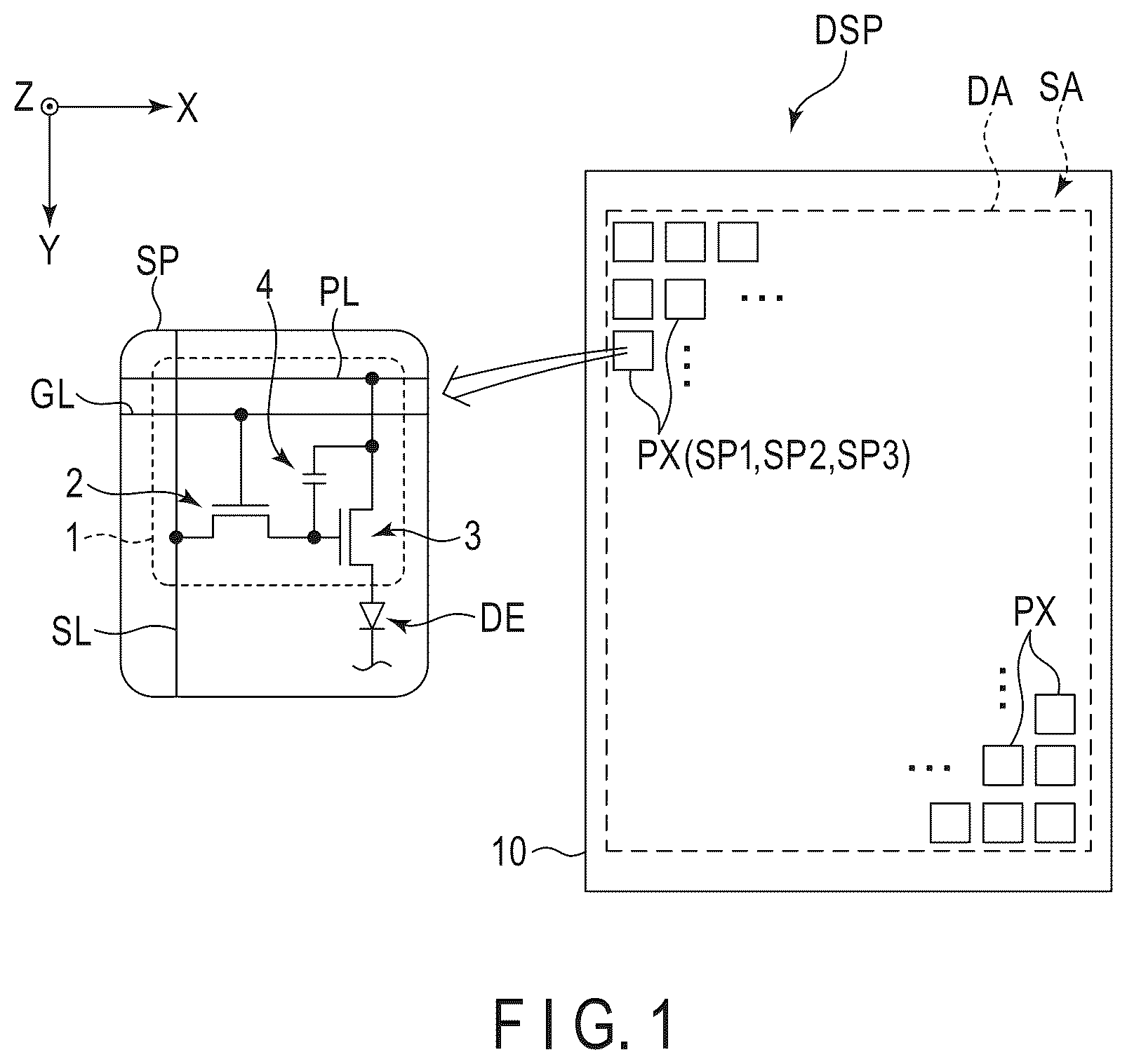
In general, according to one embodiment, a display device comprises a lower electrode, a rib comprising a pixel aperture which overlaps the lower electrode, a partition comprising a lower portion provided on the rib and an upper portion which protrudes from a side surface of the lower portion, an upper electrode which faces the lower electrode, an organic layer which is located between the lower electrode and the upper electrode, is in contact with the lower electrode through the pixel aperture, and emits light based on a potential difference between the lower electrode and the upper electrode, and a sealing layer which continuously covers a display element including the lower electrode, the upper electrode and the organic layer and the partition. The rib includes a first rib layer and a second rib layer which covers the first rib layer. The sealing layer and the first rib layer are formed of a first inorganic material. The second rib layer is formed of a second inorganic material different from the first inorganic material. According to another embodiment, a manufacturing method of a display device includes forming a lower electrode, forming a first rib layer which covers the lower electrode by a first inorganic material, forming a second rib layer which covers the first rib layer by a second inorganic material different from the first inorganic material, forming a rib comprising a pixel aperture which overlaps the lower electrode by patterning the first rib layer and the second rib layer, forming a partition comprising a lower portion provided on the rib and an upper portion which protrudes from a side surface of the lower portion, forming an organic layer which is in contact with the lower electrode through the pixel aperture, forming an upper electrode which covers the organic layer, and forming a sealing layer which covers a display element including the lower electrode, the upper electrode and the organic layer by the first inorganic material. The embodiments can improve the reliability of a display device. Embodiments will be described with reference to the accompanying drawings. The disclosure is merely an example, and proper changes in keeping with the spirit of the invention, which are easily conceivable by a person of ordinary skill in the art, come within the scope of the invention as a matter of course. In addition, in some cases, in order to make the description clearer, the widths, thicknesses, shapes, etc., of the respective parts are illustrated schematically in the drawings, rather than as an accurate representation of what is implemented. However, such schematic illustration is merely exemplary, and in no way restricts the interpretation of the invention. In addition, in the specification and drawings, structural elements which function in the same or a similar manner to those described in connection with preceding drawings are denoted by like reference numbers, detailed description thereof being omitted unless necessary. In the drawings, in order to facilitate understanding, an X-axis, a Y-axis and a Z-axis orthogonal to each other are shown depending on the need. A direction parallel to the X-axis is referred to as a first direction X. A direction parallel to the Y-axis is referred to as a second direction Y. A direction parallel to the Z-axis is referred to as a third direction Z. When various elements are viewed parallel to the third direction Z, the appearance is defined as a plan view. The display device of the present embodiment is an organic electroluminescent display device comprising an organic light emitting diode (OLED) as a display element, and could be mounted on a television, a personal computer, a vehicle-mounted device, a tablet, a smartphone, a mobile phone, etc. is a diagram showing a configuration example of a display device DSP according to an embodiment. The display device DSP comprises a display area DA which displays an image and a surrounding area SA around the display area DA on an insulating substrate 10 . The substrate 10 may be glass or a resinous film having flexibility. In the present embodiment, the substrate 10 is rectangular as seen in plan view. It should be noted that the shape of the substrate 10 in plan view is not limited to a rectangular shape and may be another shape such as a square shape, a circular shape or an elliptic shape. The display area DA comprises a plurality of pixels PX arrayed in matrix in a first direction X and a second direction Y. Each pixel PX includes a plurality of subpixels SP. For example, each pixel PX includes a blue first subpixel SP 1 , a green second subpixel SP 2 and a red third subpixel SP 3 . Each pixel PX may include a subpixel SP which exhibits another color such as white in addition to subpixels SP 1 , SP 2 and SP 3 or instead of one of subpixels SP 1 , SP 2 and SP 3 . Each subpixel SP comprises a pixel circuit 1 and a display element DE driven by the pixel circuit 1 . The pixel circuit 1 comprises a pixel switch 2 , a drive transistor 3 and a capacitor 4 . The pixel switch 2 and the drive transistor 3 are, for example, switching elements consisting of thin-film transistors. The gate electrode of the pixel switch 2 is connected to a scanning line GL. One of the source electrode and drain electrode of the pixel switch 2 is connected to a signal line SL. The other one is connected to the gate electrode of the drive transistor 3 and the capacitor 4 . In the drive transistor 3 , one of the source electrode and the drain electrode is connected to a power line PL and the capacitor 4 , and the other one is connected to the display element DE. The display element DE is an organic light emitting diode (OLED) as a light emitting element. It should be noted that the configuration of the pixel circuit 1 is not limited to the example shown in the figure. For example, the pixel circuit 1 may comprise more thin-film transistors and capacitors. is a diagram showing an example of the layout of subpixels SP 1 , SP 2 and SP 3 . In the example of , the first subpixel SP 1 and the third subpixel SP 3 are arranged in the first direction X. The first subpixel SP 1 and the second subpixel SP 2 are also arranged in the first direction X. Further, the second subpixel SP 2 and the third subpixel SP 3 are arranged in the second direction Y. When subpixels SP 1 , SP 2 and SP 3 are provided in line with this layout, in the display area DA, a column in which subpixels SP 2 and SP 3 are alternately provided in the second direction Y and a column in which a plurality of first subpixels SP 1 are repeatedly provided in the second direction Y are formed. These columns are alternately arranged in the first direction X. It should be noted that the layout of subpixels SP 1 , SP 2 and SP 3 is not limited to the example of . As another example, subpixels SP 1 , SP 2 and SP 3 in each pixel PX may be arranged in order in the first direction X. A rib 5 and a partition 6 are provided in the display area DA. The rib 5 comprises a first pixel aperture AP 1 in the first subpixel SP 1 , comprises a second pixel aperture AP 2 in the second subpixel SP 2 and comprises a third pixel aperture AP 3 in the third subpixel SP 3 . In the example of , the area of the first pixel aperture AP 1 is greater than that of the second pixel aperture AP 2 . The area of the first pixel aperture AP 1 is greater than that of the third pixel aperture AP 3 . Further, the area of the third pixel aperture AP 3 is less than that of the second pixel aperture AP 2 . The partition 6 is provided in the boundary between adjacent subpixels SP and overlaps the rib 5 as seen in plan view. The partition 6 comprises a plurality of first partitions 6 x extending in the first direction X and a plurality of second partitions 6 y extending in the second direction Y. The first partitions 6 x are provided between the pixel apertures AP 2 and AP 3 which are adjacent to each other in the second direction Y and between two first pixel apertures AP 1 which are adjacent to each other in the second direction Y. Each second partition 6 y is provided between the pixel apertures AP 1 and AP 2 which are adjacent to each other in the first direction X and between the pixel apertures AP 1 and AP 3 which are adjacent to each other in the first direction X. In the example of , the first partitions 6 x and the second partitions 6 y are connected to each other. In this configuration, the partition 6 has a grating shape surrounding the pixel apertures AP 1 , AP 2 and AP 3 as a whole. In other words, the partition 6 comprises apertures in subpixels SP 1 , SP 2 and SP 3 in a manner similar to that of the rib 5 . The first subpixel SP 1 comprises a first lower electrode LE 1 , a first upper electrode UE 1 and a first organic layer OR 1 overlapping the first pixel aperture AP 1 . The second subpixel SP 2 comprises a second lower electrode LE 2 , a second upper electrode UE 2 and a second organic layer OR 2 overlapping the second pixel aperture AP 2 . The third subpixel SP 3 comprises a third lower electrode LE 3 , a third upper electrode UE 3 and a third organic layer OR 3 overlapping the third pixel aperture AP 3 . The first lower electrode LE 1 , the first upper electrode UE 1 and the first organic layer OR 1 constitute the first display element DE 1 of the first subpixel SP 1 . The second lower electrode LE 2 , the second upper electrode UE 2 and the second organic layer OR 2 constitute the second display element DE 2 of the second subpixel SP 2 . The third lower electrode LE 3 , the third upper electrode UE 3 and the third organic layer OR 3 constitute the third display element DE 3 of the third subpixel SP 3 . Each of the display elements DE 1 , DE 2 and DE 3 may include a cap layer (optical adjustment layer) as described later. The first lower electrode LE 1 is connected to the pixel circuit 1 (see ) of the first subpixel SP 1 through a first contact hole CH 1 . The second lower electrode LE 2 is connected to the pixel circuit 1 of the second subpixel SP 2 through a second contact hole CH 2 . The third lower electrode LE 3 is connected to the pixel circuit 1 of the third subpixel SP 3 through a third contact hole CH 3 . In the example of , the contact holes CH 2 and CH 3 entirely overlap the first partition 6 X between the pixel apertures AP 2 and AP 3 which are adjacent to each other in the second direction Y. The first contact hole CH 1 entirely overlaps the first partition 6 x between two first pixel apertures AP 1 which are adjacent to each other in the second direction Y. As another example, at least part of the contact hole CH 1 , CH 2 or CH 3 may not overlap the first partition 6 x. is a schematic cross-sectional view of the display device DSP along the III-III line of . A circuit layer 11 is provided on the substrate 10 described above. The circuit layer 11 includes various circuits and lines such as the pixel circuit 1 , scanning line GL, signal line SL and power line PL shown in . The circuit layer 11 is covered with an organic insulating layer 12 . The organic insulating layer 12 functions as a planarization film which planarizes the irregularities formed by the circuit layer 11 . Although not shown in the section of , all of the contact holes CH 1 , CH 2 and CH 3 described above are provided in the organic insulating layer 12 . The lower electrodes LE 1 , LE 2 and LE 3 are provided on the organic insulating layer 12 . The rib 5 is provided on the organic insulating layer 12 and the lower electrodes LE 1 , LE 2 and LE 3 . The end portions of the lower electrodes LE 1 , LE 2 and LE 3 are covered with the rib 5 . The partition 6 includes a conductive lower portion 61 provided on the rib 5 and an upper portion 62 provided on the lower portion 61 . The upper portion 62 has a width greater than that of the lower portion 61 . By this configuration, in , the both end portions of the upper portion 62 protrude relative to the side surfaces of the lower portion 61 . This shape of the partition 6 may be called an overhang shape. The first organic layer OR 1 covers the first lower electrode LE 1 through the first pixel aperture AP 1 . The first upper electrode UE 1 covers the first organic layer OR 1 and faces the first lower electrode LE 1 . The second organic layer OR 2 covers the second lower electrode LE 2 through the second pixel aperture AP 2 . The second upper electrode UE 2 covers the second organic layer OR 2 and faces the second lower electrode LE 2 . The third organic layer OR 3 covers the third lower electrode LE 3 through the third pixel aperture AP 3 . The third upper electrode UE 3 covers the third organic layer OR 3 and faces the third lower electrode LE 3 . In the example of , a first cap layer CP 1 is provided on the first upper electrode UE 1 . A second cap layer CP 2 is provided on the second upper electrode UE 2 . A third cap layer CP 3 is provided on the third upper electrode UE 3 . The cap layers CP 1 , CP 2 and CP 3 adjust the optical property of the light emitted from the organic layers OR 1 , OR 2 and OR 3 , respectively. A first sealing layer SE 1 is provided in the first subpixel SP 1 . A second sealing layer SE 2 is provided in the second subpixel SP 2 . A third sealing layer SE 3 is provided in the third subpixel SP 3 . The first sealing layer SE 1 continuously covers the first cap layer CP 1 and the partition 6 around the first subpixel SP 1 . The second sealing layer SE 2 continuously covers the second cap layer CP 2 and the partition 6 around the second subpixel SP 2 . The third sealing layer SE 3 continuously covers the third cap layer CP 3 and the partition 6 around the third subpixel SP 3 . The end portions (peripheral portions) of the sealing layers SE 1 , SE 2 and SE 3 are located above the upper portions 62 . In the example of , the end portions of the sealing layers SE 1 and SE 2 located above the upper portion 62 of the partition 6 between subpixels SP 1 and SP 2 are spaced apart from each other. The end portions of the sealing layers SE 1 and SE 3 located above the upper portion 62 of the partition 6 between subpixels SP 1 and SP 3 are spaced apart from each other. The sealing layers SE 1 , SE 2 and SE 3 are covered with a resin layer 13 . The resin layer 13 is covered with a sealing layer 14 . Further, the sealing layer 14 is covered with a resin layer 15 . Each of the organic insulating layer 12 and the resin layers 13 and 15 is formed of an organic material. The sealing layer 14 is formed of, for example, an inorganic material such as silicon nitride (SiNx), silicon oxide (SiOx) or silicon oxynitride (SiON). Each of the lower electrodes LE 1 , LE 2 and LE 3 comprises an intermediate layer formed of, for example, silver (Ag), and a pair of conductive oxide layers covering the upper and lower surfaces of the intermediate layer. Each conductive oxide layer may be formed of, for example, a transparent conductive oxide such as indium tin oxide (ITO), indium zinc oxide (IZO) or indium gallium zinc oxide (IGZO). Each of the upper electrodes UE 1 , UE 2 and UE 3 is formed of, for example, a metal material such as an alloy of magnesium and silver (MgAg). For example, the lower electrodes LE 1 , LE 2 and LE 3 correspond to anodes, and the upper electrodes UE 1 , UE 2 and UE 3 correspond to cathodes. For example, each of the organic layers OR 1 , OR 2 and OR 3 comprises a multilayer structure consisting of a hole injection layer, a hole transport layer, an electron blocking layer, a light emitting layer, a hole blocking layer, an electron transport layer and an electron injection layer. Each of the cap layers CP 1 , CP 2 and CP 3 is formed of, for example, a multilayer body consisting of a plurality of transparent thin films. As the thin films, the multilayer body may include a thin film formed of an inorganic material and a thin film formed of an organic material. These thin films have refractive indices different from each other. The materials of the thin films constituting the multilayer body are different from those of the upper electrodes UE 1 , UE 2 and UE 3 and are also different from those of the sealing layers SE 1 , SE 2 and SE 3 . It should be noted that the cap layers CP 1 , CP 2 and CP 3 may be omitted. Common voltage is applied to the partition 6 . This common voltage is applied to each of the upper electrodes UE 1 , UE 2 and UE 3 which are in contact with the side surfaces of the lower portions 61 . Pixel voltage is applied to the lower electrodes LE 1 , LE 2 and LE 3 through the pixel circuits 1 provided in subpixels SP 1 , SP 2 and SP 3 , respectively. When a potential difference is formed between the first lower electrode LE 1 and the first upper electrode UE 1 , the light emitting layer of the first organic layer OR 1 emits light in a blue wavelength range. When a potential difference is formed between the second lower electrode LE 2 and the second upper electrode UE 2 , the light emitting layer of the second organic layer OR 2 emits light in a green wavelength range. When a potential difference is formed between the third lower electrode LE 3 and the third upper electrode UE 3 , the light emitting layer of the third organic layer OR 3 emits light in a red wavelength range. is a schematic cross-sectional view showing the structure of the partition 6 located between the first subpixel SP 1 and the second subpixel SP 2 and its vicinity. The structures of the partition 6 between the first subpixel SP 1 and the third subpixel SP 3 and its vicinity and the partition 6 between the second subpixel SP 2 and the third subpixel SP 3 and its vicinity are similar to the structure of the example of . The rib 5 includes a first rib layer 51 and a second rib layer 52 . The first rib layer 51 covers end portions of the lower electrodes LE 1 and LE 2 . The second rib layer 52 covers the first rib layer 51 . The end portion of the rib 5 defining the pixel apertures AP 1 , AP 2 and AP 3 is formed into a taper shape in which the thickness is gradually decreased. In the end portion, the first rib layer 51 protrudes relative to the second rib layer 52 . The lower portion 61 of the partition 6 includes a first metal layer 611 and a second metal layer 612 . The first metal layer 611 is provided on the second rib layer 52 . The second metal layer 612 is formed so as to be thicker than the first metal layer 611 and is provided on the first metal layer 611 . The upper portion 62 of the partition 6 includes a first thin film 621 and a second thin film 622 . The first thin film 621 is provided on the second metal layer 612 . The second thin film 622 covers the first thin film 621 . Each of the first rib layer 51 and the sealing layers SE 1 , SE 2 and SE 3 is formed of a first inorganic material. The second rib layer 52 is formed of a second inorganic material different from the first inorganic material. In the present embodiment, the first inorganic material is assumed to be silicon nitride. In this case, for the second inorganic material, silicon oxide or silicon oxynitride can be used. The first metal layer 611 is formed of, for example, molybdenum (Mo). The second metal layer 612 is formed of, for example, aluminum (Al). The second metal layer 612 may be formed of an aluminum alloy such as an aluminum-neodymium alloy (AlNd) or may comprise a multilayer structure consisting of an aluminum layer and an aluminum alloy layer. The lower portion 61 may not include the first metal layer 611 . The first thin film 621 is formed of, for example, a metal material such as titanium (Ti). The second thin film 622 is formed of, for example, a conductive oxide such as ITO. The upper portion 62 may not include the second thin film 622 . Here, the height of the partition 6 including the lower portion 61 and the upper portion 62 is defined as H. The thickness of the rib 5 including the first rib layer 51 and the second rib layer 52 is defined as T0. The thickness of the first rib layer 51 is defined as T1. The thickness of the second rib layer 52 is defined as T2. The thickness of each of the lower electrodes LE 1 , LE 2 and LE 3 is defined as T3. For example, thicknesses T0, T1 and T2 are the thicknesses of, of the rib 5 , the first rib layer 51 and the second rib layer 52 , respectively, the portions located above the lower electrodes LE 1 , LE 2 and LE 3 . In the present embodiment, thickness T0 is less than height H (T0<H). Thickness T0 is greater than or equal to 1.5 times thickness T3 and less than or equal to 5 times thickness T3 (1.5×T3≤T0≤5×T3). For example, thickness T0 is greater than or equal to 200 nm and less than or equal to 600 nm (200 nm≤T0≤600 nm). Further, in the present embodiment, thickness T2 is less than thickness T1 (T2<T1). For example, thickness T2 is less than or equal to half thickness T1. For example, thickness T2 is greater than or equal to 50 nm and less than or equal to 100 nm (50 nm≤T2≤100 nm). Now, this specification explains the manufacturing method of the display device DSP. is a flowchart showing an example of the manufacturing method of the display device DSP. Each of to is a schematic cross-sectional view showing a part of the manufacturing process of the display device DSP. In to , the substrate 10 and the circuit layer 11 are omitted. To manufacture the display device DSP, first, the circuit layer 11 and the organic insulating layer 12 are formed on the substrate 10 (process P 1 ). After process P 1 , as shown in , the lower electrodes LE 1 , LE 2 and LE 3 are formed on the organic insulating layer 12 (process P 2 ). After process P 2 , as shown in , a first rib layer 51 a which covers the lower electrodes LE 1 , LE 2 and LE 3 is formed by the first inorganic material (process P 3 ). Further, as shown in , a second rib layer 52 a which covers the first rib layer 51 a is formed by the second inorganic material (process P 4 ). After process P 4 , the first rib layer 51 a and the second rib layer 52 a are patterned (process P 5 ). Specifically, as shown in , a resist R 1 is provided on the second rib layer 52 a . The resist R 1 has a planar shape similar to that of the rib 5 shown in . After the formation of the resist R 1 , as shown in , of the first rib layer 51 a and the second rib layer 52 a , the portions exposed from the resist R 1 are removed by dry etching using the resist R 1 as a mask. By this process, the pixel apertures AP 1 , AP 2 and AP 3 are formed, and the rib 5 including the first rib layer 51 and the second rib layer 52 is obtained. After process P 5 , the resist R 1 is removed and the partition 6 is formed on the rib 5 (process P 6 ). In process P 6 , as shown in , a first metal layer 611 a which covers the rib 5 , a second metal layer 612 a which covers the first metal layer 611 a , a first thin film 621 a which covers the second metal layer 612 a and a second thin film 622 a which covers the first thin film 621 a are formed in order. Further, a resist R 2 is provided on the second thin film 622 a . The resist R 2 has a planar shape similar to that of the partition 6 shown in . Subsequently, as shown in , of the second thin film 622 a , the portion exposed from the resist R 2 is removed by wet etching using the resist R 2 as a mask. Further, as shown in , of the first thin film 621 a , the portion exposed from the resist R 2 is removed by anisotropic dry etching using the resist R 2 as a mask. By this process, the upper portion 62 including the first thin film 621 and the second thin film 622 is formed. In the anisotropic dry etching described above, of the second metal layer 612 a , the thickness of the portion exposed from the resist R 2 is also reduced. Subsequently, isotropic wet etching is applied. By this process, as shown in , of the second metal layer 612 a , the portion in which the thickness is reduced and the first metal layer 611 a under this portion are removed. In this way, the lower portion 61 including the first metal layer 611 and the second metal layer 612 is formed. In this isotropic wet etching, the side surfaces of the first metal layer 611 and the second metal layer 612 also corrode. Thus, the width of the lower portion 61 is made less than that of the upper portion 62 , thereby obtaining the partition 6 having an overhang shape. After the partition 6 is formed in this manner, the resist R 2 is removed. In the above explanation, this specification exemplarily shows a case where the partition 6 is formed after the pixel apertures AP 1 , AP 2 and AP 3 are formed in the rib 5 in process P 5 . As another example, the pixel apertures AP 1 , AP 2 and AP 3 may be formed after the partition 6 is formed. After process P 6 , as shown in , the first organic layer OR 1 which is in contact with the first lower electrode LE 1 through the first pixel aperture AP 1 , the first upper electrode UE 1 which covers the first organic layer OR 1 and the first cap layer CP 1 which covers the first upper electrode UE 1 are formed in order by vapor deposition. Further, by chemical vapor deposition (CVD), the first sealing layer SE 1 which continuously covers the first cap layer CP 1 and the partition 6 is formed (process P 7 ). The first sealing layer SE 1 is formed of the first inorganic material described above. These first organic layer OR 1 , first upper electrode UE 1 , first cap layer CP 1 and first sealing layer SE 1 are formed in at least the entire display area DA and are provided in the second subpixel SP 2 and the third subpixel SP 3 in addition to the first subpixel SP 1 . The first organic layer OR 1 , the first upper electrode UE 1 and the first cap layer CP 1 are divided by the partition 6 having an overhang shape. After process P 7 , the first organic layer OR 1 , the first upper electrode UE 1 , the first cap layer CP 1 and the first sealing layer SE 1 are patterned (process P 8 ). Specifically, as shown in , a resist R 3 is provided on the first sealing layer SE 1 . The resist R 3 covers the first subpixel SP 1 and a part of the partition 6 around the first subpixel SP 1 . Subsequently, as shown in , of the first sealing layer SE 1 , the portion exposed from the resist R 3 is removed by dry etching using the resist R 3 as a mask. Specifically, of the first sealing layer SE 1 , the portion located above the first lower electrode LE 1 remains. The remaining first sealing layer SE 1 is partly located on the partition 6 surrounding the first subpixel SP 1 . Of the first sealing layer SE 1 which is located on the partition 6 before the dry etching, the portions which are close to subpixels SP 2 and SP 3 are removed. For example, for the dry etching, an etching gas containing fluorine is used. For the etching gas, for example, sulfur hexafluoride (SF 6 ), tetrafluoromethane (CF 4 ), hexafluoroethane (C 2 F 6 ), trifluoromethane (CHF 3 ) or nitrogen trifluoride (NF 3 ) may be used. The first cap layer CP 1 and the first upper electrode UE 1 function as the etching stoppers of the dry etching. Subsequently, as shown in , of the first organic layer OR 1 , the first upper electrode UE 1 and the first cap layer CP 1 , the portions exposed from the resist R 3 are removed by etching using the resist R 3 as a mask. For example, this etching includes wet etching or ashing for the first cap layer CP 1 , wet etching for the first upper electrode UE 1 and ashing for the first organic layer OR 1 . Subsequently, the resist R 3 is removed. This process allows the acquisition of the substrate shown in , in which the first display element DE 1 and the first sealing layer SE 1 are formed in the first subpixel SP 1 , and neither a display element nor a sealing layer is formed in the second subpixel SP 2 or the third subpixel SP 3 . After process P 8 , the second organic layer OR 2 which is in contact with the second lower electrode LE 2 through the second pixel aperture AP 2 , the second upper electrode UE 2 which covers the second organic layer OR 2 and the second cap layer CP 2 which covers the second upper electrode UE 2 are formed in order by vapor deposition. Further, the second sealing layer SE 2 which continuously covers the second cap layer CP 2 and the partition 6 is formed by CVD (process P 9 ). These second organic layer OR 2 , second upper electrode UE 2 , second cap layer CP 2 and second sealing layer SE 2 are formed in at least the entire display area DA and are provided in the first subpixel SP 1 and the third subpixel SP 3 in addition to the second subpixel SP 2 . After process P 9 , the second organic layer OR 2 , the second upper electrode UE 2 , the second cap layer CP 2 and the second sealing layer SE 2 are patterned (process P 10 ). The flow of this patterning is similar to that of process P 8 . Process P 10 allows the acquisition of the substrate shown in , in which the first display element DE 1 and the first sealing layer SE 1 are formed in the first subpixel SP 1 , and the second display element DE 2 and the second sealing layer SE 2 are formed in the second subpixel SP 2 , and neither a display element nor a sealing layer is formed in the third subpixel SP 3 . After process P 10 , the third organic layer OR 3 which is in contact with the third lower electrode LE 3 through the third pixel aperture AP 3 , the third upper electrode UE 3 which covers the third organic layer OR 3 and the third cap layer CP 3 which covers the third upper electrode UE 3 are formed in order by vapor deposition. Further, the third sealing layer SE 3 which continuously covers the third cap layer CP 3 and the partition 6 is formed by CVD (process P 11 ). These third organic layer OR 3 , third upper electrode UE 3 , third cap layer CP 3 and third sealing layer SE 3 are formed in at least the entire display area DA and are provided in the first subpixel SP 1 and the second subpixel SP 2 in addition to the third subpixel SP 3 . After process P 11 , the third organic layer OR 3 , the third upper electrode UE 3 , the third cap layer CP 3 and the third sealing layer SE 3 are patterned (process P 12 ). The flow of this patterning is similar to that of process P 8 . Process P 12 allows the acquisition of the substrate shown in , in which the first display element DE 1 and the first sealing layer SE 1 are formed in the first subpixel SP 1 , and the second display element DE 2 and the second sealing layer SE 2 are formed in the second subpixel SP 2 , and the third display element DE 3 and the third sealing layer SE 3 are formed in the third subpixel SP 3 . After the display elements DE 1 , DE 2 and DE 3 and the sealing layers SE 1 , SE 2 and SE 3 are formed in the above matter, the resin layer 13 , sealing layer 14 and resin layer 15 shown in are formed in order (process P 13 ). By this process, the display device DSP is completed. In the embodiment described above, the rib 5 comprises the first rib layer 51 formed of the same first inorganic material as the sealing layers SE 1 , SE 2 and SE 3 , and the second rib layer 52 formed of the second inorganic material different from the first inorganic material. If the rib 5 is entirely formed of the first inorganic material, there is a possibility that the rib 5 is partly damaged at the time of the dry etching of the first sealing layer SE 1 shown in . For example, this damage could be caused when the rib 5 is not sufficiently covered with the first cap layer CP 1 or the first upper electrode UE 1 in subpixel SP 2 or SP 3 or when the etching corrodes a part of the first cap layer CP 1 or the first upper electrode UE 1 and the rib 5 is exposed. Similar problems could be caused at the time of the dry etching of the second sealing layer SE 2 or the third sealing layer SE 3 . If the rib 5 is damaged, moisture may enter through such a portion, and the reliability of the display device DSP may be reduced. When the second rib layer 52 formed of the second inorganic material is provided as the upper layer of the rib 5 like the present embodiment, it is possible to enhance the resistance of the rib 5 to the dry etching of the sealing layers SE 1 , SE 2 and SE 3 formed of the first inorganic material. This configuration prevents the damage to the rib 5 , thereby improving the reliability of the display device DSP. Silicon oxide and silicon oxynitride are inferior to silicon nitride in the covering property. Thus, when silicon oxide or silicon oxynitride is used as the first inorganic material, a void may be generated near the end portions of the lower electrodes LE 1 , LE 2 and LE 3 covered with the first rib layer 51 or near the partition 6 covered with the sealing layers SE 1 , SE 2 and SE 3 . To the contrary, silicon nitride is excellent in the covering property compared to silicon oxide and silicon oxynitride. Therefore, when silicon nitride is used as the first inorganic material, the end portions of the lower electrodes LE 1 , LE 2 and LE 3 are satisfactorily covered with the first rib layer 51 . Further, the display elements DE 1 , DE 2 and DE 3 and the partition 6 are satisfactorily covered with the sealing layers SE 1 , SE 2 and SE 3 . In this way, the moisture resistance of the display device DSP can be enhanced. Moreover, when silicon nitride is used as the first inorganic material, and silicon oxide or silicon oxynitride is used as the second inorganic material, it is possible to obtain a good etching selective ratio of the sealing layers SE 1 , SE 2 and SE 3 and the second rib layer 52 in the dry etching for the sealing layers SE 1 , SE 2 and SE 3 . The first rib layer 51 formed of silicon nitride should be preferably thick to satisfactorily cover the end portions of the lower electrodes LE 1 , LE 2 and LE 3 . The etching rate of the second rib layer 52 formed of silicon oxide or silicon oxynitride is slower than that of the first rib layer 51 . Therefore, if the second rib layer 52 is formed so as be thick, the time required for the patterning shown in is increased. For this reason, as explained with reference to , the thickness T2 of the second rib layer 52 should be preferably less than the thickness T1 of the first rib layer 51 . This configuration enables both the improvement of the resistance of the rib 5 to the dry etching of the sealing layers SE 1 , SE 2 and SE 3 and the shortening of the patterning time of the rib 5 . In addition, when the rib 5 is entirely too thick, the patterning time of the rib 5 is increased. Thus, as explained with reference to , the thickness T0 of the rib 5 should be preferably less than the height H of the partition 6 . When thickness T0 is greater than or equal to 1.5 times the thickness T3 of the lower electrodes LE 1 , LE 2 and LE 3 and less than or equal to 5 times thickness T3, this configuration is advantageous in terms of both the patterning time of the rib 5 and the covering property of the lower electrodes LE 1 , LE 2 and LE 3 by the rib 5 . Various desirable effects can be obtained from the present embodiment in addition to the examples shown here. All of the display devices and manufacturing methods thereof that can be implemented by a person of ordinary skill in the art through arbitrary design changes to the display device and manufacturing method thereof described above as the embodiments of the present invention come within the scope of the present invention as long as they are in keeping with the spirit of the present invention. Various modification examples which may be conceived by a person of ordinary skill in the art in the scope of the idea of the present invention will also fall within the scope of the invention. For example, even if a person of ordinary skill in the art arbitrarily modifies the above embodiments by adding or deleting a structural element or changing the design of a structural element, or by adding or omitting a step or changing the condition of a step, all of the modifications fall within the scope of the present invention as long as they are in keeping with the spirit of the invention. Further, other effects which may be obtained from the above embodiments and are self-explanatory from the descriptions of the specification or can be arbitrarily conceived by a person of ordinary skill in the art are considered as the effects of the present invention as a matter of course.
Figures (15)
Citations
This patent cites (15)
- US2004/0160170
- US2008/0303424
- US2009/0009069
- US2019/0363275
- US2022/0077251
- USH11-329741
- US2000-195677
- US2004-207217
- US2007-035484
- US2007-073284
- US2008-135325
- US2008-270117
- US2009-32673
- US2010-118191
- US2018/179308