Electronic Circuit and Semiconductor Module
Abstract
An electronic circuit having a first terminal and a second terminal. The electronic circuit includes a first diode having a PN junction where a forward voltage is a first voltage, a second diode having a Schottky junction where the forward voltage is a second voltage that is smaller than the first voltage, a first wiring member coupling the first terminal to the second terminal via the first diode, and a second wiring member coupling the first terminal to the second terminal via the second diode. The second wiring member has an inductance larger than an inductance of the first wiring member.
Claims (17)
1 . An electronic circuit having a first terminal and a second terminal, the electronic circuit comprising: a first diode having a PN junction where a forward voltage is a first voltage; a second diode having a Schottky junction where the forward voltage is a second voltage that is smaller than the first voltage; a first wiring member coupling the first terminal to the second terminal via the first diode; and a second wiring member coupling the first terminal to the second terminal via the second diode, the second wiring member having an inductance larger than an inductance of the first wiring member, wherein the first diode, the second diode, the first wiring member and the second wiring member are configured to satisfy a condition of (L 2 −LI)>(Vf 1 −Vf 2 )×(1/(dl/dt)), wherein L 2 is the inductance of the second wiring member, LI is the inductance of the first wiring member, Vf 1 is the first voltage, Vf 2 is the second voltage, and I is a current flowing from the first terminal to the second terminal through the first wiring member, or flowing from the first terminal to the second terminal through the second wiring member, wherein a difference between the inductance of the second wiring member and the inductance of the first wiring member is larger than 0.18 nH.
Show 16 dependent claims
2 . The electronic circuit according to claim 1 , further comprising a switching device, such that the first diode is a parasitic diode of the switching device.
3 . The electronic circuit according to claim 2 , wherein each of the switching device and the second diode is a device using a wide bandgap semiconductor.
4 . The electronic circuit according to claim 2 , wherein the second diode is coupled in anti-parallel with the switching device.
5 . A semiconductor module comprising the electronic circuit according to claim 1 .
6 . The semiconductor module according to claim 5 , wherein the first wiring member includes a first wire provided between the first terminal and the first diode, and the second wiring member includes a second wire provided between the first terminal and the second diode, the second wire having an inductance larger than an inductance of the first wire.
7 . The semiconductor module according to claim 6 , wherein the second wire is longer than the first wire.
8 . The semiconductor module according to claim 6 , wherein the second wire has a cross-sectional area smaller than a cross-sectional area of the first wire.
9 . The semiconductor module according to claim 6 , wherein the second wire has a curvature larger than a curvature of the first wire.
10 . The semiconductor module according to claim 7 , wherein the first diode is provided between the first terminal and the second diode.
11 . The semiconductor module according to claim 10 , wherein the second wire includes the first wire.
12 . The semiconductor module according to claim 6 , wherein the first wiring member includes a first wiring pattern provided between the second terminal and the first diode, and the second wiring member includes a second wiring pattern provided between the second terminal and the second diode, the second wiring pattern having an inductance larger than an inductance of the first wiring pattern.
13 . The semiconductor module according to claim 12 , wherein the second wiring pattern is longer than the first wiring pattern.
14 . The semiconductor module according to claim 12 , wherein the second wiring pattern is thinner than the first wiring pattern.
15 . The semiconductor module according to claim 12 , wherein the second wiring pattern has a width smaller than a width of the first wiring pattern.
16 . The semiconductor module according to claim 13 , further comprising: a first conductive pattern having the first and second diodes mounted thereto on a front surface thereof, and the second terminal mounted thereto, wherein the first wiring pattern is determined by a distance from a position at which the first diode is mounted to the first conductive pattern to the second terminal, and the second wiring pattern is determined by a distance from a position at which the second diode is mounted to the first conductive pattern to the second terminal.
17 . The semiconductor module according to claim 16 , further comprising: a switching device including the first diode, the switching device having a control electrode by which the switching device is controlled; a second conductive pattern coupled to the first terminal; and a third conductive pattern coupled to the control electrode of the switching device, wherein the first conductive pattern is provided between the second and third conductive patterns.
Full Description
Show full text →
CROSS-REFERENCE TO RELATED APPLICATION
This is a continuation application of International Patent Application No. PCT/JP2021/006597 filed Feb. 22, 2021, which claims the benefit of priority to Japanese Patent Application No. 2020-075679 filed Apr. 21, 2020, the entire contents of each of which are hereby incorporated herein by reference.
BACKGROUND
Technical Field The present disclosure relates to an electronic circuit and a semiconductor module. Description of the Related Art There is a bridge circuit serving as a circuit including a switching device of an upper arm and a switching device of a lower arm to drive a load (for example, Japanese Patent Application Publication No. 2020-009834). Meanwhile, when the switching device of the lower arm is turned off, for example, the current flowing through the switching device of the lower arm generally flows through a parasitic diode in the switching device of the upper arm and a free-wheeling diode coupled to the switching device of the upper arm. However, when a forward voltage of the parasitic diode is larger than a forward voltage of the free-wheeling diode, most of the current flowing through the load will flow through the free-wheeling diode. This may cause breakdown of the free-wheeling diode.
SUMMARY
A first aspect of the present disclosure is an electronic circuit having a first terminal and a second terminal, the electronic circuit comprising: a first diode having a PN junction where a forward voltage is a first voltage; a second diode having a Schottky junction where the forward voltage is a second voltage that is smaller than the first voltage; a first wiring member coupling the first terminal to the second terminal via the first diode; and a second wiring member coupling the first terminal to the second terminal via the second diode, the second wiring member having an inductance larger than an inductance of the first wiring member. In addition, a second aspect of the present disclosure is a semiconductor module comprising an electronic circuit having a first terminal and a second terminal, the electronic circuit comprising: a first diode having a PN junction where a forward voltage is a first voltage; a second diode having a Schottky junction where the forward voltage is a second voltage that is smaller than the first voltage; a first wiring member coupling the first terminal to the second terminal via the first diode; and a second wiring member coupling the first terminal to the second terminal via the second diode, the second wiring member having an inductance larger than an inductance of the first wiring member.
BRIEF DESCRIPTION OF THE DRAWINGS
is a diagram illustrating an example of an electronic circuit 10 . is a diagram for explaining a current flowing through diodes BD 0 and SBD 0 of an upper arm. is a diagram for explaining a current flowing through diodes BD 2 and SBD 2 of a lower arm. is a schematic plan view of a semiconductor module 80 . is a schematic diagram for explaining a configuration of a semiconductor module 80 . is a diagram for explaining a wiring pattern conceptually formed in a conductive pattern 220 . is a diagram for explaining a current flowing through a device in an upper arm of a semiconductor module 80 . is a diagram illustrating an example of an equivalent circuit of a device in an upper arm. is a diagram for explaining a current flowing through a device in a lower arm of a semiconductor module 80 . is a diagram illustrating an example of an equivalent circuit of a device in a lower arm. is a diagram illustrating an example of an embodiment in which the length of a wire is adjusted. is a diagram illustrating an equivalent circuit according to an embodiment illustrated in . is a diagram illustrating an example of an embodiment in which the cross-sectional area of a wire is adjusted. is a diagram illustrating an example of an embodiment in which a curvature of a wire is adjusted. is a diagram illustrating an example of an embodiment in which a wiring pattern is adjusted. is a schematic diagram for explaining the thicknesses of conductive patterns 240 and 250 . is a diagram illustrating an example of a configuration of an upper arm of a semiconductor module 80 . is a diagram illustrating an equivalent circuit according to an embodiment illustrated in . is a diagram illustrating an example of a configuration of a lower arm of a semiconductor module 80 . is a diagram illustrating an equivalent circuit according to an embodiment illustrated in .
DETAILED DESCRIPTION
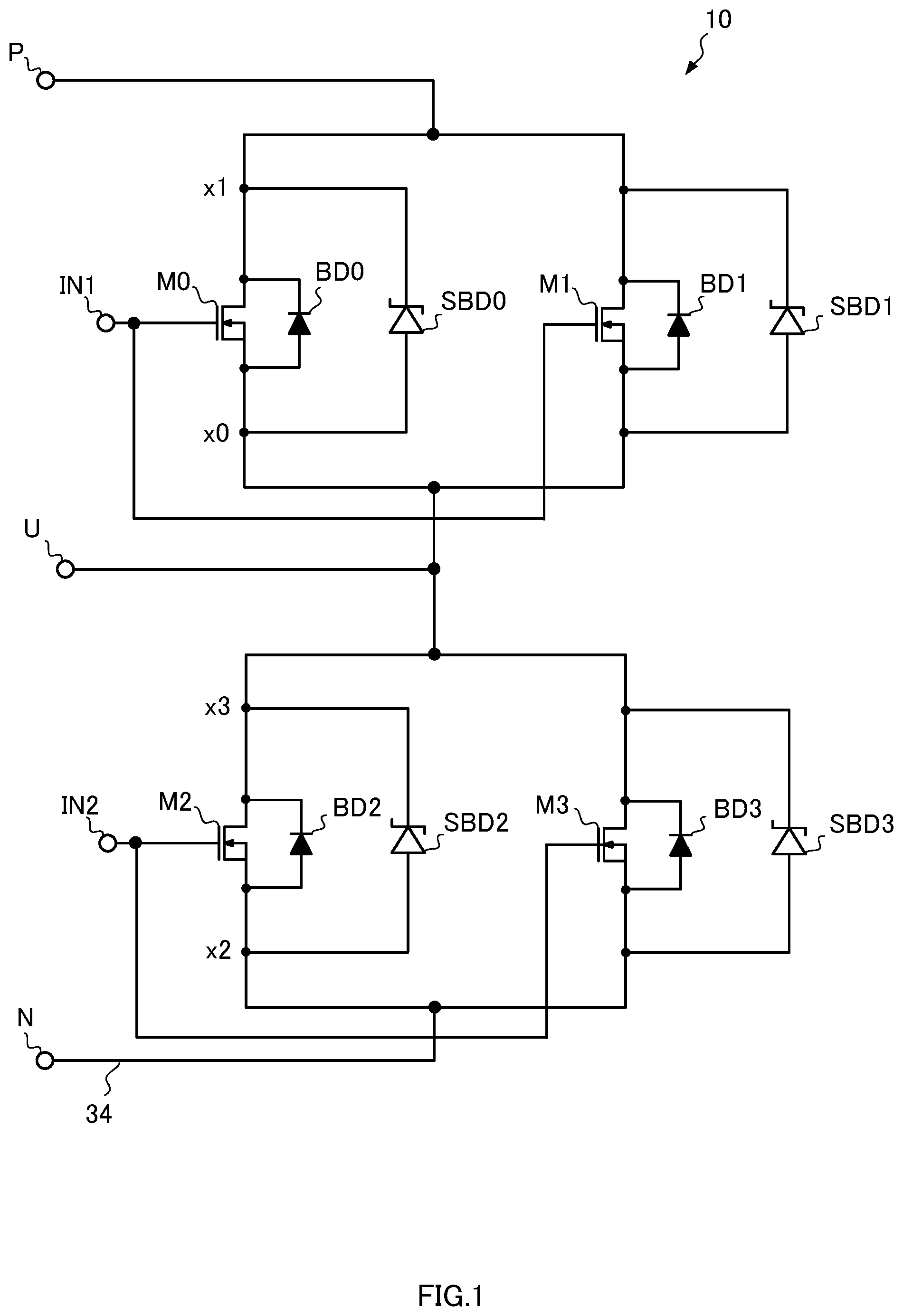
At least following matters will become apparent from the descriptions of the present specification and the accompanying drawings. [Embodiments] <<<Example of Electronic Circuit 10 >>> is a diagram illustrating a configuration of an electronic circuit 10 according to an embodiment of the present disclosure. The electronic circuit 10 is a half-bridge circuit for driving a load (not illustrated) such as a motor coil, and includes n-Type Metal-Oxide-Semiconductor Field-Effect-Transistors (NMOS transistors) M 0 to M 3 , diodes SBD 0 to SBD 3 , a positive electrode terminal P, an output terminal U, a negative electrode terminal N, and control terminals IN 1 and IN 2 . The NMOS transistor M 0 is a switching device of an upper arm having its gate electrode (control electrode) coupled to the control terminal IN 1 of the upper arm, its source electrode coupled to the output terminal U, and its drain electrode coupled to the positive electrode terminal P. The NMOS transistor M 0 also includes a diode BD 0 as a parasitic diode (i.e., a body diode). The NMOS transistor M 1 is a switching device of the upper arm, similarly to the NMOS transistor M 0 , and includes a diode BD 1 . The NMOS transistor M 2 is a switching device of a lower arm having its gate electrode coupled to the control terminal IN 2 of the lower arm, its source electrode coupled to the negative electrode terminal N, and its drain electrode coupled to the output terminal U. The NMOS transistor M 2 includes a diode BD 2 as a parasitic diode. The NMOS transistor M 3 is a switching device of the lower arm, similarly to the NMOS transistor M 2 , and includes a diode BD 3 . Here, in an embodiment of the present disclosure, a MOS transistor is used as the switching device, but the present disclosure is not limited thereto. As the switching device, a Reverse Conducting (RC)-Insulated Gate Bipolar Transistor (IGBT) may be used, which is a reverse conduction type IGBT and includes a bipolar transistor and a diode. In the case of the RC-IGBT, PN junction diodes formed inside may serve as the diodes BD 0 to BD 3 . The diodes BD 0 to BD 3 of an embodiment of the present disclosure are PN junction diodes. The NMOS transistors M 0 to M 3 of an embodiment of the present disclosure are devices manufactured using Silicon Carbide (SiC) which is a wide bandgap semiconductor. Thus, a forward voltage Vf 1 (first voltage) of the diodes BD 0 to BD 3 , which are body diodes, takes a value (for example, 2.5 V) based on the SiC PN junction. A diode SBD 0 is a Schottky barrier diode including a Schottky junction between metal and n-type SiC, and is coupled in anti-parallel to the NMOS transistor M 0 . Diodes SBD 1 to SBD 3 are also SiC Schottky barrier diodes similar to the diode SBD 0 , and are coupled in anti-parallel to the NMOS transistors M 1 to M 3 , respectively. Accordingly, the diodes SBD 0 to SBD 3 operate as free-wheeling diodes. A forward voltage Vf 2 (second voltage) of the diodes SBD 0 to SBD 3 takes a value (for example, 0.7 V) based on the Schottky junction. Although the switching device and the free-wheeling diode are manufactured using SiC in an embodiment of the present disclosure, other wide bandgap semiconductors such as Gallium Nitride (GaN) may also be used. The free-wheeling diode may be a Schottky barrier diode including a Schottky junction of metal and Si. The positive electrode terminal P is a power supply-side (or high-side) terminal, while the negative electrode terminal N is a ground-side (or low-side) terminal. The output terminal U is a terminal to which a load is coupled. A signal for controlling switching of the NMOS transistors M 0 and M 1 , which are the switching devices of the upper arm, is inputted to the control terminal IN 1 . A signal for controlling switching of the NMOS transistors M 2 and M 3 , which are the switching devices of the lower arm, is inputted to the control terminal IN 2 . In the electronic circuit 10 as described above, the switching devices of the upper arm and the switching devices of the lower arm are turned on and off, to thereby drive the load. In the electronic circuit 10 , when the switching devices of the upper arm and the switching devices of the lower arm are simultaneously turned on to drive the load, a large through current flows from the positive electrode terminal P to the negative electrode terminal N. Accordingly, when the load is driven, a dead time period is provided during which the switching devices of the upper arm and the switching devices of the lower arm are both off. In the dead time period, a current may flow from the output terminal U to the positive electrode terminal P, for example. Further, in the dead time period, a current may flow from the negative electrode terminal N to the output terminal U, for example. <<<Current from Output Terminal U to Positive Electrode Terminal P>>> is a diagram for explaining a current flowing through the diodes BD 0 and SBD 0 of the upper arm in the dead time period, for example. In an embodiment of the present disclosure, the current flowing through the diodes BD 0 and SBD 0 is similar to that flowing through the diodes BD 1 and SBD 1 in the dead time period, and thus only the current flowing through the diodes BD 0 and SBD 0 will be described here. A node x 0 in is a node at which a wiring from the output terminal U, a wiring from the source electrode S 1 of the NMOS transistor M 0 , and a wiring from an anode electrode A 0 of the diode SBD 0 are coupled in . Likewise, a node x 1 is a node at which a wiring from the positive electrode terminal P, a wiring from a drain electrode D 1 of the NMOS transistor M 0 , and a wiring from a cathode electrode K 0 of the diode SBD 0 are coupled. Note that, hereinafter, the anode electrode is referred to as anode, and the cathode electrode is referred to as cathode. Here, it is assumed that the wiring between the output terminal U and the node x 0 is a wiring 50 of an inductance La, and that the wiring between the node x 0 and the anode A 0 of the diode SBD 0 is a wiring 51 of an inductance Lb. It is also assumed that the wiring between the positive electrode terminal P and the node x 1 is a wiring 52 of an inductance Lc, and that the wiring between the node x 1 and the cathode K 0 of the diode SBD 0 is a wiring 53 of an inductance Ld. It is further assumed that the wiring between the source electrode S 1 of the NMOS transistor M 0 and the node x 0 is a wiring 54 of an inductance Li, and that the wiring between the drain electrode D 1 of the NMOS transistor M 0 and the node x 1 is a wiring 55 of an inductance Lj. The inductances La to Ld, Li, and Lj are parasitic inductances of the wirings 50 to 55 . Here, as described above, the diode BD 0 is the body diode having the forward voltage Vf 1 (for example, 2.5 V) based on the Sic PN junction, and the diode SBD 0 is the Schottky diode having the forward voltage Vf 2 (for example, 0.7 V) based on the SiC Schottky junction. Thus, the current from the output terminal U first flows to the positive electrode terminal P through a path P 2 indicated by the dashed-dotted line via the diode SBD 0 . In this event, a voltage Vx 01 between the nodes x 0 and x 1 is given by the following expression (1). V × 01 = ( L b + L d ) × d i 2 / d t + V f 2 ( 1 ) In the expression (1), the current flowing through the path P 2 is i 2 , and di 2 /dt is a change with time of the current i 2 flowing through the path P 2 . The change with time of the current i 2 is a value determined based on the current flowing through the load and the time from turning on to turning off of the switching device, for example, which is 0.1 to 10 A/nsec, for example. Here, when the values of the inductances Lb and Ld are small and the voltage Vx 01 does not exceed the forward voltage Vf 1 (for example, 2.5 V), for example, all the current flowing from the output terminal U flows through the path P 2 . As a result, the current i 2 may exceed a rated current of the diode SBD 0 , resulting in breakdown of the diode SBD 0 . Thus, in an embodiment of the present disclosure, the values of the inductances Lb and Ld are increased such that the current from the output terminal U flows to the positive electrode terminal P not only through the path P 2 but also through a path P 1 indicated by the dotted line via the diode BD 0 . The values of the inductances Lb and Ld are calculated based on the relationship given by the expression (2). ( L b + L d ) × d i 2 / d t + V f 2 > ( L i + L j ) × d i 1 / d t + V f 1 ( 2 ) When the expression (2) is modified such that the forward voltage Vf 1 is 2.5 V, the forward voltage Vf 2 is 0.7 V, and di 2 /dt (=di 1 /dt) is 10 A/nsec, the following relational expression (3) is obtained. ( ( L b + L d ) - ( L i + L j ) ) > ( V f 1 - V f 2 ) × d t / d i 2 > ( 2 . 5 - 0 . 7 ) × ( 1 / 1 0 ) > 0.18 ( 3 ) As a result, by setting the sum of the inductances Lb and Ld to be larger than the sum of the inductances Li and Lj, for example, to be larger than 0.18 nH, the currents i 1 and i 2 flow through the paths P 1 and P 2 , respectively, and thus a large current can be avoided from flowing through the diode SBD 0 . As such, in an embodiment of the present disclosure, the inductance of the wiring on the path P 2 is set larger than the inductance of the wiring on the path P 1 such that the diode BD 0 is turned on when the current flows from the output terminal U. As a result, it is possible to reduce the current i 2 flowing through the diode SBD 0 in the currents from the output terminal U, thereby being able to avoid breakdown of the diode SBD 0 . In , three wirings 50 , 51 , and 54 are modeled as the wirings coupled to the node x 0 , for example, but when the node x 0 corresponds to the source electrode S 1 , the inductance Li of the wiring 54 can be ignored, resulting in Li=0. Meanwhile, when the node x 0 corresponds to the output terminal U, for example, the inductance La of the wiring 50 can be ignored, resulting in La=0. Accordingly, although the details will be described later, various semiconductor modules can be represented by equivalent circuits, with the use of the circuit illustrated in . Note here that the diode BD 0 corresponds to a “first diode”, and the diode SBD 0 corresponds to a “second diode”. The output terminal U corresponds to a “first terminal”, and the positive electrode terminal P corresponds to a “second terminal”. The wirings 50 , 52 , 54 , and 55 coupling the output terminal U to the positive electrode terminal P via the diode BD 0 correspond to a “first wiring member”, and the wirings 50 to 53 coupling the output terminal U to the positive electrode terminal P via the diode SBD 0 correspond to a “second wiring member”. Although the forward voltage Vf 1 is 2.5 V and the forward voltage Vf 2 is 0.7 V in an embodiment of the present disclosure, these values are just examples. The values of the forward voltages Vf 1 and Vf 2 and the values of the inductances of the wirings vary depending on the manufacturing variations. In addition, the sum of the required inductances Lb and Ld also changes with the time, current, and temperature used. Thus, the inductance of the “second wiring member” at least has to be larger than the inductance of the “first wiring member”. The inductance of the “second wiring member” is larger than the inductance of the “first wiring member”, preferably, by 0.18 nH or more, more preferably, by 0.36 nH or more. <<Current from Negative Electrode Terminal N to Output Terminal U>> is a diagram for explaining a current flowing through the diodes SBD 2 and BD 2 of the lower arm in the dead time period, for example. In an embodiment of the present disclosure, the current flowing through the diodes BD 2 and SBD 2 is similar to that flowing through the diodes BD 3 and SBD 3 in the dead time period, and thus only the current flowing through the diodes BD 2 and SBD 2 will be described here. A node x 2 in is a node at which a wiring from the negative electrode terminal N, a wiring from a source electrode S 2 of the NMOS transistor M 2 , and a wiring from an anode A 3 of the diode SBD 2 are coupled in . Likewise, a node x 3 is a node at which a wiring from the output terminal U, a wiring from a drain electrode D 2 of the NMOS transistor M 2 , and a wiring from a cathode K 3 of the diode SBD 2 are coupled. Here, it is assumed that the wiring between the negative electrode terminal N and the node x 2 is a wiring 60 of an inductance Le, and that the wiring between the node x 2 and the anode A 3 of the diode SBD 2 is a wiring 61 of an inductance Lf. It is also assumed that the wiring between the output terminal U and the node x 3 is a wiring 62 of an inductance Lg, and that the wiring between the node x 3 and the cathode K 3 of the diode SBD 2 is a wiring 63 of an inductance Lh. It is further assumed that the wiring between the source electrode S 2 of the NMOS transistor M 2 and the node x 2 is a wiring 64 of an inductance Lm, and that the wiring between the drain electrode D 2 of the NMOS transistor M 2 and the node x 3 is a wiring 65 of an inductance Ln. The inductances Le to Lh, Lm, and Ln are parasitic inductances of the wirings 60 to 65 . In an embodiment of the present disclosure, similarly to the upper arm illustrated in , the values of the inductances Lf and Lh are increased such that a current i 3 flows through a path P 3 indicated by the dotted line via the diode BD 2 and a current i 4 flows through a path P 4 indicated by the dashed-dotted line via the diode SBD 2 , upon a current flowing from the negative electrode terminal N. To be more specific, for example, (Lf+Lh)−(Lm+Ln)>0.18 nH holds based on the foregoing expression (3). As a result, when the current flows from the negative electrode terminal N, it is avoided that a large current flowing through the diode SBD 2 of the lower arm resulting in breakdown of the diode SBD 2 . In such a case, the diode BD 2 corresponds to the “first diode”, and the diode SBD 2 corresponds to the “second diode”. The negative electrode terminal N corresponds to the “first terminal”, and the output terminal U corresponds to the “second terminal”. The wirings 60 , 62 , 64 , and 65 coupling the negative electrode terminal N to the output terminal U via the diode BD 2 correspond to the “first wiring member”, and the wirings 60 to 63 coupling the negative electrode terminal N to the output terminal U via the diode SBD 2 correspond to the “second wiring member”. ===Example of Semiconductor Module 80 === is a schematic plan view illustrating an example of a semiconductor module 80 which embodies the electronic circuit 10 . is a schematic diagram for explaining a configuration of the semiconductor module 80 . In an embodiment of the present disclosure, the plurality of switching devices and free-wheeling diodes in the electronic circuit 10 are mounted to the semiconductor module 80 , with the same configuration. Accordingly, for convenience, illustrates only the NMOS transistor M 0 and the diode SBD 0 of the upper arm. The gate electrode G 1 and the source electrode S 1 of the NMOS transistor M 0 are formed on the central axis of the NMOS transistor M 0 , for example, but are illustrated separately here for convenience. Hereinafter, in an embodiment of the present disclosure, “electrically coupled” means that a configuration E 1 and a configuration E 2 are coupled so as to be electrically continuous through a wiring, a bonding material (for example, solder) or the like. This is also simply referred to as “coupling”. This “coupling” includes not only a case where the configuration E 1 is coupled to the configuration E 2 through a wiring member but also a case where the configuration E 1 is coupled to the configuration E 2 through a conductive pattern or the like provided between the configurations E 1 and E 2 . The semiconductor module 80 is a semiconductor device including a plurality of switching devices and free-wheeling diodes of the electronic circuit 10 . In , the switching devices are the NMOS transistors M 0 to M 3 , and the free-wheeling diodes are the diodes SBD 0 to SBD 3 . The semiconductor module 80 includes: laminated substrates 110 and 111 including conductive patterns 210 , 220 , 230 , 310 , 320 , and 330 ; switching devices and free-wheeling diodes arranged in the conductive patterns 220 and 320 ; terminals arranged in conductive patterns 210 , 220 , 310 , 320 , and 330 , and bonding wires electrically coupled to the switching devices and free-wheeling diodes and to the conductive patterns. The semiconductor module 80 may further include a base plate 100 . The terminals each have a prismatic shape, for example, and have one end bonded to the conductive pattern and the other end extending from the semiconductor module 80 to be electrically coupled to an external device (not illustrated). The terminals are made of, for example, copper, aluminum or an alloy containing them. The bonding wires are made of copper, aluminum, gold or an alloy containing them. A member other than the bonding wires can also be used as the wiring member. For example, a lead frame can be used as the wiring member. The base plate 100 has a smooth bonding surface where an insulating circuit board is bonded on its upper surface, and has a rectangular shape in plan view, for example. The base plate 100 is a metal plate made of aluminum, copper, or an alloy containing them, for example. As illustrated in , the laminated substrate 110 is attached to the base plate 100 with a bonding material 101 such as solder provided therebetween. The laminated substrate 111 also has a configuration similar to that of the laminated substrate 110 , and is attached to the same base plate 100 as the laminated substrate 110 is attached to. <<Laminated Substrate 110 on Upper Arm Side>> The laminated substrate 110 includes an insulating plate 200 and conductive patterns 210 , 220 , and 230 formed in the front surface (upper side) of the insulating plate 200 . The insulating plate 200 is made of, for example, ceramics or resin. The conductive patterns 210 , 220 , and 230 are made of, for example, copper, aluminum, or an alloy containing them. The laminated substrate 110 may further include a heat radiation plate 201 on the back surface (lower side) of the insulating plate 200 . The insulating circuit board configured as such is formed of a Direct Copper Bonding (DCB) board or an Active Metal Brazing (AMB) board, for example. In an embodiment of the present disclosure, the laminated substrate 110 is a Direct Bonded Copper (DBC) substrate to which the devices of the upper arm are mounted. <<Conductive Pattern 210 >> The conductive pattern 210 has a control terminal IN 1 mounted thereto, to receive signals for controlling the switching devices of the upper arm. Here, as illustrated in , the control terminal IN 1 is attached to the conductive pattern 210 through a bonding material 252 (for example, solder). The conductive pattern 210 is coupled to the gate electrode G 1 of the NMOS transistor M 0 through a bonding wire (hereinafter, simply referred to as wire), and is coupled to the gate electrode of the NMOS transistor M 1 through a wire. In an embodiment of the present disclosure, in the upper arm, the coupling relationship between the output terminal U, the positive electrode terminal P, and the control terminal IN 1 , and the NMOS transistor M 1 and the diode SBD 1 is the same as that among the NMOS transistor M 0 and the diode SBD 0 , the output terminal U, the positive electrode terminal P, and the control terminal IN 1 . Accordingly, the NMOS transistor M 0 and the diode SBD 0 will be mainly described here. <<Conductive Pattern 220 >> The positive electrode terminal P on the power supply side, the NMOS transistors M 0 and M 1 , and the diodes SBD 0 and SBD 1 are mounted to the conductive pattern 220 . Here, as illustrated in , a drain electrode D 1 formed in the back surface of the NMOS transistor M 0 is attached to the conductive pattern 220 through a bonding material 250 (for example, solder). In an embodiment of the present disclosure, a cathode K 1 of the diode BD 0 is shared with the drain electrode D 1 , which results in the cathode K 1 of the diode BD 0 being also coupled to the conductive pattern 220 . A cathode K 0 of the diode SBD 0 is also attached to the conductive pattern 220 through a bonding material 251 . A positive electrode terminal P is further attached to the conductive pattern 220 through a bonding material. Here, the anode A 0 formed in the front surface of the diode SBD 0 and the source electrode S 1 formed in the front surface of the NMOS transistor M 0 are electrically coupled through a wire W 1 . The anode A 1 of the diode BD 0 is shared with the source electrode S 1 , which results in the anode A 1 of the diode BD 0 being coupled to the anode A 0 of the diode SBD 0 through the wire W 1 . is a diagram for explaining a wiring pattern conceptually generated in the conductive pattern 220 . In the conductive pattern 220 , a current from the cathode K 1 of the diode BD 0 flows along a path P 10 between the cathode K 1 and the positive electrode terminal P, for example. Likewise, a current from the cathode K 0 of the diode SBD 0 flows along a path P 11 between the cathode K 0 and the positive electrode terminal P. Accordingly, wiring patterns corresponding to the paths P 10 and P 11 , respectively, are generated in the conductive pattern 220 . Hereinafter, in an embodiment of the present disclosure, the wiring pattern corresponding to the path P 10 is referred to as wiring pattern C 10 , and the wiring pattern corresponding to the path P 11 is referred to as wiring pattern C 11 . Since the path P 11 is longer than the path P 10 , the wiring pattern C 11 is longer than the wiring pattern C 10 . Accordingly, the wiring pattern C 11 has an inductance larger than that of the wiring pattern C 10 . The NMOS transistor M 1 and the diode SBD 1 are also mounted to the conductive pattern 220 similarly to the NMOS transistor M 0 and the diode SBD 0 , and thus detailed description thereof is omitted here. Further, the “wiring pattern” is a wiring conceptually formed in part of the conductive pattern here, but may also be a wiring that is actually patterned. <<Conductive Pattern 230 >> The conductive pattern 230 in is a pattern electrically coupled to the output terminal U, more specifically, a pattern coupled to a wire from a conductive pattern 320 (to be described later) having the output terminal U mounted thereto. The conductive pattern 230 is coupled to the source electrode S 1 of the NMOS transistor M 0 and the anode A 1 of the diode BD 0 through a wire W 0 . A wire W 1 from the source electrode S 1 is coupled to the anode A 0 of the diode SBD 0 . <<Laminated Substrate 111 on Lower Arm Side>> The laminated substrate 111 is a DBC substrate to which the devices of the lower arm are mounted. The laminated substrate 111 has a configuration similar to that of the laminated substrate 110 , and thus detailed description thereof is omitted. Conductive patterns 310 , 320 , and 330 are formed in the front surface of an insulating plate 300 in the laminated substrate 111 . <<Conductive Pattern 310 >> The conductive pattern 310 has a control terminal IN 2 mounted thereto, to receive signals for controlling the switching devices of the lower arm. The control terminal IN 2 is attached to the conductive pattern 310 through a bonding material (for example, solder). The conductive pattern 310 is coupled to the gate electrode G 2 of the NMOS transistor M 2 through a wire, and is coupled to the gate electrode of the NMOS transistor M 3 through a wire. In the lower arm, the coupling relationship between the output terminal U, the negative electrode terminal N, and the control terminal IN 2 , and the NMOS transistor M 2 and the diode SBD 2 is the same as the coupling relationship between the output terminal U, the negative electrode terminal N, and the control terminal IN 2 , and the NMOS transistor M 3 and the diode SBD 3 . Accordingly, the NMOS transistor M 2 and the diode SBD 2 will be mainly described. <<Conductive Pattern 320 >> An output terminal U, to which a load is to be coupled, NMOS transistors M 2 and M 3 , and diodes SBD 2 and SBD 3 are mounted to the conductive pattern 320 . The coupling relationship between these elements and the conductive pattern 320 is the same as the coupling relationship between the conductive pattern 220 and the NMOS transistor M 0 and the diode SBD 0 described in . To be more specific, the drain electrode D 2 in the back surface side of the NMOS transistor M 2 and the cathode K 2 shared with the drain electrode D 2 are coupled to the conductive pattern 320 through a bonding material. The cathode K 3 formed in the back surface of the diode SBD 2 is also coupled to the conductive pattern 320 through a bonding material. The output terminal U is further attached to the conductive pattern 320 through a bonding material. Here, the anode A 3 formed in the front surface of the diode SBD 2 and the source electrode S 2 formed in the front surface of the NMOS transistor M 2 are electrically coupled through a wire W 3 . The anode A 2 of the diode BD 2 is shared with the source electrode S 2 , which results in the anode A 3 of the diode SBD 2 and the anode A 2 of the diode BD 2 being coupled through the wire W 3 . In this event, a distance from the cathode K 3 of the diode SBD 2 to the output terminal U is longer than a distance from the cathode K 2 of the diode BD 2 to the output terminal U. Accordingly, the wiring pattern from the output terminal U to the diode SBD 2 has an inductance larger than that of the wiring pattern from the output terminal U to the diode BD 2 . Here, the “distance (or path)” from the output terminal U to the cathode K 3 of the diode SBD 2 is determined by, for example, the center of the electrode of the cathode K 3 and the center of the output terminal U. The NMOS transistor M 3 and the diode SBD 3 are coupled to the conductive pattern 320 in a configuration similar to that in which the NMOS transistor M 2 and the diode SBD 2 are coupled thereto, and thus detailed description thereof is omitted here. <<Conductive Pattern 330 >> The conductive pattern 330 has a ground-side negative electrode terminal N mounted thereto. The negative electrode terminal N is attached to the conductive pattern 330 through a bonding material (for example, solder). The conductive pattern 330 is coupled to the source electrode S 2 of the NMOS transistor M 2 through a wire W 2 , and is coupled to the source electrode of the NMOS transistor M 3 through a wire. <<Current from Output Terminal U to Positive Electrode Terminal P>> Here, in the semiconductor module 80 , a current from the output terminal U to the positive electrode terminal P will be described with reference to . The current from the output terminal U flows to the source electrode S 1 of the NMOS transistor M 0 (the anode A 1 of the diode BD 0 ) through the conductive pattern 320 , the wire coupled to the conductive patterns 320 and 230 , the conductive pattern 230 , and the wire W 0 . The current from the wire W 0 is supplied to the anode A 0 of the diode SBD 0 through the wire W 1 . Here, the wiring from the output terminal U to the source electrode S 1 of the NMOS transistor M 0 (the anode A 1 of the diode BD 0 ) can be equivalently represented as a wiring 50 in . The wire W 1 from the source electrode S 1 to the anode A 0 of the diode SBD 0 can be equivalently represented as a wiring 51 . The configurations and components denoted by the same reference numerals are the same between . A current supplied to the anode A 1 of the diode BD 0 flows to the positive electrode terminal P through the cathode K 1 in the back surface and a wiring pattern C 10 in . The current supplied to the anode A 0 of the diode SBD 0 flows to the positive electrode terminal P through the cathode K 0 in the back surface and a wiring pattern C 11 in . Here, the wiring pattern C 10 from the cathode K 1 to the positive electrode terminal P can be equivalently represented as a wiring 55 in , and the wiring pattern C 11 from the cathode K 0 to the positive electrode terminal P can be equivalently represented as a wiring 53 . Then, in an embodiment of the present disclosure, the inductance of the wiring on the path P 2 in is increased such that the conditions of the expression (3) are satisfied. More specifically, for example, the inductances Lb and Ld are increased such that the difference between the inductance (La+Lb+Ld) on the path P 2 and the inductance (La+Lj) on the path P 1 is 0.18 nH or more. As a result, the current it supplied to the source electrode S 1 in the front surface of the NMOS transistor M 0 (the anode A 1 of the diode BD 0 ), in the currents from the output terminal U, flows from the anode A 1 in the front surface of the diode BD 0 to the cathode K 1 in the back surface through the diode BD 0 , and then flows to the positive electrode terminal P through the wiring pattern C 10 in the conductive pattern 220 . The current i 2 supplied to the anode A 0 in the front surface of the diode SBD 0 also flows from the anode A 0 in the front surface of the diode SBD 0 to the cathode K 0 in the back surface through the diode SBD 0 , and then flows to the positive electrode terminal P through the wiring pattern C 11 in the conductive pattern 220 . As such, in an embodiment of the present disclosure, even if a large current may flow from the output terminal U, currents flow through both the diodes BD 0 and SBD 0 . This can avoid breakdown of the diode SBD 0 . In the semiconductor module 80 , the wiring member (for example, the wire W 0 and the wiring pattern C 10 in the conductive pattern 220 ) provided on the path P 1 corresponds to the “first wiring member”, and the wiring member (for example, the wires W 0 and W 1 and the wiring pattern C 11 in the conductive pattern 220 ) provided on the path P 2 corresponds to the “second wiring member”. <<Current from Negative Electrode Terminal N to Output Terminal U>> Next, in the semiconductor module 80 , the current from the negative electrode terminal N to the output terminal U will be described with reference to . The current from the negative electrode terminal N flows to the source electrode S 2 of the NMOS transistor M 2 (the anode A 2 of the diode BD 2 ) through the conductive pattern 330 and the wire W 2 . The current from the wire W 2 is supplied to the anode A 3 of the diode SBD 2 through the wire W 3 . Here, the wire W 2 coupling the negative electrode terminal N and the source electrode S 2 of the NMOS transistor M 2 (the anode A 2 of the diode BD 2 ) can be equivalently represented as a wiring 60 in . The wire W 3 coupling the source electrode S 2 of the NMOS transistor M 2 and the anode A 3 of the diode SBD 2 can be equivalently represented as a wiring 61 in . Similarly to , the wiring pattern from the cathode K 2 to the output terminal U can be equivalently represented as a wiring 65 , and the wiring pattern from the cathode K 3 to the output terminal U can be equivalently represented as a wiring 63 . In an embodiment of the present disclosure, the inductance of the wiring on the path P 4 is increased such that the conditions of the expression (3) are satisfied. More specifically, for example, the inductances Lf and Lh are increased such that the difference between the inductance (Le+Lf+Lh) on the path P 4 and the inductance (Le+Ln) on the path P 3 is 0.18 nH or more. Thus, the current i 3 supplied to the source electrode S 2 in the front surface of the NMOS transistor M 2 (the anode A 2 of the diode BD 2 ), in the currents from the negative electrode terminal N, flows from the anode A 2 in the front surface of the diode BD 2 to the cathode K 2 in the back surface through the diode BD 2 , and then flows to the output terminal U through a wiring pattern (not illustrated) in the conductive pattern 320 . The current i 4 supplied to the anode A 3 in the front surface of the diode SBD 2 also flows from the anode A 3 in the front surface of the diode SBD 2 to the cathode K 3 in the back surface through the diode SBD 2 , and then flows to the output terminal U through the wiring pattern (not illustrated) in the conductive pattern 320 . As a result, in an embodiment of the present disclosure, even when a large current may flow from the negative electrode terminal N, currents flow through both the diodes BD 2 and SBD 2 . This can avoid breakdown of the diode SBD 2 . ===Other Embodiments=== Here, for example, in order to avoid breakdown of the diode SBD 0 of the upper arm caused by the current, at least one of the inductance Lb of the wiring 51 and the inductance Ld of the wiring 53 in has only to be increased. <<When Wiring 51 is Realized with Wire>> When the wiring 51 is realized with a wire, the inductance Lb can be increased by increasing the length of the wire, by reducing the cross-sectional area of the wire, or by increasing the curvature of the wire. <<Adjusting Wire Length>> is a diagram for explaining an embodiment in which the length of the wire is adjusted. In , the configurations and components denoted by the same reference numerals as those in are the same. Thus, a wire W 10 to the NMOS transistor M 0 and a wire W 11 to the diode SBD 0 will be mainly described here. In , it is assumed that the diode SBD 0 is mounted at a position away from the NMOS transistor M 0 in the conductive pattern 220 . The wire W 10 couples the conductive pattern 230 electrically coupled to the output terminal U and the source electrode S 1 of the NMOS transistor M 0 (the anode A 1 of the diode BD 0 ). The wire W 11 is longer than the wire W 10 , and couples the conductive pattern 230 to the anode A 0 of the diode SBD 0 . Since the wires W 10 and W 11 are the same (for example, in cross-sectional area and curvature) except for the length, the wire W 11 has an inductance larger than that of the wire W 10 . is a diagram illustrating the configuration of using an equivalent circuit. Here, the wiring including the conductive pattern 230 and the wire W 10 coupling the output terminal U to the source electrode S 1 of the NMOS transistor M 0 (the anode A 1 of the diode BD 0 ) can be equivalently represented as a wiring 54 . The wire W 11 coupling the output terminal U to the anode A 0 of the diode SBD 0 can be equivalently represented as a wiring 51 . The wiring pattern from the cathode K 1 of the diode BD 0 to the positive electrode terminal P can be equivalently represented as a wiring 55 , and the wiring pattern from the cathode K 0 of the diode SBD 0 to the positive electrode terminal P can be equivalently represented as a wiring 53 . In such an embodiment, the inductance on the path P 2 (Lb+Ld) is set larger than the inductance on the path P 1 (Li+Lj), and the length of the wire W 11 is increased such that the expression (3) is satisfied, for example. As a result, even when a large current flows from the output terminal U, breakdown of the diode SBD 0 can be avoided. Here, the wire W 10 corresponds to the “first wire”, and the wire W 11 corresponds to the “second wire”. <<Adjusting Cross-Sectional Area of Wire> is a diagram for explaining an embodiment in which the cross-sectional area of the wire is adjusted. In , the configurations and components denoted by the same reference numerals as those in are the same. Thus, a wire W 20 to the NMOS transistor M 0 and a wire W 21 to the diode SBD 0 will be mainly described. The wire W 20 has a larger cross-sectional area (i.e., thicker) than the wire W 21 , and couples the conductive pattern 230 coupled to the output terminal U and the source electrode S 1 of the NMOS transistor M 0 and the anode A 1 of the diode BD 0 . For example, the wire W 20 has a diameter of 400 μm and the wire W 21 has a diameter of 250 μm. The wire W 21 couples the conductive pattern 230 and the anode A 0 of the diode SBD 0 . Since the wires W 20 and W 21 are the same (for example, in length and curvature) except for the cross-sectional area, the wire W 21 has an inductance larger than that of the wire W 20 . Since the coupling relationship between the output terminal U and the positive electrode terminal P in is the same as the coupling relationship between the output terminal U and the positive electrode terminal P in , an equivalent circuit according to such an embodiment of is also as illustrated in . The inductance Lb is increased as the cross-sectional area of the wire W 21 is reduced, and thus breakdown of the diode SBD 0 can be avoided. Here, the number of the wires W 20 ( 4 wires) corresponds to the number of the wires W 21 ( 4 wires), meanwhile the wires W 21 each having a smaller cross-sectional area are used. However, the present disclosure is not limited thereto. For example, even when the wires W 20 and W 21 having the same cross-sectional area are used and the number of the wires W 21 is set smaller than that of the wires W 20 , the same effect as that of an embodiment of the present disclosure can be achieved. Here, the wire W 20 corresponds to the “first wire”, and the wire W 21 corresponds to the “second wire”. <<Adjusting Curvature of Wire>> is a diagram for explaining an embodiment in which the curvature of the wire is adjusted. In , the configurations and components denoted by the same reference numerals as those in are the same. Thus, a wire W 30 to the NMOS transistor M 0 and a wire W 31 to the diode SBD 0 will be mainly described here. The wire W 30 couples the conductive pattern 230 coupled to the output terminal U and the source electrode S 1 of the NMOS transistor M 0 and the anode A 1 of the diode BD 0 . The wire W 31 has a larger curvature than the wire W 30 , and couples the conductive pattern 230 and the anode A 0 of the diode SBD 0 . As the curvature (degree of bending) of the wire W 31 is increased, the length of the wire W 31 is also increased. Here, for example, since the wires W 30 and W 31 have the same cross-sectional area, the wire W 31 has an inductance larger than that of the wire W 30 . Since the coupling relationship between the output terminal U and the positive electrode terminal P in is the same as the coupling relationship between the output terminal U and the positive electrode terminal P in , an equivalent circuit according to such an embodiment of is also as illustrated in . The inductance Lb is increased as the curvature of the wire W 31 is increased, for example, and thus breakdown of the diode SBD 0 can be avoided. Here, the wire W 30 corresponds to the “first wire”, and the wire W 31 corresponds to the “second wire”. <<When Wiring 53 is Realized with Wiring Pattern>> Next, a description will be given of a case where the wiring 53 in is realized with a wiring pattern. Here, when the wiring 53 is realized with a wiring pattern, the inductance Ld can be increased, for example, by increasing the length of the wiring pattern, by reducing the thickness of the wiring pattern, or by reducing the width of the wiring pattern. The description has already been given, with reference to , of the case where the inductance Ld is increased by increasing the length of the wiring pattern. Accordingly, the remaining two methods will be described here. <<Adjusting Thickness and Width of Wiring Pattern>> are diagrams for explaining an embodiment in which the thickness and width of a wiring pattern are adjusted. In , the configurations and components denoted by the same reference numerals as those in are the same. Thus, conductive patterns 270 and 280 and wires W 40 to W 42 will be described here. The positive electrode terminal P on the power supply side and the NMOS transistor M 0 are mounted to the conductive pattern 270 . The conductive pattern 280 is thinner than the conductive pattern 270 , and has the diode SBD 0 mounted thereto. In the conductive pattern 280 , a width Wx of a region between a region in which the diode SBD 0 is mounted and a region in which the wire W 40 is coupled is reduced. The conductive patterns 270 and 280 are coupled with the wire W 40 . The wire W 41 couples the conductive pattern 230 electrically coupled to the output terminal U and the source electrode S 1 of the NMOS transistor M 0 (the anode A 1 of the diode BD 0 ). The wire W 42 couples the source electrode S 1 of the NMOS transistor M 0 (the anode A 1 of the diode BD 0 ) and the anode A 0 of the diode SBD 0 . Here, a current from the conductive pattern 230 electrically coupled to the output terminal U flows to the source electrode S 1 (anode A 1 ) through the wire W 41 . Then, the current from the source electrode S 1 flows to the anode A 0 through the wire W 42 . The current from the anode A 1 flows to the positive electrode terminal P through the diode BD 0 , the cathode K 1 in the back surface side, and the wiring pattern C 21 in the conductive pattern 270 . The current from the anode A 0 flows to the positive electrode terminal P through the diode SBD 0 , the cathode K 2 in the back surface side, the wiring pattern C 20 , the wire W 40 , and the conductive pattern 270 . Accordingly, an embodiment of can be represented by the equivalent circuit illustrated in , similarly to an embodiment of . In an embodiment of the present disclosure, the conductive pattern 280 having the path P 20 formed therein is thinner than the conductive pattern 270 , and the width Wx of the path P 20 is also smaller. Thus, the wiring pattern C 20 conceptually formed on the path P 20 has an inductance larger than that of the wiring pattern C 21 conceptually formed on the path P 21 . Accordingly, by using the wiring pattern C 20 having a large inductance, the inductance Ld of the wiring 53 in can be increased. As a result, the use of the configuration illustrated in makes it possible to avoid breakdown of the diode SBD 0 . <<Other Configuration Examples of Part of Semiconductor Modules>> is a diagram illustrating a configuration of elements of an upper arm of a semiconductor module. The configurations denoted by the same reference numerals in are the same. Thus, conductive patterns 290 and 291 and wires W 50 and W 51 will be mainly described here. The conductive pattern 290 has the output terminal U mounted thereto, and the wire W 50 couples the conductive pattern 290 to the source electrode S 1 of the NMOS transistor M 0 (the anode A 1 of the diode BD 0 ). The conductive pattern 291 has the positive electrode terminal P, the NMOS transistor M 0 , and the diode SBD 0 mounted thereto. The wire W 51 couples the source electrode S 1 of the NMOS transistor M 0 (the anode A 1 of the diode BD 0 ) to the anode A 0 of the diode SBD 0 . is a diagram illustrating the configuration of in an equivalent circuit. Here, the wiring including the conductive pattern 290 and the wire W 50 coupling the output terminal U to the source electrode S 1 of the NMOS transistor M 0 (the anode A 1 of the diode BD 0 ) can be equivalently represented as a wiring 50 . The wire W 51 coupling the source electrode S 1 of the NMOS transistor M 0 (anode A 1 of the diode BD 0 ) and the anode A 0 of the diode SBD 0 can be equivalently represented as the wiring 51 . The wiring pattern from the cathode K 0 of the diode SBD 0 to the cathode K 1 of the diode BD 0 can be equivalently represented as a wiring 53 , and the wiring pattern from the cathode K 1 of the diode BD 0 to the positive electrode terminal P can be equivalently represented as a wiring 52 . In such an embodiment, the inductance on the path P 2 (La+Lb+Lc+Ld) is larger than the inductance on the path P 1 (La+Lc) without fail. In an embodiment of the present disclosure, the length of the wire W 51 is increased, for example, such that the relationship of Lb+Ld>0.18 nH is satisfied, for example. As a result, even when a large current flows from the output terminal U, breakdown of the diode SBD 0 can be avoided. Here, the wire W 50 corresponds to the “first wire”, and the wires W 50 and W 51 correspond to the “second wire”. is a diagram illustrating a configuration of elements of a lower arm of a semiconductor module. The configurations and components denoted by the same reference numerals are the same between . Thus, conductive patterns 340 and 341 and wires W 60 and W 61 will be mainly described here. The conductive pattern 340 has the negative electrode terminal N mounted thereto, and the wire W 60 couples the conductive pattern 340 to the source electrode S 2 of the NMOS transistor M 2 (the anode A 2 of the diode BD 2 ). The wire W 61 couples the conductive pattern 340 to the anode A 3 of the diode SBD 2 . The conductive pattern 341 has the output terminal U, the NMOS transistor M 2 , and the diode SBD 2 mounted thereto. is a diagram illustrating the configuration of in an equivalent circuit. Here, the wiring pattern conceptually formed from the negative electrode terminal N to a position O in the conductive pattern 340 can be equivalently represented as a wiring 60 . The position O is a position at which the current from the negative electrode terminal N is conceptually divided into the NMOS transistor M 2 and the diode SBD 2 in the conductive pattern 340 , and corresponds to the node x 2 . The wiring including the wiring pattern from the position O to the source electrode S 2 of the NMOS transistor M 2 (the anode A 2 of the diode BD 2 ) and the wire W 60 can be equivalently represented as a wiring 64 . The wiring including the wiring pattern from the position O to the anode A 3 of the diode SBD 2 and the wire W 61 can be equivalently represented as a wiring 61 . The wiring pattern from the cathode K 3 of the diode SBD 2 to the cathode K 2 of the diode BD 2 can be equivalently represented as a wiring 63 . The wiring pattern from the cathode K 2 of the diode BD 2 to the output terminal U can be equivalently represented as a wiring 62 . In such an embodiment, the length of the wire W 61 is increased, for example, such that the inductance on the path P 4 (Le+Lf+Lg+Lh) is larger than the inductance on the path P 3 (Le+Lm+Lg). As a result, even when a large current flows from the negative electrode terminal N, breakdown of the diode SBD 2 can be avoided. In an embodiment of the present disclosure, it is preferable that (Lf+Lh)−Lm>0.18 nH is satisfied, and it is more preferable that (Lf+Lh)−Lm>0.36 nH is satisfied. Accordingly, with (Lf+Lh) being set larger, even when there are variations in the characteristics of the elements and/or the inductance of the wire W 60 , for example, the current flowing through the diode SBD 2 can be reduced. ===Summary=== The electronic circuit 10 and the semiconductor module 80 according to an embodiment of the present disclosure have been described above. As illustrated in , the inductance on the path P 2 is larger than the inductance on the path P 1 in the electronic circuit 10 . Thus, the current from the output terminal U flows not only through the diode SBD 0 on the path P 2 but also through the diode BD 0 on the path P 1 . Accordingly, in the electronic circuit 10 , it is avoided that a large current flowing through the diode SBD 0 , which is a free-wheeling diode, resulting in breakdown of the diode SBD 0 . A general bipolar transistor may be used as the switching device. And, with a PN diode having a PN junction and a Schottky diode having a Schottky junction being coupled, as free-wheeling diodes, to the bipolar transistor, the same effect as that in an embodiment of the present disclosure can be achieved. However, in an embodiment of the present disclosure, the NMOS transistor M 0 is used as the switching device. Thus, the parasitic diode (body diode) of the NMOS transistor M 0 can be used as the free-wheeling diode without separately providing the PN diode. The NMOS transistor M 0 and the diode SBD 0 having a Schottky junction are elements using a wide bandgap semiconductor. Thus, in an embodiment of the present disclosure, it is possible to reduce the loss in driving the load, while improving the withstand voltage of the electronic circuit 10 . The diode SBD 0 having a Schottky junction is coupled in anti-parallel to the NMOS transistor M 0 such that the diode can operate as a free-wheeling diode when the NMOS transistor M 0 is off. The semiconductor module 80 is a device including the electronic circuit 10 in which the inductance on the path P 2 through the SBD 0 is larger than the inductance on the path P 1 through the NMOS transistor M 0 . Accordingly, when such a semiconductor module 80 is used, the diode SBD 0 having a Schottky junction can be protected from a large current. In the semiconductor module 80 , as illustrated in , the wire W 0 from the conductive pattern 230 is coupled to the diode BD 0 having a PN junction, and the wire W 1 from the diode BD 0 is coupled to the diode SBD 0 having a Schottky junction. Accordingly, the inductance from the conductive pattern 230 to the diode SBD 0 can be set larger than the inductance from the conductive pattern 230 to the diode BD 0 . As illustrated in , the conductive pattern 230 and the diode SBD 0 may be coupled by using the wire W 11 longer than the wire W 10 . In such a case as well, the inductance from the conductive pattern 230 to the diode SBD 0 can be set larger than the inductance from the conductive pattern 230 to the diode BD 0 . As illustrated in , the conductive pattern 230 and the diode SBD 0 may be coupled by using the wire W 21 having a cross-sectional area smaller than that of the wire W 20 . In such a case as well, the inductance from the conductive pattern 230 to the diode SBD 0 can be set larger than the inductance from the conductive pattern 230 to the diode BD 0 . As illustrated in , the conductive pattern 230 and the diode SBD 0 may be coupled by using the wire W 31 having a curvature larger than that of the wire W 30 . In such a case as well, the inductance from the conductive pattern 230 to the diode SBD 0 can be set larger than the inductance from the conductive pattern 230 to the diode BD 0 . Further, in the semiconductor module 80 , the U terminal (or the conductive pattern 230 coupled to the U-terminal), the NMOS transistor M 0 , and the diode SBD 0 are arranged in this order along the longitudinal direction (predetermined direction) of the semiconductor module 80 . In other words, the NMOS transistor M 0 is provided between the U-terminal and the diode SBD 0 . If the U-terminal, the diode SBD 0 , and the NMOS transistor M 0 are arranged in this order along the longitudinal direction, generally, the inductance of the wiring from the output terminal U to the diode SBD 0 is smaller than that of the wiring from the U-terminal to the diode BD 0 . However, with the elements and the like being arranged in the order in an embodiment of the present disclosure, the inductance of the wiring from the U-terminal to the diode SBD 0 can be set larger than the inductance of the wiring from the U-terminal to the diode BD 0 serving as a parasitic element. Further, in the semiconductor module 80 , the wire W 0 , in the wires (for example, the wires W 0 and W 1 ) coupling the U-terminal to the diode SBD 0 , is used as a wire coupling the U-terminal to the diode BD 0 . In such a case, the inductance of the wire coupling the U-terminal to the diode SBD 0 is larger than the inductance of the wire coupling the U-terminal to the diode BD 0 without fail. Note that, in the semiconductor module 80 , the wires W 0 and W 1 correspond to the “second wire”, and the wire W 0 corresponds to the “first wire”. For example, in order to increase the inductance on the path P 2 , the inductance of the wiring pattern, instead of the wire, may be increased. In such a case as well, the diode SBD 0 can be protected. As illustrated in , when the path P 2 includes the wiring pattern C 11 longer than the wiring pattern C 10 , the inductance on the path P 2 can be increased. Note that, the wiring pattern C 10 corresponds to the “first wiring pattern”, and the wiring pattern C 11 corresponds to the “second wiring pattern”. For example, as illustrated in , the thickness of the conceptually formed wiring pattern C 20 may be set smaller than the thickness of the wiring pattern C 21 . In such a case as well, the inductance on the path P 2 can be increased. As illustrated in , for example, in a case where the width Wx of the wiring pattern C 20 is reduced as well, the inductance on the path P 2 can be increased. As illustrated in , the wiring pattern C 10 is determined based on the distance between the positive electrode terminal P and the diode BD 0 in the conductive pattern 220 , and the wiring pattern C 11 is determined based on the distance between the positive electrode terminal P and the diode BD 0 in the conductive pattern 220 . Further, in the semiconductor module 80 , the conductive pattern 220 having the positive electrode terminal P mounted thereto is provided between the conductive pattern 210 having the control terminal IN 1 mounted thereto and the conductive pattern 230 electrically coupled to the output terminal U. The conductive pattern 220 corresponds to the “first conductive pattern”, the conductive pattern 230 corresponds to the “second conductive pattern”, and the conductive pattern 210 corresponds to the “third conductive pattern”. The present disclosure is directed to provision of an electronic circuit and a semiconductor module capable of avoiding breakdown of a free-wheeling diode. According to the present disclosure, it is possible to provide an electronic circuit and a semiconductor module capable of avoiding breakdown of a free-wheeling diode. Embodiments of the present disclosure described above are simply to facilitate understanding of the present disclosure and are not in any way to be construed as limiting the present disclosure. The present disclosure may variously be changed or altered without departing from its essential features and encompass equivalents thereof.
Figures (20)
Citations
This patent cites (23)
- US2003/0137320
- US2009/0206812
- US2011/0062491
- US2013/0082284
- US2014/0001481
- US2014/0264376
- US2015/0023081
- US2015/0223339
- US2017/0213806
- US2019/0103866
- US2019/0273489
- US2020/0185359
- US2021/0320045
- US102067309
- US104134663
- US104919589
- US2003-536363
- US2009-195054
- US2011-250589
- US2014225706
- US2017130621
- US2020-009834
- US2019044748