Abstract
According to one embodiment, a semiconductor device includes a first conductive layer between first and second insulating layers with an oxide semiconductor column extending in the first direction through these layers. A third insulating layer covers the column. The column has a first semiconductor portion at a first position matching the first insulating layer, a second semiconductor portion at a second position matching second insulating layer, and a third semiconductor portion at a third position matching the first conductive layer. The first semiconductor portion is continuous along a second direction between the third insulating layer, the second semiconductor portion is continuous along the second direction between the third insulating layer, but the third semiconductor portion is not continuous between the third insulating layer.
Claims (20)
1 . A semiconductor device, comprising: a first insulating layer; a second insulating layer spaced from the first insulating layer in a first direction; a first conductive layer between the first insulating layer and the second insulating layer in the first direction; an oxide semiconductor layer extending in the first direction and facing the first insulating layer, the second insulating layer, and the first conductive layer in a second direction perpendicular to the first direction; and a third insulating layer that is between the first insulating layer and the oxide semiconductor layer, the second insulating layer and the oxide semiconductor layer, and the first conductive layer and the oxide semiconductor layer, wherein the oxide semiconductor layer includes: a first semiconductor portion at a first position along the first direction corresponding to the first insulating layer, a second semiconductor portion at a second position along the first direction corresponding to the second insulating layer, and a third semiconductor portion at a third position along the first direction corresponding to the first conductive layer, and in a first cross-section along in the first direction and the second direction: the first semiconductor portion is continuous along the second direction between opposite sides contacting the third insulating layer, the second semiconductor portion is continuous along the second direction between sides contacting the third insulating layer, and the third semiconductor portion is not continuous along the second direction between a first portion contacting the third insulating layer on one side of the third semiconductor portion and a second portion spaced in the second direction from the first portion and contacting the third semiconductor layer on an opposite side of the third semiconductor portion.
9 . A semiconductor device, comprising: a first insulating layer; a second insulating layer spaced from the first insulating layer in a first direction; a first conductive layer between the first insulating layer and the second insulating layer in the first direction; an oxide semiconductor layer extending in the first direction and facing the first insulating layer, the second insulating layer, and the first conductive layer in a second direction perpendicular to the first direction; and a third insulating layer that is between the first insulating layer and the oxide semiconductor layer, the second insulating layer and the oxide semiconductor layer, and the first conductive layer and the oxide semiconductor layer, wherein the oxide semiconductor layer includes: a first semiconductor portion at a first position along the first direction corresponding to the first insulating layer, a second semiconductor portion at a second position along the first direction corresponding to the second insulating layer, and a third semiconductor portion at a third position along the first direction corresponding to the first conductive layer, and in a first cross-section along the first direction and the second direction: the first semiconductor portion has: a first surface that is in contact with the third insulating layer on one side of the first semiconductor portion, and a second surface that is in contact with the third insulating layer on another side of the first semiconductor portion, the second semiconductor portion has: a third surface that is in contact with the third insulating layer on one side of the second semiconductor portion, and a fourth surface that is in contact with the third insulating layer on another side of the second semiconductor portion, the third semiconductor portion has: a first portion and a second portion spaced from each other in the second direction, a fifth surface that is in contact with the third insulating layer on one side of the third semiconductor portion, and a sixth surface that is in contact with the third insulating layer on another side of the third semiconductor portion, a distance from the fifth surface to the sixth surface is greater than a distance from the first surface to the second surface, and the distance from the fifth surface to the sixth surface is greater than a distance from the third surface to the fourth surface.
18 . A semiconductor memory device, comprising: a first wiring layer; a second wiring layer spaced from the first wiring layer in a first direction; a third wiring layer between the first and second wiring layers in the first direction; a first insulating layer between the first wiring layer and the third wiring layer in the first direction; a second insulating layer between the second wiring layer and the third wiring layer in the first direction; an oxide semiconductor column extending in the first direction from the first wiring layer to second wiring layer through the first insulating layer, the third wiring layer, and the second insulating layer; a third insulating layer on the oxide semiconductor column between the oxide semiconductor column between each of the first insulating layer, the third wiring layer, and the second insulating layer in a second direction perpendicular to the first direction, wherein an outer dimension of the oxide semiconductor column in the second direction is at a maximum at a position along the first direction corresponding to the third wiring layer, and a cavity is inside the oxide semiconductor column at the position along the position along the first direction corresponding to the third wiring layer.
Show 17 dependent claims
2 . The semiconductor device according to claim 1 , wherein the first semiconductor portion, in the first cross-section, includes: a first surface that is in contact with the third insulating layer on one side of the first semiconductor portion, and a second surface that is in contact with the third insulating layer on an opposite side of the first semiconductor portion, the second semiconductor portion, in the first cross-section includes: a third surface that is in contact with the third insulating layer on one side of the second semiconductor portion, and a fourth surface that is in contact with the third insulating layer on an opposite side of the second semiconductor portion, the third semiconductor portion, in the first cross-section includes: a fifth surface that is in contact with the third insulating layer on one side of the third semiconductor portion, and a sixth surface that is in contact with the third insulating layer on an opposite side of the third semiconductor portion, a distance from the fifth surface to the sixth surface is greater than a distance from the first surface to the second surface, and the distance from the fifth surface to the sixth surface is greater than a distance from the third surface to the fourth surface.
3 . The semiconductor device according to claim 1 , wherein the oxide semiconductor layer further includes: a fourth semiconductor portion corresponding in position along the first direction to the first insulating layer, the fourth semiconductor portion being a fourth position between the first position and the third position along the first direction, and the fourth semiconductor portion, in the first cross-section, includes a third portion and a fourth portion spaced from each other in the second direction and in contact with the third insulating layer.
4 . The semiconductor device according to claim 3 , wherein the oxide semiconductor layer further includes: a fifth semiconductor portion corresponding in position along the first direction to the second insulating layer, the fifth semiconductor portion being at a fifth position between the second position and the third position along the first direction, and the fifth semiconductor portion, in the first cross-section, includes a fifth portion and a sixth portion spaced from each other in the second direction and in contact with the third insulating layer.
5 . The semiconductor device according to claim 1 , wherein a cavity is between the first portion and the second portion.
6 . The semiconductor device according to claim 5 , wherein, in a second cross-section orthogonal to the first direction, the third semiconductor portion surrounds the cavity.
7 . The semiconductor device according to claim 1 , further comprising: a second conductive layer connected to one end of the second semiconductor portion in the first direction, wherein the second conductive layer comprises indium and tin.
8 . The semiconductor device according to claim 7 , further comprising: a third conductive layer connected to one end of the first semiconductor portion in the first direction, wherein the third conductive layer comprises indium and tin.
10 . The semiconductor device according to claim 9 , wherein a cavity is between the first portion and the second portion.
11 . The semiconductor device according to claim 10 , wherein, in a second cross-section orthogonal to the first direction, the third semiconductor portion surrounds the cavity.
12 . The semiconductor device according to claim 9 , further comprising: a second conductive layer connected to one end of the second semiconductor portion in the first direction, wherein the second conductive layer comprises indium and tin.
13 . The semiconductor device according to claim 12 , further comprising: a third conductive layer connected to one end of the first semiconductor portion in the first direction, wherein the third conductive layer comprises indium and tin.
14 . The semiconductor device according to claim 9 , wherein the first semiconductor portion includes a seventh portion and an eighth portion spaced from each other in the second direction, a fourth insulating layer is between the seventh portion and the eighth portion in the second direction, and a fifth insulating layer is between the first portion and the second portion in the second direction.
15 . The semiconductor device according to claim 14 , wherein a width of the fifth insulating layer in the second direction is greater than a width of the fourth insulating layer in the second direction.
16 . The semiconductor device according to claim 14 , wherein the third semiconductor portion surrounds the fifth insulating layer in a plane orthogonal to the first direction.
17 . The semiconductor device according to claim 14 , wherein the oxide semiconductor layer further includes: a fifth semiconductor portion corresponding to in position along the first direction to the second insulating layer, the fifth semiconductor portion being at a fifth position between the second position and the third position along the first direction, the fifth semiconductor portion, in the first cross-section, includes a ninth portion and a tenth portion spaced from each other in the second direction, and a sixth insulating layer is between the ninth portion and the tenth portion I the second direction.
19 . The semiconductor memory device according to claim 18 , wherein the cavity is filled with an insulating material.
20 . The semiconductor memory device according to claim 18 , wherein the cavity is present inside the oxide semiconductor column at positions along the first direction corresponding to the first insulating layer.
Full Description
Show full text →
CROSS-REFERENCE TO RELATED APPLICATION
This application is based upon and claims the benefit of priority from Japanese Patent Application No. 2022-148833, filed Sep. 20, 2022, the entire contents of which are incorporated herein by reference. FIELD Embodiments described herein relate generally to a semiconductor device.
BACKGROUND
A semiconductor device with a first insulating layer and a second insulating layer located in a first direction, a first conductive layer between the first insulating layer and the second insulating layer, and an oxide semiconductor layer extending in the first direction and facing the first insulating layer, the second insulating layer, and the first conductive layer is known.
BRIEF DESCRIPTION OF THE DRAWINGS
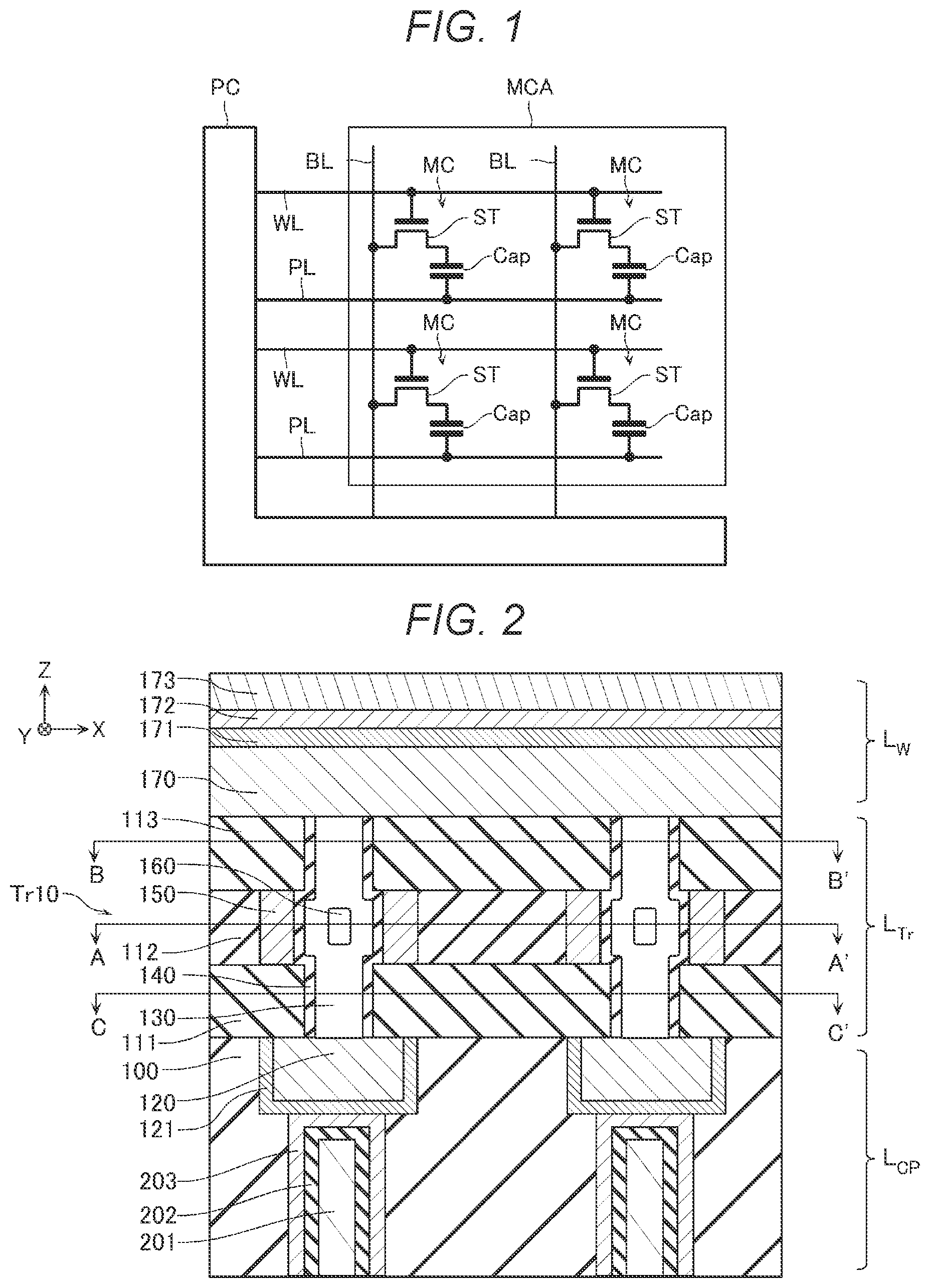
is a schematic circuit diagram illustrating aspects of a semiconductor device according to a first embodiment. is a schematic cross-sectional view illustrating aspects of a semiconductor device according to a first embodiment. is a schematic plan view illustrating aspects of a semiconductor device according to a first embodiment. is a schematic plan view aspects of a semiconductor device according to a first embodiment. is a schematic plan view aspects of a semiconductor device according to a first embodiment. is a schematic cross-sectional view illustrating aspects of a semiconductor device according to a first embodiment. to 14 depict aspects of a method of manufacturing a semiconductor device according to a first embodiment. is a schematic cross-sectional view illustrating a configuration of a part of a semiconductor device according to Comparative Example 1. is a schematic cross-sectional view illustrating a configuration of a part of a semiconductor device according to Comparative Example 2. is a schematic cross-sectional view illustrating aspects of a first modification example of a semiconductor device according to a first embodiment. is a schematic cross-sectional view illustrating aspects of a manufacturing method according to a first modification example. is a schematic cross-sectional view illustrating aspects of a manufacturing method according to a first modification example. is a schematic cross-sectional view illustrating aspects of a second modification example of a semiconductor device according to a first embodiment. is a schematic cross-sectional view illustrating aspects of a manufacturing method according to a second modification example. is a schematic cross-sectional view illustrating aspects of a manufacturing method according to a second modification example. is a schematic cross-sectional view illustrating aspects of a third modification example of a semiconductor device according to a first embodiment. is a schematic cross-sectional view illustrating aspects of a manufacturing method according to a third modification example. is a schematic cross-sectional view illustrating aspects of a fourth modification example of a semiconductor device according to a first embodiment. is a schematic cross-sectional view illustrating aspects of a fifth modification example of a semiconductor device according to a first embodiment. is a schematic cross-sectional view illustrating aspects of a manufacturing method according to a fifth modification example. is a schematic cross-sectional view illustrating aspects of a part of a semiconductor device according to a second embodiment. is a schematic cross-sectional view illustrating aspects of a first modification example of a semiconductor device according to a second embodiment. is a schematic cross-sectional view illustrating aspects of a second modification example of a semiconductor device according to a second embodiment. is a schematic cross-sectional view illustrating aspects of a semiconductor device according to a third embodiment. is a schematic cross-sectional view illustrating aspects of a first modification example of a semiconductor device according to a third embodiment.
DETAILED DESCRIPTION
Embodiments provide a semiconductor device that operates suitably. In general, according to one embodiment, a semiconductor device includes a first insulating layer, a second insulating layer spaced from the first insulating layer in a first direction, a first conductive layer between the first insulating layer and the second insulating layer in the first direction, an oxide semiconductor layer extending in the first direction and facing the first insulating layer, the second insulating layer, and the first conductive layer in a second direction perpendicular to the first direction, and a third insulating layer that is between the first insulating layer and the oxide semiconductor layer, the second insulating layer and the oxide semiconductor layer, and the first conductive layer and the oxide semiconductor layer. The oxide semiconductor layer includes: a first semiconductor portion at a first position along the first direction corresponding to the first insulating layer, a second semiconductor portion at a second position along the first direction corresponding to the second insulating layer, and a third semiconductor portion at a third position along the first direction corresponding to the first conductive layer. In a first cross-section along in the first direction and the second direction, the first semiconductor portion is continuous along the second direction between opposite sides contacting the third insulating layer, the second semiconductor portion is continuous along the second direction between sides contacting the third insulating layer, but the third semiconductor portion is not continuous along the second direction between a first portion contacting the third insulating layer on one side of the third semiconductor portion and a second portion spaced in the second direction from the first portion and contacting the third semiconductor layer on an opposite side of the third semiconductor portion. Hereinafter, a semiconductor device according to certain example embodiments will be described with reference to the drawings. The following embodiments are merely examples and are not intended to limit the present disclosure. The drawings are schematic, and partial configurations or the like may not be illustrated for convenience of description. In addition, components common to a plurality of embodiments will be represented by the same reference numerals, and the description thereof need not be repeated. In the present specification, a first component “being electrically connected to” a second component may be a state where the first component is directly connected to the second component or a state where the first component is connected to the second component via a wiring, a semiconductor member, a transistor, or the like. For example, when three transistors are connected in series, even if the second transistor is in an OFF state, the first transistor can be said to be “electrically connected” to the third transistor. In addition, in the present specification, a direction parallel to an upper surface of a substrate will be referred to as “X direction”, a direction parallel to the upper surface of the substrate and perpendicular to the X direction will be referred to as “Y direction”, and a direction perpendicular to the upper surface of the substrate will be referred to as “Z direction”. In addition, in the present specification, a direction parallel to a surface may be referred to as a “first direction”, a direction parallel to the surface but intersecting with the first direction may be referred to as a “second direction”, and a direction intersecting with the surface may be referred to as a “third direction”. Each of the first direction, the second direction, and the third direction may or may not correspond to any of the X direction, the Y direction, or the Z direction. In addition, in the present specification, an expression such as “upper” or “lower” is based on positional relationship relative to a substrate component or the like. For example, a direction going away from the substrate in the Z direction will be referred to as “upper” direction, and a direction going toward the substrate in the Z direction will be referred to as “lower” direction. In general, a lower surface or a lower end refers to a surface or an end portion on the substrate side, and an upper surface or an upper end refers to a surface or an end portion on a side opposite (or farthest away) from the substrate. A surface intersecting with the X direction or the Y direction may be referred to as “side surface” or the like. First Embodiment Circuit Configuration A semiconductor device according to a first embodiment includes a memory cell array MCA and a peripheral circuit PC as illustrated in . The memory cell array MCA includes a plurality of bit lines BL, a plurality of word lines WL, a plurality of plate lines PL, and a plurality of memory cells MC connected to the plurality of bit lines BL, the plurality of word lines WL, and the plurality of plate lines PL. A plurality of memory cells MC connected to the same word line WL are connected to different bit lines BL. A plurality of memory cells MC connected to the same bit line BL are connected to different word lines WL. Each of the memory cells MC includes a select transistor ST and a capacitor Cap connected in series between a bit line BL and a plate line PL. The select transistor ST is a field-effect transistor including a semiconductor layer that functions as a channel region, a gate insulating film, and a gate electrode. The word line WL is connected to each of the gate electrodes of the select transistors ST. The capacitor Cap is a capacitor including a pair of electrodes and an insulating film therebetween. The capacitor Cap functions as a memory unit. The peripheral circuit PC includes, for example, a voltage generation circuit that generates an operating voltage and outputs the generated operating voltage to a voltage supply line, a decoding circuit that electrically connects a desired voltage supply line to each of the relevant wirings (the bit lines BL, the word lines WL, and the plate lines PL) in the memory cell array MCA, and a sense amplifier circuit that detects a current or a voltage of the bit line BL. Structure is schematic XZ cross-sectional view illustrating a configuration of a part of the semiconductor device. is a schematic XY cross-sectional view of the configuration illustrated in taken along line A-A′ and seen in the direction of the arrow. is a schematic XY cross-sectional view of the configuration illustrated in taken along line B-B′ and seen in the direction of the arrow. is a schematic XY cross-sectional view of the configuration illustrated in taken along line A-A′ and seen in the direction of the arrow. The semiconductor device according to the first embodiment includes a transistor layer L Tr , a capacitor layer L CP that is provided below the transistor layer L Tr , and a wiring layer L W that is provided above the transistor layer L Tr . Transistor Layer L Tr For example, as illustrated in , the transistor layer L Tr includes: an insulating layer 111 provided on an upper surface of an insulating layer 100 ; and an insulating layer 113 provided above the insulating layer 111 . In addition, the transistor layer L Tr includes a plurality of insulating layers 112 and a plurality of conductive layers 150 that are provided between the insulating layer 111 and the insulating layer 113 and alternately located in the X direction. In addition, as illustrated in , the transistor layer L Tr may include: a plurality of semiconductor layers 130 that are located in the X direction and the Y direction corresponding to the plurality of conductive layers 150 ; and an insulating layer 140 that is provided on an outer peripheral surface of the semiconductor layer 130 . In addition, as illustrated in , the transistor layer L Tr may include a cavity 160 that is provided in the semiconductor layer 130 . The insulating layer 100 , the insulating layer 111 , the insulating layer 112 , and the insulating layers 113 comprise silicon oxide (SiO 2 ). The semiconductor layer 130 is an oxide semiconductor and functions as, for example, a channel region of the select transistor ST ( ). The semiconductor layer 130 contains at least one element selected from the group consisting of indium (In), gallium (Ga), silicon (Si), aluminum (Al), and tin (Sn), zinc (Zn), and oxygen (O). The semiconductor layer 130 comprises, for example, indium (In), gallium (Ga), zinc (Zn), and oxygen (O). The insulating layer 140 functions as, for example, the gate insulating film of the select transistor ST ( ). The insulating layer 140 is, for example, silicon oxide (SiO 2 ). The conductive layer 150 functions as, for example, the gate electrodes of the plurality of select transistors ST located in the Y direction and the word line WL ( ) of the memory cell array MCA. The conductive layer 150 may be, for example, tungsten (W) or a stacked structure including titanium nitride (TiN) and tungsten (W). For example, as illustrated in , the cavity 160 is provided in the semiconductor layer 130 at a position corresponding to the conductive layer 150 in the Z direction. An upper surface, a lower surface ( ), and a side surface ( ) of the cavity 160 are surrounded by the semiconductor layer 130 . The cavity 160 refers to a so-called space or void that is surrounded by solid materials, and the cavity 160 does not include any of the surrounding solid materials. The cavity 160 is, for example, a space filled with air, gas, or the like such as a mixture of a plurality of gases such as nitrogen, oxygen, and/or noble gas, but is unfilled otherwise and may be referred to as unfilled even when containing air or gas. In some examples, cavity 160 may be substantially a vacuum or unfilled space. Capacitor Layer L CP For example, as illustrated in , the capacitor layer L CP includes: a plurality of conductive layers 120 that are provided corresponding to the plurality of semiconductor layers 130 and are connected to lower ends of the plurality of semiconductor layers 130 , respectively; and a plurality of conductive layers 121 that are provided corresponding to the plurality of conductive layers 120 and are provided on lower surfaces and outer peripheral surfaces of the plurality of conductive layers 120 . In addition, the capacitor layer L CP includes: a plurality of conductive layers 201 that are provided corresponding to the plurality of conductive layers 120 and are provided below the plurality of conductive layers 120 ; an insulating layer 202 that is provided on an upper surface and an outer peripheral surface of the conductive layer 201 ; and a conductive layer 203 that is provided on an upper surface and an outer peripheral surface of the insulating layer 202 . The conductive layer 120 functions as, for example, a drain electrode of the select transistor ST ( ). The conductive layer 120 has a substantially circular shape in the XY cross-section and may have a plug shape. The conductive layers 120 contain at least one element selected from the group consisting of indium (In), tin (Sn), niobium (Nb), titanium (Ti), tungsten (W), ruthenium (Ru), tantalum (Ta), iridium (Ir), and molybdenum (Mo). The conductive layer 120 may be, for example, indium tin oxide (InSnO). The conductive layers 121 may be, for example, titanium nitride (TiN). The conductive layer 201 functions as one electrode of the capacitor Cap ( ). The conductive layer 201 comprises, for example, a stacked structure of titanium nitride (TiN) and tungsten (W). The conductive layer 201 is electrically connected to the plate line PL ( ). The insulating layer 202 functions as an insulating layer between the electrodes of the capacitor Cap ( ). The insulating layer 202 can be silicon oxide (SiO 2 ). The insulating layer 202 may be, for example, alumina (Al 2 O 3 ) or another insulating metal oxide. The conductive layer 203 functions as the other electrode of the capacitor Cap ( ). The conductive layer 203 contains, for example, a stacked structure of titanium nitride (TiN) and tungsten (W). The conductive layer 203 is connected to an end surface of the conductive layers 121 on the lower side in the Z direction. Wiring layer L W The wiring layer L W includes a conductive layer 170 , a conductive layer 171 , a conductive layer 172 , and a conductive layer 173 that are provided in this order on an upper surface of the transistor layer L Tr . The conductive layer 170 , the conductive layer 171 , the conductive layer 172 , and the conductive layer 173 extend in the X direction, for example, as illustrated in , and plural sets thereof are located in the Y direction. The conductive layer 170 , the conductive layer 171 , the conductive layer 172 , and the conductive layer 173 function as, for example, the source electrodes of the plurality of select transistors ST located in the X direction and the bit line BL ( ) of the memory cell array MCA. The conductive layer 170 contains, for example, the same material as the conductive layer 120 . The conductive layer 171 contains, for example, titanium nitride (TiN). The conductive layer 172 contains, for example, tungsten (W). The conductive layer 173 contains, for example, aluminum (Al). Shapes of Semiconductor Layer 130 , Insulating Layer 140 , and Cavity 160 Next, the shapes the semiconductor layer 130 , the insulating layer 140 , and the cavity 160 will be described with reference to to 6 . In the following description, the configuration for implementing the select transistor ST ( ) will also be referred to as “transistor structure Tr 10 ”. is a schematic XZ cross-sectional view illustrating a configuration of a part of the transistor structure Tr 10 . illustrates the XZ cross-section. Even when observing a cross-section (for example, an YZ cross-section) other than the XZ cross-section taken along the central axis of the semiconductor layer 130 , the same structure as that of is observed. For example, as illustrated in to 6 , the semiconductor layer 130 includes: a substantially columnar semiconductor portion SP 11 ( ) that is provided at a position corresponding to the insulating layer 113 in the Z direction; a substantially columnar semiconductor portion SP 12 ( ) that is provided at a position corresponding to the insulating layer 111 in the Z direction; and a substantially cylindrical semiconductor portion SP 13 ( ) that is provided at a position corresponding to the conductive layer 150 in the Z direction. In the XZ cross-section illustrated in , the semiconductor portion SP 11 includes a surface SU 11 a that is in contact with the insulating layer 140 and a surface SU 11 b that is in contact with the insulating layer 140 on the opposite side of the semiconductor portion SP 11 . For the semiconductor portion SP 11 , in the XZ cross-section illustrated in , no cavity is present between the surface SU 11 a to the surface SU 11 b in the X direction. The semiconductor portion SP 11 may be referred to as continuously provided along the X direction in this context since no other material or cavity is present. The upper surface of the semiconductor portion SP 11 is substantially circular and is connected to the conductive layer 170 . In the XZ cross-section illustrated in , the semiconductor portion SP 12 includes a surface SU 12 a that is in contact with the insulating layer 140 and a surface SU 12 b that is in contact with the insulating layer 140 on the opposite side of the semiconductor portion SP 12 . For the semiconductor portion SP 12 , in the XZ cross-section illustrated in , the distance from the surface SU 12 a to the surface SU 12 b is constant and there is no portion of cavity 160 present along the X direction between the sidewalls (surface SU 12 a and surface SU 12 b ). The semiconductor portion SP 12 may thus be said to be continuously provided or continuous in the range between the sidewalls in the X direction. The lower surface of the semiconductor portion SP 12 is substantially circular and is connected to the conductive layer 120 . For example, in the XZ cross-section illustrated in , the semiconductor portion SP 13 includes a portion SP 13 a and a portion SP 13 b spaced from each other in the X direction. The cavity 160 is provided between the portion SP 13 a and the portion SP 13 b . The portion SP 13 a includes a surface SU 13 a that is in contact with the insulating layer 140 . The portion SP 13 b includes a surface SU 13 b that is in contact with the insulating layer 140 on the opposite side of the semiconductor portion SP 13 . For the semiconductor portion SP 13 , in the XZ cross-section illustrated in , from the distance between the surface SU 13 a to the surface SU 13 b is constant, but the cavity 160 is present inside the semiconductor portion SP 13 making the material of the semiconductor portion SP 13 non-continuous along the X direction in the range from sidewall to sidewall. A distance from the surface SU 11 a to the surface SU 11 b will be referred to as a distance X 11 . A distance from the surface SU 12 a to the surface SU 12 b will be referred to as a distance X 12 . A distance from the surface SU 13 a to the surface SU 13 b will be referred to as a distance X 13 . The distance X 13 is more than the distance X 11 and the distance X 12 . A width of the portion SP 13 a in the X direction will be referred to as a width X 13 a . A width of the portion SP 13 b in the X direction will be referred to as a width X 13 b . The width X 13 a and the width X 13 b are less than the distance X 11 and the distance X 12 . In addition, the sum of the width X 13 a and the width X 13 b is less than the distance X 11 and the distance X 12 . Manufacturing Method According to First Embodiment Next, a method of manufacturing the semiconductor device according to the embodiment will be described with reference to to 14 . to 14 are schematic cross-sectional views illustrating the method of manufacturing the semiconductor device according to the first embodiment. In the manufacturing method, as illustrated in , the insulating layer 100 , the conductive layers 121 , the conductive layer 120 , the insulating layer 111 , the conductive layer 150 , the insulating layer 113 are formed in this order above a lower substrate. This step is performed by, for example, chemical vapor deposition (CVD) or the like. Next, as illustrated in , an opening TH 10 is formed. The opening TH 10 extends in the Z direction, penetrates the insulating layer 113 , the conductive layer 150 , and the insulating layer 111 , and exposes the conductive layer 120 . This step is performed by, for example, reactive ion etching (RIE). Next, as illustrated in , a portion of the conductive layer 150 exposed to the opening TH 10 is removed by a predetermined amount such that an opening TH 11 is formed. After this step, the opening size (diameter) of the opening TH 11 at a height position of the conductive layer 150 is wider than that at height positions of the insulating layer 111 and the insulating layer 113 . This step is performed by, for example, wet etching or chemical dry etching (CDE). Next, as illustrated in , an insulating layer 140 ′ is formed on an upper surface of the insulating layer 113 and an inner side surface and a bottom surface of the opening TH 11 . The insulating layer 140 ′ can be the same material as the insulating layer 140 . This step is performed by, for example, atomic layer deposition (ALD) or CVD. Next, as illustrated in , the portion of insulating layer 140 ′ formed on the upper surface of the insulating layer 113 and at the bottom surface of the opening TH 11 is removed such that the insulating layer 140 is left on the inner side surface of the opening TH 11 . In this step, the conductive layer 120 is exposed at the bottom surface of the opening TH 11 . This step is performed by, for example, RIE. Next, as illustrated in , a semiconductor layer 130 ′ is formed in the opening TH 11 and on the upper surface of the insulating layer 113 . illustrates a semiconductor layer 130 ″ which is an intermediate stage before the semiconductor layer 130 ′ illustrated in forms. The semiconductor layer 130 ″ and the semiconductor layer 130 ′ are the same material as the semiconductor layer 130 . This step is performed by, for example, ALD or CVD. As illustrated in , in this film forming method, the semiconductor layer 130 ″ is first formed inside and outside the opening TH 11 with a relatively uniform film thickness (conformally). As a result, at the height position of the conductive layer 150 in the opening TH 11 , the opening size is relatively wide. Therefore, a cavity 160 ′ is left. When the film formation processing further continues from this state ( ), the upper side and the lower side of the cavity 160 ′ are gradually embedded and blocked such that the cavity 160 ( ) is formed. Next, as illustrated in , the portion of the semiconductor layer 130 ′ that is formed outside the opening TH 11 is removed and planarized to form the semiconductor layer 130 . This step is performed by, for example, chemical mechanical planarization (CMP). Next, by forming the conductive layer 170 , the conductive layer 171 , the conductive layer 172 (see ), and the conductive layer 173 ( ) on the upper surface of the structure illustrated in , the semiconductor device according to the first embodiment is manufactured. Comparative Example 1 Next, a semiconductor device according to Comparative example 1 will be described with reference to . is a schematic cross-sectional view illustrating the semiconductor device according to Comparative Example 1. The semiconductor device according to Comparative Example 1 has a transistor structure TrX 1 . The transistor structure TrX 1 includes a semiconductor layer 130 X 1 and an insulating layer 140 X 1 . The cavity 160 is not provided in the transistor structure TrX 1 . As illustrated in , the semiconductor layer 130 X 1 includes, in the Z direction, a substantially columnar semiconductor portion SP 11 X 1 that is provided at a position corresponding to the insulating layer 113 , a substantially columnar semiconductor portion SP 12 X 1 that is provided at a position corresponding to the insulating layer 111 , and a substantially columnar semiconductor portion SP 13 X 1 that is provided at a position corresponding to the conductive layer 150 . In the XZ cross-section illustrated in , the semiconductor portion SP 11 X 1 , the semiconductor portion SP 12 X 1 , and the semiconductor portion SP 13 X 1 are continuously and uniformly provided in the range from one surface to the opposite surface in the X direction. In addition, widths of the semiconductor portion SP 11 X 1 , the semiconductor portion SP 12 X 1 , and the semiconductor portion SP 13 X 1 in the X direction are substantially the same and will each be referred to as a width X 13 X 1 . In the semiconductor device according to Comparative Example 1, the film thickness of a channel portion (the semiconductor portion SP 13 X 1 ) facing the conductive layer 150 that functions as the gate electrode of the transistor structure TrX 1 is the width X 13 X 1 . In a transistor structure X 1 that includes the channel portion having a relatively large film thickness as described above, a threshold voltage of the transistor is relatively low and the threshold voltage may be a negative value. Comparative Example 2 Next, a semiconductor device according to Comparative example 2 will be described with reference to . is a schematic cross-sectional view illustrating the semiconductor device according to Comparative Example 2. The semiconductor device according to Comparative Example 2 has a transistor structure TrX 2 . The transistor structure TrX 2 includes a semiconductor layer 130 X 2 and an insulating layer 140 X 2 . In addition, the transistor structure TrX 2 includes an insulating layer 200 X 2 inside the semiconductor layer 130 X 2 . In the insulating layer 200 X 2 , an outer peripheral surface is in contact with the semiconductor layer 130 X 2 , an upper surface is in contact with the conductive layer 170 , and a lower surface is in contact with the conductive layer 120 . The cavity 160 is not provided in the transistor structure TrX 2 . As illustrated in , the semiconductor layer 130 X 2 includes, in the Z direction, a substantially cylindrical semiconductor portion SP 11 X 2 that is provided at a position corresponding to the insulating layer 113 , a substantially cylindrical semiconductor portion SP 12 X 2 that is provided at a position corresponding to the insulating layer 111 , and a substantially cylindrical semiconductor portion SP 13 X 2 that is provided at a position corresponding to the conductive layer 150 . Widths in the X direction from outer peripheral surfaces to inner peripheral surfaces of the semiconductor portion SP 11 X 2 , the semiconductor portion SP 12 X 2 , and the semiconductor portion SP 13 X 2 will be referred to as a width X 13 X 2 a . Accordingly, a shape of a contact surface between the conductive layer 120 functioning as a drain electrode and the semiconductor portion SP 12 X 2 in the transistor structure TrX 2 is a substantially annular shape having the width X 13 X 2 a . In addition, a shape of a contact surface between the conductive layer 170 functioning as a source electrode and the semiconductor portion SP 12 X 2 in the transistor structure TrX 2 is a substantially annular shape having the width X 13 X 2 a. This way, in the semiconductor device according to Comparative Example 2, a contact portion between the conductive layers 120 and 170 and the semiconductor layer 130 X 2 is substantially annular. Therefore, the contact area is relatively small, and the contact resistance between the conductive layers 120 and 170 and the semiconductor layer 130 X 2 may be relatively large. Effects In the semiconductor device according to the first embodiment, the film thickness of the channel portion facing the conductive layer 150 that functions as the gate electrode of the transistor structure Tr 10 ( ) is the width X 13 a . In the transistor structure Tr 10 that includes the channel portion having a relatively small film thickness as described above, the threshold voltage of the transistor can be made relatively high and can be made a positive value. In addition, in the semiconductor device according to the first embodiment, the shape of the contact surface between the conductive layer 120 functioning as the drain electrode and the semiconductor portion SP 12 in the transistor structure Tr 10 ( ) is the substantially circular shape having a diameter of the distance X 12 . In addition, the shape of the contact surface between the conductive layer 170 functioning as the source electrode and the semiconductor portion SP 11 in the transistor structure Tr 10 ( ) is the substantially circular shape having a diameter of the distance X 11 . This way, in the semiconductor device according to the first embodiment, the contact surface between the conductive layers 120 and 170 and the semiconductor layer 130 functioning as the channel is substantially circular, and the contact area can be made relatively wide. As a result, the contact resistance between the conductive layers 120 and 170 and the semiconductor layer 130 can be made relatively low. Accordingly, in this configuration, a semiconductor device that operates suitably can be provided. First Modification Example of First Embodiment Next, a first modification example of the semiconductor device according to the first embodiment will be described with reference to . is a schematic cross-sectional view illustrating a configuration of a part of the semiconductor device according to the modification example. illustrates the XZ cross-section. However, even when a cross-section (for example, an YZ cross-section) other than the XZ cross-section taken along the central axis of the semiconductor layer 130 _ 1 , the same structure as that of is observed. The semiconductor device according to this modification example includes, for example, a transistor structure Tr 11 illustrated in . Transistor Structure Tr 11 Basically, the transistor structure Tr 11 has the same configuration as the transistor structure Tr 10 ( ). However, in the transistor structure Tr 11 ( ), the semiconductor layer 130 _ 1 , an insulating layer 140 _ 1 , and a cavity 160 _ 1 are provided instead of the semiconductor layer 130 , the insulating layer 140 , and the cavity 160 ( ). The semiconductor layer 130 _ 1 and the insulating layer 140 _ 1 include, for example, the same materials as the semiconductor layer 130 and the insulating layer 140 . The cavity 160 _ 1 is an unfilled space like the cavity 160 . Basically, the semiconductor layer 130 _ 1 has the same configuration as the semiconductor layer 130 . However, the semiconductor layer 130 _ 1 includes a semiconductor portion SP 23 that is provided at a position corresponding to the conductive layer 150 instead of the semiconductor portion SP 13 . For example, in the XZ cross-section illustrated in , the semiconductor portion SP 23 includes a portion SP 23 a and a portion SP 23 b spaced from each other in the X direction. The portion SP 23 a includes a surface SU 23 a that is in contact with the insulating layer 140 _ 1 . In the XZ cross-section illustrated in , the surface SU 23 a is a curved surface that is convex on the negative side in the X direction. That is, in the XZ cross-section illustrated in , each of points configuring the surface SU 23 a is provided on the negative side in the X direction when approaching a predetermined height position. In addition, in the XZ cross-section illustrated in , a direction of a tangent line at each of the points configuring the surface SU 23 a approaches the Z direction as a contact point approaches the predetermined height position. The portion SP 23 b includes a surface SU 23 b that is the other surface in the X direction and is in contact with the insulating layer 140 _ 1 . In the XZ cross-section illustrated in , the surface SU 23 b is a curved surface that is convex on the positive side in the X direction. That is, in the XZ cross-section illustrated in , each of points configuring the surface SU 23 b is provided on the positive side in the X direction when approaching a predetermined height position. In addition, in the XZ cross-section illustrated in , a direction of a tangent line at each of the points configuring the surface SU 23 b approaches the Z direction as a contact point approaches the predetermined height position. In the semiconductor portion SP 23 , for example, in the XZ cross-section illustrated in , a range from the surface SU 23 a to the surface SU 23 b is not continuous. The cavity 160 _ 1 is provided between the portion SP 23 a and the portion SP 23 b . A boundary surface between the cavity 160 _ 1 and the semiconductor layer 130 _ 1 may be substantially parallel to a curved surface along the surfaces SU 23 a and SU 23 b. In the XZ cross-section illustrated in , a distance from the surface SU 23 a to the surface SU 23 b in the X direction at the predetermined height position (the height position where the distance from the surface SU 23 a to the surface SU 23 b in the X direction is the maximum) will be referred to as a distance X 23 . The distance X 23 is more than the distance X 11 and the distance X 12 . A width of the portion SP 23 a in the X direction will be referred to as a width X 23 a . A width of the portion SP 23 b in the X direction will be referred to as a width X 23 b . The width X 23 a and the width X 23 b are less than the distance X 11 and the distance X 12 . In addition, the sum of the width X 23 a and the width X 23 b is less than the distance X 11 and the distance X 12 . Manufacturing Method According to First Modification Example of First Embodiment Next, a method of manufacturing the first modification example of the semiconductor device according to the first embodiment will be described with reference to . Basically, the semiconductor device according to the first modification example of the first embodiment is manufactured using the same method as that of the semiconductor device according to the first embodiment. However, in the method of manufacturing the semiconductor device according to the modification example, in a step corresponding to the step described above with reference to , an opening TH 21 is formed as illustrated in . The opening TH 21 extends in the Z direction, penetrates the insulating layer 113 , the conductive layer 150 , and the insulating layer 111 , and exposes the conductive layer 120 . This step is performed by, for example, RIE. In this step, a part of the insulating layer 113 , a part of the conductive layer 150 , and a part of the insulating layer 111 are removed in this order. In addition, the removal of the part of the conductive layer 150 is performed under a condition where the conductive layer 150 formed of tungsten (W) or the like is more likely to be removed than the insulating layer 111 and the insulating layer 113 formed of silicon oxide (SiO 2 ) or the like. At this time, on an exposed surface of the conductive layer 150 through the opening TH 21 , a curved surface that is convex in a direction away from the central axis of the opening TH 21 is formed. Next, for example, a step corresponding to the step described above with reference to is performed. Next, for example, as illustrated in , a semiconductor layer 130 _ 1 ′ is formed in the opening TH 21 and on the upper surface of the insulating layer 113 . The semiconductor layer 130 _ 1 ′ can be the same material as the semiconductor layer 130 . This step is performed by, for example, ALD or CVD. As illustrated in , in this film forming method, the semiconductor layer 130 _ 1 ′ is formed inside and outside the opening TH 21 with a relatively uniform film thickness. As a result, the cavity 160 _ 1 is formed along the curved surface formed in the inner side surface of the conductive layer 150 . Next, for example, by performing a step corresponding to the step described with reference to to form the conductive layer 170 , the conductive layer 171 , the conductive layer 172 , and the conductive layer 173 on the upper surface of the structure illustrated in , the semiconductor device according to the modification example is manufactured. Second Modification Example of First Embodiment Next, a second modification example of the semiconductor device according to the first embodiment will be described with reference to . is a schematic cross-sectional view illustrating a configuration of a part of the semiconductor device according to the modification example. illustrates the XZ cross-section. Even when observing a cross-section (for example, an YZ cross-section) other than the XZ cross-section taken along the central axis of a semiconductor layer 130 _ 2 , the same structure as that of is observed. The semiconductor device according to the modification example includes, for example, a transistor structure Tr 12 illustrated in . Transistor Structure Tr 12 Basically, the transistor structure Tr 12 has the same configuration as the transistor structure Tr 10 ( ). However, in the transistor structure Tr 12 ( ), the semiconductor layer 130 _ 2 , an insulating layer 140 _ 2 , and a cavity 160 _ 2 illustrated in are provided instead of the semiconductor layer 130 , the insulating layer 140 , and the cavity 160 ( ). The semiconductor layer 130 _ 2 and the insulating layer 140 _ 2 include, for example, the same materials as the semiconductor layer 130 and the insulating layer 140 . The cavity 160 _ 2 is an unfilled space like the cavity 160 . Basically, the semiconductor layer 130 _ 2 has the same configuration as the semiconductor layer 130 . However, the semiconductor layer 130 _ 2 includes a semiconductor portion SP 31 , a semiconductor portion SP 32 , and a semiconductor portion SP 33 instead of the semiconductor portion SP 11 , the semiconductor portion SP 12 , and the semiconductor portion SP 13 . In each of the semiconductor portion SP 31 , the semiconductor portion SP 32 , and the semiconductor portion SP 33 , for example, as illustrated in , the width in the X direction (the width in the radial direction) decreases toward the negative side in the Z direction. For example, in the XZ cross-section illustrated in , the semiconductor portion SP 31 includes a surface SU 31 a that is in contact with the insulating layer 140 and a surface SU 31 b that is in contact with the insulating layer 140 on the opposite side of the semiconductor portion SP 31 . For the semiconductor portion SP 31 , in the XZ cross-section illustrated in , the distance from the surface SU 31 a to the surface SU 31 b is not constant, but there is no cavity disposed in this portion. In the XZ cross-section illustrated in , the semiconductor portion SP 32 includes a surface SU 32 a that is in contact with the insulating layer 140 and a surface SU 32 b that is in contact with the insulating layer 140 on the opposite side of the semiconductor portion SP 32 . For the semiconductor portion SP 32 , in the XZ cross-section illustrated in , the distance from the surface SU 32 a to the surface SU 32 b is not constant. In the XZ cross-section illustrated in , the semiconductor portion SP 33 includes a portion SP 33 a and a portion SP 33 b spaced from each other in the X direction. A cavity 160 _ 2 is provided between the portion SP 33 a and the portion SP 33 b . The width of cavity 160 _ 2 in the X direction (the dimension in the radial direction) decreases (tapers) going toward the negative Z direction. The portion SP 33 a includes a surface SU 33 a that is in contact with the insulating layer 140 _ 2 . The portion SP 33 b includes a surface SU 33 b that is in contact with the insulating layer 140 _ 2 on the opposite side of the semiconductor portion SP 33 . For the semiconductor portion SP 33 , in the XZ cross-section illustrated in , the distance from the surface SU 33 a to the surface SU 33 b is not constant. The semiconductor portion SP 31 has a tapered shape. That is, in the XZ cross-section illustrated in , each of points configuring the surface SU 31 a is provided at a position (the positive side in the X direction) closer to the central axis of the semiconductor portion SP 31 with distance in the negative Z direction. In addition, each of points configuring the surface SU 31 b is provided at a position (the negative side in the X direction) closer to the central axis of the semiconductor portion SP 31 with distance in the negative Z direction. Both of the semiconductor portions SP 32 and SP 33 have a tapered shape. In the XZ cross-section illustrated in , a distance from the surface SU 31 a to the surface SU 31 b in the X direction at a height position near a lower end of the semiconductor portion SP 31 will be referred to as a distance X 31 . In addition, a distance from the surface SU 32 a to the surface SU 32 b in the X direction at a height position near an upper end of the semiconductor portion SP 32 will be referred to as a distance X 32 . In addition, a distance from the surface SU 33 a to the surface SU 33 b in the X direction at a height position near an upper end of the semiconductor portion SP 33 will be referred to as a distance X 33 . The distance X 33 is more than the distance X 31 and the distance X 32 . A width of the portion SP 33 a in the X direction will be referred to as a width X 33 a . A width of the portion SP 33 b in the X direction will be referred to as a width X 33 b . The width X 33 a and the width X 33 b are less than the distance X 31 and the distance X 32 , respectively. In addition, the sum of the width X 33 a and the width X 33 b is less than the distance X 31 . Manufacturing Method According to Second Modification Example of First Embodiment Next, a method of manufacturing a second modification example of the semiconductor device according to the first embodiment will be described with reference to . Basically, the semiconductor device according to the second modification example of the first embodiment is manufactured using the same method as that of the semiconductor device according to the first embodiment. However, in the method of manufacturing the semiconductor device according to the modification example, in a step corresponding to the step described above with reference to , an opening TH 31 is formed as illustrated in . The opening TH 31 extends in the Z direction, penetrates the insulating layer 113 , the conductive layer 150 , and the insulating layer 111 , and exposes the conductive layer 120 . This step is performed by, for example, RIE. This step is performed under a condition where the opening size of the opening TH 31 decreases toward the negative side in the Z direction. Next, for example, a step corresponding to the step described above with reference to to 11 is performed. Next, for example, as illustrated in , a semiconductor layer 130 _ 2 ′ is formed in the opening TH 31 and on the upper surface of the insulating layer 113 . The semiconductor layer 130 _ 2 ′ can be the same material as the semiconductor layer 130 . This step is performed by, for example, ALD or CVD. As illustrated in , in this film forming method, the semiconductor layer 130 _ 2 ′ is formed inside and outside the opening TH 31 with a relatively uniform film thickness. As a result, the cavity 160 _ 2 where the width in the X direction (the width in the radial direction) decreases toward the negative side in the Z direction is formed. Next, by performing a step corresponding to the step described with reference to to form the conductive layer 170 , the conductive layer 171 , the conductive layer 172 , and the conductive layer 173 on the upper surface of the structure illustrated in , the semiconductor device according to the modification example is manufactured. Third Modification Example of First Embodiment Next, a third modification example of the semiconductor device according to the first embodiment will be described with reference to . is a schematic cross-sectional view illustrating a configuration of a part of the semiconductor device according to the modification example. illustrates the XZ cross-section. Even when observing a cross-section (for example, an YZ cross-section) other than the XZ cross-section taken along the central axis of a semiconductor layer 130 _ 3 , the same structure as that of is observed. The semiconductor device according to this third modification example includes a transistor structure Tr 13 illustrated in . Transistor Structure Tr 13 Basically, the transistor structure Tr 13 has the same configuration as the transistor structure Tr 12 ( ). However, in the transistor structure Tr 13 ( ), the semiconductor layer 130 _ 3 is provided instead of the semiconductor layer 130 _ 2 in the transistor structure Tr 12 ( ). A cavity 162 where the width in the X direction (the width in the radial direction) decreases toward the negative side in the Z direction is provided in an upper end portion of the semiconductor layer 130 _ 3 . The cavity 162 is an unfilled space like the cavity 160 . The conductive layer 170 may be formed at a position corresponding to the cavity 162 . Manufacturing Method According to Third Modification Example of First Embodiment Next, a method of manufacturing the third modification example of the semiconductor device according to the first embodiment will be described with reference to . Basically, the semiconductor device according to the third modification example of the first embodiment is manufactured using the same method as that of the second modification example ( ) of the first embodiment. However, in the method of manufacturing the semiconductor device according to this third modification example, in a step corresponding to the step described above with reference to , a semiconductor layer 130 _ 3 ′ ( ) is formed in the opening TH 31 and on the upper surface of the insulating layer 113 . The semiconductor layer 130 _ 3 ′ can be the same material as the semiconductor layer 130 . This step is performed by, for example, ALD or CVD. As illustrated in , when a difference in the width of the opening size between an upper portion and a lower portion of the opening TH 31 is large and the semiconductor layer 130 _ 3 ′ is formed with a relatively uniform film thickness, in some cases, a portion of the semiconductor layer 130 _ 3 ′ corresponding to the cavity 162 is not completely filled. Next, by performing a step corresponding to the step described with reference to to form the conductive layer 170 , the conductive layer 171 , the conductive layer 172 , and the conductive layer 173 on the upper surface from which the upper portion of the semiconductor layer 130 _ 3 ′ is removed, the cavity 162 is formed, and the semiconductor device according to this third modification example is manufactured. Fourth Modification Example of First Embodiment Next, a fourth modification example of the semiconductor device according to the first embodiment will be described with reference to . is a schematic cross-sectional view illustrating a configuration of a part of the semiconductor device according to the modification example. illustrates the XZ cross-section. Even when observing a cross-section (for example, an YZ cross-section) other than the XZ cross-section taken along the central axis of the semiconductor layer 130 , the same structure as that of is observed. The semiconductor device according to the fourth modification example includes a transistor structure Tr 14 illustrated in . Transistor Structure Tr 14 Basically, the transistor structure Tr 14 has the same configuration as the transistor structure Tr 10 ( ). However, in the transistor structure Tr 14 ( ), an insulating layer 111 _ 4 and an insulating layer 113 _ 4 are provided instead of the insulating layer 111 and the insulating layer 113 in the transistor structure Tr 10 ( ). In the insulating layer 111 _ 4 , in the XZ cross-section illustrated in , a portion R 1 is provided near an intersection between virtually extended lines of an upper surface in contact with the conductive layer 150 and a side surface facing the semiconductor layer 130 . The portion R 1 of the insulating layer 111 _ 4 has a predetermined curvature radius in the XZ cross-section. In the insulating layer 113 _ 4 , in the XZ cross-section illustrated in , a portion R 2 is provided near an intersection between virtually extended lines of a lower surface in contact with the conductive layer 150 and a side surface facing the semiconductor layer 130 . The portion R 2 of the insulating layer 113 _ 4 has a predetermined curvature radius in the XZ cross-section. Fifth Modification Example of First Embodiment Next, a fifth modification example of the semiconductor device according to the first embodiment will be described with reference to . is a schematic cross-sectional view illustrating a configuration of a part of the semiconductor device according to the modification example. illustrates the XZ cross-section. Even when observing a cross-section (for example, an YZ cross-section) other than the XZ cross-section taken along the central axis of a semiconductor layer 130 _ 5 , the same structure as that of is observed. The semiconductor device according to this fifth modification example includes a transistor structure Tr 15 illustrated in . Transistor Structure Tr 15 Basically, the transistor structure Tr 15 has the same configuration as the transistor structure Tr 10 ( ). However, in the transistor structure Tr 15 ( ), the semiconductor layer 130 _ 5 and a cavity 160 _ 5 are provided instead of the semiconductor layer 130 and the cavity 160 in the transistor structure Tr 10 ( ). The semiconductor layer 130 _ 5 can be the same material as the semiconductor layer 130 . The cavity 160 _ 5 is an unfilled space like the cavity 160 . Basically, the semiconductor layer 130 _ 5 has the same configuration as the semiconductor layer 130 . However, the semiconductor layer 130 _ 5 includes a semiconductor portion SP 43 ( ) instead of the semiconductor portion SP 13 ( ). In the XZ cross-section illustrated in , the semiconductor portion SP 43 includes a portion SP 43 a and a portion SP 43 b spaced from each other in the X direction. In the portion SP 43 a and the portion SP 43 b , the width in the X direction increases from the vicinity of the center in the Z direction toward the positive side and the negative side in the Z direction. The cavity 160 _ 5 is provided between the portion SP 43 a and the portion SP 43 b . The portion SP 43 a includes a surface SU 43 a that is in contact with the insulating layer 140 . The portion SP 43 b includes a surface SU 43 b that is in contact with the insulating layer 140 . In the semiconductor portion SP 43 , in the XZ cross-section illustrated in , the distance from the surface SU 43 a to the surface SU 43 b is not constant. A distance from the surface SU 43 a to the surface SU 43 b will be referred to as a distance X 43 . The distance X 43 is more than the distance X 11 and the distance X 12 . In the cavity 160 _ 5 , the width in the X direction decreases from the vicinity of the center in the Z direction toward the positive side and the negative side in the Z direction. Manufacturing Method According to Fifth Modification Example of First Embodiment Next, a method of manufacturing the fifth modification example of the semiconductor device according to the first embodiment will be described with reference to . Basically, the semiconductor device according to the fifth modification example of the first embodiment is manufactured using the same method as that of the first embodiment. However, in the method of manufacturing the semiconductor device according to the modification example, in a step corresponding to the step described above with reference to , a semiconductor layer 130 _ 5 ′ is formed in the opening TH 11 and on the upper surface of the insulating layer 113 as illustrated in . When the semiconductor layer 130 _ 5 ′ is formed, in particular, a condition that a film forming speed is fast is used for a protrusion of an inner wall of the opening TH 11 . As a result, the cavity 160 _ 5 ( ) where the width in the X direction decreases from the center in the Z direction toward the positive side and the negative side in the Z direction is formed. Second Embodiment Next, a semiconductor device according to a second embodiment will be described using . is a schematic cross-sectional view illustrating the semiconductor device according to the second embodiment. illustrates the XZ cross-section. Even when observing a cross-section (for example, an YZ cross-section) other than the XZ cross-section taken along the central axis of a semiconductor layer 130 _ 6 , the same structure as that of is observed. The semiconductor device according to the second embodiment includes a transistor structure Tr 20 illustrated in . Transistor Structure Tr 20 Basically, the transistor structure Tr 20 has the same configuration as the transistor structure Tr 10 ( ). However, in the transistor structure Tr 20 ( ), the semiconductor layer 130 _ 6 and a cavity 160 _ 6 are provided instead of the semiconductor layer 130 and the cavity 160 in the transistor structure Tr 10 ( ). The semiconductor layer 130 _ 6 is, for example, the same material as the semiconductor layer 130 . The cavity 160 _ 6 is an unfilled space like the cavity 160 . Basically, the semiconductor layer 130 _ 6 has the same configuration as the semiconductor layer 130 . However, the semiconductor layer 130 _ 6 includes, between the semiconductor portion SP 11 and the semiconductor portion SP 13 , a substantially cylindrical semiconductor portion SP 64 that is provided at a position corresponding to the insulating layer 113 in the Z direction. In addition, the semiconductor layer 130 _ 6 includes, between the semiconductor portion SP 12 and the semiconductor portion SP 13 , a substantially cylindrical semiconductor portion SP 65 that is provided at a position corresponding to the insulating layer 111 in the Z direction. In the XZ cross-section illustrated in , the semiconductor portion SP 64 includes a portion SP 64 a and a portion SP 64 b spaced from each other in the X direction. A part of the cavity 160 _ 6 is provided between the portion SP 64 a and the portion SP 64 b . The portion SP 64 a includes a surface SU 64 a and is in contact with the insulating layer 140 . The portion SP 64 b includes a surface SU 64 b that is in contact with the insulating layer 140 . In the semiconductor portion SP 64 , in the XZ cross-section illustrated in , the distance from the surface SU 64 a to the surface SU 64 b is not constant. In the XZ cross-section illustrated in , the semiconductor portion SP 65 includes a portion SP 65 a and a portion SP 65 b spaced from each other in the X direction. A part of the cavity 160 _ 6 is provided between the portion SP 65 a and the portion SP 65 b . The portion SP 65 a includes a surface SU 65 a and is in contact with the insulating layer 140 . The portion SP 65 b includes a surface SU 65 b that is the other surface in the X direction and is in contact with the insulating layer 140 . For the semiconductor portion SP 65 , in the XZ cross-section illustrated in , the distance from the surface SU 65 a to the surface SU 65 b is not constant. In the cavity 160 _ 6 , the width in the X direction at a position corresponding to the conductive layer 150 in the Z direction is wider than the width in the X direction at a position corresponding to the insulating layer 111 and the insulating layer 113 in the Z direction. First Modification Example of Second Embodiment Next, a first modification example of the semiconductor device according to the second embodiment will be described with reference to . is a schematic cross-sectional view illustrating a configuration of a part of the semiconductor device according to this first modification example. illustrates the XZ cross-section. Even when observing a cross-section (for example, an YZ cross-section) other than the XZ cross-section taken along the central axis of a semiconductor layer 130 _ 7 , the same structure as that of is observed. The semiconductor device according to this first modification example for the second embodiment includes a transistor structure Tr 21 illustrated in . Transistor Structure Tr 21 Basically, the transistor structure Tr 21 has the same configuration as the transistor structure Tr 12 ( ). However, in the transistor structure Tr 21 ( ), the semiconductor layer 130 _ 7 and a cavity 160 _ 7 illustrated in are provided instead of the semiconductor layer 130 _ 2 and the cavity 160 _ 2 in the transistor structure Tr 12 ( ). The semiconductor layer 130 _ 7 is, for example, the same material as the semiconductor layer 130 _ 2 . The cavity 160 _ 7 is an unfilled space like the cavity 160 _ 2 . Basically, the semiconductor layer 130 _ 7 has the same configuration as the semiconductor layer 130 _ 2 . However, the semiconductor layer 130 _ 2 includes, between the semiconductor portion SP 31 and the semiconductor portion SP 33 , a substantially cylindrical semiconductor portion SP 74 that is provided at a position corresponding to the insulating layer 113 in the Z direction. In the XZ cross-section illustrated in , the semiconductor portion SP 74 includes a portion SP 74 a and a portion SP 74 b spaced from each other in the X direction. A part of the cavity 160 _ 7 is provided between the portion SP 74 a and the portion SP 74 b . The portion SP 74 a includes a surface SU 74 a that is in contact with the insulating layer 140 . The portion SP 74 b includes a surface SU 74 b that is in contact with the insulating layer 140 on the opposite side of the semiconductor portion SP 74 . For the semiconductor portion SP 74 , in the XZ cross-section illustrated in , the distance from the surface SU 74 a to the surface SU 74 b is not constant and a portion of cavity 160 _ 7 is present between the sidewalls. The semiconductor portion SP 74 has a tapered shape as described above with reference to . In the cavity 160 _ 7 , the width in the X direction at a position corresponding to the conductive layer 150 in the Z direction is wider than the width in the X direction at a position corresponding to the insulating layer 113 in the Z direction. Second Modification Example of Second Embodiment Next, a second modification example of the semiconductor device according to the second embodiment will be described with reference to . is a schematic cross-sectional view illustrating a configuration of a part of the semiconductor device according to the modification example. illustrates the XZ cross-section. Even when observing a cross-section (for example, an YZ cross-section) other than the XZ cross-section taken along the central axis of a semiconductor layer 130 _ 8 , the same structure as that of is observed. The semiconductor device according to this second modification example of the second embodiment includes a transistor structure Tr 22 illustrated in . Transistor Structure Tr 22 Basically, the transistor structure Tr 22 has the same configuration as the transistor structure Tr 21 ( ). However, in the transistor structure Tr 22 ( ), the semiconductor layer 130 _ 8 and a cavity 160 _ 8 are provided instead of the semiconductor layer 130 _ 7 and the cavity 160 _ 7 in the transistor structure Tr 21 ( ). Basically, the semiconductor layer 130 _ 8 has the same configuration as the semiconductor layer 130 _ 7 . However, the semiconductor layer 130 _ 8 includes a semiconductor portion SP 83 ( ) instead of the semiconductor portion SP 33 ( ), and includes a semiconductor portion SP 84 ( ) instead of the semiconductor portion SP 74 ( ). In the XZ cross-section illustrated in , the semiconductor portion SP 83 includes a portion SP 83 a and a portion SP 83 b spaced from each other in the X direction. In the portion SP 83 a and the portion SP 83 b , the width in the X direction increases from the center toward the positive side and the negative side along the Z direction. A part of the cavity 160 _ 8 is provided between the portion SP 83 a and the portion SP 83 b . The portion SP 83 a includes a surface SU 83 a that is in contact with the insulating layer 140 _ 2 . The portion SP 83 b includes a surface SU 83 b that is in contact with the insulating layer 140 _ 2 on the opposite side of the semiconductor portion SP 83 . For the semiconductor portion SP 83 , in the XZ cross-section illustrated in , the distance from the surface SU 83 a to the surface SU 83 b is not constant. In the XZ cross-section illustrated in , the semiconductor portion SP 84 includes a portion SP 84 a and a portion SP 84 b spaced from each other in the X direction. A part of the cavity 160 _ 8 is provided between the portion SP 84 a and the portion SP 84 b . The portion SP 84 a includes a surface SU 84 a that is in contact with the insulating layer 140 . The portion SP 84 b includes a surface SU 84 b that is also in contact with the insulating layer 140 on an opposite side of SP 84 . In the semiconductor portion SP 84 , in the XZ cross-section illustrated in , the distance from the surface SU 84 a to the surface SU 84 b is not constant. For the cavity 160 _ 8 , the X direction width decreases from the peak (maximum X direction width) going in both the positive and the negative Z directions. Third Embodiment Next, a semiconductor device according to a third embodiment will be described using . is a schematic cross-sectional view illustrating the semiconductor device according to the third embodiment. illustrates the XZ cross-section. Even when observing a cross-section (for example, an YZ cross-section) other than the XZ cross-section taken along the central axis of a semiconductor layer 130 _ 9 , the same structure as that of is observed. The semiconductor device according to the third embodiment includes, for example, a transistor structure Tr 30 illustrated in . Transistor Structure Tr 30 Basically, the transistor structure Tr 30 has the same configuration as the transistor structure Tr 10 ( ). However, in the transistor structure Tr 30 ( ), the semiconductor layer 130 _ 9 and an insulating layer 200 are provided instead of the semiconductor layer 130 and the cavity 160 in the transistor structure Tr 10 ( ). The semiconductor layer 130 _ 9 is, for example, the same material as the semiconductor layer 130 . The insulating layer 200 is provided in the semiconductor layer 130 _ 9 . An outer peripheral surface of the insulating layer 200 is in contact with the semiconductor layer 130 _ 9 , an upper surface of the insulating layer 200 is in contact with the conductive layer 170 , and a lower surface of the insulating layer 200 is in contact with the conductive layer 120 . The insulating layer 200 is, for example, silicon oxide (SiO 2 ). As illustrated in , the semiconductor layer 130 _ 9 includes, in the Z direction, a substantially cylindrical semiconductor portion SP 91 that is provided at a position corresponding to the insulating layer 113 , a substantially cylindrical semiconductor portion SP 92 that is provided at a position corresponding to the insulating layer 111 , and a substantially cylindrical semiconductor portion SP 93 that is provided at a position corresponding to the conductive layer 150 . In the XZ cross-section illustrated in , the semiconductor portion SP 91 includes a portion SP 91 a and a portion SP 91 b spaced from each other in the X direction. A part of the insulating layer 200 is provided between the portion SP 91 a and the portion SP 91 b . The portion SP 91 a includes a surface SU 91 a that is in contact with the insulating layer 140 . The portion SP 91 b includes a surface SU 91 b that is in contact with the insulating layer 140 on the opposite side of the semiconductor portion SP 91 . For the semiconductor portion SP 91 , in the XZ cross-section illustrated in , a portion of insulating layer 200 is present between the surface SU 91 a to the surface SU 91 b so semiconductor portion SP 91 is not continuous along the X direction. The upper end portion of the semiconductor portion SP 91 is substantially annular and is connected to the conductive layer 170 . In the XZ cross-section illustrated in , the semiconductor portion SP 92 includes a portion SP 92 a and a portion SP 92 b spaced from each other in the X direction. A part of the insulating layer 200 is provided between the portion SP 92 a and the portion SP 92 b . The portion SP 92 a includes a surface SU 92 a that is in contact with the insulating layer 140 . The portion SP 92 b includes a surface SU 92 b that is in contact with the insulating layer 140 on the opposite side of semiconductor portion 92 . For the semiconductor portion SP 92 , in the XZ cross-section illustrated in , the distance from the surface SU 92 a to the surface SU 92 b is constant, but a portion of insulating layer 200 is present so the material of semiconductor portion SP 92 is not continuous in the X direction. The lower end portion of the semiconductor portion SP 92 is substantially annular and is connected to the conductive layer 120 . In the XZ cross-section illustrated in , the semiconductor portion SP 93 includes a portion SP 93 a and a portion SP 93 b spaced from each other in the X direction. A part of the insulating layer 200 is provided between the portion SP 93 a and the portion SP 93 b . The portion SP 93 a includes a surface SU 93 a that is in contact with the insulating layer 140 . The portion SP 93 b includes a surface SU 93 b that is in contact with the insulating layer 140 on the opposite side of the semiconductor portion SP 93 . For the semiconductor portion SP 93 , in the XZ cross-section illustrated in , the distance from the surface SU 93 a to the surface SU 93 b is constant, but a portion of insulating layer 200 is present, so the semiconductor portion SP 92 is not continuous along the X direction. A distance from the surface SU 91 a to the surface SU 91 b will be referred to as a distance X 91 . A distance from the surface SU 92 a to the surface SU 92 b will be referred to as a distance X 92 . A distance from the surface SU 93 a to the surface SU 93 b will be referred to as a distance X 93 . The distance X 93 is more than the distance X 91 and the distance X 92 . A width of the portion SP 93 a in the X direction will be referred to as a width X 93 a . A width of the portion SP 93 b in the X direction will be referred to as a width X 93 b . The width X 93 a and the width X 93 b are less than the distance X 91 and the distance X 92 . In addition, the sum of the width X 93 a and the width X 93 b is less than the distance X 91 and the distance X 92 . First Modification Example of Third Embodiment Next, a first modification example of the semiconductor device according to the third embodiment will be described with reference to . is a schematic cross-sectional view illustrating a configuration of a part of the semiconductor device according to the modification example. illustrates the XZ cross-section. Even when observing a cross-section (for example, an YZ cross-section) other than the XZ cross-section taken along the central axis of a semiconductor layer 130 _ 10 , the same structure as that of is observed. The semiconductor device according to this first modification example of the third embodiment includes a transistor structure Tr 31 illustrated in . Transistor Structure Tr 31 Basically, the transistor structure Tr 31 has the same configuration as the transistor structure Tr 30 ( ). However, in the transistor structure Tr 31 ( ), the semiconductor layer 130 _ 10 , an insulating layer 140 _ 10 , and an insulating layer 210 illustrated in are provided instead of the semiconductor layer 130 _ 9 , the insulating layer 140 , and the insulating layer 200 in the transistor structure Tr 30 ( ). The semiconductor layer 130 _ 10 , the insulating layer 140 _ 10 , and the insulating layer 210 can be, for example, the same materials as the semiconductor layer 130 _ 9 , the insulating layer 140 , and the insulating layer 200 . Basically, the semiconductor layer 130 _ 10 has the same configuration as the semiconductor layer 130 _ 9 . However, the semiconductor layer 130 _ 10 includes a substantially cylindrical semiconductor portion SP 101 , a substantially columnar semiconductor portion SP 102 , and a substantially cylindrical semiconductor portion SP 103 instead of the semiconductor portion SP 91 , the semiconductor portion SP 92 , and the semiconductor portion SP 93 . In each of the semiconductor portion SP 101 , the semiconductor portion SP 102 , and the semiconductor portion SP 103 , as illustrated in , the width in the X direction (the width in the radial direction) decreases toward the negative Z direction. In the XZ cross-section illustrated in , the semiconductor portion SP 101 includes a portion SP 101 a and a portion SP 101 b spaced from each other in the X direction. A part of the insulating layer 210 is provided between the portion SP 101 a and the portion SP 101 b . In the XZ cross-section illustrated in , the semiconductor portion SP 101 includes a surface SU 101 a that in contact with the insulating layer 140 and a surface SU 101 b that is in contact with the insulating layer 140 on the opposite side of semiconductor portion SP 101 . For the semiconductor portion SP 101 , in the XZ cross-section illustrated in , the distance from the surface SU 101 a to the surface SU 101 b is not constant. Also, a portion of insulating layer 210 is present and thus the material of semiconductor portion SP 101 is not continuous in the X direction. In the XZ cross-section illustrated in , the semiconductor portion SP 102 includes a surface SU 102 a that is in contact with the insulating layer 140 and a surface SU 102 b that is in contact with the insulating layer 140 on the opposite side of the semiconductor portion SP 102 . For the semiconductor portion SP 102 , in the XZ cross-section illustrated in , no portion of the insulating layer 210 is provided and the material of semiconductor portion SP 102 is thus continuous between the surface SU 102 a to the surface SU 102 b in the X direction. In the XZ cross-section illustrated in , the semiconductor portion SP 103 includes a portion SP 103 a and a portion SP 103 b spaced from each other in the X direction. A part of the insulating layer 210 is provided between the portion SP 103 a and the portion SP 103 b . The portion SP 103 a includes a surface SU 103 a that is in contact with the insulating layer 140 _ 2 . The portion SP 103 b includes a surface SU 103 b that is in contact with the insulating layer 140 _ 2 on the opposite side of the semiconductor portion SP 103 . In the semiconductor portion SP 103 , in the XZ cross-section illustrated in , from the distance from the surface SU 103 a to the surface SU 103 b is not constant and a portion of the insulating layer 210 is present in the range between the surface SU 103 a and the surface SU 103 b along the X direction. The semiconductor portions SP 101 , SP 102 , and SP 103 have a tapered shape as described above with reference to . In the XZ cross-section illustrated in , a distance from the surface SU 101 a to the surface SU 101 b in the X direction at a height position near a lower end of the semiconductor portion SP 101 will be referred to as a distance X 101 . In addition, a distance from the surface SU 102 a to the surface SU 102 b in the X direction at a height position near an upper end of the semiconductor portion SP 102 will be referred to as a distance X 102 . In addition, a distance from the surface SU 103 a to the surface SU 103 b in the X direction at a height position near an upper end of the semiconductor portion SP 103 will be referred to as a distance X 103 . The distance X 103 is more than the distance X 101 and the distance X 102 . A width of the portion SP 103 a in the X direction will be referred to as a width X 103 a . A width of the portion SP 103 b in the X direction will be referred to as a width X 103 b . The width X 103 a and the width X 103 b are less than the distance X 101 and the distance X 102 , respectively. In addition, the sum of the width X 103 a and the width X 103 b is less than the distance X 101 . Other Embodiments Semiconductor devices according to the present disclosure are not limited to the example embodiments, and the specific configuration, operation, and the like can be appropriately adjusted. For example, in an embodiment, the capacitor Cap is connected to the select transistor ST is. However, in other examples, the shape, the structure, and the like of the capacitor Cap can be appropriately adjusted. In an embodiment, the capacitor Cap is used as a memory unit and is connected to the select transistor ST. However, in other examples, the memory unit does not need to be or include a capacitor Cap. For example, the memory unit may incorporate a ferroelectric element, a ferromagnet element, a chalcogen material (such as GeSbTe), phase change materials, or other materials and record data using characteristics of these materials. For example, in any of the structures described above, the insulating layer between the electrodes forming the capacitor Cap may include any of those other types of materials for different memory unit types. Others While certain embodiments have been described, these embodiments have been presented by way of example only, and are not intended to limit the scope of the disclosure. Indeed, the novel embodiments described herein may be embodied in a variety of other forms; furthermore, various omissions, substitutions and changes in the form of the embodiments described herein may be made without departing from the spirit of the disclosure. The accompanying claims and their equivalents are intended to cover such forms or modifications as would fall within the scope and spirit of the disclosure.
Figures (20)
Citations
This patent cites (6)
- US11264512
- US2019/0296155
- US2020/0303554
- US2021/0167194
- US2021/0257426
- US2019169490