Abstract
A semiconductor device includes a semiconductor layer having a principal surface, a first-conductivity-type well region formed at a surface layer portion of the principal surface of the semiconductor layer, a first-conductivity-type first impurity region that is formed at a surface layer portion of the well region and that has an inner wall portion, and a second-conductivity-type annular second impurity region formed at the surface layer portion of the well region on a more inward side than the inner wall portion such that a pn junction portion is formed between the well region and the second impurity region.
Claims (13)
1 . A semiconductor device comprising: a semiconductor layer having a principal surface; a first-conductivity-type well region formed at a surface layer portion of the principal surface of the semiconductor layer; a first-conductivity-type first impurity region that is formed at a surface layer portion of the first-conductivity-type well region and that has an inner wall portion; a second-conductivity-type annular second impurity region formed at the surface layer portion of the first-conductivity-type well region on a more inward side than the inner wall portion such that a pn junction portion is formed between the first-conductivity-type well region and the second-conductivity-type annular second impurity region; and an inner insulating layer that is placed inside the second-conductivity-type annular second impurity region and that is contiguous to the inner wall.
Show 12 dependent claims
2 . The semiconductor device according to claim 1 , wherein the second-conductivity-type annular second impurity region has an outer wall that faces the inner wall portion, an inner wall that is contiguous to the first-conductivity-type well region, and a bottom wall that connects the outer wall and the inner wall together.
3 . The semiconductor device according to claim 2 , wherein the first impurity region has a bottom wall portion that is connected to the inner wall portion and that is contiguous to the first-conductivity-type well region, and the bottom wall portion of the first impurity region is placed on a side of the principal surface of the semiconductor layer with respect to the bottom wall of the second-conductivity-type annular second impurity region.
4 . The semiconductor device according to claim 2 , further comprising an intermediate insulating layer that is placed between the first impurity region and the second-conductivity-type annular second impurity region and that is contiguous to the outer wall.
5 . The semiconductor device according to claim 1 , wherein a thickness of the second-conductivity-type annular second impurity region is smaller than a width of the second-conductivity-type annular second impurity region in a plan view.
6 . The semiconductor device according to claim 1 , wherein the second-conductivity-type annular second impurity region is circular shape in a plan view.
7 . The semiconductor device according to claim 1 , wherein the second-conductivity-type annular second impurity region is polygonal annular shape in a plan view.
8 . The semiconductor device according to claim 7 , further comprising: an insulating film that is formed on the semiconductor layer and in which a plurality of via holes are formed; and a plurality of contact electrodes that are formed in the via holes, respectively, and that are connected to the second-conductivity-type annular second impurity region; wherein the contact electrodes are disposed along an external shape of the second-conductivity-type annular second impurity region such that the contact electrodes avoid a corner portion of the second-conductivity-type annular second impurity region in a plan view.
9 . The semiconductor device according to claim 1 , further comprising: a plurality of diodes formed by the first-conductivity-type well region, the first impurity region, and the second-conductivity-type annular second impurity region; and a region defining structure that defines an active region in which the diodes are formed.
10 . The semiconductor device according to claim 9 , wherein the first impurity region of the diodes is integrally formed.
11 . The semiconductor device according to claim 9 , further comprising: an input-output wiring line into which or from which a signal is input or is output; a to-be-protected element that is connected to the input-output wiring line; and a protection element that is formed by the diode and that protects the to-be-protected element from an overvoltage applied to the input-output wiring line.
12 . The semiconductor device according to claim 11 , further comprising: a first power wiring line to which a first power-supply voltage is applied; and a second power wiring line to which a second power-supply voltage lower than the first power-supply voltage is applied; wherein the protection element includes a first protection element in which the first impurity region is electrically connected to the first power wiring line and in which the second-conductivity-type annular second impurity region is electrically connected to the input-output wiring line, and a second protection element in which the first impurity region is electrically connected to the second power wiring line and in which the second-conductivity-type annular second impurity region is electrically connected to the input-output wiring line.
13 . The semiconductor device according to claim 1 , wherein the second-conductivity-type annular second impurity region is of an endless annular shape in a plan view.
Full Description
Show full text →
TECHNICAL FIELD
The present invention relates to a semiconductor device.
BACKGROUND
ART Patent Literature 1 mentioned below discloses a protection circuit having a diode that protects circuit elements, such as a transistor or a capacitor forming an integrated circuit (IC), from an electrostatic discharge (ESD). CITATION LIST Patent Literature Patent Literature 1: Japanese Patent Application Publication No. 2017-73594
SUMMARY
OF INVENTION Technical Problem A diode used in a protection circuit is required to reduce an electrostatic capacity. Therefore, a possible way for reducing the electrostatic capacity is to downsize the diode, and yet, if so, there is a concern that ESD resistance properties will decrease. Therefore, an object of the present invention is to provide a semiconductor device that is capable of reducing an electrostatic capacity and that is capable of restraining a decrease in ESD tolerance. Solution to Problem A semiconductor device of this disclosure includes a semiconductor layer having a principal surface, a first-conductivity-type well region formed at a surface layer portion of the principal surface of the semiconductor layer, a first-conductivity-type first impurity region that is formed at a surface layer portion of the well region and that has an inner wall portion, and a second-conductivity-type annular second impurity region formed at the surface layer portion of the well region on a more inward side than the inner wall portion such that a pn junction portion is formed between the well region and the second impurity region. With this arrangement, the well region and the second impurity region form a pn junction portion, and therefore electric charge is accumulated near an interface between the second impurity region and the well region. With the aforementioned arrangement, the second impurity region is annular. Therefore, it is possible to make the area of the interface between the second impurity region and the well region smaller when compared to an arrangement in which the shape of the second impurity region is, for example, circular, not annular, in a plan view unlike the aforementioned arrangement. Therefore, it is possible to reduce an electrostatic capacity. The ESD current is predominant in a part, which is close to the first impurity region, of the second impurity region. In detail, a contribution to an ESD current capability of a part, which is far from the first impurity region, of the second impurity region is much smaller than a contribution to an ESD current capability of the part, which is close to the first impurity region, of the second impurity region. Therefore, if the second impurity region is annular, it is possible to secure an ESD current capability equivalent to an arrangement in which the shape of the second impurity region in a plan view is a circular shape. Therefore, it is possible to restrain a decrease in ESD current capability. In other words, it is possible to restrain a decrease in ESD resistance properties. As thus described, it is possible to restrain a decrease in ESD tolerance and to reduce the electrostatic capacity if the second impurity region is annular. The aforementioned or still other objects, features, and effects of the present invention will be clarified by the following description of preferred embodiments with reference to the accompanying drawings.
BRIEF DESCRIPTION OF DRAWINGS
is a plan view of a semiconductor device according to a preferred embodiment of the present invention. is a plan view of a protection element included in the semiconductor device and of an area surrounding the protection element. is a cross-sectional view taken along line III-III shown in . is an enlarged view of region IV shown in . is an enlarged view of region V shown in . is a cross-sectional view taken along line VI-VI shown in . is an enlarged view of region VII shown in . is an enlarged view of region VIII shown in . is a schematic view of an electric circuit of the semiconductor device shown in . A is a schematic view shown to describe an aspect in which electric charge has been accumulated in a first diode included in the protection element. B is a schematic view shown to describe an aspect in which an ESD current flows through the first diode. A is a schematic view shown to describe an aspect in which electric charge has been accumulated in a second diode included in the protection element. B is a schematic view shown to describe an aspect in which an ESD current flows through the second diode. is a plan view of a diode of a first modification. is a plan view of a diode of a second modification. is a plan view of a diode of a third modification. is a plan view of a diode of a fourth modification. A is a schematic view shown to describe an aspect in which electric charge has been accumulated in a diode of a first reference example. B is a schematic view shown to describe an aspect in which an ESD current flows through the diode of the first reference example. A is a schematic view shown to describe an aspect in which electric charge has been accumulated in a diode of a second reference example. B is a schematic view shown to describe an aspect in which an ESD current flows through the diode of the second reference example.
DESCRIPTION OF EMBODIMENTS
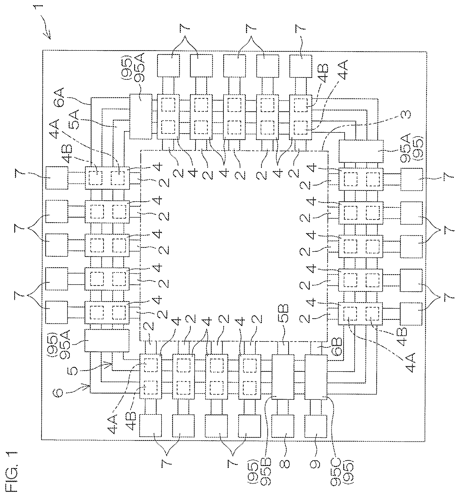
is a plan view of an IC chip 1 serving as a semiconductor device according to a preferred embodiment of the present invention. The IC chip 1 has a substantially cubic shape. The IC chip 1 includes a plurality of input-output wiring lines 2 into which a signal is input from the outside or from which a signal is output to the outside, an internal circuit 3 that is electrically connected to the input-output wiring lines 2 and that serves as a to-be-protected element, and a plurality of protection elements 4 that protect the internal circuit 3 from overvoltage based on, for example, ESD. The protection element 4 is an element, chiefly, used to protect the internal circuit 3 from ESD that is input into the input-output wiring line 2 in this preferred embodiment, and therefore the protection element 4 may be referred to as, for example, an ESD protection element. The IC chip 1 additionally includes a first power wiring line 5 to which a first power-supply voltage (for example, 5 V) is applied, a second power wiring line 6 to which a second power-supply voltage (for example, reference voltage) is applied, and a plurality of pads that are connected to the wiring lines (the input-output wiring lines 2 , the first power wiring line 5 , and the second power wiring line 6 ), respectively. For descriptive convenience, the input-output wiring line 2 , the first power wiring line 5 , and the second power wiring line 6 are each shown by a solid line in , and yet this does not mean that these members appear on a surface of the IC chip 1 . The pads include a plurality of input-output pads 7 electrically connected to the input-output wiring lines 2 , respectively, a first power pad 8 electrically connected to the first power wiring line 5 , and a second power pad 9 electrically connected to the second power wiring line 6 . A connection member (not shown), such as a bonding wire, is connected to each of the pads (each of the input-output pads 7 , the first power pad 8 , and the second power pad 9 ). The first power wiring line 5 includes a first annular power wiring line 5 A that extends in a substantially annular shape such that the first annular power wiring line 5 A surrounds the internal circuit 3 and a first connection wiring line 5 B that is electrically connected to the first annular power wiring line 5 A, to the first power pad 8 , and to the internal circuit 3 in a plan view. The second power wiring line 6 includes a second annular power wiring line 6 A that extends in a substantially annular shape such that the second annular power wiring line 6 A surrounds the internal circuit 3 outside the first power wiring line 5 and a second connection wiring line 6 B that is electrically connected to the second annular power wiring line 6 A, to the second power pad 9 , and to the internal circuit 3 in a plan view. Each of the protection elements 4 is disposed at a position coinciding with the first annular power wiring line 5 A of the first power wiring line 5 and with the second annular power wiring line 6 A of the second power wiring line 6 in a plan view. Each of the protection elements 4 includes a plurality of first protection elements 4 A that are electrically connected to the first power wiring line 5 and to the input-output wiring line 2 and a second protection element 4 B that is electrically connected to the second power wiring line 6 and to the input-output wiring line 2 . In each of the protection elements 4 , the first protection element 4 A is disposed at a position coinciding with the first annular power wiring line 5 A of the first power wiring line 5 in a plan view, and the second protection element 4 B is disposed at a position coinciding with the second annular power wiring line 6 A of the second power wiring line 6 in a plan view. The IC chip 1 additionally includes a large-capacity protection element 95 that has an electrostatic capacity larger than the protection element 4 . The large-capacity protection element 95 is composed of, for example, a NMOS (Negative-channel Metal Oxide Semiconductor) type transistor and a diode. In this preferred embodiment, the large-capacity protection element 95 is provided as a plurality of large-capacity protection elements. The large-capacity protection elements 95 are disposed at positions coinciding with the first annular power wiring line 5 A of the first power wiring line 5 and the second annular power wiring line 6 A of the second power wiring line 6 , respectively, in a plan view. The large-capacity protection elements 95 include a plurality of first large-capacity protection elements 95 A disposed at positions not coinciding with the first connection wiring line 5 B and the second connection wiring line 6 B, respectively, in a plan view, a second large-capacity protection element 95 B disposed at a position coinciding with the first connection wiring line 5 B of the first power wiring line 5 in a plan view, and a third large-capacity protection element 95 C disposed at a position coinciding with the second connection wiring line 6 B of the second power wiring line 6 in a plan view. is a plan view of the protection element 4 and of an area surrounding the protection element 4 . In , a first contact electrode 67 A, a second contact electrode 72 A, a third contact electrode 67 B, a fourth contact electrode 72 B, a first connection structure 65 A, a second connection structure 70 A, a third connection structure 65 B, a fourth connection structure 70 B, a first interlayer insulating film 60 A, and a second interlayer insulating film 60 B, which are described later, are removed. The protection element 4 has a semiconductor layer 10 and a region defining structure 15 that defines a first active region 8 A in which the first protection element 4 A is formed and a second active region 8 B in which the second protection element 4 B is formed. The semiconductor layer 10 is made of, for example, an Si monocrystal. The semiconductor layer 10 has a first principal surface 11 on one side and a second principal surface 12 on the other side (see and described later). The region defining structure 15 includes a first element separation portion 16 A that has an endless shape in a plan view and that surrounds the first active region 8 A and a second element separation portion 16 B that has an endless shape in a plan view and that surrounds the second active region 8 B. In the present preferred embodiment, the first element separation portion 16 A and the second element separation portion 16 B are each formed in a quadrangular annular shape in a plan view seen from the normal direction Z of the first and second principal surfaces 11 and 12 (also see ) (hereinafter, referred to simply as a “plan view”). The first active region 8 A and the second active region 8 B are each defined in a quadrangular shape by means of the region defining structure 15 in a plan view. The first element separation portion 16 A and the second element separation portion 16 B of the region defining structure 15 are integrally formed between the first active region 8 A and the second active region 8 B in an example shown in . The thus integrally formed first element separation portion 16 A and second element separation portion 16 B are formed as a separation portion 17 that separates the first active region 8 A and the second active region 8 B from each other. In a case in which the first element separation portion 16 A and the second element separation portion 16 B are formed with an interval therebetween unlike the example of , the separation portion 17 of the region defining structure 15 consists of the first element separation portion 16 A and the second element separation portion 16 B that face each other across a region of a part of the semiconductor layer 10 . A direction in which a side of the first element separation portion 16 A extends in a plan view is defined as a first direction X. A direction perpendicular to both the first direction X and the normal direction Z is defined as a second direction Y. In this preferred embodiment, the first active region 8 A and the second active region 8 B face each other with respect to the first direction X. The region defining structure 15 includes a trench 18 formed by digging the first principal surface 11 down toward the second principal surface 12 and an insulating embedded object 19 embedded in the trench 18 . An insulator forming the insulating embedded object 19 is optional. The insulating embedded object 19 may include at least one of silicon oxide (SiO 2 ) and silicon nitride (SiN). In this preferred embodiment, the insulating embedded object 19 is made of silicon oxide. is a cross-sectional view taken along line III-III shown in . is an enlarged view of region IV shown in . is an enlarged view of region V shown in . Referring to , the semiconductor layer 10 includes an n-type first well region 20 A formed at a surface layer portion of the first principal surface 11 in the first active region 8 A. The first principal surface 11 in the first active region 8 A is also a surface of the first well region 20 A. For example, N (nitrogen), P (phosphorus), As (arsenic), Sb (antimony), or the like is used as an n-type impurity. The n-type impurity concentration of the first well region 20 A may be not less than 1.0×10 15 cm −3 and not more than 1.0×10 18 cm −3 . A thickness TW 1 of the first well region 20 A is, for example, not less than 1 μm and not more than 1.4 μm, and is, preferably, 1.4 μm. The first protection element 4 A includes a plurality of (in this preferred embodiment, six) n-type (first-conductivity-type) first n-type impurity regions 30 A (first impurity regions) formed at a surface layer portion of the surface of the first well region 20 A and a plurality of (in this preferred embodiment, six) p-type (second-conductivity-type) first p-type impurity regions 40 A (second impurity regions) formed at the surface layer portion of the surface of the first well region 20 A (also see ). In the n-type impurity regions, a plurality of regions surrounding the first p-type impurity regions 40 A are each defined as the first n-type impurity region 30 A in . Unlike an example shown in , each of the first n-type impurity regions 30 A may be separated from each other by means of, for example, an insulating film although the first n-type impurity regions 30 A are connected together and are integrally formed in . The number of the first p-type impurity regions 40 A provided here is equal to the number of the first n-type impurity regions 30 A. Referring to and , the n-type impurity concentration of each of the first n-type impurity regions 30 A is, for example, not less than 10×10 17 cm −3 and not more than 10×10 20 cm −3 . For example, N (nitrogen), P (phosphorus), As (arsenic), Sb (antimony), or the like is used as the n-type impurity. A thickness T 1 of the first n-type impurity region 30 A is, for example, 140 nm. The first n-type impurity region 30 A has a first inner wall portion 31 A having a circular shape in a plan view and a first bottom wall portion 32 A that is connected to the first inner wall portion 31 A and that is contiguous to the first well region 20 A. The first bottom wall portion 32 A includes a curved portion that protrudes to a side opposite to the first principal surface 11 of the semiconductor layer 10 and a flat portion that connects the curved portions together. Each of the first p-type impurity regions 40 A is placed inside the first inner wall portion 31 A corresponding to the first p-type impurity region 40 A. In other words, each of the first p-type impurity regions 40 A faces the first n-type impurity region 30 A corresponding thereto with an interval between the first p-type impurity region 40 A and the first n-type impurity region 30 A. Each of the first p-type impurity regions 40 A is formed in an endless annular shape. In the example of , each of the first p-type impurity regions 40 A is formed in a circular shape in a plan view. The p-type impurity concentration of each of the first p-type impurity regions 40 A is, for example, not less than 10×10 17 cm −3 and not more than 10×10 20 cm −3 . For example, B (boron), Al (aluminum), BF 2 (compound that contains boron and fluorine), or the like is used as the p-type impurity. A thickness T 2 of the first p-type impurity region 40 A is larger than the thickness T 1 of the first n-type impurity region 30 A. The thickness T 2 of each of the first p-type impurity regions 40 A is, for example, 180 nm. The first protection element 4 A includes a first intermediate insulating layer 35 A placed between the first n-type impurity region 30 A and the first p-type impurity region 40 A and a first inner insulating layer 36 A placed inside the first p-type impurity region 40 A. The first intermediate insulating layer 35 A is embedded in a first intermediate trench 37 A formed by digging the first principal surface 11 down toward the second principal surface 12 . An insulator forming the first intermediate insulating layer 35 A is optional. The first intermediate insulating layer 35 A may include at least one of silicon oxide and silicon nitride. The first inner insulating layer 36 A is embedded in a first inner trench 38 A formed by digging the first principal surface 11 down toward the second principal surface 12 . An insulator forming the first inner insulating layer 36 A is optional. The first inner insulating layer 36 A may include at least one of silicon oxide and silicon nitride. The first p-type impurity region 40 A has a first outer wall 41 A that is contiguous to the first intermediate insulating layer 35 A and that faces the first inner wall portion 31 A across the first intermediate insulating layer 35 A, a first inner wall 42 A contiguous to the first inner insulating layer 36 A, and a first bottom wall 43 A that connects the first outer wall 41 A and the first inner wall 42 A together. The first outer wall 41 A is surrounded by the first intermediate insulating layer 35 A such that the first outer wall 41 A is contiguous to the first intermediate insulating layer 35 A. The first inner wall 42 A surrounds the first inner insulating layer 36 A such that the first inner wall 42 A is contiguous to the first inner insulating layer 36 A. The first bottom wall 43 A is contiguous to the first well region 20 A. The first bottom wall 43 A includes an outer curved portion and an inner curved portion both of which protrude to a side opposite to the first principal surface 11 of the semiconductor layer 10 and a flat portion that connects the outer curved portion and the inner curved portion together. The first p-type impurity region 40 A forms a pn junction portion PJ 1 between the first well region 20 A and the first p-type impurity region 40 A. The pn junction portion PJ 1 is formed near a contact interface between the first p-type impurity region 40 A and the first well region 20 A. In detail, the pn junction portion PJ 1 is formed at a contact interface between the first bottom wall 43 A and the first well region 20 A. Referring to , the first inner wall portion 31 A of the first n-type impurity region 30 A and the first outer wall 41 A of the first p-type impurity region 40 A corresponding to this first inner wall portion 31 A of the first n-type impurity region 30 A extend in parallel with each other. A distance L 1 between the first inner wall portion 31 A of the first n-type impurity region 30 A and the first outer wall 41 A of the first p-type impurity region 40 A corresponding to this first inner wall portion 31 A of the first n-type impurity region 30 A is constant along a circumferential direction of the first inner wall portion 31 A (which is also a circumferential direction of the first outer wall 41 A). Additionally, a distance L 2 between the first inner wall 42 A and the first outer wall 41 A of the first p-type impurity region 40 A (width of the first bottom wall 43 A of the first p-type impurity region 40 A) is also constant along a circumferential direction of the first inner wall 42 A. A first diode 50 A is formed by the first well region 20 A, the first n-type impurity region 30 A, and the first p-type impurity region 40 A. In the first active region 8 A, the first diode 50 A is provided as a plurality of first diodes 50 A the number of which is equal to that of the first p-type impurity regions 40 A (see ). In the example of , the first diode 50 A is provided as six first diodes 50 A. The first protection element 4 A additionally includes a plurality of (in the example of , five) first interlayer insulating films 60 A laminated on the first principal surface 11 of the semiconductor layer 10 . The first annular power wiring line 5 A is formed on the first interlayer insulating film 60 A, which is one of the first interlayer insulating films 60 A, such that the first annular power wiring line 5 A is contiguous to the first interlayer insulating film 60 A. The input-output wiring line 2 is formed on the first interlayer insulating film 60 A differing from the first power wiring line 5 such that the input-output wiring line 2 is contiguous to this first interlayer insulating film 60 A. In the example of , the first annular power wiring line 5 A is formed on the first interlayer insulating film 60 A that is farthest from the first principal surface 11 , and the input-output wiring line 2 is formed on the first interlayer insulating film 60 A that is a third layer from the first principal surface 11 . The first n-type impurity region 30 A of the first protection element 4 A is electrically connected to the first power wiring line 5 , and the first p-type impurity region 40 A of the first protection element 4 A is electrically connected to the input-output wiring line 2 . In detail, the first protection element 4 A additionally includes the first connection structure 65 A that electrically connects the first n-type impurity region 30 A and the first annular power wiring line 5 A together and the second connection structure 70 A that electrically connects the first p-type impurity region 40 A and the input-output wiring line 2 together. The first connection structure 65 A includes a plurality of first via holes 66 A each of which passes through any one of the first interlayer insulating films 60 A, a plurality of first contact electrodes 67 A embedded in the first via holes 66 A, respectively, and a plurality of first connection wiring lines 68 A that are formed on the first interlayer insulating film 60 A and each of which connects the first contact electrodes 67 A together. The second connection structure 70 A includes a plurality of second via holes 71 A each of which passes through any one of the first interlayer insulating films 60 A, a plurality of second contact electrodes 72 A embedded in the second via holes 71 A, respectively, and a plurality of second connection wiring lines 73 A that are formed on the first interlayer insulating film 60 A and each of which connects the second contact electrodes 72 A together. The second contact electrodes 72 A formed at the first interlayer insulating film 60 A contiguous to the first principal surface 11 are placed between the first inner wall 42 A and the first outer wall 41 A in a plan view (see ). The second contact electrodes 72 A formed at the first interlayer insulating film 60 A contiguous to the first principal surface 11 are equally spaced out along the external shape (first outer wall 41 A) of the first p-type impurity region 40 A. is a cross-sectional view taken along line VI-VI shown in . is an enlarged view of region VII shown in . is an enlarged view of region VIII shown in . Referring to , the semiconductor layer 10 additionally includes a p-type second well region 20 B formed at the surface layer portion of the first principal surface 11 in the second active region 8 B. The first principal surface 11 in the second active region 8 B is also a surface of the second well region 20 B. For example, B (boron), Al (aluminum), BF 2 (compound that contains boron and fluorine), or the like is used as the p-type impurity. The p-type impurity concentration of the second well region 20 B may be not less than 1.0×10 15 cm −3 and not more than 1.0×10 18 cm −3 . A thickness TW 2 of the second well region 20 B is, for example, not less than 1 μm and not more than 1.4 μm, and is, preferably, 1.0 μm. The second protection element 4 B includes a plurality of p-type (first-conductivity-type) second p-type impurity regions 30 B (first impurity regions) formed at a surface layer portion of the surface of the second well region 20 B and a plurality of n-type (second-conductivity-type) second n-type impurity regions 40 B (second impurity regions) formed at the surface layer portion of the surface of the second well region 20 B. The number of the second n-type impurity regions 40 B provided here is equal to the number of the second p-type impurity regions 30 B (see ). In , in the p-type impurity regions, a plurality of regions surrounding the second n-type impurity regions 40 B are set as the second p-type impurity regions 30 B, respectively. Unlike the example shown in , each of the second p-type impurity regions 30 B may be separated from each other by means of, for example, an insulating film although the second p-type impurity regions 30 B are connected together and are integrally formed in . Referring to and , the p-type impurity concentration of each of the second p-type impurity regions 30 B is, for example, not less than 10×10 17 cm −3 and not more than 10×10 20 cm −3 . For example, B (boron), Al (aluminum), BF 2 (compound that contains boron and fluorine), or the like is used as the p-type impurity. A thickness T 3 of the second p-type impurity region 30 B is, for example, 180 nm. The second p-type impurity region 30 B has a second inner wall portion 31 B having a circular shape in a plan view and a second bottom wall portion 32 B that is connected to the second inner wall portion 31 B and that is contiguous to the second well region 20 B. The second bottom wall portion 32 B includes a curved portion that protrudes to a side opposite to the first principal surface 11 of the semiconductor layer 10 and a flat portion that connects the curved portions together. Each of the second n-type impurity regions 40 B is placed inside the second inner wall portion 31 B corresponding to the second n-type impurity region 40 B. In other words, each of the second n-type impurity regions 40 B faces the second p-type impurity region 30 B corresponding to the second n-type impurity region 40 B with an interval between the second n-type impurity region 40 B and the second p-type impurity region 30 B. Each of the second n-type impurity regions 40 B is formed in an endless annular shape. In the example of , each of the second n-type impurity regions 40 B is formed in a circular shape in a plan view. The p-type impurity concentration of each of the second n-type impurity regions 40 B is, for example, not less than 10×10 17 cm −3 and not more than 10×10 20 cm −3 . For example, N (nitrogen), P (phosphorus), As (arsenic), or the like is used as the n-type impurity. A thickness T 4 of the second n-type impurity region 40 B is smaller than the thickness T 3 of the second p-type impurity region 30 B. The thickness T 4 of each of the second n-type impurity regions 40 B is, for example, 140 nm. The second protection element 4 B includes a second intermediate insulating layer 35 B placed between the second p-type impurity region 30 B and the second n-type impurity region 40 B and a second inner insulating layer 36 B placed inside the second n-type impurity region 40 B. The second intermediate insulating layer 35 B is embedded in a second intermediate trench 37 B formed by digging the first principal surface 11 down toward the second principal surface 12 . An insulator forming the second intermediate insulating layer 35 B is optional. The second intermediate insulating layer 35 B may include at least one of silicon oxide and silicon nitride. The second inner insulating layer 36 B is embedded in a second inner trench 38 B formed by digging the first principal surface 11 down toward the second principal surface 12 . An insulator forming the second inner insulating layer 36 B is optional. The second inner insulating layer 36 B may include at least one of silicon oxide and silicon nitride. The second n-type impurity region 40 B has a second outer wall 41 B that is contiguous to the second intermediate insulating layer 35 B and that faces the second inner wall portion 31 B across the second intermediate insulating layer 35 B, a second inner wall 42 B contiguous to the second inner insulating layer 36 B, and a second bottom wall 43 B that connects the second outer wall 41 B and the second inner wall 42 B together. The second outer wall 41 B is surrounded by the second intermediate insulating layer 35 B such that the second outer wall 41 B is contiguous to the second intermediate insulating layer 35 B. The second inner wall 42 B surrounds the second inner insulating layer 36 B such that the second inner wall 42 B is contiguous to the second inner insulating layer 36 B. The second bottom wall 43 B is contiguous to the second well region 20 B. The second bottom wall 43 B includes an outer curved portion and an inner curved portion both of which protrude to a side opposite to the first principal surface 11 of the semiconductor layer 10 and a flat portion that connects the outer curved portion and the inner curved portion together. The second n-type impurity region 40 B forms a pn junction portion PJ 2 between the second well region 20 B and the second n-type impurity region 40 B. The pn junction portion PJ 2 is formed near a contact interface between the second n-type impurity region 40 B and the second well region 20 B. In detail, the pn junction portion PJ 2 is formed at a contact interface between the second bottom wall 43 B and the second well region 20 B. Referring to , the second inner wall portion 31 B of the second p-type impurity region 30 B and the second outer wall 41 B of the second n-type impurity region 40 B corresponding to the second inner wall portion 31 B of the second p-type impurity region 30 B extend in parallel with each other. A distance L 3 between the second inner wall portion 31 B of the second p-type impurity region 30 B and the second outer wall 41 B of the second n-type impurity region 40 B corresponding to the second inner wall portion 31 B of the second p-type impurity region 30 B is constant along a circumferential direction of the second inner wall portion 31 B (which is also a circumferential direction of the second outer wall 41 B). Additionally, a distance L 4 between the second inner wall 42 B and the second outer wall 41 B of the second n-type impurity region 40 B (width of the second bottom wall 43 B of the second n-type impurity region 40 B) is also constant along a circumferential direction of the second inner wall 42 B. A second diode 50 B is formed by the second well region 20 B, the second p-type impurity regions 30 B, and the second n-type impurity region 40 B. In the second active region 8 B, the second diode 50 B is provided as a plurality of second diodes 50 B the number of which is equal to that of the second n-type impurity regions 40 B (see ). In the example of , the second diode 50 B is provided as six second diodes 50 B. The second protection element 4 B additionally includes a plurality of (in the example of , five) second interlayer insulating films 60 B laminated on the first principal surface 11 of the semiconductor layer 10 . The second annular power wiring line 6 A is formed on the second interlayer insulating film 60 B, which is one of the second interlayer insulating films 60 B, such that the second annular power wiring line 6 A is contiguous to this second interlayer insulating film 60 B. The input-output wiring line 2 is formed on the second interlayer insulating film 60 B such that the input-output wiring line 2 is contiguous to this second interlayer insulating film 60 B differing from the second power wiring line 6 . In the example of , the second annular power wiring line 6 A is formed on the second interlayer insulating film 60 B farthest from the first principal surface 11 , and the input-output wiring line 2 is formed on the second interlayer insulating film 60 B that is the third layer from the first principal surface 11 . The second n-type impurity region 40 B of the second protection element 4 B is electrically connected to the input-output wiring line 2 , and the second p-type impurity region 30 B of the second protection element 4 B is electrically connected to the second power wiring line 6 . In detail, the second protection element 4 B additionally includes the third connection structure 65 B that electrically connects the second p-type impurity region 30 B and the second power wiring line 6 together and the fourth connection structure 70 B that electrically connects the second n-type impurity region 40 B and the input-output wiring line 2 together. The third connection structure 65 B includes a plurality of third via holes 66 B each of which passes through any one of the second interlayer insulating films 60 B, a plurality of third contact electrodes 67 B embedded in the third via holes 66 B, respectively, and a plurality of third connection wiring lines 68 B that are formed on the second interlayer insulating film 60 B and each of which connects the third contact electrodes 67 B together. The fourth connection structure 70 B includes a plurality of fourth via holes 71 B each of which passes through any one of the second interlayer insulating films 60 B, a plurality of fourth contact electrodes 72 B embedded in the fourth via holes 71 B, respectively, and a plurality of fourth connection wiring lines 73 B that are formed on the second interlayer insulating film 60 B and each of which connects the fourth contact electrodes 72 B together. The fourth contact electrodes 72 B formed at the second interlayer insulating film 60 B contiguous to the first principal surface 11 are placed between the second inner wall 42 B and the second outer wall 41 B in a plan view (see ). The fourth contact electrodes 72 B formed at the second interlayer insulating film 60 B contiguous to the first principal surface 11 are equally spaced out along the external shape (second outer wall 41 B) of the first p-type impurity region 40 A. is a schematic view of an electric circuit of the IC chip 1 shown in . A signal input into the input-output pad 7 is input into the internal circuit 3 through the input-output wiring line 2 . A signal output from the internal circuit 3 is output from the input-output pad 7 to the outside through the input-output wiring line 2 . There is a case in which an overvoltage based on ESD etc., is input into the input-output pad 7 . The electric potential of the input-output pad 7 increases if the overvoltage input into the input-output pad 7 is a positive overvoltage. Hence, the first protection element 4 A operates in a forward direction, and an ESD current flows through the first power wiring line 5 . As a result, the internal circuit 3 is protected from the positive overvoltage. If the overvoltage input into the input-output pad 7 is a negative overvoltage, an electric potential between the input-output pad 7 and the second power pad 9 decreases, and hence the second protection element 4 B operates in the forward direction, and an ESD current flows through the second power wiring line 6 . As a result, the internal circuit 3 is protected from the negative overvoltage. A is a schematic view shown to describe an aspect in which electric charge has been accumulated in the first diode 50 A of the first protection element 4 A. The first well region 20 A and the first p-type impurity region 40 A form the pn junction portion PJ 1 (see ), and therefore electric charge E 1 is accumulated near an interface between the first bottom wall 43 A of the first p-type impurity region 40 A and the first well region 20 A. Here, unlike this preferred embodiment, let it be supposed that a diode 100 of a first reference example is provided in which the shape of a p-type impurity region 103 placed inside an n-type impurity region 102 is, for example, circular in a plan view, not annular, in a surface layer portion of a principal surface of a well region 101 as shown in A . In the first diode 50 A according to the preferred embodiment shown in A , the first p-type impurity region 40 has a circular shape in a plan view, hence making it possible to make the area of an interface between the first p-type impurity region 40 A and the first well region 20 A smaller when compared to the diode 100 of the first reference example shown in A . Therefore, the electric charge E 1 (see A ) accumulated near the interface between the first p-type impurity region 40 A and the first well region 20 A is smaller than electric charge E 01 (see A ) accumulated near an interface between the p-type impurity region 103 and the well region 101 of the diode 100 of the first reference example. Therefore, the electrostatic capacity of the first diode 50 A is smaller than the electrostatic capacity of the diode 100 of the first reference example. Particularly if the thickness T 2 of the first p-type impurity region 40 A is smaller than a width W 1 of the first p-type impurity region 40 A in a plan view, it is possible to reduce an amount of increase in area of the interface between the first p-type impurity region 40 A and the first well region 20 A. Therefore, the electrostatic capacity is enabled to be further reduced. If the first p-type impurity region 40 A has a circular shape in a plan view, the width W 1 of the first p-type impurity region 40 A is an outer diameter of the first p-type impurity region 40 A. B is a schematic view shown to describe an aspect in which an ESD current flows through the first diode 50 A. An ESD current C 1 flows through a part, which is contiguous to the first well region 20 A, of the first p-type impurity region 40 A. The ESD current C 1 is predominant in a part, which is close to the first n-type impurity region 30 A, of the first p-type impurity region 40 A. In detail, a contribution to an ESD current capability of a part, which is far from the first n-type impurity region 30 A, of the first p-type impurity region 40 A is much smaller than a contribution to an ESD current capability of the part, which is close to the first n-type impurity region 30 A, of the first p-type impurity region 40 A. In other words, the amount of current of the part, which is far from the first n-type impurity region 30 A, of the first p-type impurity region 40 A is smaller than the amount of current of the part, which is close to the first n-type impurity region 30 A, of the first p-type impurity region 40 . Therefore, if the first p-type impurity region 40 A has an annular shape in a plan view as shown in B , it is possible to maintain contact between the part, which is close to the first n-type impurity region 30 A, of the first p-type impurity region 40 A and the first well region 20 A, hence making it possible to improve the ESD current C 1 per capacity, i.e., improve efficiency. Therefore, it is possible to secure an ESD current capability equivalent to a configuration in which the p-type impurity region 103 shown in B has a circular shape in a plan view. Therefore, it is possible to sufficiently secure an ESD current capability even if the first p-type impurity region 40 A has an annular shape. In other words, it is possible to restrain a decrease in ESD resistance properties. Additionally, in the diode 100 of the first reference example shown in B , a contact interface between a part which is close to the center of the p-type impurity region 103 whose shape is circular in a plan view and the well region 101 hardly affects the ESD resistance properties. As thus described, it is possible to restrain a decrease in the ESD tolerance and to reduce the electrostatic capacity if the first p-type impurity region 40 is annular. A is a schematic view shown to describe an aspect in which electric charge has been accumulated in the second diode 50 of the second protection element 4 B. The second well region 20 B and the second n-type impurity region 40 B form the pn junction portion PJ 2 (see ), and therefore electric charge E 2 is accumulated near an interface between the second bottom wall 43 B of the second n-type impurity region 40 B and the second well region 20 B. Here, unlike this preferred embodiment, let it be supposed that a diode 200 of a second reference example is provided in which the shape of an n-type impurity region 203 placed inside a p-type impurity region 202 is, for example, circular in a plan view, not annular, in a surface layer portion of a principal surface of a well region 201 as shown in A . In the second diode 50 B according to the preferred embodiment shown in A , the second n-type impurity region 40 B has a circular shape in a plan view, hence making it possible to make the area of an interface between the second n-type impurity region 40 B and the second well region 20 B smaller when compared to the diode 200 of the second reference example shown in A . Therefore, the electric charge E 2 (see A ) accumulated near the interface between the second n-type impurity region 40 B and the second well region 20 B is smaller than electric charge E 02 (see A ) accumulated near an interface between the n-type impurity region 203 and the well region 201 of the diode 200 of the second reference example. Therefore, the electrostatic capacity of the second diode 50 B is smaller than the electrostatic capacity of the diode 200 of the second reference example. Particularly if the thickness T 4 of the second n-type impurity region 40 B is smaller than a width W 2 of the second n-type impurity region 40 B in a plan view, it is possible to reduce an amount of increase in area of the interface between the second n-type impurity region 40 B and the second well region 20 B. Therefore, the electrostatic capacity is enabled to be further reduced. If the second n-type impurity region 40 B has a circular shape in a plan view, the width W 2 of the second n-type impurity region 40 B is an outer diameter of the second n-type impurity region 40 B. B is a schematic view shown to describe an aspect in which an ESD current flows through the second diode 50 B. An ESD current C 2 is predominant in a part, which is close to the second p-type impurity region 30 B, of the second n-type impurity region 40 B in the same way as the ESD current C 1 of B . Therefore, if the second n-type impurity region 40 B has an annular shape in a plan view as shown in B , it is possible to maintain contact between the part, which is close to the second p-type impurity region 30 B, of the second n-type impurity region 40 B and the second well region 20 B, hence making it possible to improve the ESD current C 2 per capacity, i.e., improve efficiency. Therefore, it is possible to secure an ESD current capability equivalent to a configuration in which the n-type impurity region 203 shown in B has a circular shape in a plan view. Therefore, it is possible to sufficiently secure an ESD current capability even if the second n-type impurity region 40 B has an annular shape. In other words, it is possible to restrain a decrease in ESD resistance properties. Additionally, in the diode 200 of the second reference example shown in B , a contact interface between a part which is close to the center of the n-type impurity region 203 whose shape is circular in a plan view and the well region 201 hardly affects the ESD resistance properties. As thus described, it is possible to restrain a decrease in the ESD tolerance and to reduce the electrostatic capacity if the second n-type impurity region 40 B is annular. With this preferred embodiment, the first p-type impurity region 40 A and the second n-type impurity region 40 B are annular, hence making it possible to reduce the charge amount of both the first p-type impurity region 40 A and the second n-type impurity region 40 B that are connected to the input-output wiring line 2 . Therefore, it is possible to improve the speed of an electric signal input into the internal circuit 3 . Next, first to fifth modifications of the diodes 50 A and 50 B of the protection element 4 according to this preferred embodiment will be described. is a plan view of the first diode 50 A of the first modification. In the first diode 50 A of the first modification, the first p-type impurity region 40 A has an ended circular shape unlike the first diode 50 A shown in . The first p-type impurity region 40 A has the shape of, for example, the capital letter C. The first p-type impurity region 40 A has an ended circular shape, and therefore the first intermediate insulating layer 35 A and the first inner insulating layer 36 A are connected together by means of a connection insulating layer 39 A. If the first p-type impurity region 40 A has an ended circular shape in a plan view, the width W 1 of the first p-type impurity region 40 A is an outer diameter of the first p-type impurity region 40 A. In the second diode 50 B, the same modification can be applied (not shown). In detail, the second n-type impurity region 40 B may have an ended circular shape (for example, the capital letter C). In this case, the second intermediate insulating layer 35 B and the second inner insulating layer 36 B are connected together by means of a connection insulating layer. is a plan view of the first diode 50 A of the second modification. is a plan view of the first diode 50 A of the third modification. is a plan view of the first diode 50 A of the fourth modification. The first p-type impurity region 40 A may be polygonal annular shape in a plan view as shown in to . In detail, the first p-type impurity region 40 A may be octagonal annular as shown in , or may be hexagonal annular as shown in , or may be quadrangular annular as shown in . The first p-type impurity region 40 A may have a polygonal annular shape other than an octagonal annular shape, a hexagonal annular shape, and a quadrangular annular shape, and may have, for example, a triangular annular shape. In the first diode 50 A of the second to fourth modifications, the first p-type impurity region 40 A has an endless annular shape in a plan view surrounding the first inner insulating layer 36 A. There is a concern that the ESD current will concentrate on a corner portion 40 a of the first p-type impurity region 40 A if the first p-type impurity region 40 A is polygonal annular shape in a plan view and if the second contact electrodes 72 A formed at the first interlayer insulating film 60 A contiguous to the first principal surface 11 are disposed on the corner portion 40 a of the first p-type impurity region 40 A. Therefore, in the first diode 50 A of the second to fourth modifications, the second contact electrodes 72 A are disposed along an external shape 40 b of the first p-type impurity region 40 A such that the second contact electrodes 72 A avoid the corner portion 40 a of the first p-type impurity region 40 A in a plan view. This makes it possible to restrain the concentration of the ESD current in the corner portion 40 a of the first p-type impurity region 40 A. In the first diode 50 A of the second to fourth modifications, the width W 1 of the first p-type impurity region 40 A is a distance between a pair of sides that extend in parallel with each other in the external shape of the first p-type impurity region 40 A. Likewise, in the second diode 50 B, the same modification can be applied (not shown). In detail, the second n-type impurity region 40 B may be polygonal annular shape in a plan view. The present invention can be embodied in still other modes. For example, the first p-type impurity region 40 A may have an ended shape even if the first p-type impurity region 40 A is polygonal annular shape in a plan view like the first diode 50 A of the second to fourth modifications. The same applies to each of the modifications of the second diode 50 B. In other words, the second n-type impurity region 40 B may have an ended shape even if the second n-type impurity region 40 B is polygonal annular shape in a plan view. The IC chip 1 according to the aforementioned preferred embodiment can be used in an IC that deals with a comparatively large electric current, such as a power IC or an IC (motor driver) that controllably drives a motor, and can be used in electric apparatuses that use this IC. Additionally, the semiconductor device according to the present invention can be applied to various electric apparatuses, i.e., can be applied to mobile telecommunications products, such as a mobile phone and PHS (Personal Handyphone System), and pieces of information processing equipment typified by personal computers. The operation of these electric apparatuses is controlled by the IC chip 1 according to the aforementioned preferred embodiment. Additionally, unlike the aforementioned preferred embodiment, the protection element 4 can be used as, for example, a protection element that protects MOSFET (Metal Oxide Semiconductor Field Effect Transistor) without being limited to a protection element that protects an internal circuit of an IC chip. In the aforementioned preferred embodiment, each of the protection elements 4 A and 4 B is formed by the diodes 50 A and 50 B. However, each of the protection elements 4 A and 4 B may be formed by the single diode 50 A or 50 B. Examples of features extracted from this description and from the drawings will be hereinafter shown. [A1] to [A14] mentioned below provide a semiconductor device whose barrier height has been reduced. [A1] A semiconductor device including a semiconductor layer having a principal surface, a first-conductivity-type well region formed at a surface layer portion of the principal surface of the semiconductor layer, a first-conductivity-type first impurity region that is formed at a surface layer portion of the well region and that has an inner wall portion, and a second-conductivity-type annular second impurity region formed at the surface layer portion of the well region on a more inward side than the inner wall portion such that a pn junction portion is formed between the well region and the second impurity region. With this arrangement, the well region and the second impurity region form a pn junction portion, and therefore electric charge is accumulated near an interface between the second impurity region and the well region. With the aforementioned arrangement, the second impurity region is annular. Therefore, it is possible to make the area of the interface between the second impurity region and the well region smaller when compared to an arrangement in which the shape of the second impurity region is, for example, circular, not annular, in a plan view unlike the aforementioned arrangement. Therefore, it is possible to reduce an electrostatic capacity. Additionally, if the second impurity region is annular, it is possible to secure an ESD current capability equivalent to an arrangement in which the shape of the second impurity region in a plan view is a circular shape. Therefore, it is possible to restrain a decrease in ESD current capability. In other words, it is possible to restrain a decrease in ESD resistance properties. As thus described, it is possible to restrain a decrease in ESD tolerance and to reduce the electrostatic capacity if the second impurity region is annular. [A2] The semiconductor device according to A1, wherein the second impurity region has an outer wall that faces the inner wall portion, an inner wall that is contiguous to the well region, and a bottom wall that connects the outer wall and the inner wall together. [A3] The semiconductor device according to A2, wherein the first impurity region has a bottom wall portion that is connected to the inner wall portion and that is contiguous to the well region, and the bottom wall portion of the first impurity region is placed on a side of the principal surface of the semiconductor layer with respect to the bottom wall of the second impurity region. [A4] The semiconductor device according to A2 or A3, further including an intermediate insulating layer that is placed between the first impurity region and the second impurity region and that is contiguous to the outer wall. [A5] The semiconductor device according to any one of A2 to A4, further including an inner insulating layer that is placed inside the second impurity region and that is contiguous to the inner wall. [A6] The semiconductor device according to any one of A1 to A5, wherein a thickness of the second impurity region is smaller than a width of the second impurity region in a plan view. [A7] The semiconductor device according to any one of A1 to A6, wherein the second impurity region is circular in a plan view. [A8] The semiconductor device according to any one of A1 to A5, wherein the second impurity region is polygonal annular shape in a plan view. [A9] The semiconductor device according to A8, further including an insulating film that is formed on the semiconductor layer and in which a plurality of via holes are formed, and a plurality of contact electrodes that are formed in the via holes, respectively, and that are connected to the second impurity region, wherein the contact electrodes are disposed along an external shape of the second impurity region such that the contact electrodes avoid a corner portion of the second impurity region in a plan view. [A10] The semiconductor device according to any one of A1 to A9, wherein the first impurity region is endless in a plan view. [A11] The semiconductor device according to any one of A1 to A10, further including a plurality of diodes formed by the well region, the first impurity region, and the second impurity region; and a region defining structure that defines an active region in which the diodes are formed. [A12] The semiconductor device according to A11, wherein the first impurity region of the diodes is integrally formed. [A13] The semiconductor device according to A11 or A12, further including an input-output wiring line into which or from which a signal is input or is output; a to-be-protected element that is connected to the input-output wiring line; and a protection element that is formed by the diode and that protects the to-be-protected element from an overvoltage applied to the input-output wiring line. [A14] The semiconductor device according to A13, further including a first power wiring line to which a first power-supply voltage is applied; and a second power wiring line to which a second power-supply voltage lower than the first power-supply voltage is applied; wherein the protection element includes a first protection element in which the first impurity region is electrically connected to the first power wiring line and in which the second impurity region is electrically connected to the input-output wiring line, and a second protection element in which the first impurity region is electrically connected to the second power wiring line and in which the second impurity region is electrically connected to the input-output wiring line. Although the preferred embodiments of the present invention have been described in detail, these preferred embodiments are merely specific examples used to clarify the technical contents of the present invention, and the present invention should not be interpreted as being limited to these specific examples, and the scope of the present invention shall be limited solely by the appended claims. This application corresponds to Japanese Patent Application No. 2020-215445 filed with the Japan Patent Office on Dec. 24, 2020, the entire disclosure of which is incorporated herein by reference. REFERENCE SIGNS LIST 1 : IC chip (semiconductor device) 2 : Input-output wiring line 3 : Internal circuit (to-be-protected element) 4 : Protection element 4 A: First protection element 4 B: Second protection element 5 : First power wiring line 6 : Second power wiring line 8 A: First active region 8 B: Second active region 10 : Semiconductor layer 11 : First principal surface 15 : Region defining structure 30 A: First n-type impurity region (First impurity region) 30 B: Second p-type impurity region (First impurity region) 31 A: First inner wall portion 31 B: Second inner wall portion 32 A: First bottom wall portion 32 B: Second bottom wall portion 40 A: First p-type impurity region (Second impurity region) 40 B: Second n-type impurity region (Second impurity region) 41 A: First outer wall 41 B: Second outer wall 42 A: First inner wall 42 B: Second inner wall 43 A: First bottom wall 43 B: Second bottom wall 50 A: First diode 50 B: Second diode 60 A: First interlayer insulating film 60 B: Second interlayer insulating film 71 A: Second via hole 71 B: Fourth via hole 72 A: Second contact electrode 72 B: Fourth contact electrode PJ 1 : Pn junction portion PJ 2 : Pn junction portion T 2 : Thickness T 4 : Thickness
Figures (20)
Citations
This patent cites (15)
- US6590264
- US7012304
- US8143690
- US9559170
- US10157903
- US11302686
- US11742342
- US2007/0278614
- US2009/0261418
- US2013/0020673
- US2018/0294364
- USH07169980
- US2012-049444
- US2013-026384
- US2017-073594