Stress Absorbing Trench Capacitor and Method for Forming the Same
Abstract
The present disclosure provides a method of manufacturing a semiconductor structure. The method includes providing a substrate; forming a trench with a predetermined aspect ratio in the substrate to form two fins, wherein the forming of the trench induces the substrate to warp toward a first direction; forming a metal-insulator-metal (MIM) stack on sidewalls of the two fins in the trench, and leaving a space surrounded by the MIM stack in the trench; determining whether the substrate warps toward a second direction reverse to the first direction after the forming of the MIM stack; and in response to the substrate warping toward the second direction, depositing an insulating layer to cover an upper surface of the MIM stack and seal the trench to thereby leave a void in the space.
Claims (20)
1 . A method of manufacturing a semiconductor structure, comprising: providing a substrate; forming a trench with a predetermined aspect ratio in the substrate to form two fins, wherein the forming of the trench induces the substrate to warp toward a first direction; forming a liner layer to cover the substrate and the two fins, wherein the liner layer has different widths at different heights of the two fins, resulting in sidewalls of the liner layer within the trench being parallel to each other; forming a metal-insulator-metal (MIM) stack on the sidewalls of the liner layer that are on the two fins in the trench, and leaving a space surrounded by the MIM stack in the trench; determining whether the substrate warps toward a second direction reverse to the first direction after the forming of the MIM stack; and depositing an insulating layer to cover an upper surface of the MIM stack and seal the trench, thereby leaving a void in the space, wherein an amount of the insulating layer is associated with a warpage level of the substrate.
10 . A method of manufacturing a semiconductor structure, comprising: providing a substrate; forming two fins separated by etching a trench with a predetermined aspect ratio in the substrate; forming a liner layer to cover the substrate and the two fins, wherein the liner layer has different widths at different heights of the two fins, resulting in sidewalls of the liner layer within the trench being parallel to each other on the two fins; forming a capacitor on the sidewalls of the liner layer that are on the two fins, and leaving a space surrounded by the capacitor between the two fins; determining a warpage level of the substrate; and depositing an insulating layer over the capacitor and the trench to seal the space and leave a void in the trench, wherein a thickness of the insulating layer in the trench is associated with the warpage level of the substrate.
16 . A semiconductor structure, comprising: a substrate; two fins separated to each other by a trench in the substrate; a liner layer continuously on the substrate and the two fins, wherein the liner layer has different widths at different heights of the two fins, resulting in sidewalls of the liner layer within the trench being parallel to each other; a first conductive layer on the liner layer over the substrate and sidewalls of the two fins; a dielectric layer on the first conductive layer; a second conductive layer on the dielectric layer; and an insulating layer covering a top portion and sidewalls of the second conductive layer in the trench, wherein the insulating layer includes a void within the insulating layer, wherein the void has a first width proximal to adjacent upper corners of the two fins less than a second width proximal to a bottom of the fins.
Show 17 dependent claims
2 . The method of claim 1 , wherein the predetermined aspect ratio ranges from about 20:1 to about 140:1.
3 . The method of claim 1 , wherein the void tapers from a bottom of the trench toward an entrance of the trench.
4 . The method of claim 1 , wherein the insulating layer is formed by plasma-enhanced CVD (PECVD), and a flow rate of gas precursors of the insulating layer is greater than 10 sccm.
5 . The method of claim 1 , wherein the forming of the MIM stack includes: depositing a first conductive layer on the liner layer; depositing a dielectric layer on the first conductive layer; and depositing a second conductive layer on the dielectric layer to thereby keep the trench open with a substantially equal width across a height of the trench.
6 . The method of claim 5 , wherein each of the first conductive layer, the dielectric layer and the second conductive layer is deposited using an ALD operation.
7 . The method of claim 5 , wherein each of the first conductive layer, the dielectric layer and the second conductive layer grows at a first deposition rate slower than a second deposition rate of the insulating layer.
8 . The method of claim 7 , wherein the first deposition rate keeps substantially constant during the forming of the MIM stack, and the second deposition rate decreases from the bottom of the trench toward the entrance of the trench.
9 . The method of claim 7 , wherein the second deposition rate of the insulating layer outside the trench is greater than the second deposition rate of the insulating layer inside the trench.
11 . The method of claim 10 , wherein the forming of the capacitor comprising depositing an MIM stack includes depositing a dielectric layer sandwiched between a pair of conductive layers, wherein the dielectric layer is made of a high dielectric constant (high k) material including HfO 2 , Ta 2 O 5 , AlO, SIN, SiNO, Al 2 O 3 , TiO 2 , ZrO 2 , La 2 O 3 or Pr 2 O 3 and has a thickness less than 100 angstroms (Å), the pair of conductive layers is made of polysilicon or metals and each of the pair of conductive layers has a thickness between about 200 Å and about 300 Å, and the insulating layer is made of an antireflective material, undoped silicon glass, or oxide.
12 . The method of claim 10 , wherein the insulating layer is deposited to an amount over the capacitor such that the insulating layer over adjacent upper corners of the two fins is thick enough to contact each other to completely cover the space, and the insulating layer is nonuniformly coated on an inner sidewall of the trench.
13 . The method of claim 12 , wherein when the space is sealed, the void has a first width proximal to the adjacent upper corners of the two fins less than a second width proximal to a bottom of the trench, and a height of the void is equal to or more than 95% of a depth of the trench.
14 . The method of claim 12 , wherein when the space is sealed, a distance between a bottommost point of the void and a bottommost point of the trench is in a range of about 80 nanometers (nm) to about 120 nm.
15 . The method of claim 12 , wherein when the space is sealed, the insulating layer covering an upper portion of the capacitor in a top half of the trench accumulates to a first thickness, and the insulating layer covering a lower portion of the capacitor in a bottom half of the trench accumulates to a second thickness, where in a thickness ratio between the first thickness and the second thickness is about 1.5 to about 5.5.
17 . The semiconductor structure of claim 16 , wherein the height of each one of the two fins is between about 3 micrometers (μm) and about 15 μm.
18 . The semiconductor structure of claim 17 , wherein the void tapers from the bottom of the fins toward the adjacent upper corners of the two fins, and the height of the void is equal to or more than 95% of the height of each one of the two fins.
19 . The semiconductor structure of claim 17 , wherein the insulating layer has a first thickness that is proximal to the adjacent upper corners of the two fins and greater than a second thickness that is proximal to the bottom of the fins, and wherein the first thickness decreases to the second thickness in a direction toward the bottom of the fins.
20 . The semiconductor structure of claim 19 , wherein the first thickness is between about 15 nm and about 22 nm and the second thickness is between about 4 nm and about 10 nm.
Full Description
Show full text →
PRIORITY
CLAIM
AND
CROSS-REFERENCE
This application claims priority to U.S. Provisional Application No. 63/220,433 filed Jul. 9, 2021, the disclosures of which are hereby incorporated by reference in its entirety.
BACKGROUND
A basic capacitor is a device including a dielectric layer sandwiched by a pair of electrodes. A capacitor may be employed as a charge storage unit in a dynamic random access memory (DRAM), may be provided as a stand-alone semiconductor chip, or may be embedded in a system-on-chip (SoC) semiconductor chip. In addition, a capacitor may also be employed in a variety of circuit applications such as a charge pump or a capacitive analog component in a radio-frequency (RF) circuit.
BRIEF DESCRIPTION OF THE DRAWINGS
Aspects of the embodiments of the present disclosure are best understood from the following detailed description when read with the accompanying figures. It should be noted that, in accordance with the standard practice in the industry, various structures are not drawn to scale. In fact, the dimensions of the various structures can be arbitrarily increased or reduced for clarity of discussion. A is a schematic cross-sectional view of a semiconductor device, in accordance with some embodiments of the present disclosure. B is an enlarged view showing a void in the semiconductor device in A , in accordance with some embodiments of the present disclosure. is a flow diagram showing a method of fabricating a semiconductor device, in accordance with some embodiments of the present disclosure. , 4 A to 4 G, 7 to 13 , 15 A to 15 D and 16 to 21 are schematic cross-sectional views illustrating sequential operations of the method shown in , in accordance with some embodiments of the present disclosure. is a schematic top view of C or 4 G , in accordance with some embodiments of the present disclosure. is a schematic side view of a substrate including multiple trenches, in accordance with some embodiments of the present disclosure. is a schematic side view of a substrate including multiple MIM capacitors, in accordance with some embodiments of the present disclosure. is a schematic cross-sectional view showing an interconnect structure formed over the semiconductor device in A . is a schematic cross-sectional view showing a semiconductor structure including the semiconductor device in A and the interconnect structure in .
DETAILED DESCRIPTION
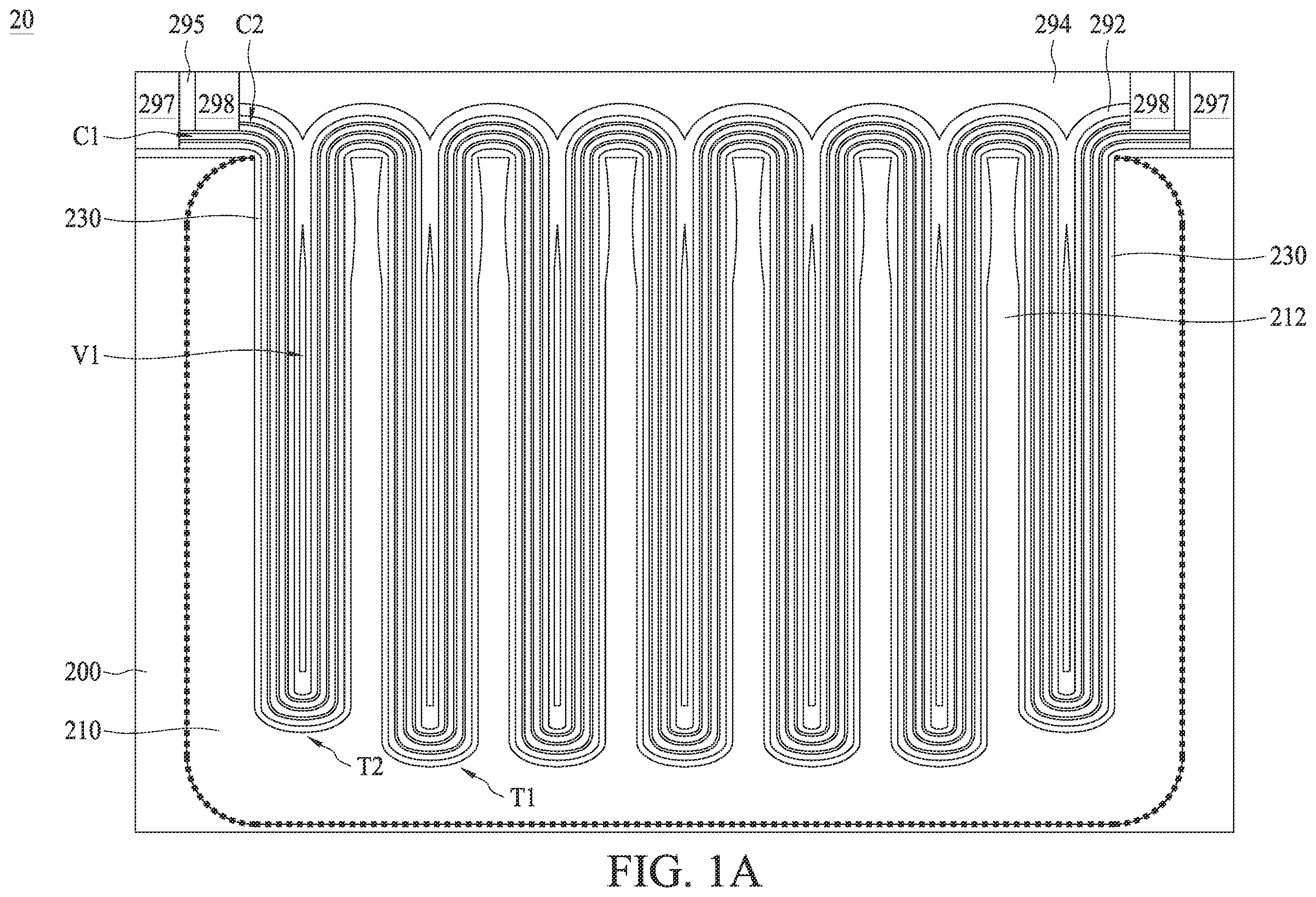
The following disclosure provides many different embodiments, or examples, for implementing different features of the provided subject matter. Specific examples of elements and arrangements are described below to simplify the present disclosure. These are, of course, merely examples and are not intended to be limiting. For example, the formation of a first feature over or on a second feature in the description that follows may include embodiments in which the first and second features are formed in direct contact, and may also include embodiments in which additional features can be formed between the first and second features, such that the first and second features may not be in direct contact. In addition, the present disclosure may repeat reference numerals and/or letters in the various examples. This repetition is for the purpose of simplicity and clarity and does not in itself dictate a relationship between the various embodiments and/or configurations discussed. Further, spatially relative terms, such as “beneath,” “below,” “lower,” “above,” “over,” “upper,” “on” and the like, can be used herein for ease of description to describe one element or feature's relationship to another element(s) or feature(s) as illustrated in the figures. The spatially relative terms are intended to encompass different orientations of the device in use or operation in addition to the orientation depicted in the figures. The apparatus can be otherwise oriented (rotated 90 degrees or at other orientations) and the spatially relative descriptors used herein may likewise be interpreted accordingly. As used herein, although terms such as “first,” “second” and “third” describe various elements, components, regions, layers and/or sections, these elements, components, regions, layers and/or sections should not be limited by these terms. These terms may only be used to distinguish one element, component, region, layer or section from another. Terms such as “first,” “second” and “third” when used herein do not imply a sequence or order unless clearly indicated by the context. Notwithstanding that the numerical ranges and parameters setting forth the broad scope of the disclosure are approximations, the numerical values set forth in the specific examples are reported as precisely as possible. Any numerical value, however, inherently contains certain errors necessarily resulting from the standard deviation found in the respective testing measurements. Also, as used herein, the terms “substantially,” “approximately” and “about” generally mean within a value or range that can be contemplated by people having ordinary skill in the art. Alternatively, the terms “substantially,” “approximately” and “about” mean within an acceptable standard error of the mean when considered by one of ordinary skill in the art. People having ordinary skill in the art can understand that the acceptable standard error may vary according to different technologies. Other than in the operating/working examples, or unless otherwise expressly specified, all of the numerical ranges, amounts, values and percentages such as those for quantities of materials, durations of times, temperatures, operating conditions, ratios of amounts, and the likes thereof disclosed herein should be understood as modified in all instances by the terms “substantially,” “approximately” or “about.” Accordingly, unless indicated to the contrary, the numerical parameters set forth in the present disclosure and attached claims are approximations that can vary as desired. At the very least, each numerical parameter should at least be construed in light of the number of reported significant digits and by applying ordinary rounding techniques. Ranges can be expressed herein as from one endpoint to another endpoint or between two endpoints. All ranges disclosed herein are inclusive of the endpoints, unless specified otherwise. A basic trench capacitor is a small three-dimensional device formed by etching a trench into a semiconductor substrate. A deep trench capacitor (DTC) is used to provide capacitance to various integrated circuits (ICs). Deep trench capacitors can be used in a variety of semiconductor chips for high areal capacitance and low device leakage. Typically, a deep trench capacitor provides a capacitance in the range from 4 femtoFarad (fF) to 120 fF. An advantage of using the deep trench capacitor over package structures is that it can be freely placed as close as possible to the desired processing units. Additionally, the deep trench capacitor can also provide higher capacitance per unit area. Deep trench capacitors are commonly embedded in integrated passive devices (IPDs) and used in place of ceramic capacitors to reduce the size of semiconductor device, reduce the cost of semiconductor devices, increase the functionality of semiconductor devices, or any combination of the foregoing. A is a schematic cross-sectional view of a semiconductor device 20 . The semiconductor device 20 includes a substrate 200 in which a doped region 210 is formed. Multiple trenches T 1 , T 2 and multiple fins 212 are formed within the doped region 210 . Each of the trenches T 1 separates adjacent fins 212 and the trench T 2 separates a fin 212 adjacent to the unpatterned substrate 200 . Each of the fins 212 may be conductive due to its containing of conductive ions or dopants. A liner layer 230 is conformally disposed on surfaces of the fins 122 . A first metal-insulator-metal (MIM) capacitor C 1 is disposed in the trenches T 1 , T 2 and conformally over the liner layer 230 . A second MIM capacitor C 2 is disposed in the trenches T 1 , T 2 and conformally over the first MIM capacitor C 1 . The second MIM capacitor C 2 is disposed in parallel to and vertically over the first MIM capacitor C 1 . The first MIM capacitor C 1 and the second MIM capacitor C 2 extend over the doped region 210 and the substrate 200 . An insulating layer 292 is disposed in the trenches T 1 , T 2 and over the second MIM capacitor C 2 . The insulating layer 292 seals the trenches T 1 and T 2 . The portion of the insulating layer 292 in the respective trenches T 1 and T 2 is substantially hollow. Multiple voids V 1 are formed inside the insulating layer 292 . An interlayer dielectric (ILD) layer 294 is disposed over the insulating layer 292 . A conductive via 297 is disposed adjacent to and electrically coupled to the first MIM capacitor C 1 . A conductive via 298 is disposed adjacent to and electrically coupled to the second MIM capacitor C 2 . The conductive via 297 and the conductive via 298 are separated by an isolation layer 295 . B is an enlarged view showing one of the voids V 1 in the semiconductor device 20 in A . The first MIM capacitor C 1 includes a first conductive layer 240 , a first dielectric layer 250 conformally over the first conductive layer 240 , and a second conductive layer 260 conformally over the first dielectric layer 250 . A second dielectric layer 265 is conformally disposed over the second conductive layer 260 . The second MIM capacitor C 2 is conformally disposed over the second dielectric layer 265 . The second MIM capacitor C 2 includes a third conductive layer 270 , a third dielectric layer 280 conformally over the third conductive layer 270 , and a fourth conductive layer 290 conform ally over the third dielectric layer 280 . The first MIM capacitor C 1 and the second MIM capacitor C 2 are deep trench capacitors. A thickness of the first conductive layer 240 , the second conductive layer 260 , the third conductive layer 270 and the fourth conductive layer 290 may be between about 200 angstroms (Å) and about 300 Å. A thickness of the first dielectric layer 250 , the second dielectric layer 265 and the third dielectric layer 280 may be less than 100 Å. A depth H 1 of the trench T 1 , measured from a top surface of a bottom portion of the substrate 210 to a top surface of the fins 212 , may be about 20 micrometers (μm) to about 40 μm. A width W 1 of the trench T 1 , measured between two facing sidewalk of adjacent fins 212 , may be about 0.3 μm to about 0.7 μm, Δn aspect ratio of the depth H 1 to the width W 1 may range from about 20:1 to about 140:1. A thickness W 2 of the insulating layer 292 covering an upper portion of the fourth conductive layer 290 in the top half of the trench T 1 may be about 15 nanometers (nm) to about 22 nm. A thickness W 3 of the insulating layer 292 covering a lower portion of the fourth conductive layer 290 in the bottom half of the trench T 1 may be about 4 nm to about 10 nm. A thickness ratio between the thickness W 2 to the thickness W 3 is about 1.5 to about 5.5. A height L 1 of the void V 1 may be equal to or more than 0.95 times the depth H 1 of the trench T 1 or a height of each one of the fins 212 . The void V 1 may have different diameters at different heights. The void V 1 may taper toward the entrance E 1 (see also C ) of the trench T 1 . A distance L 2 between a bottommost point of the void V 1 and a bottommost point of the trench T 1 is about 80 nm to about 120 nm. is a flow diagram showing a method 300 of fabricating the semiconductor device 20 in A , to 20 are schematic cross-sectional views and top views illustrating sequential operations of the method 300 shown in . Referring to operation 301 of , a doped region 210 is formed in a substrate 200 , as shown in . The substrate 200 having a top surface S 1 is provided. The substrate 200 may be a silicon wafer. In some embodiments, the substrate 200 is a silicon-on-insulator (SOI) substrate, a polysilicon substrate, or an amorphous silicon substrate. The substrate 200 may include a suitable elementary semiconductor, such as germanium (Ge) or diamond. In some embodiments, the substrate 200 includes a compound semiconductor, such as silicon germanium (SiGe), silicon carbide (SiC), gallium arsenide (GaAs), gallium nitride (GaN), indium phosphide (InP) or the like. An ion implantation operation may be performed on the substrate 200 to form the doped region 210 , Δn implant mask 206 including at least one opening may be formed on the substrate 200 . A beam of doping ions 208 may be implanted toward the masked substrate 200 . The doping ions 208 can be P-type dopants such as boron (B), gallium (Ga) and indium (In) ions, or N-type dopants such as phosphorus (P) and arsenic (As) ions. The implant mask 206 blocks the doping ions 208 from entering the masked regions of the substrate 200 , while the doping ions 208 pass through the opening of the implant mask 206 into the substrate 200 . After entering from the top surface S 1 , the doping ions 208 in the substrate 200 may diffuse to a predetermined depth B 1 of the substrate 200 to form the doped region 210 . After the formation of the doped region 210 , the implant mask 206 is removed. The doped region 210 may be a P-type conductive region or an N-type conductive region. In some embodiments, the doped region 210 includes a p-n junction. For example, dopants of a first conductivity type may be doped into the substrate 200 at a first depth range. Subsequently, dopants of a second conductivity type may be doped into the substrate 200 at a second depth range adjacent to the first depth range to form the p-n junction at an interface between the first depth range and the second depth range. The second depth range may be less than the first depth range. The second conductivity type may be opposite to the first conductivity type. For example, the first conductivity type can be p-type and the second conductivity type can be n-type, or vice versa. Referring to operation 303 of , multiple trenches T 1 , T 2 are etched in the doped region 210 , as shown in A to 4 C . Multiple fins 212 are formed accordingly. The doped region 210 may be patterned using one or more lithographic and etch operations. For example, a double-patterning or multi-patterning technique known in the art can be used to form the trenches T 1 , T 2 to leave the fins 212 over the substrate 200 . Referring to A , a patterned mask 220 is formed on the substrate 200 . The patterned mask 220 may be a patterned photoresist or a nitride hard mask. The patterned mask 220 includes parallel strips separated by multiple openings O 1 and O 2 that expose the underlying doped region 210 . Referring to B , in some embodiments, a dry etch operation is performed on the substrate 200 using the patterned mask 220 as an etching mask. The doped region 210 is etched through the openings O 1 and O 2 of the patterned mask 220 until multiple trenches T 1 and T 2 are formed. Referring to C , after the patterned mask 220 is removed, multiple fins 212 are exposed. Each of the fins 212 may contain dopants. The fins 212 may be arranged in parallel strips and protruded from a lower portion of the doped region 210 . The fins 212 may have respective top surfaces 212 a and sidewall surfaces 212 b arranged between neighboring trenches T 1 and T 2 or neighboring trenches T 1 . The top surface 212 a of each fin 212 may be coplanar with the top surface S 1 of the substrate 200 . The sidewall surfaces 212 b may be even or uneven surfaces. The trenches T 1 and T 2 may respectively extend downwardly from the top surface S 1 of the substrate 200 into bottom portions of the doped region 210 . The difference between the trench T 1 and the trench T 2 lies in their respective positions and depths. The trench T 2 is referred to as a trench formed in a peripheral region of the doped region 210 , while the trench T 1 is referred to as a trench formed at a central region of the doped region 210 . The trench T 1 has a depth H 1 as measured from the top surface S 1 of the substrate 200 , and the trench T 2 has a depth H 2 as measured from the top surface S 1 of the substrate 200 . The depth H 1 of the trench T 1 is approximately equal to a height of the respective fin 212 . The trench T 1 may have an entrance E 1 coplanar with the top surface S 1 of the substrate 200 and the trench T 2 may have an entrance E 2 coplanar with the top surface S 1 of the substrate 200 . Still referring to C , since the trench T 2 is proximal to a larger area of patterned mask 220 than the trench T 1 , the trench T 2 may encounter less etchants for enlarging the trench. The depth H 1 may be greater than the depth H 2 . The trenches T 1 and T 2 may each have a width W 1 . In some embodiments, the depths H 1 , H 2 are about 20 μm to about 40 μm. In some embodiments, the width W 1 of an individual trench T 1 or T 2 is about 0.3 μm to about 0.7 μm. The trenches T 1 and T 2 may each have a high depth-to-width aspect ratio, that is, a ratio of the depth H 1 to the width W 1 or a ratio of the depth H 2 to the width W 1 is relatively high. In some embodiments, the aspect ratio of the trench T 1 or T 2 ranges from about 20:1 to about 140:1 such that the trench T 1 or T 2 may be referred to as deep trenches (DT). The trenches T 1 and T 2 may be configured for formation of deep trench capacitors. The high aspect ratios are used to increase the capacitance density of the deep trench capacitors. In some other embodiments, a fin containing dopants may be formed using different methods. For example, instead of the process illustrated in A to 4 C , referring to D , the patterned mask 220 including the openings O 1 and O 2 is formed on the substrate 200 . Referring to E , a dry etch operation is performed on the substrate 200 using the patterned mask 220 as an etching mask. The substrate 200 is etched through the openings O 1 and O 2 of the patterned mask 220 to form multiple trenches T 1 , T 2 and multiple fins 212 . Referring to F , after the formation of the trenches T 1 , T 2 , a doped region 214 may be formed in lower portions of the substrate 200 and the fins 212 below entrances E 1 , E 2 of the trenches T 1 , T 2 . The method of forming the doped region 214 may be similar to operation 301 , while the implant mask 206 only covers the unpatterned substrate 200 . The doping ions 208 may be implanted to each of the fins 212 . In some embodiment, the doping ions 208 diffuse in each of the fins 212 and a portion of the substrate 200 to form the doped region 214 . Referring to G , after the formation of the doped region 214 , the implant mask 206 is removed. is a schematic top view of C or 4 G . In some embodiments, multiple doped regions 210 are formed in an array in the substrate 200 . Adjacent doped regions 210 may not contact or overlap each other. Each doped region 210 includes multiple trenches T 1 and T 2 . The trenches T 1 , T 2 are arranged in an array of rows and columns within the doped regions 210 . In some embodiments, the directions in which the trenches T 1 , T 2 extend in adjacent doped regions 210 are orthogonal to each other from a top-view perspective. The number of trenches T 1 , T 2 in each doped region 210 is seven, as shown in , but may be less than or more than seven in other embodiments. Referring to operation 304 of , a warpage level WP 1 of the substrate 200 is determined or measured, as shown in , which is a schematic side view of the substrate 200 including the trenches T 1 and T 2 . When multiple arrays of the trenches T 1 , T 2 are formed in the substrate 200 (which is, for example, a wafer), an upper portion of the substrate 200 including the top surface S 1 may become less dense in terms of the material of the substrate 200 . The disparate trench distributions between the front side and the back side of the substrate 200 causes a compressive stress to the substrate 200 . As a result, the substrate 200 may bend in a convex manner or warp toward the negative Y-axis direction (herein referred to as a convex warpage). In some embodiments, the warpage level WP 1 of the substrate 200 is determined or measured as a difference between two degrees of warping when the substrate 200 is just provided and after the trenches T 1 , T 2 are formed in the substrate 200 . In some embodiments, the warpage level WP 1 is defined as a convex warpage level WP 1 , which refers to a maximum degree to which a bending top surface S 2 of the warped substrate 200 deviates from a flat top surface S 1 of a freshly provided substrate 200 . When the warpage level WP 1 is close to zero (0) or substantially zero, the substrate 200 remains substantially flat. When the warpage level WP 1 is less than zero, the substrate 200 is warped. In some embodiments, as the density of trenches T 1 and T 2 increases, the warpage level WP 1 of the convex warpage of the substrate 200 also increases. The warpage level WP 1 of the substrate 200 after the formation of the trenches T 1 , T 2 may be up to about 200 μm. Wafer warpage impacts various wafer manufacturing processes and assembly steps of the wafer. For example, during a wafer chemical mechanical polishing (CMP) operation or a grinding operation, a warped wafer is more likely to break. Also, when a wafer is warped or not flat, photo-alignment operations or depth measurements for alignments and placements of contact landing pads and their associated contacts are affected. The wafer warpage may reduce the chip yield, due to the above discussed errors and problems encountered during the manufacturing processes. Referring to operation 305 of , a liner layer 230 is formed on the fins 212 , as shown in . The formation of the liner layer 230 may use a thermal oxidation operation. For example, oxygen gas (O 2 ) may be reacted with the fins 212 under a high temperature in a furnace. The silicon material of the fins 212 may be oxidized to form silicon oxide on the top surfaces 212 a and the sidewall surfaces 212 b of the fins 212 . is an enlarged view showing the trenches T 1 and the fins 212 in . In some embodiments, the liner layer 230 is conformally formed on surfaces of the fins 122 . The liner layer 230 may be grown to different widths at different heights so as to create an even and smooth surface over the fins 212 for subsequent operations. Referring to operation 307 of , a first conductive layer 240 is deposited on the liner layer 230 , as shown in . In some embodiments, the first conductive layer 240 is conformally formed in the trenches T 1 , T 2 and over the liner layer 230 using a physical vapor deposition (PVD) operation or an atomic layer deposition (ALD) operation. The first conductive layer 240 may include polysilicon or metal, such as tungsten (W), copper (Cu), cobalt (Co), aluminum (Al), nickel (Ni), tantalum (Ta), titanium (Ti), molybdenum (Mo), palladium (Pd), platinum (Pt), ruthenium (Ru), iridium (Ir) silver (Ag), gold (Au) or a combination thereof. In some embodiments, the first conductive layer 240 includes titanium nitride (TiN), tantalum nitride (TaN), aluminum copper (AlCu) or other titanium or tantalum based compounds having an appropriate conductive work function. In some embodiments, a thickness of the first conductive layer 240 is between about 100 angstroms (Å) and about 300 Å. Referring to operation 309 of , a first dielectric layer 250 is deposited on the first conductive layer 240 , as shown in . In some embodiments, the first dielectric layer 250 is conformally formed in the trenches T 1 , T 2 and over the first conductive layer 240 using a chemical vapor deposition (CVD) operation or an ALD operation. In some embodiments, the first dielectric layer 250 includes one or more dielectric materials with high dielectric constants (high k) greater than that of silicon oxide (k>3.9). The first dielectric layer 250 may be made of SiN, SiON, Al 2 O 3 , TiO 2 , HfO 2 , ZrO 2 , HfZrO, HfO x N y , HfSi x O y , ZrO x N y , ZrSi x O y , HfSi x O y N z , La 2 O 3 , Pr 2 O 3 or other suitable materials. In some embodiments, a thickness of the first dielectric layer 250 is less than 100 Å. The first dielectric layer 250 may have a dielectric constant ranging between 4 and 1000, with some embodiments having a dielectric constant of approximately 20. In some other embodiments, the first dielectric layer 250 includes a dielectric stack such as an oxide-nitride-oxide (“ONO”) structure. In such embodiments, the thickness of the first dielectric layer 250 is about 20 angstroms (Å) to about 1000 Å according to the composition of oxide and nitride. Referring to operation 311 of , a second conductive layer 260 is deposited on the first dielectric layer 250 to complete a first metal-insulator-metal (MIM) capacitor C 1 , as shown in . In some embodiments, the second conductive layer 260 is conformally formed in the trenches T 1 , T 2 and over the first dielectric layer 250 using the same operation used to form the first conductive layer 240 . The material and thickness of the second conductive layer 260 may be the same as or similar to those of the first conductive layer 240 . The first conductive layer 240 , the first dielectric layer 250 and the second conductive layer 260 may form a first MIM stack to establish the first MIM capacitor C 1 . The first MIM capacitor C 1 is a deep trench capacitor and is of a capacitance capable of storing a high volume of electrons. The first conductive layer 240 and the second conductive layer 260 may respectively function as a bottom electrode and a top electrode of the first MIM capacitor C 1 . The first dielectric layer 250 which insulates the bottom electrode and the top electrode may be referred to as a capacitor dielectric. Capacitance of first MIM capacitor C 1 may be derived by the following equation: C = ε r ε 0 A d In the above equation, A is an area of overlap of a pair of conductive capacitor plates (i.e., the area of overlap of the first conductive layer 240 and the second conductive layer 260 ). ε r is the relative static permittivity of the material between the plates (i.e., the relative static permittivity of the first dielectric layer 250 ), ε 0 is the electric constant, which is about 8.854×10 −12 F m −1 ; and d is the distance separating the conductive capacitor plates. As a result, when the first dielectric layer 250 becomes thinner (thus decreasing the distance between the conductive layers 240 and 260 ), or when the trenches T 1 , T 2 become deeper (thus increasing the overlapping area of the conductive layers 240 and 260 ), the capacitance of first MIM capacitor C 1 may be increased. Referring to operation 313 of , a second dielectric layer 265 is formed on the second conductive layer 260 , as shown in 12 . In some embodiments, the second dielectric layer 265 is conformally formed in the trenches T 1 , T 2 and over the second conductive layer 260 using the similar operation used to form the first dielectric layer 250 . The material or configuration of the second dielectric layer 265 may be the same as or similar to those of the first dielectric layer 250 . The thickness of the second dielectric layer 265 may be the same as or greater than that of the first dielectric layer 250 . Referring to operation 315 of , a second MIM stack is formed on the second dielectric layer 265 , as shown in . The second MIM stack includes a third conductive layer 270 and a fourth conductive layer 290 , and a third dielectric layer 280 disposed therebetween. In some embodiments, the third conductive layer 270 is conformally formed over the second dielectric layer 265 , the third dielectric layer 280 conformally formed over the third conductive layer 270 , and the fourth conductive layer 290 conformally formed over the third dielectric layer 280 . The third conductive layer 270 , the third dielectric layer 280 and the fourth conductive layer 290 may be formed in succession using the same methods as operations 307 , 309 and 311 , respectively. The third conductive layer 270 , the third dielectric layer 280 and the fourth conductive layer 290 may include substantially the same material as the first conductive layer 240 , the first dielectric layer 250 and the second conductive layer 260 , respectively. The second MIM stack may serve as a second MIM capacitor C 2 . The second MIM capacitor C 2 is a deep trench capacitor and is of a capacitance capable of storing a high volume of electrons. The third conductive layer 270 and the fourth conductive layer 290 may respectively function as a bottom electrode and a top electrode of the second MIM capacitor C 2 . The third dielectric layer 280 which insulates the bottom electrode and the top electrode may be referred to as a capacitor dielectric. In some embodiments, the MINT capacitors C 1 , C 2 do not completely fill the trenches T 1 , T 2 . A space P 1 may be left in the trench T 1 (or T 2 ) and surrounded by the fourth conductive layer 290 , as shown in . That is, the trenches T 1 (T 2 ) are still open and not sealed at this stage. In some embodiments, the space P 1 is surrounded by the second MIM capacitor C 2 . In some embodiments, the first MIM capacitor C 1 and the second MIM capacitor C 2 are trench capacitors disposed in parallel and vertically over one another. The bottom electrode of the second MIM capacitor C 2 is directly disposed over the top electrode of the first MIM capacitor C 1 . The second dielectric layer 265 may physically and electrically isolates the first MIM capacitor C 1 and the second MIM capacitor C 2 . The first MIM capacitor C 1 and the second MIM capacitor C 2 may form a double-MIM capacitor in the doped region 210 of the substrate 200 . In some embodiments, the number of trench capacitors can be further increased according to different applications. For example, a third MIM capacitor may be stacked over the second MIM capacitor C 2 . Referring to operation 316 of , a warpage level WP 2 of the substrate 200 is determined or measured, as shown in , which is a schematic side view of the substrate 200 including the MIM capacitors C 1 and C 2 . When multiple deep trench capacitors having a high capacitor density are arranged across the top surface S 1 of the substrate 200 (which is, for example, a wafer), the front side of the substrate 200 may become closely packed compared to the back side the substrate 200 . The disparate deep trench capacitor distributions between the front side and the back side of the substrate 200 causes a tensile stress to the substrate 200 . As a result, the substrate 200 may bend in a concave manner or warp toward the positive Y-axis direction (herein referred to as a concave warpage) in a direction reverse to the convex warpage as shown in . In some embodiments, the warpage level WP 2 of the substrate 200 is determined or measured as a difference between two degrees of warping when the substrate 200 is just provided and after the MIM capacitors C 1 , C 2 are formed on the substrate 200 . In some embodiments, the warpage level WP 2 is defined as a concave warpage level WP 2 , which refers to a maximum degree to which a bending top surface S 3 of the warped substrate 200 deviates from a flat top surface S 1 of a freshly provided substrate 200 . When the warpage level WP 2 is close to zero or substantially zero, the substrate 200 remains substantially flat. When the warpage level WP 2 is greater than or less than 0, the substrate 200 is warped. In some embodiments, as the density of deep trench capacitors increases, the warpage level WP 2 of the concave or downward warpage of the substrate 200 also increases. The warpage level WP 2 of the substrate 200 after the formation of the MIM capacitors C 1 , C 2 may be up to about 200 μm. Referring to , in some embodiments, the previous (convex) warpage level WP 1 of the substrate 200 during the formation of the trenches T 1 , T 2 is countered by the subsequent (concave) warpage level WP 2 of the substrate 200 after the formation of the MIM capacitors C 1 , C 2 . In such embodiments, the warpage toward the negative Y-axis direction is counterbalanced by the warpage toward the positive Y-axis direction. That is, the warpage level WP 1 is substantially equal to the warpage level WP 2 (WP 1 =WP 2 ). Therefore, the substrate 200 may become substantially flat after the MIM capacitors C 1 , C 2 are formed. In some embodiments, the warpage level WP 1 is not countered by the warpage level WP 2 . When more MIM capacitors are formed over the substrate 200 , the presence of the MIM capacitors may cause more concave warpage. When the warpage level WP 2 is greater than the warpage level WP 1 (WP 2 >WP 1 ) after the formation of the MIM capacitors C 1 , C 2 , the substrate 200 still warps toward the positive Y-axis direction. Referring back to , when compared with a smaller space P 1 left in the trench T 1 (or T 2 ) during the formation of the MIM capacitors C 1 , C 2 , a larger space P 1 left in the trench T 1 (or T 2 ) during the formation of the MIM capacitors C 1 , C 2 may not further increase the warpage level WP 2 of the substrate 200 . That is, a larger space P 1 may be able to prevent the concave warpage of the substrate 200 from deterioration. The warpage level WP 2 of the substrate 200 may be associated with the size of the space P 1 . In some other embodiments, if the warpage level WP 2 is less than the warpage level WP 1 (WP 2 <WP 1 ) after the formation of the MIM capacitors C 1 , C 2 , the substrate 200 still warps toward the negative Y-axis direction, it is determined that less space P 1 should be left in the trench T 1 (or T 2 ). In such embodiments, the thickness of each layer of the MIM capacitors C 1 , C 2 is increased or a filling material is deposited into the space P 1 to reduce the space P 1 such that more concave warpage can be generated to compensating for the convex warpage. Referring to operation 317 of , an insulating layer 292 is deposited on the second MIM capacitor C 2 , as shown in A to 15 C . The trenches T 1 , T 2 must be sealed to prevent materials used in subsequent operations such as photoresist or distilled water from entering the trenches T 1 , T 2 . The insulating layer 292 may be formed on a top surface 290 a , a corner 290 b , a side-wall surface 290 c and a bottom surface 290 d of the fourth conductive layer 290 of the second MIM capacitor C 2 . In some embodiments, the insulating layer 292 is formed using a CVD operation such as plasma-enhanced CVD (PECVD). The material of the insulating layer 292 may include silicon oxide, silicon nitride, silicon carbide, undoped silicate glass (USG), boro-silicate glass (BSG), tetraethoxysilane (TEOS), a low-k material, or materials of an anti-reflection layer. In some embodiments, the insulating layer 292 is used to seal the trenches T 1 , T 2 and retain the space P 1 (as shown in ). Since the warpage level WP 2 of the substrate 200 is associated with the size of the space P 1 , the insulating layer 292 is used to cover the space P 1 rather than fill the space P 1 . Thus, in some embodiments, the insulating layer 292 is not formed using an ALD operation because the ALD operation has a better gap filling ability to thereby fill the space P 1 . As shown in C , the aspect ratio of the trenches T 1 and T 2 is extremely high. As such, the product (deposit) generated by the chemical reaction of gas precursors in the CVD operation is difficult to enter the trenches T 1 through the entrances E 1 or enter the trenches T 2 through the entrances E 2 . As a result, a greater amount of the deposited insulating layer 292 is accumulated on the top surface 290 a and the corner 290 b , while a less amount of the insulating layer 292 is coated on the sidewall surface 290 c and the bottom surface 290 d , as shown in A . Referring to B , as the insulating layer 292 accumulated on the fourth conductive layer 290 becomes thicker, the portions of insulating layer 292 formed on opposite upper corners 290 b facing the same trench T 1 or T 2 approach each other, although the trenches T 1 in B are still open. Referring to C , after a predetermined time of deposition, the portions of the insulating layer 292 on opposite corners 290 b come into contact. That is, at such time, the portions of the insulating layer 192 formed over opposite corners of two neighboring fins 21 become thick enough to contact each other. As a result, the trenches T 1 and T 2 are sealed by the insulating layer 292 . In some embodiments, once all of the trenches T 1 and T 2 are sealed by the insulating layer 292 , the CVD operation is stopped. In some embodiments, the insulating layer 292 has different thicknesses over the fourth conductive layer 290 in the trenches T 1 (or T 2 ) at different heights. Due to the uneven thickness of the insulating layer 292 in the trenches T 1 (or T 2 ), multiple voids V 1 may be formed within the insulating layer 292 , that is, the insulating layer 292 in the trenches T 1 and T 2 may be hollow. Each of the voids V 1 may be tubular. In some embodiments, the void V 1 has a similar function to the space P 1 . Larger voids V 1 may be able to prevent the warpage level WP 2 of the concave warpage in the substrate 200 from deterioration. Further, in response to the substrate 200 warping toward the positive Y-axis direction, the size of the voids V 1 is dependent on the thicknesses W 1 , W 2 of the insulating layer 292 within the trenches T 1 , T 2 . In some embodiments, the size and profile of the voids V 1 are controllable by adjusting process parameters in the formation of the insulating layer 292 . In some embodiments, when a large warpage level WP 2 of the substrate 200 is determined in operation 316 , the process parameters of the CVD operation is adjusted to decrease the deposition thickness of insulating layer 292 within the trenches T 1 , T 2 . In some other embodiments, when a warpage level WP 2 of the substrate 200 is determined in operation 316 , the process parameters of the CVD operation are adjusted to allow the insulating layer 292 within the trenches T 1 , T 2 to be deposited to a predetermined thickness. For example, the flow rate of gas precursors, the deposition rate of formed deposits, the deposition temperature or pressure in a chamber for performing the CVD operation, and the like may be controlled. In order to form larger voids V 1 in the trenches T 1 and T 2 , in some embodiments, the flow rate of the gas precursors for forming the insulating layer 292 is greater than about 10 sccm. The high flow rate facilitates the formation of larger voids V 1 . In some embodiments, the temperature at which the process gas is used to form the insulating layer 292 is between about 300° C. and about 400° C. In some embodiments, the pressure at which the process gas is used to form the insulating layer 292 is between about 0 torr and about 5 torr. Therefore, in order to leave larger voids V 1 in the trenches T 1 , T 2 , the amount of the insulating layer 192 is carefully controlled. Thus, the warpage level of the substrate 200 is not only associated with the size of the voids V 1 , but also associated with the thicknesses W 1 , W 2 of the insulating layer 292 within the trenches T 1 , T 2 . As a result, the presence of voids V 1 with well-managed dimensions may reduce the likelihood of wafer warpage and keep the wafer substantially flat. A subsequent wafer CMP operation, a photo-alignment operation, or a bonding operation can be performed smoothly on the wafer, thereby improving the chip yields. D is an enlarged view showing one of the voids V 1 in C . In some embodiments, a thickness W 2 of the insulating layer 292 covering an upper portion of the fourth conductive layer 290 in the top half of the trench T 1 is between about 15 nm and about 22 nm. In some embodiments, a thickness W 3 of the insulating layer 292 covering a lower portion of the fourth conductive layer 290 in the bottom half of the trench T 1 is between about 4 nanometers (nm) and about 10 nm. In some embodiments, a height L 1 of the void V 1 is equal to or more than 0.95 times the depth H 1 of the trench T 1 . The void V 1 may have different diameters at different heights. In some embodiments, the void V 1 tapers toward the entrance E 1 , of the trench T 1 . In some embodiments, a distance L 2 between a bottommost point of the void V 1 and a bottommost point of the trench T 1 is about 100 nm. In some embodiments, compared with an ALD operation, larger voids V 1 are formed using the CVD operation for forming the insulating layer 292 . Deposit molecules of the insulating layer 292 formed by the CVD operation may occupy a larger volume than those formed by other deposition methods, e.g., ALD, given the same deposition time. The many deposit molecules may not enter the trenches T 1 , T 2 easily and tend to accumulate at the top surface 290 a and the corner 290 b of the fourth conductive layer 290 . As a result, when the entrances E 1 , E 2 of the trenches T 1 , T 2 are fully occupied by the deposit molecules, the trenches T 1 , T 2 are closed or sealed. No more deposit molecules of the insulating layer 292 can enter the trenches T 1 , T 2 . Thus, only a small amount of the insulating layer 292 is coated on the sidewall surfaces 290 c , thereby generating larger voids V 1 . Referring to operation 319 of , an inter-layer dielectric (ILD) layer 294 is deposited on the insulating layer 292 , as shown in . Since the insulating layer 292 tends to seal the trenches T 1 , T 2 before the trenches T 1 and T 2 are filled, the insulating layer 292 may have an uneven top surface. In some embodiments, the ILD layer 294 is used to compensate for the uneven top surface of the insulating layer 292 to create a flat surface for subsequent operations. The ILD layer 294 may be formed by depositing an insulating material onto the insulating layer 292 using spin-on coating, CVD, and/or other suitable methods. The insulating material of the ILD layer 294 may include the same or similar material as that of the insulating layer 292 . A CMP operation may be used to level the top surface of the ILD layer 294 . shows a schematic cross-section view of all the trenches T 1 , T 2 and the MIM capacitors C 1 , C 2 after operation 319 . In some embodiments, the second MIM capacitor C 2 is disposed in parallel to and vertically over the first MIM capacitor C 1 . In some embodiments, the first MIM capacitor C 1 and the second MIM capacitor C 2 extend over the doped region 210 and the substrate 200 . The insulating layer 292 covers the second MIM capacitor C 2 , and the ILD layer 294 covers the insulating layer 292 . Referring to operation 321 of , an opening R 1 is formed in the first and second MIM capacitors C 1 , C 2 , as shown in . The formation of the opening R 1 may include a series of lithographic and etch operations. In some embodiments, portions of the first MIM capacitor C 1 , the second dielectric layer 265 , the second MIM capacitor C 2 , the insulating layer 292 and the ILD layer 294 over the substrate 200 are removed using etch operations in succession. The formed opening R 1 may expose the underlying liner layer 230 on the substrate 200 and the second dielectric layer 265 on the first MIM capacitor C 1 . In some embodiments, the multi-step etch operation makes the MIM capacitors C 1 , C 2 have a step structure at their portions outside the doped region 210 . Referring to operation 323 of , an isolation layer 295 is filled into the opening R 1 , as shown in . The isolation layer 295 may be formed by depositing a dielectric material over the liner layer 230 , the first MIM capacitor C 1 and the second MIM capacitor C 2 using a CVD operation, a PVD operation and/or other suitable methods. In some embodiments, the dielectric material of the isolation layer 295 includes silicon oxide, silicon nitride, silicon oxynitride, silicon carbide, or other suitable materials. The isolation layer 295 may contact the insulating layer 292 and the ILD layer 294 . Referring to operation 325 of , multiple contact holes A 1 , A 2 , A 3 and A 4 are formed in the isolation layer 295 , as shown in . The formation of the contact holes A 1 , A 2 , A 3 and A 4 may include a series of lithographic and etch operations. Portions of the isolation layer 295 may be removed using etch operations in succession. In some embodiments, the formed contact holes A 1 and A 2 expose portions of the first MIM capacitor C 1 and the liner layer 230 previously covered by the isolation layer 295 . In some embodiments, the formed contact holes A 3 and A 4 exposes portions of the second MIM capacitor C 2 , the second dielectric 265 , the insulating layer 292 and the ILD layer 294 previously covered by the isolation layer 295 . The contact holes A 1 , A 2 , A 3 and A 4 may be separated by the remaining isolation layer 295 . Referring to operation 327 of , multiple conductive vias 296 , 297 and 298 are respectively formed in the contact holes A 1 , A 2 , A 3 and A 4 , as shown in . A conductive material may deposited into the contact holes A 1 , A 2 , A 3 and A 4 using electroplating, PVD, CVD, and/or other suitable methods. The conductive material may include one or more conductive materials, such as tungsten (W), copper (Cu), cobalt (Co), aluminum (Al), nickel (Ni), tantalum (Ta), titanium (Ti), molybdenum (Mo), palladium (Pd), platinum (Pt), ruthenium (Ru), iridium (Ir) silver (Ag), gold (Au), or other suitable materials. As such, the conductive via 296 is formed in the contact hole A 1 , the conductive via 297 is formed in the contact hole A 2 , the conductive via 298 is formed in the contact hole A 3 , and the conductive via 299 is formed in the contact hole A 4 . In some embodiments, the conductive via 296 is electrically coupled to the bottom electrode of the first MIM capacitor C 1 , the conductive via 297 is electrically coupled to the top electrode of the first MIM capacitor C 1 , the conductive via 298 is electrically coupled to the bottom electrode of the second MIM capacitor C 2 , and the conductive via 299 is electrically coupled to the top electrode of the second MIM capacitor C 2 . The conductive vias 296 , 297 , 298 and 299 may be electrically isolated by the isolation layer 295 . At this stage, the formation of the semiconductor device 20 is completed. Subsequent operations may be performed on the semiconductor device 20 to fabricate other devices or interconnect structures over the semiconductor device 20 , is a schematic cross-sectional view showing an interconnect structure 102 formed over the semiconductor device 20 . The formation of the interconnect structure 102 may include a series of lithographic, etch, deposition and planarization operations. The interconnect structure 102 includes multiple horizontal conductive lines 116 , 118 , 120 and multiple vertical conductive vias 122 , 123 , 124 surrounded by an insulation layer 110 . The insulation layer 110 may include a dielectric material. In the interconnect structure 102 , the topmost conductive via 124 may be electrically coupled to the bottommost conductive line 116 through the conductive line 120 and the conductive via 123 , and the conductive via 122 may be electrically coupled to the conductive line 118 . A conductive via 106 may be formed to penetrate the substrate 200 and connected to the conductive line 118 of the interconnect structure 102 . The conductive via 106 may extend in the insulation layer 110 . In some embodiments, the conductive via 106 is referred to as a backside through silicon via (BTSV). Referring to , in some embodiments, the conductive line 116 is formed over the conductive vias 297 , 298 for electrical interconnections. The formation of the conductive line 116 may include depositing a conductive material on the IUD layer 294 and the conductive vias 297 , 298 using electroplating, PVD, CVD, and/or other suitable methods. The conductive material of the conductive line 116 may be the same as or similar to that of the conductive vias 297 , 298 . The conductive line 116 may be electrically coupled to the conductive vias 297 and 298 . In some embodiments, the conductive line 116 is electrically coupled to the first MIM capacitor C 1 via the conductive vias 297 . In some embodiments, the conductive line 116 is electrically coupled to the second MIM capacitor C 2 via the conductive vias 298 . The conductive via 106 is spaced apart from the MIM capacitors C 1 , C 2 . In some embodiments, the MIM capacitors C 1 and C 2 are electrically coupled to the conductive via 106 through the interconnect structure 102 . is a schematic cross-sectional view showing a semiconductor structure 10 including the semiconductor device 20 and the interconnect structure 102 . The semiconductor structure 10 includes a semiconductor structure 100 A and a semiconductor structure 100 B. The semiconductor structure 100 A or 100 B can be in the form of a wafer, a chip, a die or other suitable semiconductor structure. The semiconductor structure 100 A is disposed above the semiconductor structure 100 B. The semiconductor structure 100 A is formed on the semiconductor structure 100 B along the Y direction. The semiconductor structure 100 A is electrically coupled with the semiconductor structure 100 B. The semiconductor structure 100 A is in electrically contact with the semiconductor structure 100 B. The semiconductor structure 100 A is in directly contact with the semiconductor structure 100 B. The semiconductor structure 10 can be wafer-on-wafer (WOW) configuration with the semiconductor structure 100 A bonded to the semiconductor structure 100 B. WOW devices have been widely used for various applications, such as artificial intelligence (AI) application that utilizes high performance computing. In WOW devices, a large capacitor is sometimes utilized to facilitate stable operations of the semiconductor devices, which may increase routing costs and deteriorate the reliability. The semiconductor structure 10 may allow the stacking of both similar and/or dissimilar wafers, greatly improving inter-chip interconnect density while reducing a product's form factor. The semiconductor structure 10 can provide high computing performance and high memory bandwidth to meet high performance computing (HPC) needs on clouds, data center, and high-end servers. The semiconductor structure 100 A includes the semiconductor device 20 , the conductive via 106 , insulation layers 110 and 114 , conductive contacts 132 , 134 , 136 and conductive connections 103 , 118 , 120 , 122 , 123 , 124 , 126 , 128 , 130 . The substrate 200 of the semiconductor device 20 is disposed between the insulation layers 110 and 114 . The MIM capacitors C 1 , C 2 are embedded within the substrate 200 . The MIM capacitors C 1 , C 2 and the conductive via 106 are arranged or formed along the X direction which is vertical to the Y direction. The semiconductor structure 100 B includes a substrate 109 , an insulation layer 111 , a conductive contact 140 , and two processing units 182 and 184 . The insulation layer 111 is disposed on the substrate 109 . The processing units 182 and 184 are surrounded by the insulation layer 111 . The processing units 182 and 184 are encapsulated by the insulation layer 111 . The processing units 182 and 184 can be electronic components. The processing units 182 and 184 are configured to perform high-speed computing. In some embodiments, the processing units 182 and 184 can be anyone or combination of the following: logic, memory, integrated passive device (IPD), Micro Electro Mechanical Systems (MEMS), digital signal processor (DSP), microcontroller (MCU), central-processing unit (CPU) or a plurality of parallel processors relating the parallel processing environment to implement the operating system (OS), firmware, driver and/or other applications of an electronic apparatus. The processing unit 182 includes a conductive contact 138 and conductive connections 144 , 146 and 150 . The conductive contact 138 and the conductive connections 144 , 146 and 150 may include, for example but is not limited to, aluminum (Al), copper (Cu), titanium (Ti), tungsten (W) or other suitable material(s) (e.g. metal, alloy or non-metal conductive material(s)). Referring to , the conductive contact 138 is formed at the surface of the semiconductor structure 100 B facing the semiconductor structure 100 A. The conductive contact 138 is embedded within the insulation layer 111 . An upper surface of the conductive contact 138 is exposed from the insulation layer 111 to be in contact with the semiconductor structure 100 A. The processing unit 184 includes a conductive contact 142 and conductive connections 148 and 152 . The conductive contact 142 is formed at the surface of the semiconductor structure 100 B facing the semiconductor structure 100 A. The conductive contact 142 is embedded within the insulation layer 111 . An upper surface of the conductive contact 142 is exposed from the insulation layer 111 to be in contact with the semiconductor structure 100 A. The conductive contacts 132 , 134 and 136 , and the conductive connections 118 , 120 , 122 , 123 , 124 , 126 , 128 and 130 are formed within the insulation layer 110 . The conductive connection 118 is in contact with the conductive via 106 . The conductive connection 120 is electrically-coupled to the MIM capacitors C 1 , C 2 . The conductive contacts 132 , 134 and 136 are formed adjacent a surface of the semiconductor structure 100 A facing the semiconductor structure 100 B. The conductive contacts 132 , 134 and 136 are embedded within the insulation layer 110 . The surface of the conductive contacts 132 , 134 and 136 are exposed from the insulation layer 110 to be in contact with the conductive contacts 138 , 140 and 142 of the semiconductor structure 100 B, respectively. In some embodiments, the conductive contact 132 of the semiconductor structure 100 A is in direct contact with the conductive contact 138 of the semiconductor structure 100 B. The conductive contact 134 of the semiconductor structure 100 A is in direct contact with the conductive contact 140 of the semiconductor structure 100 B. The conductive contact 136 of the semiconductor structure 100 A is in direct contact with the conductive contact 142 of the semiconductor structure 100 B. The semiconductor structure 100 A and the semiconductor structure 100 B can be directly connected through the conductive contacts 132 and 138 . The semiconductor structure 100 A and the semiconductor structure 100 B can be directly connected through the conductive contacts 132 , 134 , 138 and 140 . The semiconductor structure 100 A and the semiconductor structure 100 B can be directly connected through the conductive contacts 132 , 134 , 136 , 138 , 140 and 142 . Moreover, the conductive connections 103 and 105 are surrounded by the insulation layer 114 . The conductive connection 105 is embedded within the encapsulation layer 112 and the insulation layer 114 . The conductive connection 103 is in contact with the conductive via 106 . The conductive connection 105 is in contact with the conductive connection 103 . A portion of the conductive connection 105 is exposed from the insulation layer 114 and surrounded by the encapsulation layer 112 . A portion of the conductive connection 105 is exposed from the encapsulation layer 112 and surrounded by the insulation layer 114 . The encapsulation layer 112 overlays the semiconductor structure 100 A. The encapsulation layer 112 covers the semiconductor structure 100 A. The encapsulation layer 112 includes an epoxy resin including fillers therein, a molding compound (e.g., an epoxy molding compound or other molding compound), a polyimide, a phenolic compound or material, a material including a silicone dispersed therein, or a combination thereof. A connector 117 , which can be a solder ball, is surrounded by the encapsulation layer 112 . In some embodiments, a portion of the connector 117 is embedded within the encapsulation layer 112 , and another portion of the connector 117 is exposed from the encapsulation layer 11 . In some embodiments, at least some of the conductive via 106 , the conductive contacts 132 , 134 and 136 , and the conductive connections 103 , 105 , 118 , 120 , 122 , 123 , 124 , 126 , 128 and 130 of the semiconductor structure 100 A collectively form a power line to receive power. The processing units 182 and 184 of the semiconductor structure 100 B are configured to be driven and/or operated by the power. The power can be received by the conductive via 106 . In some embodiments, the MIM capacitors C 1 , C 2 are electrically coupled to the conductive via 106 to regulate the power. In addition, the conductive contact 132 is in direct touch with the conductive contact 138 . Furthermore, since the MIM capacitors C 1 , C 2 are close to the processing unit 182 , the voltage loss of the power line can be lower. Therefore, the power consumption of the semiconductor structure 10 can be lower. Additionally, with the MIM capacitors C 1 , C 2 closer to the processing units 182 and 184 , the latency of the semiconductor structure 10 decreases and the response speed of the semiconductor structure 10 increases. The substrate 200 extends along the X direction, and the conductive via 106 extends along the Y direction. In some embodiments, more than two MIM capacitors can be embedded within the substrate 200 . More than two capacitors can be formed along the X direction in the semiconductor structure 100 B. The capacitors can be arranged in electrically series connection with each other. The capacitors can be arranged in electrically parallel connection with each other. The MIM capacitors C 1 , C 2 can be electrically coupled to the connector 117 , through the conductive connections 105 and 103 , the conductive via 106 , and the conductive connections 118 . The MIM capacitors C 1 , C 2 can be electrically coupled to a power line configured to provide power to one or more processing units within the semiconductor structure 100 B. In some embodiments, capacitors within the semiconductor structure can store or hold the electrons generated from the power for driving the processing unit of the semiconductor device. The generated electrons can be of a large amount and can sometimes deteriorate or damage the semiconductor device. In some embodiments, the capacitors can be used to provide the function of electrostatic discharge (ESD) and protect the semiconductor device by accumulating the electrons. In some embodiments, the number of the capacitors can be determined according to the technical field of the applications for the product which includes the semiconductor device. For the application in the field of AI technology wherein a single giant processing unit is utilized, the MIM capacitors C 1 and C 2 may be disposed in the semiconductor structure 10 . For other applications such as imaging processing or data computing wherein multiple small-scale processing units are utilized, a plurality of capacitors can be disposed in the semiconductor structure 10 . One aspect of the present disclosure provides a method of manufacturing a semiconductor structure. The method includes providing a substrate; forming a trench with a predetermined aspect ratio in the substrate to form two fins, wherein the forming of the trench induces the substrate to warp toward a first direction; forming a metal-insulator-metal (MIM) stack on sidewalls of the two fins in the trench, and leaving a space surrounded by the MIM stack in the trench; determining whether the substrate warps toward a second direction reverse to the first direction after the forming of the MIM stack; and in response to the substrate warping toward the second direction, depositing an insulating layer to cover an upper surface of the MIM stack and seal the trench to thereby leave a void in the space. One aspect of the present disclosure provides another method of manufacturing a semiconductor structure. The method includes providing a substrate; forming two fins separated by a trench with a predetermined aspect ratio in the substrate; forming a capacitor on surfaces of the two fins, and leaving a space surrounded by the capacitor between the two fins; determining a warpage level of the substrate; and depositing an insulating layer over the capacitor and the trench to seal the space and leave a void in the trench, wherein a thickness of the insulating layer in the trench is associated with the warpage level of the substrate. Another aspect of the present disclosure provides a semiconductor structure. The semiconductor structure includes a substrate. Two fins separated to each other are disposed in the substrate. A first conductive layer is disposed on the substrate and sidewalk of the two fins. A first dielectric layer is disposed on the first conductive layer. A second conductive layer is disposed on the dielectric layer. An insulating layer covers a top portion and side-walls of the second conductive layer. The insulating layer includes a void within the insulating layer. The void has a first width proximal to the adjacent upper corners of the two fins less than a second width proximal to a bottom of the trench. The foregoing outlines structures of several embodiments so that those skilled in the art may better understand the aspects of the present disclosure. Those skilled in the art should appreciate that they may readily use the present disclosure as a basis for designing or modifying other processes and structures for carrying out the same purposes and/or achieving the same advantages of the embodiments introduced herein. Those skilled in the art should also realize that such equivalent constructions do not depart from the spirit and scope of the present disclosure, and that they may make various changes, substitutions, and alterations herein without departing from the spirit and scope of the present disclosure.
Figures (20)
Citations
This patent cites (10)
- US11063157
- US11164749
- US2007/0269982
- US2009/0047769
- US2016/0163711
- US2019/0074349
- US2020/0066922
- US2020/0105683
- US2020/0176552
- US103227101