Display Panel and Electronic Device Including Same
Abstract
A display panel includes first light-emitting diodes in a first display area, second light-emitting diodes in a second display area inside the first display area and including a transmission area, third light-emitting diodes in a third display area between the first and second display areas, sub-pixel circuits in the third display area, and a transparent conductive bus line electrically connected to one sub-pixel circuit and extending from the third display area towards the second display area, wherein first electrodes of k (k is a even number) second light-emitting diodes emitting light of a first color are electrically connected to each other, and the transparent conductive bus line is connected to a connection line connecting a first electrode of a (k/2) th second light-emitting diode and a first electrode of a (k/2+1) th second light-emitting diode to each other from among the k second light-emitting diodes.
Claims (20)
1 . A display panel comprising: a plurality of first light-emitting diodes in a first display area; a plurality of second light-emitting diodes in a second display area inside the first display area and including a transmission area; a plurality of third light-emitting diodes in a third display area between the first display area and the second display area; a plurality of sub-pixel circuits in the third display area and electrically connected to the plurality of second light-emitting diodes and the plurality of third light-emitting diodes; and a transparent conductive bus line electrically connected to a sub-pixel circuit from among the plurality of sub-pixel circuits and extending from the third display area towards the second display area, wherein first electrodes of k second light-emitting diodes configured to emit light of a first color from among the plurality of second light-emitting diodes are electrically connected to each other, wherein k is an even number, and the transparent conductive bus line is connected to a connection line, wherein the connection line connects a first electrode of a (k/2) th second light-emitting diode of the first color and a first electrode of a (k/2+1) th second light-emitting diode of the first color to each other from among the k second light-emitting diodes configured to emit the light of the first color.
6 . A display panel comprising: a plurality of first light-emitting diodes in a first display area; a plurality of second light-emitting diodes in a second display area inside the first display area and including a transmission area; a plurality of third light-emitting diodes in a third display area between the first display area and the second display area; a plurality of sub-pixel circuits in the third display area and electrically connected to the plurality of second light-emitting diodes and the plurality of third light-emitting diodes; a transparent conductive bus line electrically connected to one sub-pixel circuit from among the plurality of sub-pixel circuits and extending from the third display area towards the second display area in a first direction; and a first branch transparent conductive bus line and a second branch transparent conductive bus line, which are electrically connected to the transparent conductive bus line, wherein first electrodes of k′ second light-emitting diodes configured to emit light of a first color from among the plurality of second light-emitting diodes are electrically connected to each other, wherein k′ is a natural number greater than 1, the first branch transparent conductive bus line is electrically connected to a first electrode of a first second light-emitting diode of the first color from among the k′ second light-emitting diodes configured to emit the light of the first color, and the second branch transparent conductive bus line is electrically connected to a first electrode of a k′ th second light-emitting diode of the first color from among the k′ second light-emitting diodes configured to emit the light of the first color.
13 . An electronic device comprising: a display panel comprising a first display area, a second display area inside the first display area, and a third display area between the first display area and the second display area; and a component below the display panel, wherein the display panel comprises: a plurality of first light-emitting diodes in the first display area; a plurality of second light-emitting diodes in the second display area including a transmission area; a plurality of third light-emitting diodes in the third display area; a plurality of sub-pixel circuits arranged in the third display area and electrically connected to the plurality of second light-emitting diodes and the plurality of third light-emitting diodes; and a transparent conductive bus line electrically connected to one sub-pixel circuit from among the plurality of sub-pixel circuits and extending from the third display area towards the second display area, wherein first electrodes of k second light-emitting diodes configured to emit light of a first color from among the plurality of second light-emitting diodes are electrically connected to each other, wherein k is an even number, and the transparent conductive bus line is connected to a connection line, wherein the connection line connects a first electrode of a (k/2) th second light-emitting diode of the first color and a first electrode of a (k/2+1) th second light-emitting diode of the first color to each other from among the k second light-emitting diodes configured to emit the light of the first color.
16 . An electronic device comprising: a display panel comprising a first display area, a second display area inside the first display area, and a third display area between the first display area and the second display area; and a component below the display panel, wherein the display panel comprises: a plurality of first light-emitting diodes in the first display area; a plurality of second light-emitting diodes in the second display area including a transmission area; a plurality of third light-emitting diodes in the third display area; a plurality of sub-pixel circuits in the third display area and electrically connected to the plurality of second light-emitting diodes and the plurality of third light-emitting diodes; a transparent conductive bus line electrically connected to one sub-pixel circuit from among the plurality of sub-pixel circuits and extending from the third display area towards the second display area in a first direction; and a first branch transparent conductive bus line and a second branch transparent conductive bus line, which are connected to the transparent conductive bus line, wherein first electrodes of k′ second light-emitting diodes configured to emit light of a first color from among the plurality of second light-emitting diodes are electrically connected to each other, wherein k′ is a natural number greater than 1, the first branch transparent conductive bus line is electrically connected to a first electrode of a first second light-emitting diode of the first color from among the k′ second light-emitting diodes configured to emit the light of the first color, and the second branch transparent conductive bus line is electrically connected to a first electrode of a k′ th second light-emitting diode of the first color from among the k′ second light-emitting diodes configured to emit the light of the first color.
Show 16 dependent claims
2 . The display panel of claim 1 , wherein each of the first electrodes of the k second light-emitting diodes configured to emit the light of the first color comprises a plurality of sub-layers.
3 . The display panel of claim 2 , wherein the connection line is integrally coupled to one sub-layer from among the plurality of sub-layers of the second light-emitting diode connected to the connection line.
4 . The display panel of claim 3 , wherein the connection line comprises a crystalized indium tin oxide.
5 . The display panel of claim 1 , further comprising: at least one insulating layer between the transparent conductive bus line and each of first electrodes of the plurality of second light-emitting diodes, and between the transparent conductive bus line and the connection line, wherein the connection line is electrically connected to the transparent conductive bus line through a contact hole of the at least one insulating layer.
7 . The display panel of claim 6 , wherein each of the first branch transparent conductive bus line and the second branch transparent conductive bus line comprises a transparent conductive material.
8 . The display panel of claim 6 , wherein each of the first electrodes of the k′ second light-emitting diodes configured to emit the light of the first color comprises a plurality of sub-layers.
9 . The display panel of claim 8 , wherein, from among the k′ second light-emitting diodes configured to emit the light of the first color, a first electrode of an i th second light-emitting diode is electrically connected to a first electrode of an (i+1) th second light-emitting diode through a connection line, wherein i is a natural number smaller than k′ and greater than 0, and the connection line is integrally coupled to one sub-layer from among the plurality of sub-layers of the second light-emitting diode connected to the connection line.
10 . The display panel of claim 9 , wherein the connection line comprises a crystalized indium tin oxide.
11 . The display panel of claim 6 , wherein a length of the first branch transparent conductive bus line is greater than a length of the second branch transparent conductive bus line, and a width of the first branch transparent conductive bus line is greater than a width of the second branch transparent conductive bus line.
12 . The display panel of claim 6 , further comprising at least one insulating layer above the first branch transparent conductive bus line and the second branch transparent conductive bus line and below the first electrodes, wherein the first branch transparent conductive bus line is electrically connected to the first electrode of the first second light-emitting diode of the first color through a first contact hole of the at least one insulating layer, and the second branch transparent conductive bus line is electrically connected to the first electrode of the k″ th second light-emitting diode of the first color through a second contact hole of the at least one insulating layer.
14 . The electronic device of claim 13 , wherein each of the first electrodes of the k second light-emitting diodes configured to emit the light of the first color comprises a plurality of sub-layers, and the connection line is integrally coupled to one sub-layer from among the plurality of sub-layers of the second light-emitting diode connected to the connection line.
15 . The electronic device of claim 14 , wherein the connection line comprises a crystalized indium tin oxide.
17 . The electronic device of claim 16 , wherein each of the first branch transparent conductive bus line and the second branch transparent conductive bus line comprises a transparent conductive material.
18 . The electronic device of claim 16 , wherein, from among the k′ second light-emitting diodes configured to emit the light of the first color, a first electrode of an i th second light-emitting diode is electrically connected to a first electrode of an (i+1) th second light-emitting diode through a connection line, wherein i is a natural number smaller than k′ and greater than 0, each of the first electrodes of the k′ second light-emitting diodes configured to emit the light of the first color comprises a plurality of sub-layers, and the connection line is integrally coupled to one sub-layer from among the plurality of sub-layers of the second light-emitting diode connected to the connection line.
19 . The electronic device of claim 16 , wherein a length of the first branch transparent conductive bus line is greater than a length of the second branch transparent conductive bus line, and a width of the first branch transparent conductive bus line is greater than a width of the second branch transparent conductive bus line.
20 . The electronic device of claim 16 , wherein the component comprises a sensor or a camera.
Full Description
Show full text →
CROSS-REFERENCE TO RELATED APPLICATION
The present application claims priority to and the benefit of Korean Patent Application No. 10-2022-0102506, filed on Aug. 17, 2022, in the Korean Intellectual Property Office, the entire disclosure of which is incorporated herein by reference.
BACKGROUND
1. Field Aspects of one or more embodiments relate to a display panel and a structure of an electronic device including the same. 2. Description of the Related Art Display panels are apparatuses that visually display data. Recently, the uses and applications of display panels has become diversified. The thicknesses and weights of display panels are decreasing, and thus the range of uses of display panels is widening. To increase the area occupied by a display area while adding various functions, continuous research into a display panel for adding functions other than image display inside the display area is being conducted. The above information disclosed in this Background section is only for enhancement of understanding of the background and therefore the information discussed in this Background section does not necessarily constitute prior art.
SUMMARY
One or more embodiments include a display panel including a transmission area in a display area, and a structure of an electronic device including the display panel. Additional aspects will be set forth in part in the description which follows and, in part, will be apparent from the description, or may be learned by practice of the presented embodiments of the disclosure. According to one or more embodiments, a display panel includes a plurality of first light-emitting diodes arranged in a first display area, a plurality of second light-emitting diodes arranged in a second display area located inside the first display area and including a transmission area, a plurality of third light-emitting diodes arranged in a third display area between the first display area and the second display area, a plurality of sub-pixel circuits arranged in the third display area and electrically connected to the plurality of second light-emitting diodes and the plurality of third light-emitting diodes, and a transparent conductive bus line electrically connected to one sub-pixel circuit from among the plurality of sub-pixel circuits and extending from the third display area towards the second display area, wherein first electrodes of k second light-emitting diodes emitting light of a first color from among the plurality of second light-emitting diodes are electrically connected to each other, wherein k is an even number, and the transparent conductive bus line is connected to a connection line, wherein the connection line connects a first electrode of a (k/2) th second light-emitting diode of the first color and a first electrode of a (k/2+1) th second light-emitting diode of the first color to each other from among the k second light-emitting diodes emitting the light of the first color. According to some embodiments, each of the first electrodes of the k second light-emitting diodes emitting the light of the first color may include a plurality of sub-layers. According to some embodiments, the connection line may be integrally coupled to one sub-layer from among the plurality of sub-layers of the second light-emitting diode connected to the connection line. According to some embodiments, the connection line may include a crystalized indium tin oxide. According to some embodiments, the display panel may further include at least one insulating layer located between the transparent conductive bus line and each of first electrodes of the plurality of second light-emitting diodes, and between the transparent conductive bus line and the connection line, wherein the connection line may be electrically connected to the transparent conductive bus line through a contact hole of the at least one insulating layer. According to one or more embodiments, a display panel includes a plurality of first light-emitting diodes arranged in a first display area, a plurality of second light-emitting diodes arranged in a second display area located inside the first display area and including a transmission area, a plurality of third light-emitting diodes arranged in a third display area between the first display area and the second display area, a plurality of sub-pixel circuits arranged in the third display area and electrically connected to the plurality of second light-emitting diodes and the plurality of third light-emitting diodes, a transparent conductive bus line electrically connected to one sub-pixel circuit from among the plurality of sub-pixel circuits and extending from the third display area towards the second display area in a first direction, and a first branch transparent conductive bus line (which may refer to the first branch conductive bus line hereinafter) and a second branch transparent conductive bus line (which may refer to the second branch conductive bus line hereinafter), which are electrically connected to the transparent conductive bus line, wherein first electrodes of k′ second light-emitting diodes emitting light of a first color from among the plurality of second light-emitting diodes are electrically connected to each other, wherein k′ is a natural number greater than 1, the first branch transparent conductive bus line is electrically connected to a first electrode of a first second light-emitting diode of the first color from among the k′ second light-emitting diodes emitting the light of the first color, and the second branch transparent conductive bus line is electrically connected to a first electrode of a k′ th second light-emitting diode of the first color from among the k′ second light-emitting diodes emitting the light of the first color. According to some embodiments, each of the first branch transparent conductive bus line and the second branch transparent conductive bus line may include a transparent conductive material. According to some embodiments, each of the first electrodes of the k′ second light-emitting diodes emitting the light of the first color may include a plurality of sub-layers. According to some embodiments, from among k′ second light-emitting diodes emitting the light of the first color, a first electrode of an i th second light-emitting diode may be electrically connected to a first electrode of an (i+1) th second light-emitting diode through a connection line, wherein i is a natural number smaller than k′ and greater than 0, and the connection line may be integrally coupled to one sub-layer from among the plurality of sub-layers of the second light-emitting diode connected to the connection line. According to some embodiments, the connection line may include a crystalized indium tin oxide. According to some embodiments, a length of the first branch transparent conductive bus line may be greater than a length of the second branch transparent conductive bus line, and a width of the first branch transparent conductive bus line may be greater than a width of the second branch transparent conductive bus line. According to some embodiments, the display panel may further include at least one insulating layer above the first branch transparent conductive bus line and the second branch transparent conductive bus line and below the first electrodes, wherein the first branch transparent conductive bus line may be electrically connected to the first electrode of the first second light-emitting diode of the first color through a first contact hole of the at least one insulating layer, and the second branch transparent conductive bus line may be electrically connected to the first electrode of the k″ second light-emitting diode of the first color through a second contact hole of the at least one insulating layer. According to one or more embodiments, an electronic device includes a display panel according to the above-described embodiments, and a component below the display panel. According to some embodiments, the component may include a sensor or a camera.
BRIEF DESCRIPTION OF THE DRAWINGS
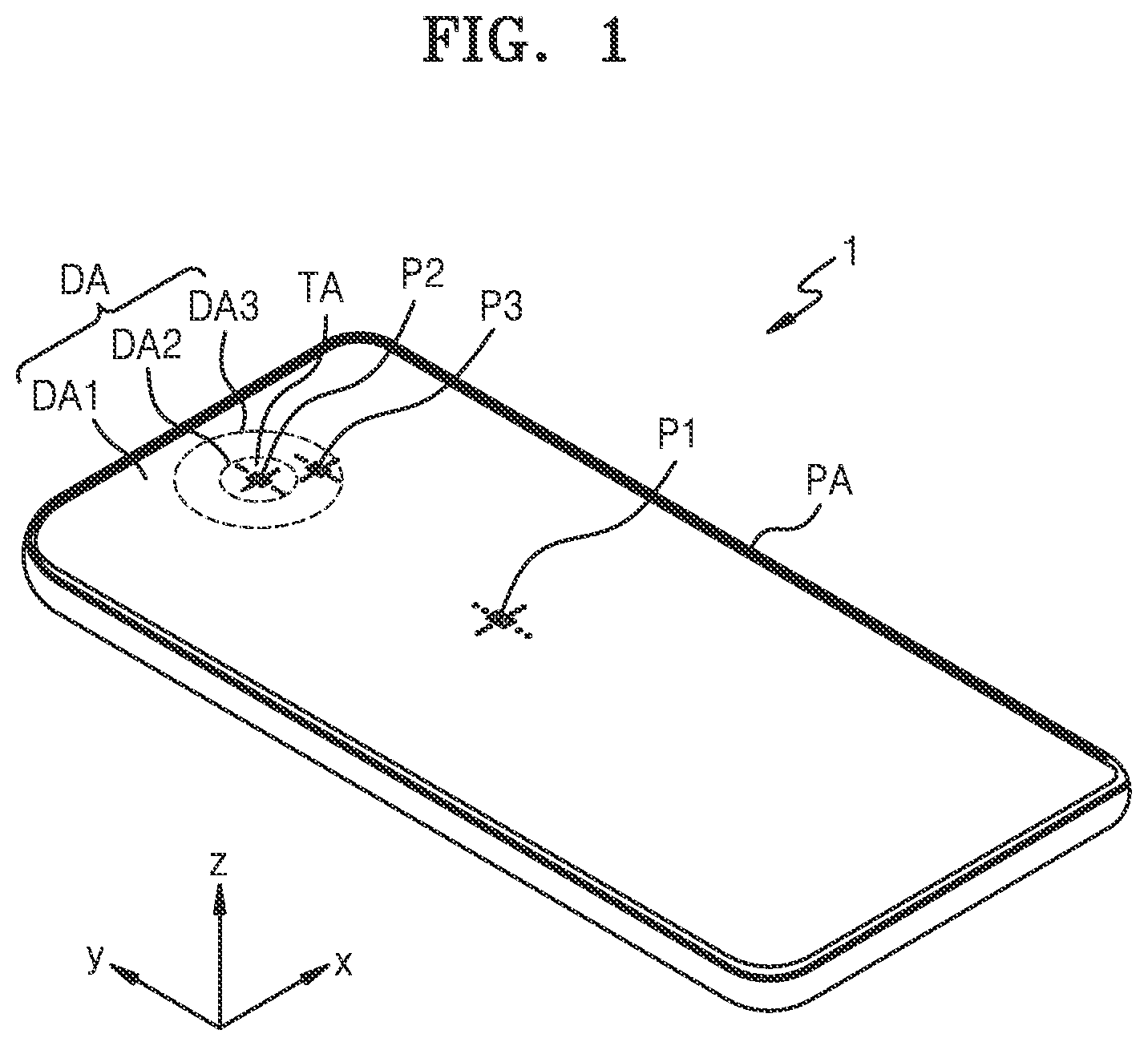
The above and other aspects, features, and characteristics of certain embodiments of the disclosure will be more apparent from the following description taken in conjunction with the accompanying drawings, in which: is a perspective view schematically showing an electronic device according to some embodiments; is a cross-sectional view schematically showing an electronic device according to some embodiments; is a plan view schematically illustrating a display panel according to some embodiments; is an equivalent circuit diagram schematically showing a sub-pixel circuit electrically connected to a light-emitting diode of a display panel, according to some embodiments; is a cross-sectional view showing an electric connection between a first sub-pixel circuit and a first light-emitting diode of a display panel, according to some embodiments; is a cross-sectional view showing an electric connection between a second sub-pixel circuit and a second light-emitting diode of a display panel, according to some embodiments; is a plan view of sub-pixels arranged in a display area of a display panel, according to some embodiments; is a plan view of a portion of a display panel, according to some embodiments; A is a plan view showing a portion VIII of the display panel of , according to some embodiments; B is a plan view showing a portion VIII of the display panel of , according to some embodiments; is a plan view showing second sub-pixel circuits and second light-emitting diodes of a display panel being electrically connected to each other through transparent conductive bus lines, according to some embodiments; A is a cross-sectional view schematically showing a second display area and a third display area of a display panel, according to some embodiments; B is a cross-sectional view schematically showing a second display area and a third display area of a display panel, according to some embodiments; is a plan view showing a second sub-pixel circuit and second light-emitting diodes of a display panel being electrically connected to each other through a transparent conductive bus line and branch conductive bus lines, according to some embodiments; is a cross-sectional view showing a second sub-pixel circuit and second light-emitting diodes of a display panel being electrically connected to each other through a transparent conductive bus line and a branch conductive bus line, according to some embodiments; and is a plan view showing a second sub-pixel circuit and second light-emitting diodes of a display panel being electrically connected to each other through a transparent conductive bus line and branch conductive bus lines, according to some embodiments.
DETAILED DESCRIPTION
The disclosure may have various modifications and various embodiments, and specific embodiments are illustrated in the drawings and are described in detail in the detailed description. Effects and features of embodiments according to the present disclosure and methods of achieving the same will become apparent with reference to embodiments described in detail with reference to the drawings. However, embodiments according to the present disclosure are not limited to the embodiments described below, and may be implemented in various forms. Hereinafter, aspects of some embodiments will be described in more detail with reference to the accompanying drawings, and in the following description with reference to the drawings, like reference numerals refer to like elements and redundant descriptions thereof will be omitted. In the following embodiments, the terms “first” and “second” are not used in a limited sense and are used to distinguish one component from another component. In the following embodiments, an expression used in the singular encompasses the expression of the plural, unless it has a clearly different meaning in the context. In the following embodiments, it will be further understood that the terms “comprise” and/or “comprising” used herein specify the presence of stated features or components, but do not preclude the presence or addition of one or more other features or components. It will be understood that when a layer, region, or element is referred to as being “formed on” another layer, area, or element, it can be directly or indirectly formed on the other layer, region, or element. That is, for example, intervening layers, regions, or elements may be present. In the drawings, for convenience of description, sizes of components may be exaggerated or reduced. In other words, because sizes and thicknesses of components in the drawings are arbitrarily illustrated for convenience of explanation, the disclosure is not necessarily limited thereto. When a certain embodiment may be implemented differently, a specific process order may be performed differently from the described order. For example, two consecutively described processes may be performed substantially at the same time or performed in an order opposite to the described order. In the specification, “A and/or B” denotes only A, only B, or both A and B. Also, “at least one of A and B” or “at least one of A or B” denotes only A, only B, or both A and B. When a layer, region, component, or the like is connected to another layer, region, component, or the like, the layer, the region, the component, or the like may be directly connected thereto and/or may be indirectly connected thereto with an intervening layer, region, component, or the like therebetween. For example, in the specification, when a layer, region, component, or the like is electrically connected to another layer, region, component, or the like, the layer, region, component, or the like may be directly electrically connected thereto and/or may be indirectly electrically connected thereto with an intervening layer, region, component, or the like therebetween. An x-axis, a y-axis, and a z-axis are not limited to three axes on an orthogonal coordinate system, but may be interpreted in a broad sense including the three axes. For example, the x-axis, the y-axis, and the z-axis may be perpendicular to one another, or may represent different directions that are not perpendicular to one another. is a perspective view schematically showing an electronic device 1 according to some embodiments. Referring to , the electronic device 1 may include a display area DA and a peripheral area PA located outside (e.g., in a periphery or outside a footprint of) the display area DA. The display area DA may display images at sub-pixels. The peripheral area PA is a non-display area that is arranged outside the display area DA and does not display images, and may entirely surround the display area DA. A driver or the like for providing an electric signal or power to the display area DA may be arranged in the peripheral area PA. A pad that is a region to which an electronic device or a printed circuit board may be electrically connected may be arranged in the peripheral area PA. Hereinafter, for convenience of description, the electronic device 1 is a smart phone, but the electronic device 1 of embodiments according to the present disclosure is not limited thereto. The electronic device 1 may be applied not only to a portable electronic device, such as a mobile phone, a smart phone, a tablet personal computer (PC), a mobile communication terminal, an electronic notebook, an electronic book, a portable multimedia player (PMP), a navigation device, or an ultra mobile PC (UMPC), but also to any type of product, such as a television, a laptop computer, a monitor, a billboard, or an Internet of things (IoT)-based device. Also, the electronic device 1 according to some embodiments may be applied to a wearable device, such as a smart watch, a watch phone, a glasses-type display, or a head mounted display (HMD). In addition, the electronic device 1 according to some embodiments may be applied to a panel of a vehicle, a center information display (CID) arranged on a center fascia or dashboard of a vehicle, a room mirror display replacing a side mirror of a vehicle, or a display arranged on a rear surface of a front seat, as entertainment for a back seat of a vehicle. The display area DA may include a first display area DA 1 , a second display area DA 2 , and a third display area DA 3 . The display area DA may display images by using sub-pixels arranged 2-dimensionally. The sub-pixels may include first sub-pixels P 1 arranged in the first display area DA 1 , second sub-pixels P 2 arranged in the second display area DA 2 , and third sub-pixels P 3 arranged in the third display area DA 3 . The first display area DA 1 may occupy the most area of the display area DA. Occupying the most area may indicate that the area of the first display area DA 1 is equal to or greater than about 50% of the area of the display area DA. The second display area DA 2 may be arranged inside the display area DA. For example, the second display area DA 2 may be entirely surrounded by the first display area DA 1 . The third display area DA 3 may be arranged between the first display area DA 1 and the second display area DA 2 . The third display area DA 3 may entirely surround the second display area DA 2 , and may be entirely surrounded by the first display area DA 1 . Each of the second display area DA 2 and the third display area DA 3 may have an area smaller than the first display area DA 1 . According to some embodiments, illustrates that the second display area DA 2 and the third display area DA 3 each have a circular shape. According to some embodiments, the second display area DA 2 and the third display area DA 3 may each have an approximately rectangular shape. In , the second display area DA 2 and the third display area DA 3 are arranged at an upper center (in a +y direction) of the display area DA having an approximately rectangular shape, when viewed in a direction approximately perpendicular or normal (e.g., when viewed in a plan view) to a top surface of the electronic device 1 , but embodiments according to the present disclosure are not limited thereto. The second display area DA 2 and the third display area DA 3 may be arranged, for example, at an upper right or upper left side of the display area DA. The second display area DA 2 may display images through the second sub-pixels P 2 , and transmit light or sound through a region between the second sub-pixels P 2 . Hereinafter, a region at which light or sound may penetrate is referred to as a transmission area TA. In other words, the second display area DA 2 may include the transmission area TA between the second sub-pixels P 2 . is a cross-sectional view schematically showing the electronic device 1 according to some embodiments. Referring to , the electronic device 1 may include a display panel 10 and a component 20 overlapping the display panel 10 . The component 20 may be arranged in the second display area DA 2 . The component 20 may be an electronic element using light or sound. For example, the electronic element may be a sensor measuring a distance, such as a proximity sensor, a sensor recognizing a part (for example, a fingerprint, an iris, or a face) of a body of a user, a small lamp outputting light, or an image sensor (for example, a camera) capturing an image. The electronic element using light may use light of various wavelength bands, such as visible light, infrared light, or ultraviolet light. The electronic element using sound may use ultrasonic waves or sound in another frequency band. The second display area DA 2 may include the transmission area TA through which light and/or sound output to the outside from the component 20 or proceeding from the outside towards the component 20 may penetrate. According to some embodiments, the transmission area TA is a region where light may penetrate, and may correspond to a region between the second sub-pixels P 2 . In the electronic device 1 according to some embodiments, when light is transmitted through the second display area DA 2 including the transmission area TA, light transmittance may be equal to or greater than about 10%, equal to or greater than 25%, equal to or greater than 40%, equal to or greater than 50%, equal to or greater than 85%, or equal to or greater than 90%. Each of the first sub-pixel P 1 , the second sub-pixel P 2 , and the third sub-pixel P 3 , which are described above with reference to , may emit light by using a light-emitting diode, and each light-emitting diode may be arranged in the display area DA of the display panel 10 . In this regard, a light-emitting diode corresponding to the first sub-pixel P 1 of the first display area DA 1 may be referred to as a first light-emitting diode ED 1 , a light-emitting diode corresponding to the second sub-pixel P 2 of the second display area DA 2 may be referred to as a second light-emitting diode ED 2 , and a light-emitting diode corresponding to the third sub-pixel P 3 of the third display area DA 3 may be referred to as a third light-emitting diode ED 3 . The first through third light-emitting diodes ED 1 through ED 3 may be located on a substrate 100 . The substrate 100 may include an insulating material, such as a glass material or polymer resin, and a protection film PB may be located on a rear surface of the substrate 100 . The substrate 100 may be a rigid substrate or a flexible substrate capable of being bent, folded, or rolled. The protection film PB may include an opening PB-OP located in the second display area DA 2 to enhance transmittance of the transmission area TA. A sub-pixel circuit layer 200 including a first sub-pixel circuit PC 1 , a second sub-pixel circuit PC 2 and a third sub-pixel circuit PC 1 may be located on a front surface of the substrate 100 . The first light-emitting diode ED 1 is arranged in the first display area DA 1 and is electrically connected to a first sub-pixel circuit PC 1 arranged in the first display area DA 1 . The first sub-pixel circuit PC 1 may include transistors and a storage capacitor electrically connected to the transistors. The second light-emitting diode ED 2 is arranged in the second display area DA 2 . The second light-emitting diode ED 2 is electrically connected to a second sub-pixel circuit PC 2 , and the second sub-pixel circuit PC 2 is not arranged in the second display area DA 2 so as to enhance the transmittance and transmissive surface area of the transmission area TA provided in the second display area DA 2 . The second sub-pixel circuit PC 2 is arranged in the third display area DA 3 , and the second light-emitting diode ED 2 may be electrically connected to the second sub-pixel circuit PC 2 through a transparent conductive bus line CBL. The transparent conductive bus line CBL may electrically connect the second sub-pixel circuit PC 2 of the third display area DA 3 and the second light-emitting diode ED 2 of the second display area DA 2 to each other. The transparent conductive bus line CBL may include a light-transmitting material, for example, a transparent conductive oxide (TCO). The TCO may include indium tin oxide (ITO), indium zinc oxide (IZO), zinc oxide (ZnO), indium oxide (In 2 O 3 ), indium gallium oxide (IGO), and/or aluminum zinc oxide (AZO). The third light-emitting diode ED 3 is arranged in the third display area DA 3 and is electrically connected to a third sub-pixel circuit PC 3 arranged in the third display area DA 3 . The third sub-pixel circuit PC 3 may include transistors and a storage capacitor electrically connected to the transistors. The first through third light-emitting diodes ED 1 through ED 3 are light-emitting elements that emit light of a certain color, and may include organic light-emitting diodes. According to some embodiments, the first through third light-emitting diodes ED 1 through ED 3 may include inorganic light-emitting diodes or may be light-emitting diodes including quantum dots. The first through third light-emitting diodes ED 1 through ED 3 may be covered by an encapsulation layer 300 . The encapsulation layer 300 may be a thin-film encapsulation layer including an inorganic encapsulation layer including an inorganic insulating material, and an organic encapsulation layer including an organic insulating material. According to some embodiments, the encapsulation layer 300 may include first and second inorganic encapsulation layers and an organic encapsulation layer therebetween. According to some embodiments, the encapsulation layer 300 may be an encapsulation substrate of a glass material. A sealant including frit or the like may be arranged between the substrate 100 and the encapsulation substrate. The sealant may be located in the peripheral area PA (refer to ) while extending to surround an outer edge of the display area DA, thereby preventing or reducing instances of contaminants or moisture penetrating into the first through third light-emitting diodes ED 1 through ED 3 through a side surface. An input detection layer 400 may be located on the encapsulation layer 300 . The input detection layer 400 may obtain coordinate information according to an external input, for example, a touch event of an object, such as a finger or a stylus pen. The input detection layer 400 may include a touch electrode and trace wires connected to the touch electrode. The input detection layer 400 may detect an external input via a mutual cap method or a self-cap method. An optical functional layer 500 may include an antireflection layer. The antireflection layer may reduce reflectance of light (external light) incident from the outside towards the display panel 10 through a cover window 600 . The antireflection layer may include a retarder and a polarizer. When the optical functional layer 500 includes the polarizer, the optical functional layer 500 may include an opening 510 located in the second display area DA 2 , thereby enhancing transmittance of the transmission area TA. According to some embodiments, the antireflection layer may include a black matrix and color filters. The color filters may be arranged considering a color of light emitted from each of the first through third light-emitting diodes ED 1 through ED 3 . When the optical functional layer 500 includes the black matrix and the color filters, a light-transmitting material may be arranged at a location corresponding to the transmission area TA. According to some embodiments, the antireflection layer may include a destructive interference structure. The destructive interference structure may include a first reflective layer and a second reflective layer arranged on different layers. A first reflective light and a second reflective light reflected respectively from the first reflective layer and the second reflective layer may destructively interfere with each other, and accordingly, reflectance of an external light may be reduced. The cover window 600 may be located on the optical functional layer 500 . The cover window 600 may be combined with the optical functional layer 500 through an adhesive layer, such as an optically clear adhesive, arranged between the cover window 600 and the optical functional layer 500 . The cover window 600 may include a glass material or a plastic material. The plastic material may include polyether sulfone, polyacrylate, polyether imide, polyethylene naphthalate, polyethylene terephthalate, polyphenylene sulfide, polyarylate, polyimide, polycarbonate, or cellulose acetate propionate. The cover window 600 may include a flexible cover window. For example, the cover window 600 may include polyimide and/or ultra-thin glass. is a plan view schematically illustrating the display panel 10 according to some embodiments. Referring to , the display panel 10 may include the display area DA and the peripheral area PA. The display area DA may include the first display area DA 1 , the second display area DA 2 , and the third display area DA 3 . The display area DA, for example, the first display area DA 1 , second display area DA 2 , and third display area DA 3 , may correspond to an image surface of the display panel 10 . The second and third display areas DA 2 and DA 3 may be spaced apart from a virtual line IML passing through a center of the display area DA and/or a center of the image surface. For example, a center of the second display area DA 2 and a center of the third display area DA 3 may be arranged on the virtual line IML passing through the center of the display area DA and/or the center of the image surface as shown in , but according to some embodiments, the centers of the second and third display areas DA 2 and DA 3 may be spaced apart from the virtual line IML in a left or right direction. Light-emitting diodes are arranged in the first through third display areas DA 1 through DA 3 , and sub-pixel circuits electrically connected to the light-emitting diodes respectively are arranged in the first display area DA 1 and the third display area DA 3 , but are not arranged in the second display area DA 2 . For example, the first sub-pixel circuits PC 1 electrically connected to the first light-emitting diodes ED 1 arranged in the first display area DA 1 are arranged in the first display area DA 1 , and the second and third sub-pixel circuits PC 2 and PC 3 electrically connected to the second and third light-emitting diodes ED 2 and ED 3 arranged in the second and third display areas DA 2 and DA 3 may be arranged in the third display area DA 3 . In other words, a portion (for example, the second sub-pixel circuits PC 2 ) of sub-pixel circuits arranged in the third display area DA 3 may be electrically connected to the second light-emitting diodes ED 2 arranged in the second display area DA 2 , and another portion (for example, the third sub-pixel circuits PC 3 ) of the sub-pixel circuits arranged in the third display area DA 3 may be electrically connected to the third light-emitting diodes ED 3 arranged in the third display area DA 3 . Hereinafter, for convenience of descriptions, sub-pixel circuits electrically connected to the second light-emitting diodes ED 2 from among the sub-pixel circuits arranged in the third display area DA 3 are referred to as the second sub-pixel circuits PC 2 , and sub-pixel circuits electrically connected to the third light-emitting diodes ED 3 from among the sub-pixel circuits arranged in the third display area DA 3 are referred to as the third sub-pixel circuits PC 3 . The first light-emitting diode ED 1 is arranged in the first display area DA 1 . Light emitted from the first light-emitting diode ED 1 corresponds to light of the first sub-pixel P 1 of described with reference to , and a location of the first light-emitting diode ED 1 may be a location of the first sub-pixel P 1 of . The first light-emitting diode ED 1 may emit, for example, red, green, or blue light. The first sub-pixel circuit PC 1 driving the first light-emitting diode ED 1 may be arranged in the first display area DA 1 and electrically connected to the first light-emitting diode ED 1 . The first sub-pixel circuit PC 1 is electrically connected to a scan line SL extending in a first direction (for example, an x direction), and a data line DL extending in a second direction (for example, a y direction). A first driving circuit SDRV 1 and a second driving circuit SDRV 2 for providing a signal to each first sub-pixel circuit PC 1 may be arranged in the peripheral area PA. The first driving circuit SDRV 1 may apply a scan signal to each of the first sub-pixel circuits PC 1 through the scan line SL. The second driving circuit SDRV 2 may be located opposite to the first driving circuit SDRV 1 based on the first display area DA 1 therebetween. Some of the first sub-pixel circuits PC 1 of the first display area DA 1 may be electrically connected to the first driving circuit SDRV 1 and the remaining ones may be electrically connected to the second driving circuit SDRV 2 . A pad PAD may be arranged at one side of the substrate 100 . The pad PAD may not be covered by an insulating layer, but may be exposed and connected to a circuit board 30 . A control driving unit 32 may be arranged in the circuit board 30 . The control driving unit 32 may be configured to generate a control signal transmitted to the first driving circuit SDRV 1 and the second driving circuit SDRV 2 . The control driving unit 32 may include a data driving circuit and the data driving circuit may be configured to generate a data signal. The generated data signal may be transmitted to the first sub-pixel circuits PC 1 through a fanout wire FW arranged in the peripheral area PA of the display panel 10 , and the data line DL connected to the fanout wire FW. According to some embodiments, the data driving circuit may be arranged in the peripheral area PA of the substrate 100 . The second light-emitting diode ED 2 is arranged in the second display area DA 2 . Light emitted from the second light-emitting diode ED 2 corresponds to light of the second sub-pixel P 2 of described with reference to , and a location of the second light-emitting diode ED 2 may be a location of the second sub-pixel P 2 of . The second light-emitting diode ED 2 may emit, for example, red, green, or blue light. The transmission area TA may be arranged between the second light-emitting diodes ED 2 . According to some embodiments, a region of the second display area DA 2 , where the second light-emitting diodes ED 2 are not arranged, may correspond to the transmission area TA. To increase the area and enhance the transmittance of the transmission area TA, the second sub-pixel circuit PC 2 for driving the second light-emitting diode ED 2 may be arranged in the third display area DA 3 outside the second display area DA 2 . A portion of the second sub-pixel circuits PC 2 may be arranged in a partial region of the third display area DA 3 adjacent to the top of the second display area DA 2 , and another portion of the second sub-pixel circuits PC 2 may be arranged in a partial region of the third display area DA 3 adjacent to the bottom of the second display area DA 2 . The second sub-pixel circuit PC 2 in the third display area DA 3 may be electrically connected to the second light-emitting diode ED 2 in the second display area DA 2 , through the transparent conductive bus line CBL. The second light-emitting diode ED 2 may be electrically connected to the second sub-pixel circuit PC 2 through the transparent conductive bus line CBL extending in the second direction (for example, the y direction). The third light-emitting diode ED 3 may be arranged in the third display area DA 3 . Light emitted from the third light-emitting diode ED 3 corresponds to light of the third sub-pixel P 3 of described with reference to , and a location of the third light-emitting diode ED 3 may be a location of the third sub-pixel P 3 of . The third light-emitting diode ED 3 may emit, for example, red, green, or blue light. The third sub-pixel circuit PC 3 for driving the third light-emitting diode ED 3 is arranged in the third display area DA 3 . The third sub-pixel circuit PC 3 is electrically connected to the third light-emitting diode ED 3 and may operate the third light-emitting diode ED 3 . The second sub-pixel circuit PC 2 and the third sub-pixel circuit PC 3 may be electrically connected to the first driving circuit SDRV 1 and/or the second driving circuit SDRV 2 . At least one second sub-pixel circuit PC 2 and/or at least one third sub-pixel circuit PC 3 may share a scan line with at least one first sub-pixel circuit PC 1 . At least one second sub-pixel circuit PC 2 and/or at least one third sub-pixel circuit PC 3 may share a data line with at least one first sub-pixel circuit PC 1 . A driving voltage supply line 11 and a common voltage supply line 13 may be arranged in the peripheral area PA. The driving voltage supply line 11 may apply a driving voltage to each sub-pixel circuit, for example, each of the first through third sub-pixel circuits PC 1 through PC 3 , and the common voltage supply line 13 may apply a common voltage to a second electrode (cathode) of each light-emitting diode, for example, each of the first through third light-emitting diodes ED 1 through ED 3 . The driving voltage supply line 11 may be arranged between the pad PAD and one side of the display area DA. The common voltage supply line 13 may have a loop shape with one opened side, and partially surround the display area DA in a plan view. The driving voltage supply line 11 may be electrically connected to a driving voltage line PL passing through the display area DA. The first through third light-emitting diodes ED 1 through ED 3 , the first through third sub-pixel circuits PC 1 through PC 3 , the pad PAD, the first and second driving circuits SDRV 1 and SDRV 2 , the driving voltage supply line 11 , and the common voltage supply line 13 are located on the substrate 100 . A shape of the display panel shown in may be substantially the same as a shape of the substrate 100 . Accordingly, the display panel 10 including the display area DA and the peripheral area PA may indicate that the substrate 100 includes the display area DA and the peripheral area PA. is an equivalent circuit diagram schematically showing a sub-pixel circuit PC electrically connected to a light-emitting diode ED of a display panel, according to some embodiments. The light-emitting diode ED of may correspond to the first through third light-emitting diodes ED 1 through ED 3 described above with reference to , and the sub-pixel circuit PC of may correspond to the first through third sub-pixel circuits PC 1 through PC 3 described above with reference to . In other words, an equivalent circuit diagram of the first light-emitting diode ED 1 of and the first sub-pixel circuit PC 1 , an equivalent circuit diagram of the second light-emitting diode ED 2 of and the second sub-pixel circuit PC 2 , and an equivalent circuit diagram of the third light-emitting diode ED 3 of and the third sub-pixel circuit PC 3 may be the same. As described above, the light-emitting diode ED may include an organic light-emitting diode, an inorganic light-emitting diode, or a quantum dot light-emitting diode. The light-emitting diode ED may be electrically connected to the sub-pixel circuit PC. Referring to , the sub-pixel circuit PC may include first through seventh transistors T 1 through T 7 , a storage capacitor Cst, and a boost capacitor Cbt. According to some embodiments, the sub-pixel circuit PC may not include the boost capacitor Cbt, and hereinafter, for convenience of descriptions, the sub-pixel circuit PC includes the boost capacitor Cbt. Additionally, in some embodiments according to the present disclosure, the sub-pixel circuit PC may include additional components or fewer components without departing from the spirit and scope of embodiments according to the present disclosure. Some of the first through seventh transistors T 1 through T 7 may be n-channel MOSFETs (NMOSs) and the remaining ones may be p-channel MOSFETs (PMOSs). For example, as shown in , the third and fourth transistors T 3 and T 4 may be NMOSs and the remaining ones may be PMOSs. According to some embodiments, the third, fourth, and seventh transistors T 3 , T 4 , and T 7 may be NMOSs and the remaining ones may be PMOSs. Alternatively, only one of the first through seventh transistors T 1 through T 7 may be an NMOS and the remaining ones may be PMOSs. The first through seventh transistors T 1 through T 7 , the storage capacitor Cst, and the boost capacitor Cbt may be connected to a signal line. The signal line may include the scan line SL, an emission control line EL, and the data line DL. The scan line SL may include a first scan line SL 1 configured to transmit a first scan signal Sn, a second scan line SL 2 configured to transmit a second scan signal Sn′, a previous scan line SLp configured to transmit a previous scan signal Sn−1, and a next scan line SLn configured to transmit a next scan signal Sn+1. The driving voltage line PL is configured to transmit a driving voltage ELVDD to the first transistor T 1 , and first and second initialization voltage lines 145 and 165 may be configured to transmit first and second initialization voltages Vint 1 and Vint 2 , respectively. The first transistor T 1 may be a driving transistor. A first gate electrode of the first transistor T 1 may be connected to the storage capacitor Cst, a first electrode of the first transistor T 1 may be electrically connected to the driving voltage line PL through the fifth transistor T 5 , and a second electrode of the first transistor T 1 may be electrically connected to a first electrode (for example, an anode) of the light-emitting diode ED through the sixth transistor T 6 . One of the first electrode and second electrode of the first transistor T 1 may be a source electrode and the other one may be a drain electrode. The first transistor T 1 may supply a driving current Id to the light-emitting diode ED according to a switching operation of the second transistor T 2 . The second transistor T 2 may be a switching transistor. A second gate electrode of the second transistor T 2 may be connected to the first scan line SL 1 , a first electrode of the second transistor T 2 may be connected to the data line DL, and a second electrode of the second transistor T 2 may be connected to the first electrode of the first transistor T 1 while being electrically connected to the driving voltage line PL through the fifth transistor T 5 . One of the first electrode and second electrode of the second transistor T 2 may be a source electrode and the other one may be a drain electrode. The second transistor T 2 may be turned on according to the first scan signal Sn received through the first scan line SL 1 to perform the switching operation of transmitting a data signal Dm transmitted to the data line DL, to the first electrode of the first transistor T 1 . The third transistor T 3 may be a compensation transistor configured to compensate for a threshold voltage of the first transistor T 1 . A third gate electrode of the third transistor T 3 is connected to the second scan line SL 2 . A first electrode of the third transistor T 3 is connected to the first gate electrode of the first transistor T 1 and a lower electrode CE 1 of the storage capacitor Cst, through a node connection line 166 . The first electrode of the third transistor T 3 may be connected to the fourth transistor T 4 . A second electrode of the third transistor T 3 may be connected to the second electrode of the first transistor T 1 while being electrically connected to the first electrode (for example, an anode) of the light-emitting diode ED through the sixth transistor T 6 . One of the first electrode and second electrode of the third transistor T 3 may be a source electrode and the other one may be a drain electrode. The third transistor T 3 may be turned on according to the second scan signal Sn′ (for example, a compensation control signal) received through the second scan line SL 2 to electrically connect the second electrode to the first gate electrode of the first transistor T 1 , thereby diode-connecting the first transistor T 1 . The fourth transistor T 4 may be a first initialization transistor configured to initialize the first gate electrode of the first transistor T 1 . A fourth gate electrode of the fourth transistor T 4 is connected to the previous scan line SLp. The first electrode of the fourth transistor T 4 is connected to the first initialization voltage line 145 . A second electrode of the fourth transistor T 4 may be connected to the lower electrode CE 1 of the storage capacitor Cst, the first electrode of the third transistor T 3 , and the first gate electrode of the first transistor T 1 . One of the first electrode and second electrode of the fourth transistor T 4 may be a source electrode and the other one may be a drain electrode. The fourth transistor T 4 may be turned on according to the previous scan signal Sn−1 received through the previous scan line SLp, and perform an initialization operation of initializing a voltage of the first gate electrode of the first transistor T 1 by transmitting the first initialization voltage Vint 1 to the first gate electrode of the first transistor T 1 . The fifth transistor T 5 may be an operation control transistor. A fifth gate electrode of the fifth transistor T 5 may be connected to the emission control line EL, a first electrode of the fifth transistor T 5 may be connected to the driving voltage line PL, and a second electrode of the fifth transistor T 5 may be connected to the first electrode of the first transistor T 1 and the second electrode of the second transistor T 2 . One of the first electrode and second electrode of the fifth transistor T 5 may be a source electrode and the other one may be a drain electrode. The sixth transistor T 6 may be an emission control transistor. A sixth gate electrode of the sixth transistor T 6 may be connected to the emission control line EL, a first electrode of the sixth transistor T 6 may be connected to the second electrode of the first transistor T 1 and the second electrode of the third transistor T 3 , and a second electrode of the sixth transistor T 6 may be electrically connected to a second electrode of the seventh transistor T 7 and the first electrode (for example, an anode) of the light-emitting diode ED. One of the first electrode and second electrode of the sixth transistor T 6 may be a source electrode and the other one may be a drain electrode. The fifth transistor T 5 and the sixth transistor T 6 may be simultaneously turned on according to an emission control signal En received through the emission control line EL to transmit the driving voltage ELVDD to the light-emitting diode ED such that the driving current Id flows in the light-emitting diode ED. The seventh transistor T 7 may be a second initialization transistor configured to initialize the first electrode (for example, an anode) of the light-emitting diode ED. A seventh gate electrode of the seventh transistor T 7 is connected to the next scan line SLn. A first electrode of the seventh transistor T 7 is connected to the second initialization voltage line 165 . The second electrode of the seventh transistor T 7 is connected to the second electrode of the sixth transistor T 6 and the first electrode (for example, an anode) of the light-emitting diode ED. The seventh transistor T 7 may be turned on according to the next scan signal Sn+1 received through the next scan line SLn to transmit the second initialization voltage Vint 2 to the first electrode (for example, an anode) of the light-emitting diode ED so as to initialize the first electrode of the light-emitting diode ED. In , the seventh transistor T 7 is connected to the next scan line SLn, but the seventh transistor T 7 may be connected to the previous scan line SLp. The storage capacitor Cst may include the lower electrode CE 1 and an upper electrode CE 2 . The lower electrode CE 1 of the storage capacitor Cst is connected to the first gate electrode of the first transistor T 1 , and the upper electrode CE 2 of the storage capacitor Cst is connected to the driving voltage line PL. The storage capacitor Cst may store charges corresponding to a difference between a voltage of the first gate electrode of the first transistor T 1 and the driving voltage ELVDD. The boost capacitor Cbt includes a third electrode CE 3 and a fourth electrode CE 4 . The third electrode CE 3 may be connected to the first scan line SL 1 and the second gate electrode of the second transistor T 2 , and the fourth electrode CE 4 may be connected to the node connection line 166 and the first electrode of the third transistor T 3 . When the first scan signal Sn supplied to the first scan line SL 1 is turned off (e.g., an off level), the boost capacitor Cbt may raise a voltage of a first node N 1 , and when the voltage of the first node N 1 is raised, black gradation may be clearly represented. The first node N 1 may be a region where the first gate electrode of the first transistor T 1 , the first electrode of the third transistor T 3 , the second electrode of the fourth transistor T 4 , and the fourth electrode CE 4 of the boost capacitor Cbt are connected to each other. According to some embodiments, in , the third and fourth transistors T 3 and T 4 are NMOSs, and the first, second, fifth, sixth, and seventh transistors T 1 , T 2 , T 5 , T 6 , and T 7 are PMOSs. The first transistor T 1 that directly affects brightness of the display device includes a semiconductor layer including polycrystalline silicon having high reliability so that the display device having high resolution is realized. In , the third and fourth transistors T 3 and T 4 are NMOSs, but according to some embodiments, the first through seventh transistors T 1 through T 7 may be PMOSs. In this case, the second and third transistors T 2 and T 3 may be electrically connected to a same scan line. According to some embodiments, the fourth and seventh transistors T 4 and T 7 may also be electrically connected to a same scan line. According to some embodiments, the fourth and seventh transistors T 4 and T 7 may be electrically connected to a same initialization voltage line. is a cross-sectional view showing an electric connection between the first sub-pixel circuit PC 1 and the first light-emitting diode ED 1 of the display panel 10 , according to some embodiments. Referring to , the first sub-pixel circuit PC 1 located on the substrate 100 , and the first light-emitting diode ED 1 on the first sub-pixel circuit PC 1 may be located in the first display area DA 1 of the display panel 10 . As described above with reference to , the substrate 100 may include a glass material or polymer resin. A buffer layer 201 may be located on the substrate 100 . The buffer layer 201 may prevent or reduce instances of contaminants or impurities penetrating into a semiconductor layer of a transistor. The buffer layer 201 may include an inorganic insulating material, such as silicon nitride, silicon oxynitride, or silicon oxide, and may be a single layer or multilayer including the above inorganic insulating material. The first sub-pixel circuit PC 1 may be arranged on the buffer layer 201 . As described above with reference to , the first sub-pixel circuit PC 1 may include a plurality of thin-film transistors and a storage capacitor. In this regard, illustrates the first transistor T 1 , the third transistor T 3 , the sixth transistor T 6 , and the storage capacitor Cst. The first transistor T 1 may include a first semiconductor layer A 1 on the buffer layer 201 , and a first gate electrode GE 1 overlapping a channel region C 1 of the first semiconductor layer A 1 . The first semiconductor layer A 1 may include a silicon-based semiconductor material, for example, polysilicon. The first semiconductor layer A 1 may include the channel region C 1 , and a first region B 1 and a second region D 1 , which are arranged on both sides of the channel region C 1 . The first region B 1 and the second region D 1 are regions including higher concentration of impurities than the channel region C 1 , and one of the first region B 1 and the second region D 1 may correspond to a source region and the other one may correspond to a drain region. The sixth transistor T 6 may include a sixth semiconductor layer A 6 on the buffer layer 201 , and a sixth gate electrode GE 6 overlapping a channel region C 6 of the sixth semiconductor layer A 6 . The sixth semiconductor layer A 6 may include a silicon-based semiconductor material, for example, polysilicon. The sixth semiconductor layer A 6 may include the channel region C 6 , and a first region B 6 and a second region D 6 , which are arranged on both sides of the channel region C 6 . The first region B 6 and the second region D 6 are regions including higher concentration of impurities than the channel region C 6 , and one of the first region B 6 and the second region D 6 may correspond to a source region and the other one may correspond to a drain region. The first gate electrode GE 1 and the sixth gate electrode GE 6 may include a conductive material including molybdenum (Mo), aluminum (Al), copper (Cu), or titanium (Ti), and may be formed in a single layer or multilayer structure including the conductive material. A first gate insulating layer 203 for electric insulation between the first semiconductor layer A 1 and the sixth semiconductor layer A 6 may be located below the first gate electrode GE 1 and the sixth gate electrode GE 6 . The first gate insulating layer 203 may include an inorganic insulating material, such as silicon nitride, silicon oxynitride, or silicon oxide, and may be a single layer or multilayer including the above inorganic insulating material. The storage capacitor Cst may include the lower electrode CE 1 and the upper electrode CE 2 that overlap each other. According to some embodiments, the lower electrode CE 1 of the storage capacitor Cst may include the first gate electrode GE 1 . In other words, the first gate electrode GE 1 may include the lower electrode CE 1 of the storage capacitor Cst. For example, the first gate electrode GE 1 may be integrated with the lower electrode CE 1 of the storage capacitor Cst. A first interlayer insulating layer 205 may be arranged between the lower electrode CE 1 and upper electrode CE 2 of the storage capacitor Cst. The first interlayer insulating layer 205 may include an inorganic insulating material, such as silicon oxide, silicon nitride, or silicon oxynitride, and may include a single layer or multilayer structure including the above inorganic insulating material. The upper electrode CE 2 of the storage capacitor Cst may include a low-resistance conductive material such as molybdenum (Mo), aluminum (Al), copper (Cu), and/or titanium (Ti), and may include a single layer or multilayer structure including such a material. A second interlayer insulating layer 207 may be located on the storage capacitor Cst. The second interlayer insulating layer 207 may include an inorganic insulating material, such as silicon oxide, silicon nitride, or silicon oxynitride, and may include a single layer or multilayer structure including the above inorganic insulating material. A third semiconductor layer A 3 of the third transistor T 3 may be located on the second interlayer insulating layer 207 . The third semiconductor layer A 3 may include an oxide semiconductor. For example, the third semiconductor layer A 3 may include, a zinc (Zn) oxide-based material, such as a Zn oxide, an In—Zn oxide, or a Ga—In—Zn oxide. According to some embodiments, the third semiconductor layer A 3 may include an In—Ga—Zn—O (IGZO), In—Sn—Zn—O (ITZO), or an In—Ga—Sn—Zn—O (IGTZO) semiconductor, wherein a metal, such as indium (In), gallium (Ga), or tin (Sn) is contained in ZnO. The third semiconductor layer A 3 may include a channel region C 3 , and a first region B 3 and a second region D 3 , which are arranged on both sides of the channel region C 3 . One of the first region B 3 and the second region D 3 may correspond to a source region, and the other one may correspond to a drain region. The third transistor T 3 may include a third gate electrode GE 3 overlapping the channel region C 3 of the third semiconductor layer A 3 . The third gate electrode GE 3 may include a double gate structure including a lower gate electrode G 3 A located below the third semiconductor layer A 3 and an upper gate electrode G 3 B arranged on (e.g., above) the channel region C 3 . The lower gate electrode G 3 A may be arranged on a same layer (for example, the first interlayer insulating layer 205 ) as the upper electrode CE 2 of the storage capacitor Cst. The lower gate electrode G 3 A may include a same material as the upper electrode CE 2 of the storage capacitor Cst. The upper gate electrode G 3 B may be arranged on the third semiconductor layer A 3 with a second gate insulating layer 209 therebetween. The second gate insulating layer 209 may include an inorganic insulating material, such as silicon oxide, silicon nitride, or silicon oxynitride, and may include a single layer or multilayer structure including the above inorganic insulating material. A third interlayer insulating layer 210 may be located on the upper gate electrode G 3 B. The third interlayer insulating layer 210 may include an inorganic insulating material such as silicon oxynitride, and may include a single layer or multilayer structure including the above inorganic insulating material. In , the upper electrode CE 2 of the storage capacitor Cst is arranged on a same layer as the lower gate electrode G 3 A of the third gate electrode GE 3 , but the disclosure is not limited thereto. According to some embodiments, the upper electrode CE 2 of the storage capacitor Cst may be arranged on a same layer as the third semiconductor layer A 3 , and include a same material as the first region B 3 and second region D 3 of the third semiconductor layer A 3 . The first transistor T 1 and the third transistor T 3 may be electrically connected to each other through a node connection line 166 . The node connection line 166 may be located on the third interlayer insulating layer 210 . One side of the node connection line 166 may be connected to the first gate electrode GE 1 of the first transistor T 1 , and the other side of the node connection line 166 may be connected to the first region B 3 of the third semiconductor layer A 3 of the third transistor T 3 . The node connection line 166 may include Al, Cu, and/or Ti, and include a single layer or multilayer including the above material. For example, the node connection line 166 may have a 3-layer structure of a titanium layer/aluminum layer/titanium layer. A first organic insulating layer 211 may be located on the node connection line 166 . The first organic insulating layer 211 may include an organic insulating material. The organic insulating material may include acryl, benzo cyclobutene (BCB), polyimide, or hexamethyldisiloxane (HMDSO). The data line DL and driving voltage line PL may be located on the first organic insulating layer 211 . The data line DL and driving voltage line PL may include Al, Cu, and/or Ti, and include a single layer or multilayer including the above material. For example, the data line DL and driving voltage line PL may have a three-layer structure of titanium layer/aluminum layer/titanium layer. In , the data line DL and driving voltage line PL are arranged on a same layer (for example, the first organic insulating layer 211 ), but according to some embodiments, the data line DL and driving voltage line PL may be arranged on different layers. A second organic insulating layer 212 , a third organic insulating layer 213 , and a fourth organic insulating layer 214 may be located on the first organic insulating layer 211 . The second organic insulating layer 212 , third organic insulating layer 213 , and fourth organic insulating layer 214 may each include an organic insulating material such as acryl, BCB, polyimide, or HMDSO. A first electrode 221 of the first light-emitting diode ED 1 may be located on the fourth organic insulating layer 214 . The first electrode 221 may be electrically connected to the sixth transistor T 6 through a first contact metal CM 1 , a second contact metal CM 2 , a third contact metal CM 3 , and a fourth contact metal CM 4 . The first contact metal CM 1 may be formed on a same layer as the node connection line 166 and include a same material as the node connection line 166 . The second contact metal CM 2 may be formed on a same layer as the data line DL and/or the driving voltage line PL, and include a same material as the data line DL and/or the driving voltage line PL. The third contact metal CM 3 and fourth contact metal CM 4 may include a conductive material, for example, a metal (for example, a non-transmissive metal) or a light-transmissive conductive material. The first electrode 221 may include a reflective layer including silver (Ag), magnesium (Mg), aluminum (Al), platinum (Pt), palladium (Pd), gold (Au), nickel (Ni), neodymium (Nd), iridium (Ir), chromium (Cr), or a compound thereof. According to some embodiments, the first electrode 221 may further include a conductive oxide layer on and/or below the reflective layer. The conductive oxide layer may include indium tin oxide (ITO), indium zinc oxide (IZO), zinc oxide (ZnO), indium oxide (In 2 O 3 ), indium gallium oxide (IGO), and/or aluminum zinc oxide (AZO). According to some embodiments, the first electrode 221 may include a plurality of sub-layers. For example, the first electrode 221 may include a first sub-layer 221 a , a second sub-layer 221 b , and a third sub-layer 221 c . The first sub-layer 221 a , the second sub-layer 221 b , and the third sub-layer 221 c may respectively be an ITO layer, an Ag layer, and an ITO layer. A bank layer 215 may be located on the first electrode 221 . The bank layer 215 includes an opening overlapping the first electrode 221 and may cover an edge of the first electrode 221 . The bank layer 215 may include an organic insulating material, such as polyimide. A spacer 217 may be formed on the bank layer 215 . The spacer 217 may be formed together with the bank layer 215 during a same process or formed individually from the bank layer 215 through a separate process. According to some embodiments, the spacer 217 may include an organic insulating material, such as polyimide. According to some embodiments, the bank layer 215 may include an organic insulating material including a light-shielding dye, and the spacer 217 may include an organic insulating material such as polyimide. An intermediate layer 222 includes an emission layer 222 b . The intermediate layer 222 may include a first functional layer 222 a located below the emission layer 222 b and/or a second functional layer 222 c located on the emission layer 222 b . The emission layer 222 b may include a high-molecular weight organic material or low-molecular weight organic material, which emit light of a certain color (red, green, or blue). According to some embodiments, the emission layer 222 b may include an inorganic material or a quantum dot. The second functional layer 222 c may include an electron transport layer (ETL) and/or an electron injection layer (EIL). The first functional layer 222 a and the second functional layer 222 c may include an organic material. The emission layer 222 b may be formed in the first display area DA 1 to overlap the first electrode 221 through an opening of the bank layer 215 . Meanwhile, organic material layers included in the intermediate layer 222 , for example, the first functional layer 222 a and the second functional layer 222 c may entirely cover the display area DA of . The intermediate layer 222 may have a single stack structure including a single emission layer, or a multi-stack structure including a plurality of emission layers. In a case of a tandem structure, a charge generation layer (CGL) may be arranged between a plurality of stacks. A second electrode 223 may include a conductive material with a low work function. For example, the second electrode 223 may include a (semi-)transparent layer including silver (Ag), magnesium (Mg), aluminum (Al), platinum (Pt), palladium (Pd), gold (Au), nickel (Ni), neodymium (Nd), iridium (Ir), chromium (Cr), lithium (Li), calcium (Ca), or an alloy thereof. Alternatively, the second electrode 223 may further include a layer including ITO, IZO, ZnO, or In 2 O 3 , on the (semi-)transparent layer including the above material. The second electrode 223 may entirely cover the display area DA of . A capping layer 225 may be located on the second electrode 223 . The capping layer 225 may include an inorganic material or an organic material. The capping layer 225 may include lithium fluoride (LiF), an inorganic material, and/or an organic material. The capping layer 225 may entirely cover the display area DA. The first light-emitting diode ED 1 may be covered by the encapsulation layer 300 . The encapsulation layer 300 may include at least one organic encapsulation layer and at least one inorganic encapsulation layer. According to some embodiments, the encapsulation layer 300 may include a first inorganic encapsulation layer 310 and a second inorganic encapsulation layer 330 , and an organic encapsulation layer 320 arranged therebetween. The encapsulation layer 300 may be located on the capping layer 225 . The first inorganic encapsulation layer 310 and second inorganic encapsulation layer 330 may include one or more inorganic materials from among aluminum oxide, titanium oxide, tantalum oxide, hafnium oxide, zinc oxide, silicon oxide, silicon nitride, and silicon oxynitride. The first inorganic encapsulation layer 310 and second inorganic encapsulation layer 330 may be a single layer or multilayer including the above material. The organic encapsulation layer 320 may include a polymer-based material. Examples of the polymer-based material may include an acrylic resin, an epoxy resin, polyimide, and polyethylene. According to some embodiments, the organic encapsulation layer 320 may include acrylate. is a cross-sectional view showing an electric connection between the second sub-pixel circuit PC 2 and the second light-emitting diode ED 2 of the display panel 10 (e.g., refer to ), according to some embodiments. Referring to , the second sub-pixel circuit PC 2 on the substrate 100 may be arranged in the third display area DA 3 , and the second light-emitting diode ED 2 electrically connected to the second sub-pixel circuit PC 2 may be arranged in the second display area DA 2 . As described above with reference to , the second sub-pixel circuit PC 2 may include a plurality of thin-film transistors and a storage capacitor. In this regard, shows the sixth transistor T 6 of the second sub-pixel circuit PC 2 . The buffer layer 201 , the first gate insulating layer 203 , the first interlayer insulating layer 205 , the second interlayer insulating layer 207 , the second gate insulating layer 209 , the third interlayer insulating layer 210 , and the first through fourth organic insulating layers 211 through 214 may be arranged on the substrate 100 . The second sub-pixel circuit PC 2 may be electrically connected to the second light-emitting diode ED 2 through the transparent conductive bus line CBL extending from the third display area DA 3 towards the second display area DA 2 . For example, the transparent conductive bus line CBL may extend in the second direction (for example, the y direction). The transparent conductive bus line CBL may include a light-transmissive conductive material. The light-transmissive conductive material may include a transparent conductive oxide (TCO). The TCO may include a conductive oxide, such as indium tin oxide (ITO), indium zinc oxide (IZO), zinc oxide (ZnO), indium oxide (In 2 O 3 ), indium gallium oxide (IGO), indium zinc gallium oxide (IZGO), or aluminum zinc oxide (AZO). Accordingly, deterioration of light transmittance of the transmission area TA may be reduced. The transparent conductive bus line CBL may be electrically connected to the sixth transistor T 6 of the second sub-pixel circuit PC 2 through a fifth contact metal CM 5 , a sixth contact metal CM 6 , and a seventh contact metal CM 7 . The fifth contact metal CM 5 may be formed on a same layer as the first contact metal CM 1 of , and include a same material as the first contact metal CM 1 . The sixth contact metal CM 6 may be formed on a same layer as the second contact metal CM 2 of , and include a same material as the second contact metal CM 2 . The seventh contact metal CM 7 may be formed on a same layer as the third contact metal CM 3 of , and include a same material as the third contact metal CM 3 . The transparent conductive bus line CBL may be electrically connected to the first electrode 221 of the second light-emitting diode ED 2 located in the second display area DA 2 . According to some embodiments, in , the first electrode 221 of the second light-emitting diode ED 2 is electrically connected to the transparent conductive bus line CBL through a contact hole of the fourth organic insulating layer 214 , but the disclosure is not limited thereto. According to some embodiments, the electric connection between the transparent conductive bus line CBL and the first electrode 221 of the second light-emitting diode ED 2 may be achieved through a connection line connecting the first electrodes 221 of the neighboring second light-emitting diodes ED 2 . The various embodiments described above will be described below in detail by referring to , 12 , and 14 . The spacer 217 and the bank layer 215 including an opening overlapping the first electrode 221 may be located on the first electrode 221 of the second light-emitting diode ED 2 . Also, as described above with reference to , the first functional layer 222 a , emission layer 222 b , second functional layer 222 c , second electrode 223 , capping layer 225 , and encapsulation layer 300 may be arranged on the first electrode 221 . As described above with reference to , the first electrode 221 may include the first sub-layer 221 a including ITO, the second sub-layer 221 b including Ag, and the third sub-layer 221 c including ITO. is a plan view of sub-pixels arranged in the display area DA (e.g., refer to ) of the display panel 10 (e.g., refer to ), according to some embodiments. Referring to , a red sub-pixel Pr, a green sub-pixel Pg, and a blue sub-pixel Pb arranged in each of the first through third display areas DA 1 through DA 3 may have a same arrangement in a plan view. According to some embodiments, the first through third display areas DA 1 through DA 3 may have a same resolution. In other words, the number and/or area of light-emitting diodes arranged in the first display area DA 1 , the number and/or area of light-emitting diodes arranged in the second display area DA 2 , and the number and/or area of light-emitting diodes arranged in the third display area DA 3 may be the same per same area. For example, referring to , the red sub-pixel Pr, green sub-pixel Pg, and blue sub-pixel Pb may be arranged in a diamond PenTile™ type. In , 1 N, 2 N, 3 N, 4 N , and so on indicate rows of sub-pixels and 1 M, 2 M, 3 M, 4 M, and so on indicate columns of sub-pixels. For example, the plurality of red sub-pixels Pr and the plurality of blue sub-pixels Pb are alternately arranged in the first row 1 N, the plurality of green sub-pixels Pg are arranged in the adjacent second row 2 N at certain intervals, the plurality of blue sub-pixels Pb and the plurality of red sub-pixels Pr are alternately arranged in the adjacent third row 3 N, and the plurality of green sub-pixels Pg are arranged in the adjacent fourth row 4 N at certain intervals. Such arrangements of sub-pixels are repeated. According to some embodiments, the sizes (or widths) of the blue sub-pixel Pb and red sub-pixel Pr may be greater than the size (or width) of the green sub-pixel Pg. The size (or width) of the blue sub-pixel Pb and the size (or width) of the red sub-pixel Pr may be the same or different from each other. The pluralities of red sub-pixels Pr and blue sub-pixels Pb arranged in the first row 1 N, and the plurality of green sub-pixels Pg arranged in the second row 2 N are misaligned. Accordingly, the red sub-pixel Pr and the blue sub-pixel Pb are alternately arranged in the first column 1 M, the plurality of green sub-pixels Pg are arranged in the adjacent second column 2 M at certain intervals, the blue sub-pixel Pb and the red sub-pixel Pr are alternately arranged in the adjacent third column 3 M, and the plurality of green sub-pixels Pg are arranged in the adjacent fourth column 4 M at certain intervals. Such arrangements of sub-pixels are repeated. Such a sub-pixel arrangement structure may be differently expressed that the red sub-pixel Pr is arranged at a first vertex and a third vertex located in a diagonal direction from among vertexes of a first virtual quadrangle VS 1 using a center point of the green sub-pixel Pg as a center point of a quadrangle, and the blue sub-pixel Pb is arranged at a second vertex and a fourth vertex that are remaining vertexes. Also, such a sub-pixel arrangement structure may be differently expressed that the green sub-pixel Pg is arranged at each vertex of a second virtual quadrangle VS 2 using a center point of the red sub-pixel Pr or blue sub-pixel Pb as a center point of a quadrangle. Here, the first and second virtual quadrangles VS 1 and VS 2 may be variously modified to a rectangle, a rhombus, or a square. Such a sub-pixel arrangement structure is referred to as a diamond PenTile™ type, and high resolution may be realized with a smaller number of sub-pixels by applying rendering of representing colors by sharing adjacent sub-pixels. is a plan view of a portion of the display panel 10 (e.g., refer to ), according to some embodiments. For convenience of descriptions, illustrates signal lines passing through the display area DA, for example, the data line DL and a gate line GL. Referring to , the gate lines GL may extend in the first direction (for example, the x direction) in overall. The gate lines GL may be bent or curved from the third display area DA 3 along an outer side of the second display area DA 2 . For example, one of the gate lines GL may be bent or curved from the third display area DA 3 along an upper side of the second display area DA 2 , and the other one of the gate lines GL may be bent or curved from the third display area DA 3 along a lower side of the second display area DA 2 . For example, one gate line GL curved along the upper side of the second display area DA 2 and the other gate line GL curved along the lower side of the second display area DA 2 may be symmetrical based on a first virtual line IML 1 passing through a center C of the second display area DA 2 . The gate line GL of may be the scan line SL and/or the emission control line EL connected to the sub-pixel circuit PC of described with reference to . For example, the gate line GL may include the first scan line SL 1 of , the second scan line SL 2 of , the previous scan line SLp of , the next scan line SLn of , and/or the emission control line EL of . In other words, the first scan line SL 1 of , the second scan line SL 2 of , the previous scan line SLp of , the next scan line SLn of , and/or the emission control line EL of , which are electrically connected to sub-pixel circuits arranged in the third display area DA 3 may be bent or curved in the third display area DA 3 to partially surround the second display area DA 2 . Some data lines DL may entirely extend in the second direction (for example, the y direction). Some data lines DL may be bent or curved from the third display area DA 3 along the outer side of the second display area DA 2 . For example, one of the data lines DL may be bent or curved from the third display area DA 3 along a left side of the second display area DA 2 , and the other one of the data lines DL may be bent or curved from the third display area DA 3 along a right side of the second display area DA 2 . The one data line DL curved along the left side of the second display area DA 2 and the other data line DL curved along the right side of the second display area DA 2 may be symmetrical based on a second virtual line IML 2 . As described above, each of the data line DL and the gate line GL does not pass through the second display area DA 2 and thus the transmission area TA may be sufficiently secured. A and 9 B are each a plan view showing a portion VIII that is a portion of the display panel 10 of , according to some embodiments. For convenience of descriptions, A illustrates sub-pixel circuits and B illustrates light-emitting diodes electrically connected to the sub-pixel circuits of A . Referring to A , the sub-pixel circuits are arranged in the first display area DA 1 and third display area DA 3 of the display area DA, but are not arranged in the second display area DA 2 . The sub-pixel circuits arranged in the first display area DA 1 , for example, the first sub-pixel circuits PC 1 , may be arranged to form rows and columns. The first sub-pixel circuits PC 1 may be arranged at regular intervals in the first direction (for example, the x direction) and the second direction (for example, the y direction). According to some embodiments, the first sub-pixel circuits PC 1 adjacent to the third display area DA 3 may be arranged to have a stepwise configuration in a plan view. The sub-pixel circuits arranged in the third display area DA 3 may also be arranged to form rows and columns. The sub-pixel circuits arranged in the third display area DA 3 , for example, the second sub-pixel circuits PC 2 and the third sub-pixel circuits PC 3 , may be arranged to form rows and columns in the third display area DA 3 . The second sub-pixel circuits PC 2 and the third sub-pixel circuits PC 3 may form rows and columns different from those of the first sub-pixel circuits PC 1 arranged in the first display area DA 1 . For example, three second sub-pixel circuits PC 2 may form one sub-pixel circuit group, and three third sub-pixel circuits PC 3 may form one sub-pixel circuit group. Sub-pixel circuit groups may be spaced apart from each other in the first direction (for example, the x direction) and/or the second direction (for example, the y direction) in the third display area DA 3 . In this regard, A illustrates sub-pixel circuit groups PGA 1 through PGA 4 arranged in a first column 1 A in the second direction (for example, the y direction), sub-pixel circuit groups PGB 1 through PGB 4 arranged in a second column 2 A, sub-pixel circuit groups PGC 1 through PGC 4 arranged in a third column 3 A, sub-pixel circuit groups PGD 3 and PGD 4 arranged in a fourth column 4 A, and a sub-pixel circuit group PGE 4 arranged in a fifth column 5 A. The sub-pixel circuit groups arranged in the third display area DA 3 may be spaced apart from each other in the first direction (for example, the x direction, a row direction of the sub-pixel circuit groups). The sub-pixel circuit groups arranged in the third display area DA 3 may be spaced apart from each other in the second direction (for example, the y direction, a column direction of the sub-pixel circuit groups). For example, in A , the sub-pixel circuit groups arranged in a same column are spaced apart from each other in the second direction (for example, the y direction, the column direction of the sub-pixel circuit groups), but the disclosure is not limited thereto. According to some embodiments, the sub-pixel circuit groups arranged in the same column may not be spaced apart from each other in the second direction (for example, the y direction, the column direction of the sub-pixel circuit groups). The sub-pixel circuits arranged in the first and third display areas DA 1 and DA 3 may drive the light-emitting diodes arranged in the first through third display areas DA 1 through DA 3 . Referring to B , the light-emitting diodes may include the first light-emitting diodes ED 1 arranged in the first display area DA 1 , the second light-emitting diodes ED 2 arranged in the second display area DA 2 , and the third light-emitting diodes ED 3 arranged in the third display area DA 3 . The first light-emitting diodes ED 1 may include a first red light-emitting diode ED 1 r , a first green light-emitting diode ED 1 g , and a first blue light-emitting diode ED 1 b . The second light-emitting diodes ED 2 may include a second red light-emitting diode ED 2 r , a second green light-emitting diode ED 2 g , and a second blue light-emitting diode ED 2 b . The third light-emitting diodes ED 3 may include a third red light-emitting diode ED 3 r , a third green light-emitting diode ED 3 g , and a third blue light-emitting diode ED 3 b. Arrangements of red, green, and blue light-emitting diodes in the display area DA may be substantially the same as the arrangements of the red, green, and blue sub-pixels Pr, Pg and Pb described above with reference to . As shown in B , an arrangement of the first light-emitting diodes ED 1 in the first display area DA 1 , an arrangement of the second light-emitting diodes ED 2 in the second display area DA 2 , and an arrangement of the third light-emitting diodes ED 3 in the third display area DA 3 may be the same. Accordingly, resolutions of the first through third display areas DA 1 through DA 3 may be the same. In the display area DA, red light-emitting diodes and blue light-emitting diodes are alternately arranged in the first row 1 N, a plurality of green light-emitting diodes are spaced apart from each other in the adjacent second row 2 N at certain intervals, the blue light-emitting diodes and the red light-emitting diodes are alternately arranged in the adjacent third row 3 N, and the green light-emitting diodes are spaced apart from each other in the adjacent fourth row 4 N at certain intervals. The red light-emitting diode and the blue light-emitting diodes arranged in the first row 1 N, and the plurality of green light-emitting diodes arranged in the second row 2 N may be misaligned. Accordingly, in the display area DA, the red light-emitting diodes and the blue light-emitting diodes are alternately arranged in the first column 1 M, the plurality of green light-emitting diodes are spaced apart from each other in the adjacent second column 2 M at certain intervals, the blue light-emitting diodes and the red light-emitting diodes are alternately arranged in the adjacent third column 3 M, and the plurality of green light-emitting diodes are spaced apart from each other in the adjacent fourth column 4 M at certain intervals. Such arrangements of sub-pixels (or light-emitting diodes) may be repeated. The arrangements of light-emitting diodes may be differently expressed as below. For example, the first red light-emitting diode ED 1 r may be arranged at a first vertex and a third vertex located in a diagonal direction from among vertexes of a first virtual quadrangle VS 1 ′ using a center point of the first green light-emitting diode ED 1 g arranged in the first display area DA 1 as a center point of a quadrangle, and the first blue light-emitting diode ED 1 b may be arranged at a second vertex and a fourth vertex that are remaining vertexes. An arrangement structure of the first light-emitting diodes ED 1 may be differently expressed that the first green light-emitting diode ED 1 g is arranged at each of four vertexes of a second virtual quadrangle VS 2 ′ using a center point of the first red light-emitting diode ED 1 r or first blue light-emitting diode ED 1 b as a center point of a quadrangle. Arrangements of the second red light-emitting diode ED 2 r , second green light-emitting diode ED 2 g , and second blue light-emitting diode ED 2 b in the second display area DA 2 may be the same as the arrangements of the first red light-emitting diode ED 1 r , first green light-emitting diode ED 1 g , and first blue light-emitting diode ED 1 b described above. For example, the second red light-emitting diode ED 2 r may be arranged at each of vertexes in a first diagonal direction from among vertexes of a first virtual quadrangle using a center point of the second green light-emitting diode ED 2 g as a center point of a quadrangle, and the second blue light-emitting diode ED 2 b may be arranged at each of vertexes in a second diagonal direction. Also, the second green light-emitting diode ED 2 g may be arranged at each of four vertexes of a second virtual quadrangle using a center point of the second red light-emitting diode ED 2 r or second blue light-emitting diode ED 2 b as a center point of a quadrangle. Arrangements of the third red light-emitting diode ED 3 r , third green light-emitting diode ED 3 g , and third blue light-emitting diode ED 3 b in the third display area DA 3 may be the same as the arrangements of the first red light-emitting diode ED 1 r , first green light-emitting diode ED 1 g , and first blue light-emitting diode ED 1 b described above. For example, the third red light-emitting diode ED 3 r may be arranged at each of vertexes in a first diagonal direction from among vertexes of a first virtual quadrangle using a center point of the third green light-emitting diode ED 3 g as a center point of a quadrangle, and the third blue light-emitting diode ED 3 b may be arranged at each of vertexes in a second diagonal direction. Also, the third green light-emitting diode ED 3 g may be arranged at each of four vertexes of a second virtual quadrangle using a center point of the third red light-emitting diode ED 3 r or third blue light-emitting diode ED 3 b as a center point of a quadrangle. The first light-emitting diode ED 1 of the first display area DA 1 may be electrically connected to the first sub-pixel circuit PC 1 of the first display area DA 1 . For example, one first light-emitting diode ED 1 may correspond to one first sub-pixel circuit PC 1 (one-to-one correspondence). The first red light-emitting diode ED 1 r may be electrically connected to the corresponding first sub-pixel circuit PC 1 , the first green light-emitting diode ED 1 g may be electrically connected to the corresponding first sub-pixel circuit PC 1 , and the first blue light-emitting diode ED 1 b may be electrically connected to the corresponding first sub-pixel circuit PC 1 . The second light-emitting diode ED 2 and the third light-emitting diode ED 3 arranged in the second display area DA 2 and the third display area DA 3 , respectively, may be electrically connected to sub-pixel circuits arranged in the third display area DA 3 . In B , for convenience of descriptions, light-emitting diodes (for example, the light-emitting diodes arranged in the second display area DA 2 and third display area DA 3 ) electrically connected to each sub-pixel circuit group of the third display area DA 3 will be referred to as a light-emitting diode group PXG. Each light-emitting diode group PXG may include two red light-emitting diodes, two blue light-emitting diodes, and four green light-emitting diodes. For example, each light-emitting diode group PXG arranged in the second display area DA 2 may include two second red light-emitting diodes ED 2 r , four second green light-emitting diodes ED 2 g , and two second blue light-emitting diodes ED 2 b . Each light-emitting diode group PXG (e.g., a light-emitting diode group PXG 3 ) arranged in the third display area DA 3 may include two third red light-emitting diodes ED 3 r , four third green light-emitting diodes ED 3 g , and two third blue light-emitting diodes ED 3 b . In B, 1 C through 5 C indicate columns of the light-emitting diode groups PXG. The light-emitting diode groups PXG arranged in a same column may be electrically connected to sub-pixel circuit groups arranged in a same column, respectively. For example, the light-emitting diode groups PXG of the first column 1 C may be respectively electrically connected to the sub-pixel circuit groups PGA 1 through PGA 4 of the first column 1 A described above with reference to A . Among the light-emitting diode groups PXG of the first column 1 C, some light-emitting diode groups PXG arranged in the third display area DA 3 may be respectively electrically connected to some sub-pixel circuit groups PGA 1 through PGA 3 described above with reference to A . Among the light-emitting diode groups PXG of the first column 1 C, the light-emitting diode groups PXG arranged in the second display area DA 2 may be electrically connected to the sub-pixel circuit group PGA 4 arranged in the first column 1 A described above with reference to A . Among the light-emitting diode groups PXG of the first column 1 C, the light-emitting diode groups PXG arranged in the second display area DA 2 and the sub-pixel circuit group PGA 4 arranged in the first column 1 A may be electrically connected to each other by a transparent conductive bus line CBL described above with reference to . The light-emitting diode groups PXG of the second column 2 C may be respectively electrically connected to the sub-pixel circuit groups PGB 1 through PGB 4 of the second column 2 A described above with reference to A . The light-emitting diode groups PXG of the third column 3 C may be respectively electrically connected to the sub-pixel circuit groups PGC 1 through PGC 4 of the third column 3 A described above with reference to A . The light-emitting diode groups PXG of the fourth column 4 C may be respectively electrically connected to the sub-pixel circuit groups PGD 3 and PGD 4 of the fourth column 4 A described above with reference to A . The light-emitting diode group PXG (e.g., a light-emitting diode group PXG 2 ) of the fifth column 5 C may be electrically connected to the sub-pixel circuit group PGE 4 of the fifth column 5 A described above with reference to A . Referring to A and 9 B , each sub-pixel circuit group arranged in the third display area DA 3 includes three sub-pixel circuits, and the three sub-pixel circuits may each be electrically connected to a plurality of second or third light-emitting diodes (one-to-many correspondence). For example, one of the three sub-pixel circuits of each sub-pixel circuit group shown in A may be electrically connected to two red light-emitting diodes connected to each other by a first connection line PWL 1 (one-to-two correspondence), another sub-pixel circuit may be electrically connected to four green light-emitting diodes connected to each other by a second connection line PWL 2 (one-to-four correspondence), and the remaining sub-pixel circuit may be electrically connected to two blue light-emitting diodes connected to each other by a third connection line PWL 3 (one-to-two correspondence). For example, one sub-pixel circuit group PGA 1 , PGA 2 , or PGA 3 arranged in the first column 1 A in the third display area DA 3 includes three third sub-pixel circuits PC 3 . One of the three third sub-pixel circuits PC 3 may be electrically connected to one of the two third red light-emitting diodes ED 3 r , and the one third red light-emitting diode ED 3 r may be electrically connected to the other third red light-emitting diode ED 3 r through the first connection line PWL 1 including a light-transmissive conductive material. As such, two third red light-emitting diodes ED 3 r electrically connected to each other through the first connection line PWL 1 may be electrically connected to one third sub-pixel circuit PC 3 . Similarly, the other third sub-pixel circuit PC 3 from among the three third sub-pixel circuits PC 3 may be electrically connected to four third green light-emitting diodes ED 3 g connected to each other by the second connection line PWL 2 , and the remaining third sub-pixel circuit PC 3 from among the three third sub-pixel circuits PC 3 may be electrically connected to the two third blue light-emitting diodes ED 3 b connected to each other by the third connection line PWL 3 . The sub-pixel circuit group PGA 4 arranged in the first column 1 A in the third display area DA 3 and adjacent to the second display area DA 2 may include three second sub-pixel circuits PC 2 . The second sub-pixel circuits PC 2 of the sub-pixel circuit group PGA 4 adjacent to the second display area DA 2 may be electrically connected to the second light-emitting diodes ED 2 arranged in the second display area DA 2 . The three second sub-pixel circuits PC 2 of the sub-pixel circuit group PGA 4 arranged in the first column 1 A and adjacent to the second display area DA 2 may be electrically connected to the second light-emitting diodes ED 2 of the light-emitting diode group PXG arranged in the first column 1 C and located in the second display area DA 2 . For example, among the three second sub-pixel circuits PC 2 of the sub-pixel circuit group PGA 4 , one second sub-pixel circuit PC 2 may be electrically connected to two second red light-emitting diodes ED 2 r included in a light-emitting diode group PXG 1 of the second display area DA 2 , another second sub-pixel circuit PC 2 may be electrically connected to four second green light-emitting diodes ED 2 g through a second transparent conductive bus line CBL 2 (refer to ), and the remaining second sub-pixel circuit PC 2 may be electrically connected to two second blue light-emitting diodes ED 2 b. is a plan view showing second sub-pixel circuits PC 2 and second light-emitting diodes of a display panel being electrically connected to each other through transparent conductive bus lines, according to some embodiments. Each of the second sub-pixel circuits PC 2 arranged in the third display area DA 3 may be electrically connected to k second light-emitting diodes emitting light of a same color, wherein k is an even number. In this regard, in , one second sub-pixel circuit PC 2 is electrically connected to two second red light-emitting diodes ED 2 r through a first transparent conductive bus line CBL 1 , another second sub-pixel circuit PC 2 is electrically connected to four second green light-emitting diodes ED 2 g through the second transparent conductive bus line CBL 2 , and another second sub-pixel circuit PC 2 is electrically connected to two second blue light-emitting diodes ED 2 b through a third transparent conductive bus line CBL 3 . First electrodes of the k second light-emitting diodes emitting light of a same color may be electrically connected to each other. The k second light-emitting diodes are arranged clockwise (or counterclockwise), wherein a first electrode of an i th second light-emitting diode clockwise may be electrically connected to a first electrode of an (i+1) th second light-emitting diode through a connection line, wherein i is a natural number less than k and greater than 0. For example, two second red light-emitting diodes ED 2 r may be electrically connected to each other through the first connection line PWL 1 . For example, a first electrode (for example, an anode) of one second red light-emitting diode ED 2 r may be electrically connected to a first electrode (for example, an anode) of another second red light-emitting diode ED 2 r through the first connection line PWL 1 . other through the second connection line PWL 2 . A first electrode (for example, an anode) of one second green light-emitting diode ED 2 g may be electrically connected to a first electrode (for example, an anode) of another second green light-emitting diode ED 2 g through the second connection line PWL 2 . For example, a first electrode (for example, an anode) of a first second green light-emitting diode ED 2 g may be electrically connected to a first electrode (for example, an anode) of a second second green light-emitting diode ED 2 g through the second connection line PWL 2 . The first electrode (for example, an anode) of the second second green light-emitting diode ED 2 g may be electrically connected to a first electrode (for example, an anode) of a third second green light-emitting diode ED 2 g through the second connection line PWL 2 . The first electrode (for example, an anode) of the third second green light-emitting diode ED 2 g may be electrically connected to a first electrode (for example, an anode) of a fourth second green light-emitting diode ED 2 g through the second connection line PWL 2 . Two second blue light-emitting diodes ED 2 b may be electrically connected to each other through the third connection line PWL 3 . For example, a first electrode (for example, an anode) of one second blue light-emitting diode ED 2 b may be electrically connected to a first electrode (for example, an anode) of another second blue light-emitting diode ED 2 b through the third connection line PWL 3 . The transparent conductive bus line may extend from the third display area DA 3 towards the second display area DA 2 . The transparent conductive bus line may electrically connect the second sub-pixel circuit PC 2 of the third display area DA 3 to the second light-emitting diodes arranged in the second display area DA 2 and emitting light of a same color. A first portion of the transparent conductive bus line may be electrically connected to the second sub-pixel circuit PC 2 , and a second portion of the transparent conductive bus line may be electrically connected to a connection line connecting a first electrode of a (k/2) th second light-emitting diode and a first electrode of a (k/2+1) th second light-emitting diode to each other from among the k second light-emitting diodes emitting light of a same color. The width of the connection line may be smaller than the width of the transparent conductive bus line. For example, the first transparent conductive bus line CBL 1 may extend from the third display area DA 3 towards the second display area DA 2 . A first portion of the first transparent conductive bus line CBL 1 located in the third display area DA 3 may be electrically connected to the second sub-pixel circuit PC 2 , and a second portion of the first transparent conductive bus line CBL 1 located in the second display area DA 2 may be electrically connected to the first connection line PWL 1 connecting first electrodes of two second red light-emitting diodes ED 2 r to each other. The width of the first connection line PWL 1 may be smaller than the width of the first transparent conductive bus line CBL 1 . At least one insulating layer may be arranged between the second portion of the first transparent conductive bus line CBL 1 and the first connection line PWL 1 . The second portion of the first transparent conductive bus line CBL 1 and the first connection line PWL 1 may be electrically connected to each other through a contact hole CNT formed in the at least one insulating layer. A connecting point between the second portion of the first transparent conductive bus line CBL 1 and the first connection line PWL 1 may be a point where an overall length of the first connection line PWL 1 is about ½. In other words, a first length of the first connection line PWL 1 corresponding to a distance from the connecting point between the second portion of the first transparent conductive bus line CBL 1 and the first connection line PWL 1 to the first electrode of the first second red light-emitting diode ED 2 r may be substantially the same as a second length of the first connection line PWL 1 corresponding to a distance from the connecting point to the first electrode of the second second red light-emitting diode ED 2 r . The first length and the second length of the first connection line PWL 1 being substantially the same may indicate that a deviation of the first and second lengths is within about 10%. The second transparent conductive bus line CBL 2 may extend from the third display area DA 3 towards the second display area DA 2 . A first portion of the second transparent conductive bus line CBL 2 located in the third display area DA 3 may be electrically connected to the second sub-pixel circuit PC 2 , and a second portion of the second transparent conductive bus line CBL 2 located in the second display area DA 2 may be electrically connected to the second connection line PWL 2 connecting a first electrode of the second second green light-emitting diode ED 2 g and a first electrode of the third second green light-emitting diode ED 2 g to each other. The width of the second connection line PWL 2 may be smaller than the width of the second transparent conductive bus line CBL 2 . At least one insulating layer may be arranged between the second portion of the second transparent conductive bus line CBL 2 and the second connection line PWL 2 . The second portion of the second transparent conductive bus line CBL 2 and the second connection line PWL 2 may be electrically connected to each other through the contact hole CNT formed in the at least one insulating layer. A connecting point between the second portion of the second transparent conductive bus line CBL 2 , and the second connection line PWL 2 connecting the first electrodes of the second second green light-emitting diode ED 2 g and third second green light-emitting diode ED 2 g may be a point where an overall length of the second connection line PWL 2 is about ½. In other words, a first length of the second connection line PWL 2 corresponding to a distance from the connecting point between the second portion of the second transparent conductive bus line CBL 2 and the second connection line PWL 2 to the first electrode of the second second green light-emitting diode ED 2 g may be substantially the same as a second length of the second connection line PWL 2 corresponding to a distance from the connecting point to the first electrode of the third second green light-emitting diode ED 2 g . The first length and the second length of the second connection line PWL 2 being substantially the same may indicate that a deviation of the first and second lengths is within about 10%. The third transparent conductive bus line CBL 3 may extend from the third display area DA 3 towards the second display area DA 2 . A first portion of the third transparent conductive bus line CBL 3 located in the third display area DA 3 may be electrically connected to the second sub-pixel circuit PC 2 , and a second portion of the third transparent conductive bus line CBL 3 located in the second display area DA 2 may be electrically connected to the third connection line PWL 3 connecting a first electrode of the first second blue light-emitting diode ED 2 b and a first electrode of the second second blue light-emitting diode ED 2 b to each other. The width of the third connection line PWL 3 may be smaller than the width of the third transparent conductive bus line CBL 3 . At least one insulating layer may be arranged between the second portion of the third transparent conductive bus line CBL 3 and the third connection line PWL 3 . The second portion of the third transparent conductive bus line CBL 3 and the third connection line PWL 3 may be electrically connected to each other through the contact hole CNT formed in the at least one insulating layer. A connecting point between the second portion of the third transparent conductive bus line CBL 3 and the third connection line PWL 3 may be a point where an overall length of the third connection line PWL 3 is about ½. In other words, a first length of the third connection line PWL 3 corresponding to a distance from the connecting point between the second portion of the third transparent conductive bus line CBL 3 and the third connection line PWL 3 to the first electrode of the first second blue light-emitting diode ED 2 b may be substantially the same as a second length of the third connection line PWL 3 corresponding to a distance from the connecting point to the first electrode of the second second blue light-emitting diode ED 2 b . The first length and the second length of the third connection line PWL 3 being substantially the same may indicate that a deviation of the first and second lengths is within about 10%. According to embodiments of the disclosure, a transparent conductive bus line is electrically connected to a connection line as described above, and thus a voltage drop of a voltage applied to first electrodes of second light-emitting diodes through the transparent conductive bus line may be reduced. As a comparative example of the disclosure, when a transparent conductive bus line is electrically connected to a first electrode of a first second light-emitting diode from among k second light-emitting diodes emitting light of a same color, and a first electrode of an i th second light-emitting diode is connected to a first electrode of an (i+1) th second light-emitting diode through a connection line, a voltage applied to a kth second light-emitting diode may be dropped due to self-resistance of the connection line(s). Accordingly, luminance of light emitted from the k second light-emitting diodes emitting the light of same color and connected through the connection line may vary. However, according to embodiments of the disclosure, a transparent conductive bus line is electrically connected to a connection line connecting a first electrode of a (k/2) th second light-emitting diode and a first electrode of a (k/2+1) th second light-emitting diode to each other from among k second light-emitting diodes emitting light of a same color as described above, and thus instances of a voltage drop may be prevented or reduced. A and 11 B are each a cross-sectional view schematically showing the second display area DA 2 and the third display area DA 3 of a display panel, according to some embodiments. For convenience of descriptions, A and 11 B show two second blue light-emitting diodes ED 2 b connected through the third connection line PWL 3 from among second light-emitting diodes described with reference to . The second blue light-emitting diode ED 2 b of A and 11 B may be arranged in the second display area DA 2 and electrically connected to the second sub-pixel circuit PC 2 arranged in the third display area DA 3 through the third transparent conductive bus line CBL 3 . One second blue light-emitting diode ED 2 b may be electrically connected to the other second blue light-emitting diode ED 2 b emitting light of a same color, through the third connection line PWL 3 . The third connection line PWL 3 may be located on a same layer (for example, the fourth organic insulating layer 214 ) as the first electrodes 221 of the second blue light-emitting diodes ED 2 b connected to each other by the third connection line PWL 3 . The third connection line PWL 3 may be integrally coupled to one sub-layer included in each of the first electrodes 221 of the second blue light-emitting diodes ED 2 b . According to some embodiments, as described above with reference to , the first electrode 221 may include the first sub-layer 221 a , the second sub-layer 221 b , and the third sub-layer 221 c , and the third connection line PWL 3 may be integrated with the first sub-layer 221 a at the bottom from among sub-layers of the first electrode 221 . The third connection line PWL 3 may be formed together while the first electrode 221 is formed. The first sub-layer 221 a and the third connection line PWL 3 may include a same material. For example, the first sub-layer 221 a and the third connection line PWL 3 may include ITO. According to some embodiments, the first sub-layer 221 a and the third connection line PWL 3 may be crystallized during a manufacturing process of the display panel, and accordingly, the first sub-layer 221 a and the third connection line PWL 3 may include crystallized ITO. Referring to A , at least one insulating layer, for example, the fourth organic insulating layer 214 , may be arranged between the third transparent conductive bus line CBL 3 and the first electrode 221 and between the third transparent conductive bus line CBL 3 and the third connection line PWL 3 . The contact hole CNT may be formed in the fourth organic insulating layer 214 . The third connection line PWL 3 may be electrically connected to the third transparent conductive bus line CBL 3 through the contact hole CNT of the fourth organic insulating layer 214 . For example, the third connection line PWL 3 may directly contact the third transparent conductive bus line CBL 3 through the contact hole CNT of the fourth organic insulating layer 214 . According to some embodiments, referring to B , at least one insulating layer, for example, the third organic insulating layer 213 and the fourth organic insulating layer 214 may be arranged between the third transparent conductive bus line CBL 3 and the first electrode 221 and between the third transparent conductive bus line CBL 3 and the third connection line PWL 3 . The third connection line PWL 3 may be electrically connected to the third transparent conductive bus line CBL 3 through the contact hole CNT. The contact hole CNT may include a contact hole CNTa formed in the third organic insulating layer 213 and a contact hole CNTb formed in the fourth organic insulating layer 214 . The third connection line PWL 3 may be connected to an eighth contact metal CM 8 through the contact hole CNTb formed in the fourth organic insulating layer 214 , and the eighth contact metal CM 8 may be connected to the third transparent conductive bus line CBL 3 through the contact hole CNTa formed in the third organic insulating layer 213 . At least a portion of one of the first through third transparent conductive bus lines CBL 1 through CBL 3 described with reference to may be arranged on a different layer from at least a portion of another one of the first through third transparent conductive bus lines CBL 1 through CBL 3 . In this regard, A and 11 B show that at least a portion of the second transparent conductive bus line CBL 2 is arranged on a different layer from the third transparent conductive bus line CBL 3 . For example, as shown in A , a portion of the second transparent conductive bus line CBL 2 may be located on the second organic insulating layer 212 . According to some embodiments, as shown in B , a portion of the second transparent conductive bus line CBL 2 may be located on the third organic insulating layer 213 . According to some embodiments, at least a portion of the second transparent conductive bus line CBL 2 may cross the third transparent conductive bus line CBL 3 . In this regard, A and 11 B show that at least a portion of the second transparent conductive bus line CBL 2 crosses the third transparent conductive bus line CBL 3 in the third display area DA 3 , but the disclosure is not limited thereto. According to some embodiments, at least a portion of the second transparent conductive bus line CBL 2 may cross the third transparent conductive bus line CBL 3 in the second display area DA 2 . In A and 11 B , the third connection line PWL 3 and the third transparent conductive bus line CBL 3 connecting two second blue light-emitting diodes ED 2 b are described, but the disclosure is not limited thereto. Structures of the first connection line PWL 1 of and the first transparent conductive bus line CBL 1 of , which connect two second red light-emitting diodes ED 2 r , may be the same as the structures described with reference to A and 11 B . Structures of the second connection line PWL 2 of and the second transparent conductive bus line CBL 2 of , which connect four second green light-emitting diodes ED 2 g , may be the same as the structures described with reference to A and 11 B . For example, the first and second connection lines PWL 1 and PWL 2 of FIG. may be arranged on a same layer (for example, the fourth organic insulating layer 214 ) as the first electrodes 221 of the second red light-emitting diode ED 2 r and second green light-emitting diode ED 2 g. The first electrodes 221 of the second red light-emitting diode ED 2 r and second green light-emitting diode ED 2 g have been described above with reference to . Each of the first and second connection lines PWL 1 and PWL 2 of may be integrally coupled to one sub-layer of the first electrode 221 . In some embodiments, each of the first and second connection lines PWL 1 and PWL 2 of may be located on a same layer as one of the plurality of sub-layers of the first electrode 221 , for example, the first sub-layer 221 a of . The first and second connection lines PWL 1 and PWL 2 of may include crystallized ITO. For example, the first and/or second transparent conductive bus lines CBL 1 and/or CBL 2 of may be located on the second organic insulating layer 212 or on the third organic insulating layer 213 . The first and/or second connection lines PWL 1 and/or PWL 2 of may each be electrically connected to the first and/or second transparent conductive bus lines CBL 1 and/or CBL 2 of through a contact hole of the fourth organic insulating layer 214 . Alternatively, the first and/or second connection lines PWL 1 and/or PWL 2 of may respectively be electrically connected to the first and/or second transparent conductive bus lines CBL 1 and/or CBL 2 of through contact holes of the third and fourth organic insulating layers 213 and 214 . is a plan view showing the second sub-pixel circuit PC 2 and second light-emitting diodes of a display panel being electrically connected to each other through a transparent conductive bus line and branch conductive bus lines, according to some embodiments. For convenience of descriptions, shows that the second green light-emitting diodes ED 2 g and the second sub-pixel circuit PC 2 are electrically connected to each other by the second transparent conductive bus line CBL 2 , a first branch conductive bus line B-CBL 1 , and a second branch conductive bus line B-CBL 2 . Referring to , a transparent conductive bus line extending from the third display area DA 3 towards the second display area DA 2 may be electrically connected to the first branch conductive bus line B-CBL 1 and second branch conductive bus line B-CBL 2 . One end portion of each of the first branch conductive bus line B-CBL 1 and the second branch conductive bus line B-CBL 2 may be electrically connected to a connection line connecting a first electrode of a first second light-emitting diode and a first electrode of a k′ th second light-emitting diode to each other from among k′ second light-emitting diodes emitting light of a same color. First electrodes of the k′ second light-emitting diodes emitting light of a same color may be electrically connected to each other by the connection line, wherein k′ is a natural number greater than 1. The k′ second light-emitting diodes are arranged clockwise (or counterclockwise), wherein a first electrode of an i th second light-emitting diode clockwise may be electrically connected to a first electrode of an (i+1) th second light-emitting diode through a connection line, wherein i is a natural number less than k′ and greater than 0. In this regard, shows that four second green light-emitting diodes ED 2 g are electrically connected to each other through the second connection line PWL 2 . The width of the second connection line PWL 2 may be smaller than the width of the second transparent conductive bus line CBL 2 , the width of the first branch conductive bus line B-CBL 1 , and/or the width of the second branch conductive bus line B-CBL 2 . A first electrode (for example, an anode) of one second green light-emitting diode ED 2 g may be electrically connected to a first electrode (for example, an anode) of another second green light-emitting diode ED 2 g through the second connection line PWL 2 . For example, a first electrode (for example, an anode) of a first second green light-emitting diode ED 2 g may be electrically connected to a first electrode (for example, an anode) of a second second green light-emitting diode ED 2 g through the second connection line PWL 2 . The first electrode (for example, an anode) of the second second green light-emitting diode ED 2 g may be electrically connected to a first electrode (for example, an anode) of a third second green light-emitting diode ED 2 g through the second connection line PWL 2 . The first electrode (for example, an anode) of the third second green light-emitting diode ED 2 g may be electrically connected to a first electrode (for example, an anode) of a fourth second green light-emitting diode ED 2 g through the second connection line PWL 2 . The second sub-pixel circuit PC 2 arranged in the third display area DA 3 may be electrically connected to the k′ second light-emitting diodes emitting light of a same color. In this regard, shows that one second sub-pixel circuit PC 2 is electrically connected to four second green light-emitting diodes ED 2 g through the second transparent conductive bus line CBL 2 , first branch conductive bus line B-CBL 1 , and second branch conductive bus line B-CBL 2 . The second transparent conductive bus line CBL 2 may extend from the third display area DA 3 towards the second display area DA 2 , wherein a first portion of the second transparent conductive bus line CBL 2 may be electrically connected to the second sub-pixel circuit PC 2 and a second portion of the second transparent conductive bus line CBL 2 may be electrically connected to the first branch conductive bus line B-CBL 1 and second branch conductive bus line B-CBL 2 . To increase transmittance and/or transmissive surface area of the transmission area TA of of the second display area DA 2 , the first branch conductive bus line B-CBL 1 and second branch conductive bus line B-CBL 2 may include a transparent conductive material, for example, TCO. One portion of the first branch conductive bus line B-CBL 1 may be electrically connected to the second transparent conductive bus line CBL 2 , and another portion thereof may be electrically connected to a first electrode of a first second green light-emitting diode ED 2 g . One portion of the second branch conductive bus line B-CBL 2 may be electrically connected to the second transparent conductive bus line CBL 2 , and another portion thereof may be electrically connected to a first electrode of a k′ th second green light-emitting diode ED 2 g. The length of the first branch conductive bus line B-CBL 1 and the length of the second branch conductive bus line B-CBL 2 may be substantially the same. For example, the length of the first branch conductive bus line B-CBL 1 and the length of the second branch conductive bus line B-CBL 2 being substantially the same may indicate that a deviation of the lengths is within about 10%. Through the structures of the second transparent conductive bus line CBL 2 , first branch conductive bus line B-CBL 1 , and second branch conductive bus line B-CBL 2 described above, a voltage drop of a voltage applied to k′ second light-emitting diodes emitting light of a same color may be reduced, and a deviation of luminance may be reduced. is a cross-sectional view showing thee second sub-pixel circuit PC 2 and second light-emitting diodes of a display panel being electrically connected to each other through a transparent conductive bus line and a branch conductive bus line, according to some embodiments. For convenience of descriptions, shows the second sub-pixel circuit PC 2 and the first second green light-emitting diode ED 2 g , which are electrically connected to each other by the second transparent conductive bus line CBL 2 and first branch conductive bus lines B-CBL 1 of . The second transparent conductive bus line CBL 2 may be electrically connected to the second sub-pixel circuit PC 2 . In this regard, shows that the second transparent conductive bus line CBL 2 is electrically connected to the sixth transistor T 6 of second sub-pixel circuit PC 2 through the fifth contact metal CM 5 and sixth contact metal CM 6 . Referring to , the second transparent conductive bus line CBL 2 extends from the third display area DA 3 towards the second display area DA 2 , and may be electrically connected to the first branch conductive bus line B-CBL 1 and second branch conductive bus line B-CBL 2 . The second transparent conductive bus line CBL 2 may be arranged on a different layer from the first branch conductive bus line B-CBL 1 and second branch conductive bus line B-CBL 2 . According to some embodiments, as shown in , at least one insulating layer, for example, the third organic insulating layer 213 , may be arranged between the second transparent conductive bus line CBL 2 and the first branch conductive bus line B-CBL 1 . The second transparent conductive bus line CBL 2 and the first branch conductive bus line B-CBL 1 may be electrically connected to each other through a contact hole of the third organic insulating layer 213 , and the first electrode 221 of the first second green light-emitting diode ED 2 g may be electrically connected to the first branch conductive bus line B-CBL 1 through a contact hole of the fourth organic insulating layer 214 . A structure of the second branch conductive bus line B-CBL 2 of may be substantially the same as a structure of the first branch conductive bus line B-CBL 1 . For example, an electric connection between the second branch conductive bus line B-CBL 2 of and a first electrode of a kth second green light-emitting diode ED 2 g may be substantially the same as an electric connection of between the first branch conductive bus line B-CBL 1 and the first electrode 221 of the first second green light-emitting diode ED 2 g. The second branch conductive bus line B-CBL 2 of may be arranged on a same layer (for example, the third organic insulating layer 213 ) and include a same material as the first branch conductive bus line B-CBL 1 . According to some embodiments, the first branch conductive bus line B-CBL 1 and the second branch conductive bus line B-CBL 2 may be integrally coupled to each other. is a plan view showing the second sub-pixel circuit PC 2 and second light-emitting diodes of a display panel being electrically connected to each other through a transparent conductive bus line and branch conductive bus lines, according to some embodiments. According to the embodiments shown in , the lengths and widths of a first branch conductive bus line B-CBL 1 ′ and second branch conductive bus line B-CBL 2 ′ are different from the lengths and widths of the first branch conductive bus line B-CBL 1 and second branch conductive bus line B-CBL 2 according to the embodiments shown in . Because other configurations are substantially the same, the differences will be mainly described below. The lengths and widths of the first branch conductive bus line B-CBL 1 ′ and second branch conductive bus line B-CBL 2 ′ may be different from each other. For example, when a deviation of the length of the first branch conductive bus line B-CBL 1 ′ and the length of the second branch conductive bus line B-CBL 2 ′ is about 10% or greater, the widths of the first branch conductive bus line B-CBL 1 ′ and second branch conductive bus line B-CBL 2 ′ may be different. For example, when the length of the first branch conductive bus line B-CBL 1 ′ is greater than the length of the second branch conductive bus line B-CBL 2 ′, a width w 1 of the first branch conductive bus line B-CBL 1 ′ may be greater than a width w 2 of the second branch conductive bus line B-CBL 2 ′. Accordingly, a voltage drop of a voltage provided from the second sub-pixel circuit PC 2 through the second transparent conductive bus line CBL 2 , first branch conductive bus line B-CBL 1 ′, and second branch conductive bus line B-CBL 2 ′ may be reduced, and a luminance deviation between the second green light-emitting diodes ED 2 g may be reduced. According to some embodiments, a display panel having relatively excellent quality and an electronic device including the same, in which transmittance of a second display area including a transmission area may be sufficiently secured and image quality may be relatively uniformly maintained without being restricted by a location of the second display area in a display area, may be provided. Such characteristics are only examples and the scope of embodiments according to the present disclosure is not limited by the above effects. It should be understood that embodiments described herein should be considered in a descriptive sense only and not for purposes of limitation. Descriptions of features or aspects within each embodiment should typically be considered as available for other similar features or aspects in other embodiments. While one or more embodiments have been described with reference to the figures, it will be understood by those of ordinary skill in the art that various changes in form and details may be made therein without departing from the spirit and scope as defined by the following claims, and their equivalents.
Figures (16)
Citations
This patent cites (12)
- US9696835
- US2020/0258967
- US2021/0343222
- US2022/0102421
- US2022/0246687
- US111009195
- US112038373
- US113178163
- US113178537
- US10-2096622
- US10-2020-0097371
- US10-2022-0110396