Display Device Manufacturing Method
Abstract
According to one embodiment, a display device manufacturing method includes forming a first lower electrode of a first sub-pixel, a second lower electrode of a second sub-pixel, and a third lower electrode of a third sub-pixel, forming a first thin film, forming a negative first resist, removing the first thin film of the second sub-pixel and the third sub-pixel using the first resist as a mask, forming a second thin film, forming a negative second resist, removing the second thin film of the third sub-pixel using the second resist as a mask, forming a positive third resist, removing the second thin film of the first sub-pixel using the third resist as a mask.
Claims (20)
1 . A display device manufacturing method comprising: preparing a processing substrate on which a first lower electrode of a first sub-pixel, a second lower electrode of a second sub-pixel, and a third lower electrode of a third sub-pixel are formed, and a rib including a first aperture overlapping the first lower electrode, a second aperture overlapping the second lower electrode, and a third aperture overlapping the third lower electrode is formed; forming a partition which includes a lower portion located on the rib and formed of a conductive material, and an upper portion located on the lower portion and protruding from a side surface of the lower portion, the lower portion being spaced apart from each of the first lower electrode, the second lower electrode and the third lower electrode; forming a first thin film including a first light emitting layer over the first sub-pixel, the second sub-pixel, and the third sub-pixel; forming a negative first resist exposing the first thin film of the second sub-pixel and the third sub-pixel and covering the first thin film of the first sub-pixel; removing the first thin film of the second sub-pixel and the third sub-pixel using the first resist as a mask, leaving the first thin film in the first sub-pixel, exposing the second lower electrode from the second aperture, and exposing the third lower electrode from the third aperture; removing the first resist; forming a second thin film including a second light emitting layer over the first sub-pixel, the second sub-pixel, and the third sub-pixel; forming a negative second resist exposing the second thin film of the third sub-pixel and covering the second thin film of the first sub-pixel and the second sub-pixel; removing the second thin film of the third sub-pixel using the second resist as a mask, leaving the second thin film in the first sub-pixel and the second sub-pixel, and exposing the third lower electrode from the third aperture; removing the second resist; forming a positive third resist exposing the second thin film of the first sub-pixel, and covering the second thin film of the second sub-pixel and the third lower electrode of the third sub-pixel; removing the second thin film of the first sub-pixel using the third resist as a mask; and removing the third resist, wherein the first sub-pixel, the second sub-pixel and the third sub-pixel are formed on an upper surface of the processing substrate, the rib includes: a lower surface extending in parallel to the upper surface of the processing substrate; and an upper surface opposing the lower surface, extending parallel to the lower surface, and being further from the upper surface of the processing substrate compared to the lower surface, the lower portion of the partition includes: a lower surface in direct contact with the upper surface of the rib and extending parallel to the upper surface of the rib; and an upper surface opposing the lower surface and extending in parallel to the lower surface, the upper portion of the partition includes: a lower surface in direct contact with the upper surface of the lower portion of the partition, protruding from the side surface of the lower portion of the partition, and extending parallel to the upper surface of the lower portion of the partition; and an upper surface opposing the lower surface and extending in parallel to the lower surface, the first sub-pixel and the second sub-pixel are arranged in a first direction, and a width of the upper portion of the partition in the first direction is greater than a width of the lower portion of the partition in the first direction.
Show 19 dependent claims
2 . The display device manufacturing method of claim 1 , comprising: after removing the third resist, further forming a third thin film including a third light emitting layer over the first sub-pixel, the second sub-pixel, and the third sub-pixel; forming a positive fourth resist exposing the third thin film of the first sub-pixel and the second sub-pixel and covering the third thin film of the third sub-pixel; removing the third thin film of the first sub-pixel and the second sub-pixel using the fourth resist as a mask, and leaving the third thin film on the third sub-pixel; and removing the fourth resist.
3 . The display device manufacturing method of claim 2 , wherein the first thin film includes: a first organic layer located on the first lower electrode and including the first light emitting layer; and a first upper electrode located on the first organic layer: the second thin film includes: a second organic layer located on the second lower electrode and including the second light emitting layer; and a second upper electrode located on the second organic layer: the third thin film includes: a third organic layer located on the third lower electrode and including the third light emitting layer; and a third upper electrode located on the third organic layer; the first light emitting layer is formed of a material emitting light of a blue wavelength range in response to a potential difference between the first lower electrode and the first upper electrode, the second light emitting layer is formed of a material emitting light of a green wavelength range in response to a potential difference between the second lower electrode and the second upper electrode, and the third light emitting layer is formed of a material emitting light of a red wavelength range in response to a potential difference between the third lower electrode and the third upper electrode.
4 . The display device manufacturing method of claim 2 , wherein the first thin film includes: a first organic layer located on the first lower electrode and including the first light emitting layer; and a first upper electrode located on the first organic layer; the second thin film includes: a second organic layer located on the second lower electrode and including the second light emitting layer; and a second upper electrode located on the second organic layer; the third thin film includes: a third organic layer located on the third lower electrode and including the third light emitting layer; and a third upper electrode located on the third organic layer; the first light emitting layer is formed of a material emitting light of a red wavelength range in response to a potential difference between the first lower electrode and the first upper electrode, the second light emitting layer is formed of a material emitting light of a green wavelength range in response to a potential difference between the second lower electrode and the second upper electrode, and the third light emitting layer is formed of a material emitting light of a blue wavelength range in response to a potential difference between the third lower electrode and the third upper electrode.
5 . The display device manufacturing method of claim 1 , wherein the first thin film includes: a first organic layer located on the first lower electrode and including the first light emitting layer; a first upper electrode located on the first organic layer and being in contact with the lower portion of the partition; a first cap layer located on the first upper electrode; and a first sealing layer located on the first cap layer.
6 . The display device manufacturing method of claim 5 , wherein the forming the second thin film includes forming the second thin film on the first thin film of the first sub-pixel, on the second lower electrode, and on the third lower electrode.
7 . The display device manufacturing method of claim 6 , wherein the second thin film includes: a second organic layer located on the second lower electrode and including the second light emitting layer; a second upper electrode located on the second organic layer and being in contact with the lower portion of the partition; a second cap layer located on the second upper electrode; and a second sealing layer located on the second cap layer.
8 . The display device manufacturing method of claim 7 , wherein the forming the third thin film includes forming the third thin film on the first thin film of the first sub-pixel, on the second thin film of the second sub-pixel, and on the third lower electrode.
9 . The display device manufacturing method of claim 8 , wherein the third thin film includes: a third organic layer located on the third lower electrode and including the third light emitting layer; a third upper electrode located on the third organic layer and being in contact with the lower portion of the partition; a third cap layer located on the third upper electrode; and a third sealing layer located on the third cap layer.
10 . The display device manufacturing method of claim 9 , wherein the rib, the first sealing layer, the second sealing layer, and the third sealing layer are formed of silicon nitride.
11 . The display device manufacturing method of claim 5 , wherein the rib, the lower portion of the partition and the upper portion of the partition are stacked in a third direction, the first thin film forms a first void between the lower surface of the upper portion of the partition and the upper surface of the rib in the third direction, and when the first resist is formed, a part of the first resist is embedded in the first void.
12 . The display device manufacturing method of claim 11 , wherein when the first resist is removed, the part of the first resist embedded in the first void is removed.
13 . The display device manufacturing method of claim 12 , wherein the second thin film forms a second void between the lower surface of the upper portion of the partition and the upper surface of the rib in the third direction, and when the second resist is formed, a part of the second resist is embedded in the second void.
14 . The display device manufacturing method of claim 13 , wherein when the second resist is removed, the part of the second resist embedded in the second void is removed.
15 . The display device manufacturing method of claim 5 , wherein the first sealing layer is in direct contact with the lower surface of the upper portion of the partition.
16 . The display device manufacturing method of claim 15 , wherein the side surface of the lower portion of the partition connects the upper surface of the lower portion of the partition to the lower surface of the lower portion of the partition, and the first sealing layer is in direct contact with the side surface of the lower portion of the partition.
17 . The display device manufacturing method of claim 16 , wherein the first upper electrode is in direct contact with the side surface of the lower portion of the partition.
18 . The display device manufacturing method of claim 17 , wherein the first upper electrode is in direct contact with the upper surface of the rib.
19 . The display device manufacturing method of claim 1 , wherein the rib, the lower portion of the partition and the upper portion of the partition are stacked in a third direction, a thickness of the lower portion of the partition in the third direction is greater than a thickness of the rib in the third direction.
20 . The display device manufacturing method of claim 19 , wherein the thickness of the lower portion of the partition in the third direction is greater than a thickness of the upper portion of the partition in the third direction.
Full Description
Show full text →
CROSS-REFERENCE TO RELATED APPLICATIONS
This application is based upon and claims the benefit of priority from Japanese Patent Application No. 2022-070105, filed Apr. 21, 2022, the entire contents of which are incorporated herein by reference. FIELD Embodiments described herein relate generally to a display device manufacturing method.
BACKGROUND
Recently, display devices with organic light-emitting diodes (OLEDs) applied thereto as display elements have been put into practical use. This display element comprises a pixel circuit including a thin-film transistor, a lower electrode connected to the pixel circuit, an organic layer covering the lower electrode, and an upper electrode covering the organic layer. The organic layer includes functional layers such as a hole-transport layer and an electron-transport layer in addition to a light emitting layer. A technique of suppressing reduction in reliability is required in processes of manufacturing such the display element.
BRIEF DESCRIPTION OF THE DRAWINGS
is a view showing a configuration example of a display device DSP. is a view showing an example of a layout of the sub-pixels SP 1 , SP 2 , and SP 3 . is a schematic cross-sectional view showing the display device DSP taken along line III-III in . is a flowchart illustrating an example of the method of manufacturing the display device DSP. is a view illustrating an example of the method of manufacturing the display device DSP. is a view illustrating an example of the method of manufacturing the display device DSP. is an enlarged cross-sectional view showing the first thin film 31 arranged in the sub-pixel SP 1 . is a view illustrating an example of the method of manufacturing the display device DSP. is a view illustrating an example of the method of manufacturing the display device DSP. is a view illustrating an example of the method of manufacturing the display device DSP. is a view illustrating an example of the method of manufacturing the display device DSP. is a view illustrating an example of the method of manufacturing the display device DSP. is a view illustrating an example of the method of manufacturing the display device DSP. is a view illustrating an example of the method of manufacturing the display device DSP. is a view illustrating an example of the method of manufacturing the display device DSP.
DETAILED DESCRIPTION
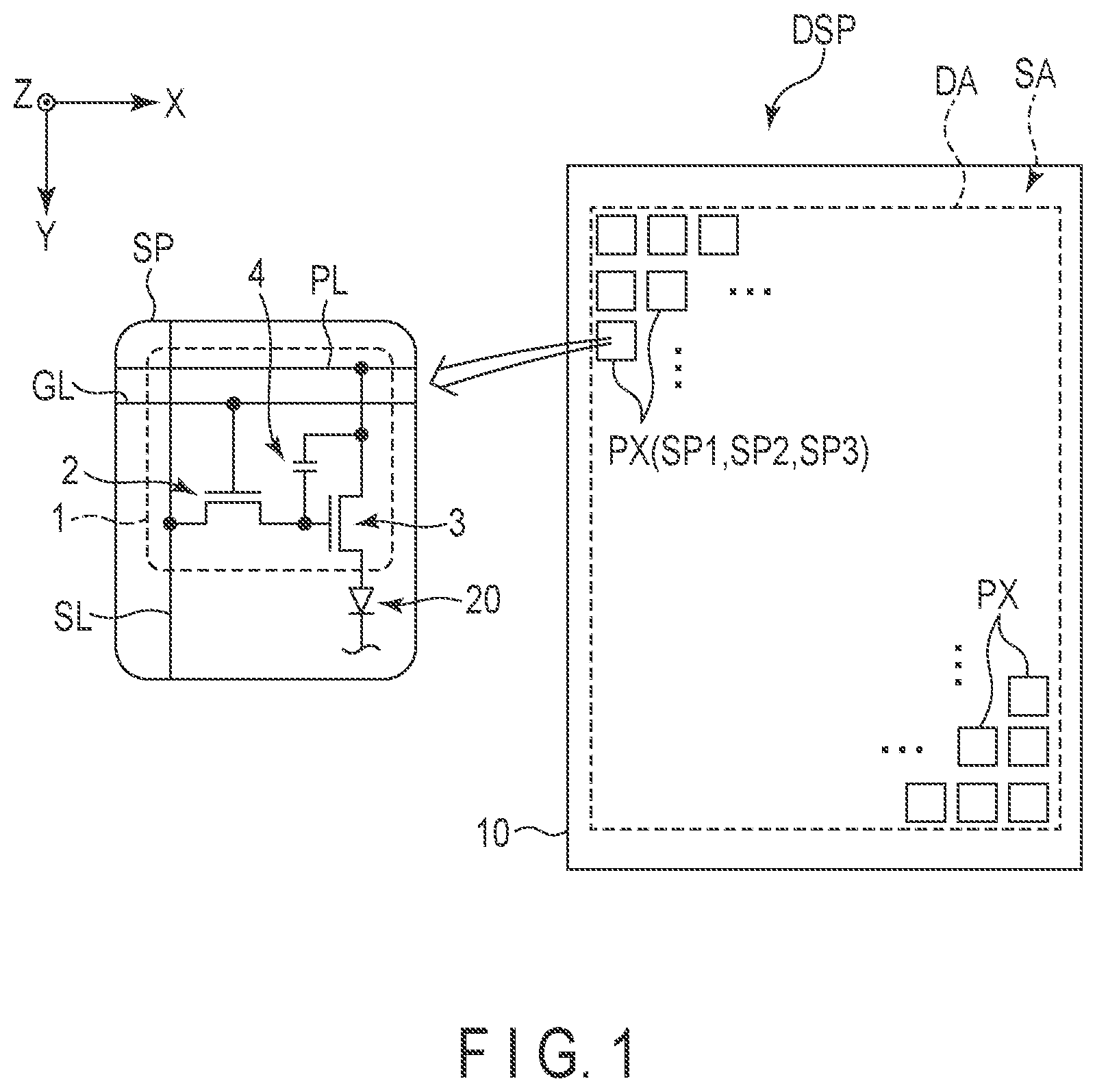
The embodiments described herein aim to provide a display device manufacturing method capable of suppressing the reduction in reliability. In general, according to one embodiment, a display device manufacturing method comprises: preparing a processing substrate on which a first lower electrode of a first sub-pixel, a second lower electrode of a second sub-pixel, and a third lower electrode of a third sub-pixel are formed, and a rib including a first aperture overlapping the first lower electrode, a second aperture overlapping the second lower electrode, and a third aperture overlapping the third lower electrode is formed; forming a first thin film including a first light emitting layer over the first sub-pixel, the second sub-pixel, and the third sub-pixel; forming a negative first resist exposing the first thin film of the second sub-pixel and the third sub-pixel and covering the first thin film of the first sub-pixel; removing the first thin film of the second sub-pixel and the third sub-pixel using the first resist as a mask, leaving the first thin film in the first sub-pixel, exposing the second lower electrode from the second aperture, and exposing the third lower electrode from the third aperture; removing the first resist; forming a second thin film including a second light emitting layer over the first sub-pixel, the second sub-pixel, and the third sub-pixel; forming a negative second resist exposing the second thin film of the third sub-pixel and covering the second thin film of the first sub-pixel and the second sub-pixel; removing the second thin film of the third sub-pixel using the second resist as a mask, leaving the second thin film in the first sub-pixel and the second sub-pixel, and exposing the third lower electrode from the third aperture; removing the second resist; forming a positive third resist exposing the second thin film of the first sub-pixel, and covering the second thin film of the second sub-pixel and the third lower electrode of the third sub-pixel; removing the second thin film of the first sub-pixel using the third resist as a mask; and removing the third resist. According to one embodiment, a display device manufacturing method capable of suppressing the reduction in reliability can be provided. An embodiment will be described hereinafter with reference to the accompanying drawings. The disclosure is merely an example, and proper changes in keeping with the spirit of the invention, which are easily conceivable by a person of ordinary skill in the art, come within the scope of the invention as a matter of course. In addition, in some cases, in order to make the description clearer, the widths, thicknesses, shapes, etc., of the respective parts are schematically illustrated in the drawings, compared to the actual modes. However, the schematic illustration is merely an example, and adds no restrictions to the interpretation of the invention. In addition, in the specification and drawings, structural elements which function in the same or a similar manner to those described in connection with preceding drawings are denoted by like reference numbers, detailed description thereof being omitted unless necessary. In the figures, an X-axis, a Y-axis and a Z-axis orthogonal to each other are described to facilitate understanding as needed. A direction along the X-axis is referred to as a first direction, a direction along the Y-axis is referred to as a second direction, and a direction along the Z-axis is referred to as a third direction. Viewing various elements parallel to the third direction Z is referred to as plan view. The display device of this embodiment is an organic electroluminescent display device comprising an organic light emitting diode (OLED) as a display element, and can be mounted on televisions, personal computers, vehicle-mounted devices, tablet terminals, smartphones, mobile phones, and the like. is a view showing a configuration example of a display device DSP. The display device DSP has a display area DA where images are displayed and a surrounding area SA around the display area DA, on an insulating substrate 10 . The substrate 10 may be glass or a flexible resin film. In the embodiment, the shape of the substrate 10 in plan view is a rectangular shape. However, the shape of the substrate 10 in plan view is not limited to a rectangular shape, but may be any other shape such as a square, a circle or an ellipse. The display area DA includes a plurality of pixels PX arrayed in a matrix in the first direction X and the second direction Y. Each of the pixels PX includes a plurality of sub-pixels SP. As an example, the pixel PX includes a sub-pixel SP 1 of a first color, a sub-pixel SP 2 of a second color, and a sub-pixel SP 3 of a third color. The first, second, and third colors are colors different from each other. Incidentally, the pixel PX may include sub-pixels SP of other colors such as a white color together with the sub-pixels SP 1 , SP 2 , and SP 3 or instead of any of the sub-pixels SP 1 , SP 2 , and SP 3 . The sub-pixel SP comprises a pixel circuit 1 and a display element 20 driven by the pixel circuit 1 . The pixel circuit 1 comprises a pixel switch 2 , a drive transistor 3 , and a capacitor 4 . The pixel switch 2 and the drive transistor 3 are, for example, switching elements constituted by thin-film transistors. A gate electrode of the pixel switch 2 is connected to a scanning line GL. One of a source electrode and a drain electrode of the pixel switch 2 is connected to a signal line SL, and the other is connected to a gate electrode of the drive transistor 3 and the capacitor 4 . In the drive transistor 3 , one of the source electrode and the drain electrode is connected to the power line PL and the capacitor 4 , and the other is connected to an anode of a display element 20 . Incidentally, the configuration of the pixel circuit 1 is not limited to the example shown in the figure. For example, the pixel circuit 1 may comprise more thin-film transistors and capacitors. The display element 20 is an organic light-emitting diode (OLED) as a light-emitting element and may be referred to as an organic EL element. is a view showing an example of a layout of the sub-pixels SP 1 , SP 2 , and SP 3 . In the example of , the sub-pixels SP 2 and SP 3 are arranged in the second direction Y. Furthermore, each of the sub-pixels SP 2 and SP 3 is arranged with the sub-pixels SP 1 in the first direction X. When the sub-pixels SP 1 , SP 2 , and SP 3 are arranged in such a layout, a column in which the sub-pixels SP 2 and SP 3 are alternately arranged in the second direction Y and a column in which a plurality of sub-pixels SP 1 are arranged in the second direction Y are formed in the display area DA. These columns are alternately arranged in the first direction X. Incidentally, the layout of the sub-pixels SP 1 , SP 2 , and SP 3 is not limited to the example in . As another example, the sub-pixels SP 1 , SP 2 , and SP 3 in each pixel PX may be arranged in order in the first direction X. A rib 5 and a partition 6 are arranged in the display area DA. The rib 5 includes apertures AP 1 , AP 2 , and AP 3 in the sub-pixels SP 1 , SP 2 , and SP 3 , respectively. The partition 6 overlaps the rib 5 in plan view. The partition 6 includes a plurality of first partitions 6 x extending in the first direction X and a plurality of second partitions 6 y extending in the second direction Y. The plurality of first partitions 6 x are located between the apertures AP 2 and AP 3 adjacent in the second direction Y and between two apertures AP 1 adjacent in the second direction Y. The second partitions 6 y are located between the apertures AP 1 and AP 2 adjacent in the first direction X and between the apertures AP 1 and AP 3 adjacent in the first direction X. In the example in , the first partitions 6 x and the second partitions 6 y are connected to each other. As a result, the partition 6 is formed to have a grating pattern surrounding the apertures AP 1 , AP 2 , and AP 3 as a whole. The partition 6 is considered to include apertures at the sub-pixels SP 1 , SP 2 , and SP 3 , similarly to the rib 5 . The sub-pixels SP 1 , SP 2 , and SP 3 comprise display elements 201 , 202 , and 203 as display elements 20 , respectively. The sub-pixel SP 1 comprises a lower electrode LE 1 , an upper electrode UE 1 , and an organic layer OR 1 each overlapping the aperture AP 1 . The sub-pixel SP 2 comprises a lower electrode LE 2 , an upper electrode UE 2 , and an organic layer OR 2 each overlapping the aperture AP 2 . The sub-pixel SP 3 comprises a lower electrode LE 3 , an upper electrode UE 3 , and an organic layer OR 3 each overlapping the aperture AP 3 . In the example in , outlines of the lower electrodes LE 1 , LE 2 , and LE 3 are represented by dotted lines, and outlines of the organic layers OR 1 , OR 2 , and OR 3 and the upper electrodes UE 1 , UE 2 , and UE 3 are represented as one-dot chain lines. A peripheral portion of each of the lower electrodes LE 1 , LE 2 , and LE 3 overlaps the rib 5 . The outlines of the respective lower electrode, organic layer, and upper electrode shown in the figure may not reflect the exact shapes. The lower electrode LE 1 , the upper electrode UE 1 , and the organic layer OR 1 constitute the display element 201 of the sub-pixel SP 1 . The lower electrode LE 2 , the upper electrode UE 2 , and the organic layer OR 2 constitute the display element 202 of the sub-pixel SP 2 . The lower electrode LE 3 , the upper electrode UE 3 , and the organic layer OR 3 constitute the display element 203 of the sub-pixel SP 3 . For example, the lower electrodes LE 1 , LE 2 , and LE 3 correspond to the anodes of the display elements. The upper electrodes UE 1 , UE 2 , and UE 3 correspond to the cathodes of the display elements or common electrodes. The lower electrode LE 1 is connected to the pixel circuit 1 of the sub-pixel SP 1 (see ) through a contact hole CH 1 . The lower electrode LE 2 is connected to the pixel circuit 1 of the sub-pixel SP 2 through a contact hole CH 2 . The lower electrode LE 3 is connected to the pixel circuit 1 of the sub-pixel SP 3 through a contact hole CH 3 . In the example shown in , the area of the aperture AP 1 is larger than that of the aperture AP 2 , and the area of the aperture AP 2 is larger than that of the aperture AP 3 . In other words, the area of the lower electrode LE 1 exposed through the aperture AP 1 is larger than the area of the lower electrode LE 2 exposed through the aperture AP 2 , and the area of the lower electrode LE 2 exposed through the aperture AP 2 is larger than the area of the lower electrode LE 3 exposed through the aperture AP 3 . For example, the display element 201 of the sub-pixel SP 1 is configured to emit light in the blue wavelength range. In addition, the display element 202 of the sub-pixel SP 2 is configured to emit light in the green wavelength range, and the display element 203 of the sub-pixel SP 3 is configured to emit light in the red wavelength range. is a schematic cross-sectional view showing the display device DSP taken along line III-III in . A circuit layer 11 is arranged on the above-described substrate 10 . The circuit layer 11 includes various circuits such as the pixel circuits 1 , and various lines such as the scanning lines GL, the signal lines SL and the power lines PL shown in . The circuit layer 11 is covered with an insulating layer 12 . The insulating layer 12 functions as a planarization film for planarizing uneven parts generated by the circuit layer 11 . The lower electrodes LE 1 , LE 2 , and LE 3 are arranged on the insulating layer 12 . The rib 5 is arranged on the insulating layer 12 and the lower electrodes LE 1 , LE 2 , and LE 3 . End parts of the lower electrodes LE 1 , LE 2 , and LE 3 are covered with the rib 5 . In other words, the end parts of the lower electrodes LE 1 , LE 2 , LE 3 are located between the insulating layer 12 and the rib 5 . The insulating layer 12 is covered with the rib 5 at a position between adjacent lower electrodes of the lower electrodes LE 1 , LE 2 , and LE 3 . The partition 6 includes a lower portion (stem) 61 arranged on the rib 5 and an upper portion (shade) 62 arranged on the lower portion 61 . The lower portion 61 of the partition 6 shown on the right side of the figure is located between the apertures AP 1 and AP 2 . The lower portion 61 of the partition 6 shown on the left side of the figure is located between the apertures AP 2 and AP 3 . The upper portion 62 has a width greater than the lower portion 61 . As a result, both the end parts of the upper portion 62 protrude from the side surfaces of the lower portion 61 in . The shape of the partition 6 may also be referred to as an overhanging shape. A part of the upper portion 62 , which further protrudes toward the aperture AP 1 than the lower portion 61 is referred to as a protrusion 621 , a part which further protrudes toward the aperture AP 2 than the lower portion 61 is referred to as a protrusion 622 , and a part which further protrudes toward the aperture AP 3 than the lower portion 61 is referred to as a protrusion 623 . The organic layer OR 1 is in contact with the lower electrode LE 1 through the aperture AP 1 , covers the lower electrode LE 1 , and partially overlaps the rib 5 . The upper electrode UE 1 is opposed to the lower electrode LE 1 and arranged on the organic layer OR 1 . Furthermore, the upper electrode UE 1 is in contact with side surfaces of the lower portion 61 . The organic layer OR 1 and the upper electrode UE 1 are located below the upper portion 62 . The organic layer OR 2 is in contact with the lower electrode LE 2 through the aperture AP 2 , covers the lower electrode LE 2 , and partially overlaps the rib 5 . The upper electrode UE 2 is opposed to the lower electrode LE 2 and arranged on the organic layer OR 2 . Furthermore, the upper electrode UE 2 is in contact with the side surfaces of the lower portion 61 . The organic layer OR 2 and the upper electrode UE 2 are located below the upper portion 62 . The organic layer OR 3 is in contact with the lower electrode LE 3 through the aperture AP 3 , covers the lower electrode LE 3 , and partially overlaps the rib 5 . The upper electrode UE 3 is opposed to the lower electrode LE 3 and arranged on the organic layer OR 3 . Furthermore, the upper electrode UE 3 is in contact with the side surfaces of the lower portion 61 . The organic layer OR 3 and the upper electrode UE 3 are located below the upper portion 62 . In the example of , the sub-pixels SP 1 , SP 2 , and SP 3 include cap layers (optical adjustment layers) CP 1 , CP 2 , and CP 3 for adjusting the optical characteristics of the light emitted from the light emitting layers of the organic layers OR 1 , OR 2 , and OR 3 . The cap layer CP 1 is located in the aperture AP 1 , located below the upper portion 62 , and arranged on the upper electrode UE 1 . The cap layer CP 2 is located in the aperture AP 2 , located below the upper portion 62 , and arranged on the upper electrode UE 2 . The cap layer CP 3 is located in the aperture AP 3 , located below the upper portion 62 , and arranged on the upper electrode UE 3 . Sealing layers SE 1 , SE 2 , and SE 3 are arranged in the sub-pixels SP 1 , SP 2 , and SP 3 , respectively. The sealing layer SE 1 is in contact with the cap layer CP 1 , and the lower portion 61 and the upper portion 62 of the partition 6 , and continuously covers members of the sub-pixel SP 1 . The sealing layer SE 2 is in contact with the cap layer CP 2 , and the lower portion 61 and the upper portion 62 of the partition 6 , and continuously covers members of the sub-pixel SP 2 . The sealing layer SE 3 is in contact with the cap layer CP 3 , and the lower portion 61 and the upper portion 62 of the partition 6 , and continuously covers members of the sub-pixel SP 3 . The sealing layers SE 1 , SE 2 , and SE 3 are covered with a protective layer 13 . In the example in , none of the organic layers, the upper electrodes, the cap layers, and the sealing layers are arranged on the partition 6 , but some of these layers may be arranged. For example, when a part of the organic layer is arranged on the partition 6 , a part below the upper portion 62 and a part arranged on the upper portion 62 , of the organic layer, are separated from each other. When a part of the upper electrode is arranged on the partition 6 , a part below the upper portion 62 and a part arranged on the upper portion 62 , of the upper electrode, are separated from each other. When a part of the cap layer is arranged on the partition 6 , a part below the upper portion 62 and a part arranged on the upper portion 62 , of the cap layer, are separated from each other. On the partition 6 between the sub-pixels SP 1 and SP 2 , the organic layer OR 1 is separated from the organic layer OR 2 , the upper electrode UE 1 is separated from the upper electrode UE 2 , the cap layer CP 1 is separated from the cap layer CP 2 , and the sealing layer SE 1 is separated from the sealing layer SE 2 . On the partition 6 between the sub-pixels SP 2 and SP 3 , the organic layer OR 2 is separated from the organic layer OR 3 , the upper electrode UE 2 is separated from the upper electrode UE 3 , the cap layer CP 2 is separated from the cap layer CP 3 , and the sealing layer SE 2 is separated from the sealing layer SE 3 . The insulating layer 12 is an organic insulating layer. The rib 5 and the sealing layers SE 1 , SE 2 , and SE 3 are inorganic insulating layers. The sealing layers SE 1 , SE 2 , and SE 3 are formed of, for example, the same inorganic insulating material. The rib 5 is formed of silicon nitride (SiNx), which is an example of an inorganic insulating material. Incidentally, the rib 5 may be formed as a single-layer body of any one of silicon oxide (SiOx), silicon oxynitride (SiON) and aluminum oxide (Al 2 O 3 ) as the other inorganic insulating material. Alternatively, the rib 5 may be formed as a stacked layer body formed of combination of at least two of a silicon nitride layer, a silicon oxide layer, a silicon oxynitride layer, and an aluminum oxide layer. The sealing layers SE 1 , SE 2 , and SE 3 are formed of silicon nitride (SiNx), which is an example of an inorganic insulating material. The sealing layers SE 1 , SE 2 , and SE 3 may be formed as single-layer bodies of any one of silicon oxide (SiOx), silicon oxynitride (SiON) and aluminum oxide (Al 2 O 3 ) as the other inorganic insulating material. Alternatively, the sealing layers SE 1 , SE 2 , and SE 3 may be formed as stacked layer bodies formed of combination of at least two of a silicon nitride layer, a silicon oxide layer, a silicon oxynitride layer, and an aluminum oxide layer. For this reason, the sealing layers SE 1 , SE 2 , and SE 3 may be formed of the same material as that of the rib 5 . The lower portion 61 of the partition 6 is formed of a conductive material and is electrically connected to each of the upper electrodes UE 1 , UE 2 , and UE 3 . Both the lower portion 61 and the upper portion 62 of the partition 6 may be conductive. The upper portion 62 is formed of a light-shielding material. The thickness of the rib 5 is sufficiently small as compared to the thickness of the partition 6 and the insulating layer 12 . In one example, the thickness of the rib 5 is 200 nm or more and 400 nm or less. The thickness of the lower portion 61 of the partition 6 (thickness from the upper surface of the rib 5 to the lower surface of the upper portion 62 ) is greater than the thickness of the rib 5 . The thickness of the sealing layer SE 1 , the thickness of the sealing layer SE 2 , and the thickness of the sealing layer SE 3 are substantially equal to each other. The silicon nitride has a property of slightly absorbing the blue wavelength (in the wavelength range of 450 nm or less). Therefore, when the sealing layers SE 1 , SE 2 , and SE 3 are formed of silicon nitride, the thickness of the sealing layers SE 1 , SE 2 , and SE 3 is desirably small enough to ensure the sealing performance, for example, 2 μm or less. The transmittance of the blue wavelength is thereby improved. In contrast, when the thickness of the sealing layers SE 1 , SE 2 , and SE 3 is made small, voids may be formed below the protrusions 621 , 622 , and 623 . The lower electrodes LE 1 , LE 2 , and LE 3 may be formed of a transparent conductive material such as ITO and may have a multilayer structure of a metallic material such as silver (Ag) and a transparent conductive material. The upper electrodes UE 1 , UE 2 , and UE 3 are formed of, for example, a metallic material such as an alloy (MgAg) of magnesium and silver. The upper electrodes UE 1 , UE 2 , and UE 3 may be formed of a transparent conductive material such as ITO. Each of the organic layers OR 1 , OR 2 , and OR 3 includes a plurality of functional layers such as a hole-injection layer, a hole-transport layer, an electron blocking layer, a hole blocking layer, an electron-transport layer, and an electron-injection layer. In addition, the organic layer OR 1 includes a light emitting layer EM 1 . The organic layer OR 2 includes a light emitting layer EM 2 . The light emitting layer EM 2 is formed of a material different from the light emitting layer EM 1 . The organic layer OR 3 includes a light emitting layer EM 3 . The light emitting layer EM 3 is formed of a material different from that of the light emitting layers EM 1 and EM 2 . The material forming the light emitting layer EM 1 , the material forming the light emitting layer EM 2 , and the material forming the light emitting layer EM 3 are materials that emit light in wavelength ranges different from each other. In one example, the light emitting layer EM 1 is formed of a material which emits light in the blue wavelength range, the light emitting layer EM 2 is formed of a material which emits light in the green wavelength range, and the light emitting layer EM 3 is formed of a material which emits light in the red wavelength range. The cap layers CP 1 , CP 2 , and CP 3 are formed of, for example, multilayer bodies of transparent thin films. The multilayer body may include a thin film formed of an inorganic material and a thin film formed of an organic material, as the thin films. In addition, the plurality of thin films have refractive indexes different from each other. The materials of the thin films constituting the multilayer bodies are different from the materials of the upper electrodes UE 1 , UE 2 , and UE 3 and also different from the materials of the sealing layers SE 1 , SE 2 , and SE 3 . Incidentally, the cap layers CP 1 , CP 2 , and CP 3 may be omitted. The protective layer 13 is formed of a multilayer body of transparent thin films and includes, for example, a thin film formed of inorganic materials and a thin film formed of organic materials, as the thin films. A common voltage is supplied to the partition 6 . This common voltage is supplied to each of the upper electrodes UE 1 , UE 2 , and UE 3 which are in contact with the side surfaces of the lower portion 61 . A pixel voltage is supplied to the lower electrodes LE 1 , LE 2 , and LE 3 through the pixel circuits 1 included in the respective sub-pixels SP 1 , SP 2 , and SP 3 . When a potential difference is formed between the lower electrode LE 1 and the upper electrode UE 1 , the light emitting layer EM 1 of the organic layer OR 1 emits light in the first wavelength range. When a potential difference is formed between the lower electrode LE 2 and the upper electrode UE 2 , the light emitting layer EM 2 of the organic layer OR 2 emits light in the second wavelength range. When a potential difference is formed between the lower electrode LE 3 and the upper electrode UE 3 , the light emitting layer EM 3 of the organic layer OR 3 emits light in the third wavelength range. Next, an example of a method of manufacturing the display device DSP will be described. is a flowchart illustrating an example of the method of manufacturing the display device DSP. The manufacturing method illustrated here roughly includes a process of preparing a processing substrate SUB including the sub-pixels SP 1 , SP 2 , and SP 3 (step ST 1 ), a process of forming the display element 201 of the sub-pixel SP 1 (step ST 2 ), a process of forming the display element 202 of the sub-pixel SP 2 (step ST 3 ), and a process of forming the display element 203 of the sub-pixel SP 3 (step ST 4 ). In step ST 1 , first, the processing substrate SUB in which the lower electrode LE 1 of the sub-pixel SP 1 , the lower electrode LE 2 of the sub-pixel SP 2 , the lower electrode LE 3 of the sub-pixel SP 3 , the rib 5 , and the partition 6 are formed, on the substrate 10 , is prepared. As shown in , the circuit layer 11 and the insulating layer 12 are also formed between the substrate 10 and the lower electrodes LE 1 , LE 2 , and LE 3 . In step ST 2 , first, the first thin film 31 including the light emitting layer EM 1 is formed over the sub-pixel SP 1 , the sub-pixel SP 2 , and the sub-pixel SP 3 (step ST 21 ). After that, a negative first resist 41 patterned in a predetermined shape is formed on the first thin film 31 (step ST 22 ). The first resist 41 exposes the first thin film 31 of the sub-pixel SP 2 and the sub-pixel SP 3 , and covers the first thin film 31 of the sub-pixel SP 1 . After that, the first thin film 31 of the sub-pixel SP 2 and the sub-pixel SP 3 is removed by etching using the first resist 41 as a mask (step ST 23 ). The first thin film 31 remains in the sub-pixel SP 1 . After that, the first resist 41 is removed (step ST 24 ). The sub-pixel SP 1 is thereby formed. The sub-pixel SP 1 comprises the display element 201 including the first thin film 31 in a predetermined shape. In step ST 3 , first, the second thin film 32 including the light emitting layer EM 2 is formed over the sub-pixel SP 1 , the sub-pixel SP 2 , and the sub-pixel SP 3 (step ST 31 ). After that, a negative second resist 42 patterned in a predetermined shape is formed on the second thin film 32 (step ST 32 ). The second resist 42 exposes the second thin film 32 of the sub-pixel SP 3 and covers the second thin film 32 of the sub-pixel SP 1 and the sub-pixel SP 2 . After that, the second thin film 32 of the sub-pixel SP 3 is removed by etching using the second resist 42 as a mask (step ST 33 ). The second thin film 32 remains in the sub-pixel SP 1 and the sub-pixel SP 2 . After that, the second resist 42 is removed (step ST 34 ). After that, a positive third resist 43 patterned in a predetermined shape is formed (step ST 35 ). The third resist 43 exposes the second thin film 32 of the sub-pixel SP 1 , covers the second thin film 32 of the sub-pixel SP 2 , and covers the lower electrode LE 3 of the sub-pixel SP 3 . After that, the second thin film 32 of the sub-pixel SP 1 is removed by etching using the third resist 43 as a mask (step ST 36 ). The first thin film 31 remains in the sub-pixel SP 1 , and the second thin film 32 remains in the sub-pixel SP 2 . After that, the third resist 43 is removed (step ST 37 ). The sub-pixel SP 2 is thereby formed. The sub-pixel SP 2 comprises the display element 202 including the second thin film 32 in a predetermined shape. In step ST 4 , first, the third thin film 33 including the light emitting layer EM 3 is formed over the sub-pixel SP 1 , the sub-pixel SP 2 , and the sub-pixel SP 3 (step ST 41 ). After that, a positive fourth resist 44 patterned in a predetermined shape is formed on the third thin film 33 (step ST 42 ). The fourth resist 44 exposes the third thin films 33 of the sub-pixel SP 1 and the sub-pixel SP 2 , and covers the third thin film 33 of the sub-pixel SP 3 . After that, the third thin film 33 of the sub-pixel SP 1 and the sub-pixel SP 2 is removed by etching using the fourth resist 44 as a mask (step ST 43 ). The third thin film 33 remains in the sub-pixel SP 3 . After that, the fourth resist 44 is removed (step ST 44 ). The sub-pixel SP 3 is thereby formed. The sub-pixel SP 3 comprises the display element 203 including the third thin film 33 in a predetermined shape. A negative type resist is a material which is insoluble in a developing solution when exposed, while a positive type resist is a material which dissolves in the developing solution when exposed. Step ST 1 to step ST 4 will be described below with reference to to . First, in step ST 1 , the processing substrate SUB is prepared as shown in . A process of preparing the processing substrate SUB includes a process of forming the circuit layer 11 on the substrate 10 , a process of forming the insulating layer 12 on the circuit layer 11 , a process of forming the lower electrode LE 1 of the sub-pixel SP 1 , the lower electrode LE 2 of the sub-pixel SP 2 , and the lower electrode LE 3 of the sub-pixel SP 3 on the insulating layer 12 , a process of forming the rib 5 including the apertures AP 1 , AP 2 , and AP 3 which overlap the lower electrodes LE 1 , LE 2 , and LE 3 , respectively, and a process of forming the partition 6 including the lower portion 61 arranged on the rib 5 and the upper portion 62 arranged on the lower portion 61 and protruding from the side surfaces of the lower portion 61 . In to , illustration of the substrate 10 and the circuit layer 11 lower than the insulating layer 12 is omitted. Then, in step ST 21 , as shown in , the first thin film 31 is formed over the sub-pixel SP 1 , the sub-pixel SP 2 , and the sub-pixel SP 3 . The first thin film 31 overlaps the lower electrode LE 1 in the aperture AP 1 of the sub-pixel SP 1 , overlaps the lower electrode LE 2 in the aperture AP 2 of the sub-pixel SP 2 , overlaps the lower electrode LE 3 in the aperture AP 3 of the sub-pixel SP 3 , overlaps the rib 5 , and covers the lower portion 61 and the upper portion 62 of the partition 6 . is an enlarged cross-sectional view showing the first thin film 31 arranged in the sub-pixel SP 1 . The first thin film 31 includes an organic layer OR 1 including a light emitting layer EM 1 which emits light in the blue wavelength range, an upper electrode UE 1 arranged on the organic layer OR 1 , a cap layer CP 1 arranged on the upper electrode UE 1 , and a sealing layer SE 1 arranged on the cap layer CP 1 . The first thin film 31 arranged on the sub-pixel SP 2 and the sub-pixel SP 3 is also formed in the same manner as the first thin film shown in . Then, in step ST 22 , the first resist 41 is formed on the first thin film 31 as shown in . First, the first resist 41 is applied over the entire surface on the first thin film 31 as shown in an upper part of . At this time, the first resist 41 is embedded in the voids of the first thin film 31 formed below the protrusions 621 , 622 , and 623 . After that, as shown in the middle part of , the first resist 41 is exposed by applying a photomask M 1 having a predetermined aperture pattern. As described above, the first resist 41 is a negative resist. A photomask M 1 having an aperture pattern corresponding to the sub-pixel SP 1 is applied. As a result, the first resist 41 of the sub-pixel SP 1 is exposed, while the first resist 41 of the sub-pixel SP 2 and the sub-pixel SP 3 is not exposed. After that, as shown in the lower part of , the first resist 41 is cured after the first resist 41 is developed. As a result, the first resist 41 covers the first thin film 31 of the sub-pixel SP 1 and exposes the first thin film 31 of the sub-pixel SP 2 and the sub-pixel SP 3 . In addition, the first resist 41 remains in the void below the protrusion 621 and is removed from the voids below the protrusions 622 and 623 . Then, in step ST 23 , as shown in the upper part of , etching is performed using the first resist 41 as a mask to remove the first thin film 31 of the sub-pixel SP 2 and the sub-pixel SP 3 exposed from the first resist 41 , and the first thin film 31 remains in the sub-pixel SP 1 . In other words, the sealing layer SE 1 , the cap layer CP 1 , the upper electrode UE 1 , and the organic layer OR 1 in the sub-pixel SP 2 and the sub-pixel SP 3 are removed. As a result, the lower electrode LE 2 is exposed through the aperture AP 2 in the sub-pixel SP 2 , and the rib 5 surrounding the lower electrode LE 2 is also exposed. In addition the lower electrode LE 3 is exposed through the aperture AP 3 in the sub-pixel SP 3 , and the rib 5 surrounding the lower electrode LE 3 is also exposed. Then, in step ST 24 , the first resist 41 is removed as shown in the middle part of . The first thin film 31 of the sub-pixel SP 1 is thereby exposed. The display element 201 is formed in the sub-pixel SP 1 through steps ST 21 to ST 24 . Then, in step ST 31 , as shown in a lower part of , the second thin film 32 is formed over the sub-pixel SP 1 , sub-pixel SP 2 , and the sub-pixel SP 3 . The second thin film 32 overlaps the first thin film 31 of the sub-pixel SP 1 , overlaps the lower electrode LE 2 in the aperture AP 2 of the sub-pixel SP 2 , overlaps the lower electrode LE 3 in the aperture AP 3 of the sub-pixel SP 3 , overlaps the rib 5 , and covers the lower portion 61 and the upper portion 62 of the partition 6 . As shown in , the second thin film 32 includes an organic layer OR 2 including a light emitting layer EM 2 which emits light in the green wavelength range, an upper electrode UE 2 arranged on the organic layer OR 2 , a cap layer CP 2 arranged on the upper electrode UE 2 , and a sealing layer SE 2 arranged on the cap layer CP 2 . Then, in step ST 32 , the second resist 42 is formed on the second thin film 32 as shown in . First, the second resist 42 is applied over the entire surface on the second thin film 32 , as shown in the upper part of . At this time, the second resist 42 is embedded in the voids of the second thin film 32 formed below the protrusions 621 , 622 , and 623 . After that, as shown in the middle part of , the second resist 42 is exposed by applying a photomask M 2 having a predetermined aperture pattern. As described above, the second resist 42 is a negative resist. A photomask M 2 having an aperture pattern corresponding to the sub-pixel SP 1 and the sub-pixel SP 2 is applied. As a result, the second resist 42 of the sub-pixel SP 1 and the sub-pixel SP 2 is exposed, while the second resist 42 of the sub-pixel SP 3 is not exposed. After that, as shown in the lower part of , the second resist 42 is cured after the second resist 42 is developed. As a result, the second resist 42 covers the second thin film 32 of the sub-pixel SP 1 and the sub-pixel SP 2 and exposes the second thin film 32 of the sub-pixel SP 3 . In addition, the second resist 42 remains in the voids below the protrusions 621 and 622 and is removed from the void below the protrusion 623 . Then, in step ST 33 , as shown in the upper part of , etching is performed using the second resist 42 as a mask to remove the second thin film 32 of the sub-pixel SP 3 exposed from the second resist 42 , and the second thin film 32 remains in the sub-pixel SP 1 and the sub-pixel SP 2 . In other words, the sealing layer SE 2 , the cap layer CP 2 , the upper electrode UE 2 , and the organic layer OR 2 in the sub-pixel SP 3 are removed. As a result, the lower electrode LE 3 is exposed through the aperture AP 3 in the sub-pixel SP 3 , and the rib 5 surrounding the lower electrode LE 3 is also exposed. Then, in step ST 34 , the second resist 42 is removed as shown in the lower part of . The second thin film 32 of the sub-pixel SP 2 is thereby exposed. The display element 202 is formed in the sub-pixel SP 2 through steps ST 31 to ST 34 . In addition, in the sub-pixel SP 1 , the second thin film 32 overlapping the first thin film 31 is exposed. Then, in step ST 35 , the third resist 43 is formed as shown in . First, as shown in an upper part of , the third resist 43 is applied over the sub-pixels SP 1 , SP 2 , and SP 3 . At this time, the third resist 43 overlaps the second thin film 32 of the sub-pixel SP 1 and sub-pixel SP 2 , overlaps the lower electrode LE 3 of the sub-pixel SP 3 and the rib 5 , and covers the partition 6 . In addition, the third resist 43 is embedded in the voids formed below the protrusions 621 , 622 , and 623 . After that, as shown in the middle part of , the third resist 43 is exposed by applying a photomask M 3 having a predetermined aperture pattern. As described above, the third resist 43 is a positive resist. A photomask M 3 having an aperture pattern corresponding to the sub-pixel SP 1 is applied. As a result, the third resist 43 of the sub-pixel SP 1 is exposed, but the third resist 43 below the protrusion 621 is not exposed since the protrusion 621 is formed of a light-shielding material. The third resist 43 of the sub-pixel SP 2 and the sub-pixel SP 3 is not exposed. After that, as shown in the lower part of , the third resist 43 is cured after the third resist 43 is developed. As a result, the third resist 43 covers the second thin film 32 of the sub-pixel SP 2 , covers the lower electrode LE 3 of the sub-pixel SP 3 , and exposes the second thin film 32 of the sub-pixel SP 1 . In addition, the third resist 43 remains in the void below the protrusion 621 . Then, in step ST 36 , as shown in the upper part of , etching is performed using the third resist 43 as a mask to remove the second thin film 32 of the sub-pixel SP 1 exposed from the third resist 43 . At this time, the third resist 43 which remains below the protrusion 621 serves as a mask, and the second thin film 32 partially remains. Then, in step ST 37 , the third resist 43 is removed as shown in the middle part of . Then, in step ST 41 , as shown in a lower part of , the third thin film 33 is formed over the sub-pixel SP 1 , the sub-pixel SP 2 , and the sub-pixel SP 3 . The third thin film 33 overlaps the first thin film 31 of the sub-pixel SP 1 , overlaps the second thin film 32 of the sub-pixel SP 2 , overlaps the lower electrode LE 3 in the aperture AP 3 of the sub-pixel SP 3 , overlaps the rib 5 , and covers the lower portion 61 and the upper portion 62 of the partition 6 . As shown in , the third thin film 33 includes an organic layer OR 3 including a light emitting layer EM 3 which emits light in the red wavelength range, an upper electrode UE 3 arranged on the organic layer OR 3 , a cap layer CP 3 arranged on the upper electrode UE 3 , and a sealing layer SE 3 arranged on the cap layer CP 3 . Then, in step ST 42 , the fourth resist 44 is formed on the third thin film 33 as shown in . First, the fourth resist 44 is applied over the entire surface on the third thin film 33 , as shown in the upper part of . At this time, the fourth resist 44 is embedded in the voids formed below the protrusions 621 , 622 , and 623 . After that, as shown in a middle part of , the fourth resist 44 is exposed by applying a photomask M 4 having a predetermined aperture pattern. As described above, the fourth resist 44 is a positive resist. The photomask M 4 having an aperture pattern corresponding to the sub-pixel SP 1 and the sub-pixel SP 2 is applied. As a result, the fourth resist 44 of the sub-pixel SP 1 and the sub-pixel SP 2 is exposed, while the fourth resist 44 of the sub-pixel SP 3 is not exposed. In addition, the fourth resist 44 below the protrusions 621 and 622 is not exposed since the protrusions 621 and 622 are formed of a light-shielding material. After that, as shown in a lower part of , the fourth resist 44 is cured after the fourth resist 44 is developed. As a result, the fourth resist 44 covers the third thin film 33 of the sub-pixel SP 3 and exposes the third thin film 33 of the sub-pixel SP 1 and the sub-pixel SP 2 . In addition, the fourth resist 44 remains in the voids below the protrusions 621 and 622 . Then, in step ST 43 , as shown in an upper part of , etching is performed using the fourth resist 44 as a mask to remove the third thin film 33 of the sub-pixel SP 1 and the sub-pixel SP 2 exposed from the fourth resist 44 , and the third thin film 33 remains in the sub-pixel SP 3 . In other words, the sealing layer SE 3 , the cap layer CP 3 , the upper electrode UE 3 , and the organic layer OR 3 in the sub-pixel SP 1 and the sub-pixel SP 2 are removed. At this time, the fourth resist 44 which remains below the protrusion 621 and the protrusion 622 serves as a mask, and the third thin film 33 partially remains. Then, in step ST 44 , the fourth resist 44 is removed as shown in the lower part of . The third thin film 33 of the sub-pixel SP 3 is thereby exposed. The display element 203 is formed in the sub-pixel SP 3 through steps ST 41 to ST 44 . The display element 201 is formed in the sub-pixel SP 1 , the display element 202 is formed in the sub-pixel SP 2 , and the display element 203 is formed in the sub-pixel SP 3 , by the above processes. Of the above processes, the light emitting layer EM 1 may be formed of a material which emits light in the red wavelength range in the process of forming the first thin film 31 in step ST 21 , the light emitting layer EM 2 may be formed of a material which emits light in the green wavelength range in the process of forming the second thin film 32 in step ST 31 , and the light emitting layer EM 3 may be formed of a material which emits light in the blue wavelength range in the process of forming the third thin film 33 in step ST 41 . In the above example, the sub-pixel SP 1 corresponds to the first sub-pixel, the aperture AP 1 corresponds to the first aperture, the lower electrode LE 1 corresponds to the first lower electrode, the organic layer OR 1 corresponds to the first organic layer, the light emitting layer EM 1 corresponds to the first light emitting layer, the upper electrode UE 1 corresponds to the first upper electrode, the cap layer CP 1 corresponds to the first cap layer, and the sealing layer SE 1 corresponds to the first sealing layer. In addition, the sub-pixel SP 2 corresponds to the second sub-pixel, the aperture AP 2 corresponds to the second aperture, the lower electrode LE 2 corresponds to the second lower electrode, the organic layer OR 2 corresponds to the second organic layer, the light emitting layer EM 2 corresponds to the second light emitting layer, the upper electrode UE 2 corresponds to the second upper electrode, the cap layer CP 2 corresponds to the second cap layer, and the sealing layer SE 2 corresponds to the second sealing layer. In addition, the sub-pixel SP 3 corresponds to the third sub-pixel, the aperture AP 3 corresponds to the third aperture, the lower electrode LE 3 corresponds to the third lower electrode, the organic layer OR 3 corresponds to the third organic layer, the light emitting layer EM 3 corresponds to the third light emitting layer, the upper electrode UE 3 corresponds to the third upper electrode, the cap layer CP 3 corresponds to the third cap layer, and the sealing layer SE 3 corresponds to the third sealing layer. According to the embodiment, the first resist 41 for patterning the first thin film 31 is a negative resist. When voids of the first thin film 31 are formed below the protrusions 622 and 623 , the first resist 41 embedded below the protrusions 622 and 623 is unexposed and is therefore removed to expose the first thin film 31 (lower part in ). For this reason, when the first thin film 31 is etched, the first thin film 31 below the protrusions 622 and 623 is removed and the partition 6 is exposed (upper part in ). As a result, electric connection between the second thin film 32 , which is to be subsequently formed, and the partition 6 can be made (lower part in ). The second resist 42 for patterning the second thin film 32 is a negative resist. When the void of the second thin film 32 is formed below the protrusion 623 , the second resist 42 embedded below the protrusion 623 is unexposed and is therefore removed to expose the second thin film 32 (lower part in ). For this reason, when the second thin film 32 is etched, the second thin film 32 below the protrusion 623 is removed and the partition 6 is exposed (upper part in ). As a result, electric connection between the third thin film 33 , which is to be subsequently formed, and the partition 6 can be made (lower part in ). In the process of removing the second thin film 32 which overlaps the first thin film 31 of the sub-pixel SP 1 , the third resist 43 for patterning the second thin film 32 is the positive resist. When the void of the second thin film 32 is formed below the protrusion 621 , the third resist 43 embedded below the protrusion 621 is unexposed and therefore remains (lower part in ). For this reason, when the second thin film 32 is etched, the third resist 43 functions as an etching stopper, and the first thin film 31 below the protrusion 621 is protected (upper part in ). As a result, the destruction of the sealing layer SE 1 included in the first thin film 31 is suppressed, and the display failure caused by entry of moisture can be suppressed. In the process of removing the third thin film 33 which overlaps the first thin film 31 of the sub-pixel SP 1 and the third thin film 33 which overlaps the second thin film 32 of the sub-pixel SP 2 , the fourth resist 44 for patterning the third thin film 33 is the positive resist. When the voids of the third thin film 33 are formed below the protrusions 621 and 622 , the fourth resist 44 embedded below the protrusions 621 and 622 is unexposed and therefore remains (lower part in ). For this reason, when the third thin film 33 is etched, the fourth resist 44 functions as an etching stopper, and the first thin film 31 under the protrusion 621 and the second thin film 32 below the protrusion 622 are protected (upper part in ). As a result, the destruction of the sealing layer SE 1 included in the first thin film 31 and the sealing layer SE 2 included in the second thin film 32 is suppressed, and the display failure caused by entry of moisture can be suppressed. As described above, according to the embodiment, the display device manufacturing method capable of suppressing the reduction in reliability and improving the manufacturing yield can be provided. All of the methods of manufacturing display devices that can be implemented by a person of ordinary skill in the art through arbitrary design changes to the methods of manufacturing display devices described above as embodiments of the present invention come within the scope of the present invention as long as they are in keeping with the spirit of the present invention. Various types of the modified examples are easily conceivable within the category of the ideas of the present invention by a person of ordinary skill in the art and the modified examples are also considered to fall within the scope of the present invention. For example, additions, deletions or changes in design of the constituent elements or additions, omissions, or changes in condition of the processes arbitrarily conducted by a person of ordinary skill in the art, in the above embodiments, fall within the scope of the present invention as long as they are in keeping with the spirit of the present invention. In addition, the other advantages of the aspects described in the embodiments, which are obvious from the descriptions of the present specification or which can be arbitrarily conceived by a person of ordinary skill in the art, are considered to be achievable by the present invention as a matter of course.
Figures (15)
Citations
This patent cites (22)
- US2004/0160170
- US2005/0032453
- US2009/0009069
- US2012/0276484
- US2013/0084531
- US2016/0190508
- US2016/0380040
- US2017/0141180
- US2019/0363275
- US2022/0077251
- US2000-36385
- US2000-195677
- US2003-317949
- US2004-207217
- US2008-135325
- US2009-32673
- US2010-118191
- US2012-238580
- US2013-84576
- US2017-529651
- US2016/019273
- US2018/179308